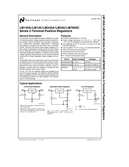
LM140A/LM140/LM340A/LM340/LM7800C Series 3-Terminal ...
LM140A/LM140/LM340A/LM340/LM7800C Series 3-Terminal ...
LM140A/LM140/LM340A/LM340/LM7800C Series 3-Terminal ...

Create successful ePaper yourself
Turn your PDF publications into a flip-book with our unique Google optimized e-Paper software.
<strong><strong>LM140</strong>A</strong><strong>LM140</strong><strong><strong>LM340</strong>A</strong><strong>LM340</strong><strong>LM7800C</strong><br />
<strong>Series</strong> 3-<strong>Terminal</strong> Positive Regulators<br />
General Description<br />
The <strong><strong>LM140</strong>A</strong><strong>LM140</strong><strong><strong>LM340</strong>A</strong><strong>LM340</strong><strong>LM7800C</strong> monolithic<br />
3-terminal positive voltage regulators employ internal current-limiting<br />
thermal shutdown and safe-area compensation<br />
making them essentially indestructible If adequate<br />
heat sinking is provided they can deliver over 10A output<br />
current They are intended as fixed voltage regulators in a<br />
wide range of applications including local (on-card) regulation<br />
for elimination of noise and distribution problems associated<br />
with single-point regulation In addition to use as fixed<br />
voltage regulators these devices can be used with external<br />
components to obtain adjustable output voltages and currents<br />
Considerable effort was expended to make the entire series<br />
of regulators easy to use and minimize the number of external<br />
components It is not necessary to bypass the output<br />
although this does improve transient response Input bypassing<br />
is needed only if the regulator is located far from<br />
the filter capacitor of the power supply<br />
The 5V 12V and 15V regulator options are available in the<br />
steel TO-3 power package The <strong><strong>LM340</strong>A</strong><strong>LM340</strong><strong>LM7800C</strong><br />
series is available in the TO-220 plastic power package and<br />
the LM7805 and LM7812 are also available in the surfacemount<br />
TO-263 package<br />
Typical Applications<br />
Fixed Output Regulator<br />
TLH7781–1<br />
Required if the regulator is located far from the<br />
power supply filter<br />
Although no output capacitor is needed for stability<br />
it does help transient response (If needed<br />
use 01 mF ceramic disc)<br />
Adjustable Output Regulator<br />
January 1995<br />
Features<br />
Y Complete specifications at 1A load<br />
Y Output voltage tolerances of g2% at Tj e 25C and<br />
g4% over the temperature range (<strong><strong>LM140</strong>A</strong><strong><strong>LM340</strong>A</strong>)<br />
Y Line regulation of 001% of VOUTV of DVIN at 1A load<br />
(<strong><strong>LM140</strong>A</strong><strong><strong>LM340</strong>A</strong>)<br />
Y Load regulation of 03% of VOUTA (<strong><strong>LM140</strong>A</strong><strong><strong>LM340</strong>A</strong>)<br />
Y Internal thermal overload protection<br />
Y Internal short-circuit current limit<br />
Y Output transistor safe area protection<br />
Y Pa Product Enhancement tested<br />
Device Output Voltages Packages<br />
<strong><strong>LM140</strong>A</strong><strong>LM140</strong> 5 12 15 TO-3 (K)<br />
<strong><strong>LM340</strong>A</strong><strong>LM340</strong> 5 12 15 TO-3 (K) TO-220 (T)<br />
<strong>LM7800C</strong> 5 6 8 12 15 TO-220 (T) TO-263 (S)<br />
18 24 (5V and 12V only)<br />
TLH7781–2<br />
V OUT e 5V a (5VR1 a I Q) R2 5VR1 l 3I Q<br />
load regulation (L r) (R1 a R2)R1 (L r of<br />
<strong>LM340</strong>-5)<br />
Current Regulator<br />
TLH7781–3<br />
IOUT e V2-3<br />
R1 a IQ DIQ e 13 mA over line and load changes<br />
C1995 National Semiconductor Corporation TLH7781<br />
RRD-B30M115Printed in U S A<br />
<strong><strong>LM140</strong>A</strong><strong>LM140</strong><strong><strong>LM340</strong>A</strong><strong>LM340</strong><strong>LM7800C</strong> <strong>Series</strong> 3-<strong>Terminal</strong> Positive Regulators
Absolute Maximum Ratings (Note 1)<br />
If MilitaryAerospace specified devices are required<br />
please contact the National Semiconductor Sales<br />
OfficeDistributors for availability and specifications<br />
(Note 5)<br />
DC Input Voltage<br />
All Devices except LM7824LM7824C 35V<br />
LM7824LM7824C 40V<br />
Internal Power Dissipation (Note 2) Internally Limited<br />
Maximum Junction Temperature 150C<br />
Storage Temperature Range<br />
Lead Temperature (Soldering 10 sec)<br />
b65Ctoa150C<br />
TO-3 Package (K) 300C<br />
TO-220 Package (T) TO-263 Package (S) 230C<br />
ESD Susceptibility (Note 3) 2 kV<br />
<strong><strong>LM140</strong>A</strong><strong><strong>LM340</strong>A</strong><br />
Operating Conditions (Note 1)<br />
Temperature Range (TA) (Note 2)<br />
<strong><strong>LM140</strong>A</strong> <strong>LM140</strong><br />
<strong><strong>LM340</strong>A</strong> <strong>LM340</strong> LM7805C<br />
b55Ctoa125C<br />
LM7812C LM7815C<br />
LM7806C LM7808C LM7818C<br />
0Ctoa70C<br />
LM7824C 0Ctoa125C<br />
Electrical Characteristics<br />
I OUT e 1A b55C s T J s a150C (<strong><strong>LM140</strong>A</strong>) or 0C s T J s a 125C (<strong><strong>LM340</strong>A</strong>) unless otherwise specified (Note 4)<br />
Output Voltage 5V 12V 15V<br />
Symbol Input Voltage (unless otherwise noted) 10V 19V 23V Units<br />
Parameter Conditions Min Typ Max Min Typ Max Min Typ Max<br />
V O Output Voltage T J e 25C 49 5 51 1175 12 1225 147 15 153 V<br />
P D s 15W 5 mA s I O s 1A 48 52 115 125 144 156 V<br />
V MIN s VIN s VMAX (75 s VIN s 20) (148 s VIN s 27) (179 s VIN s 30) V<br />
DV O Line Regulation I O e 500 mA 10 18 22 mV<br />
DV IN (75 s VIN s 20) (148 s VIN s 27) (179 s VIN s 30) V<br />
TJ e 25C 3 10 4 18 4 22 mV<br />
DVIN (75 s VIN s 20) (145 s VIN s 27) (175 s VIN s 30) V<br />
TJ e 25C<br />
Over Temperature<br />
4<br />
12<br />
9<br />
30<br />
10<br />
30<br />
mV<br />
mV<br />
DVIN (8 s VIN s 12) (16 s VIN s 22) (20 s VIN s 26) V<br />
DV O Load Regulation T J e 25C 5mAsI O s15A 10 25 12 32 12 35 mV<br />
250 mA s I O s 750 mA 15 19 21 mV<br />
Over Temperature<br />
5mAsIO s1A<br />
25 60 75 mV<br />
IQ Quiescent Current TJ e 25C<br />
Over Temperature<br />
6<br />
65<br />
6<br />
65<br />
6<br />
65<br />
mA<br />
mA<br />
DIQ Quiescent Current 5 mA s IO s 1A 05 05 05 mA<br />
Change<br />
TJ e 25C IO e 1A 08 08 08 mA<br />
VMIN s VIN s VMAX (75 s VIN s 20) (148 s VIN s 27) (179 s VIN s 30) V<br />
IO e 500 mA 08 08 08 mA<br />
VMIN s VIN s VMAX (8 s VIN s 25) (15 s VIN s 30) (179 s VIN s 30) V<br />
VN Output Noise Voltage TA e 25C 10 Hz s f s 100 kHz 40 75 90 mV<br />
DVIN<br />
DVOUT<br />
Ripple Rejection TJ e 25C f e 120 Hz IO e 1A<br />
or f e 120 Hz IO e 500 mA<br />
Over Temperature<br />
68<br />
68<br />
80 61<br />
61<br />
72 60<br />
60<br />
70 dB<br />
dB<br />
VMIN s VIN s VMAX (8 s VIN s 18) (15 s VIN s 25) (185 s VIN s 285) V<br />
RO Dropout Voltage<br />
Output Resistance<br />
TJ e 25C IO e 1A<br />
f e 1 kHz<br />
20<br />
8<br />
20<br />
18<br />
20<br />
19<br />
V<br />
mX<br />
Short-Circuit Current<br />
Peak Output Current<br />
Average TC of VO TJ e 25C<br />
TJ e 25C<br />
Min TJ e 0C IO e 5mA<br />
21<br />
24<br />
b06<br />
15<br />
24<br />
b15<br />
12<br />
24<br />
b18<br />
A<br />
A<br />
mVC<br />
VIN Input Voltage TJ e 25C<br />
Required to Maintain<br />
Line Regulation<br />
75 145 175 V<br />
2
<strong>LM140</strong><br />
Electrical Characteristics (Note 4) b55C s TJ<br />
s a150C unless otherwise specified<br />
Output Voltage 5V 12V 15V<br />
Symbol Input Voltage (unless otherwise noted) 10V 19V 23V Units<br />
Parameter Conditions Min Typ Max Min Typ Max Min Typ Max<br />
V O Output Voltage T J e 25C5mAsI O s1A 48 5 52 115 12 125 144 15 156 V<br />
P D s 15W 5 mA s I O s 1A 475 525 114 126 1425 1575 V<br />
V MIN s V IN s V MAX (8 s V IN s 20) (155 s V IN s 27) (185 s V IN s 30) V<br />
DV O Line Regulation I O e 500 mA T J e 25C 3 50 4 120 4 150 mV<br />
DV IN (7 s V IN s 25) (145 s V IN s 30) (175 s V IN s 30) V<br />
b55C s T J s a150C 50 120 150 mV<br />
DV IN (8 s V IN s 20) (15 s V IN s 27) (185 s V IN s 30) V<br />
I O s 1A T J e 25C 50 120 150 mV<br />
DV IN (75 s V IN s 20) (146 s V IN s 27) (177 s V IN s 30) V<br />
b55C s T J s a150C 25 60 75 mV<br />
DV IN (8 s V IN s 12) (16 s V IN s 22) (20 s V IN s 26) V<br />
DV O Load Regulation T J e 25C 5mA s I O s 15A 10 50 12 120 12 150 mV<br />
250 mA s I P s 750 mA 25 60 75 mV<br />
b55C s TJ s a150C<br />
5mAsIO s1A<br />
50 120 150 mV<br />
I Q Quiescent Current I O s 1A T J e 25C 6 6 6 mA<br />
b55C s T J s a150C 7 7 7 mA<br />
DI Q Quiescent Current 5 mA s I O s 1A 05 05 05 mA<br />
Change<br />
T J e 25C I O s 1A 08 08 08 mA<br />
V MIN s V IN s V MAX (8 s V IN s 20) (15 s V IN s 27) (185 s V IN s 30) V<br />
I O e 500 mA b55C s T J s a150C 08 08 08 mA<br />
V MIN s V IN s V MAX (8 s V IN s 25) (15 s V IN s 30) (185 s V IN s 30) V<br />
V N Output Noise Voltage T A e 25C 10 Hz s f s 100 kHz 40 75 90 mV<br />
DV IN<br />
DV OUT<br />
Ripple Rejection I O s 1A T J e 25Cor 68 80 61 72 60 70 dB<br />
fe120 Hz I O s 500 mA 68 61 60 dB<br />
b55C s T J sa150C<br />
V MIN s V IN s V MAX (8 s V IN s 18) (15 s V IN s 25) (185 s V IN s 285) V<br />
R O Dropout Voltage T J e 25C I O e 1A 20 20 20 V<br />
Output Resistance f e 1 kHz 8 18 19 mX<br />
Short-Circuit Current T J e 25C 21 15 12 A<br />
Peak Output Current T J e 25C 24 24 24 A<br />
Average TC of V OUT 0C s T J s a150C I O e 5mA b06 b15 b18 mVC<br />
V IN Input Voltage T J e 25C I O s 1A<br />
Required to Maintain 75 146 177 V<br />
Line Regulation<br />
3
<strong>LM340</strong><strong>LM7800C</strong><br />
Electrical Characteristics (Note 4) 0C s TJ<br />
s a125C unless otherwise specified<br />
Output Voltage 5V 12V 15V<br />
Symbol Input Voltage (unless otherwise noted) 10V 19V 23V Units<br />
Parameter Conditions Min Typ Max Min Typ Max Min Typ Max<br />
V O Output Voltage T J e 25C5mAsI O s1A 48 5 52 115 12 125 144 15 156 V<br />
P D s 15W 5 mA s I O s 1A 475 525 114 126 1425 1575 V<br />
V MIN s V IN s V MAX (75 s V IN s 20) (145 s V IN s 27) (175 s V IN s 30) V<br />
DV O Line Regulation I O e 500 mA T J e 25C 3 50 4 120 4 150 mV<br />
DV IN (7 s V IN s 25) (145 s V IN s 30) (175 s V IN s 30) V<br />
0C s T J s a125C 50 120 150 mV<br />
DV IN (8 s V IN s 20) (15 s V IN s 27) (185 s V IN s 30) V<br />
I O s 1A T J e 25C 50 120 150 mV<br />
DV IN (75 s V IN s 20) (146 s V IN s 27) (177 s V IN s 30) V<br />
0C s T J s a125C 25 60 75 mV<br />
DV IN (8 s V IN s 12) (16 s V IN s 22) (20 s V IN s 26) V<br />
DV O Load Regulation T J e 25C 5mA s I O s 15A 10 50 12 120 12 150 mV<br />
250 mA s I O s 750 mA 25 60 75 mV<br />
5mAsI O s1A 0C s T J s a125C 50 120 150 mV<br />
I Q Quiescent Current I O s 1A T J e 25C 8 8 8 mA<br />
0C s T J s a125C 85 85 85 mA<br />
DI Q Quiescent Current 5 mA s I O s 1A 05 05 05 mA<br />
Change<br />
T J e 25C I O s 1A 10 10 10 mA<br />
V MIN s V IN s V MAX (75 s V IN s 20) (148 s V IN s 27) (179 s V IN s 30) V<br />
I O s 500 mA 0C s T J s a125C 10 10 10 mA<br />
V MIN s V IN s V MAX (7 s V IN s 25) (145 s V IN s 30) (175 s V IN s 30) V<br />
V N Output Noise Voltage T A e 25C 10 Hz s f s 100 kHz 40 75 90 mV<br />
DV IN<br />
DV OUT<br />
Ripple Rejection I O s 1A T J e 25C 62 80 55 72 54 70 dB<br />
f e 120 Hz or I O s 500 mA 62 55 54 dB<br />
0C s T J s a125C<br />
V MIN s V IN s V MAX (8 s V IN s 18) (15 s V IN s 25) (185 s V IN s 285) V<br />
R O Dropout Voltage T J e 25C I O e 1A 20 20 20 V<br />
Output Resistance f e 1 kHz 8 18 19 mX<br />
Short-Circuit Current T J e 25C 21 15 12 A<br />
Peak Output Current T J e 25C 24 24 24 A<br />
Average TC of V OUT 0C s T J s a125C I O e 5mA b06 b15 b18 mVC<br />
V IN Input Voltage T J e 25C I O s 1A<br />
Required to Maintain 75 146 177 V<br />
Line Regulation<br />
Note 1 Absolute Maximum Ratings are limits beyond which damage to the device may occur Operating Conditions are conditions under which the device<br />
functions but the specifications might not be guaranteed For guaranteed specifications and test conditions see the Electrical Characteristics<br />
Note 2 The maximum allowable power dissipation at any ambient temperature is a function of the maximum junction temperature for operation (TJMAX e 125C or<br />
150C) the junction-to-ambient thermal resistance (iJA) and the ambient temperature (TA) PDMAX e (TJMAX b TA)iJA If this dissipation is exceeded the die<br />
temperature will rise above TJMAX and the electrical specifications do not apply If the die temperature rises above 150C the device will go into thermal shutdown<br />
For the TO-3 package (K KC) the junction-to-ambient thermal resistance (iJA) is39CW When using a heatsink iJA is the sum of the 4CW junction-to-case<br />
thermal resistance (iJC) of the TO-3 package and the case-to-ambient thermal resistance of the heatsink For the TO-220 package (T) iJA is 54CW and iJC is<br />
4CW<br />
If the TO-263 package is used the thermal resistance can be reduced by increasing the PC board copper area thermally connected to the package Using 05<br />
square inches of copper area iJA is 50CW with 1 square inch of copper area iJA is 37GW and with 16 or more inches of copper area iJA is 32CW<br />
Note 3 ESD rating is based on the human body model 100 pF discharged through 15 kX<br />
Note 4 All characteristics are measured with a 022 mF capacitor from input to ground and a 01 mF capacitor from output to ground All characteristics except<br />
noise voltage and ripple rejection ratio are measured using pulse techniques (tw s 10 ms duty cycle s 5%) Output voltage changes due to changes in internal<br />
temperature must be taken into account separately<br />
Note 5 A military RETS specification is available on request At the time of printing the military RETS specifications for the <strong><strong>LM140</strong>A</strong>K-50883 <strong><strong>LM140</strong>A</strong>K-12883<br />
and <strong><strong>LM140</strong>A</strong>K-15883 complied with the min and max limits for the respective versions of the <strong><strong>LM140</strong>A</strong> At the time of printing the military RETS specifications for<br />
the <strong>LM140</strong>K-50883 <strong>LM140</strong>K-12883 and <strong>LM140</strong>K-15883 complied with the min and max limits for the respective versions of the <strong>LM140</strong> The <strong>LM140</strong>H883<br />
<strong>LM140</strong>K883 and <strong><strong>LM140</strong>A</strong>K883 may also be procured as a Standard Military Drawing<br />
4
LM7806C<br />
Electrical Characteristics<br />
0C s T J s a150C V I e 11V I O e 500 mA C I e 033 mF C O e 01 mF unless otherwise specified<br />
Symbol Parameter Conditions (Note 4) Min Typ Max Units<br />
V O Output Voltage T J e 25C 575 60 625 V<br />
DV O Line Regulation T J e 25C 80V s V I s 25V 50 120<br />
90V s V I s 13V 15 60<br />
DV O Load Regulation T J e 25C 50 mA s I O s 15A 14 120<br />
250 mA s I O s 750 mA 40 60<br />
V O Output Voltage 80V s V I s 21V 50 mA s I O s 10A P s 15W 57 63 V<br />
I Q Quiescent Current T J e 25C 43 80 mA<br />
DIQ Quiescent Current With Line 80V s VI s 25V 13<br />
Change<br />
With Load 50 mA s IO s 10A 05<br />
V N Noise T A e 25C 10 Hz s f s 100 kHz 45 mV<br />
DV IDV O Ripple Rejection f e 120 Hz I O e 350 mA T J e 25C 59 75 dB<br />
V DO Dropout Voltage I O e 10A T J e 25C 20 V<br />
R O Output Resistance f e 10 kHz 9 mX<br />
I OS Output Short Circuit Current T J e 25C V I e 35V 550 mA<br />
I PK Peak Output Current T J e 25C 22 A<br />
DVODT Average Temperature<br />
Coefficient of Output Voltage<br />
IO e 50 mA 0C s TA s a125C<br />
LM7808C<br />
Electrical Characteristics<br />
0C s T J s a150C V I e 14V I O e 500 mA C I e 033 mF C O e 01 mF unless otherwise specified<br />
Symbol Parameter Conditions (Note 4)<br />
mV<br />
mV<br />
mA<br />
08 mVC<br />
LM7808C<br />
Min Typ Max<br />
V O Output Voltage T J e 25C 77 80 83 V<br />
DV O Line Regulation T J e 25C 105V s V I s 25V 60 160<br />
110V s V I s 17V 20 80<br />
DV O Load Regulation T J e 25C 50 mA s I O s 15A 12 160<br />
250 mA s I O s 750 mA 40 80<br />
V O Output Voltage 115V s V I s 23V 50 mA s I O s 10A P s 15W 76 84 V<br />
I Q Quiescent Current T J e 25C 43 80 mA<br />
DIQ Quiescent With Line 115V s VI s 25V 10<br />
Current Change<br />
With Load 50 mA s IO s 10A 05<br />
V N Noise T A e 25C 10 Hz s f s 100 kHz 52 mV<br />
DV IDV O Ripple Rejection f e 120 Hz I O e 350 mA T J e 25C 56 72 dB<br />
V DO Dropout Voltage I O e 10A T J e 25C 20 V<br />
R O Output Resistance f e 10 kHz 16 mX<br />
I OS Output Short Circuit Current T J e 25C V I e 35V 045 A<br />
I PK Peak Output Current T J e 25C 22 A<br />
DVODT Average Temperature<br />
Coefficient of Output Voltage<br />
IO e 50 mA<br />
Units<br />
mV<br />
mV<br />
mA<br />
08 mVC<br />
Note 4 All characteristics are measured with a 022 mF capacitor from input to ground and a 01 mF capacitor from output to ground All characteristics except<br />
noise voltage and ripple rejection ratio are measured using pulse techniques (t w s 10 ms duty cycle s 5%) Output voltage changes due to changes in internal<br />
temperature must be taken into account separately<br />
5
LM7818C<br />
Electrical Characteristics<br />
0C s T J s a150C V I e 27V I O e 500 mA C I e 033 mF C O e 01 mF unless otherwise specified<br />
Symbol Parameter Conditions (Note 4)<br />
LM7818C<br />
Min Typ Max<br />
V O Output Voltage T J e 25C 173 180 187 V<br />
DV O Line Regulation T J e 25C 21V s V I s 33V 15 360<br />
24V s V I s 30V 50 180<br />
DV O Load Regulation T J e 25C 50 mA s I O s 15A 12 360<br />
250 mA s I O s 750 mA 40 180<br />
V O Output Voltage 22V s V I s 33V 50 mA s I O s 10A P s 15W 171 189 V<br />
I Q Quiescent Current T J e 25C 45 80 mA<br />
DIQ Quiescent With Line 22V s VI s 33V 10<br />
Current Change<br />
With Load 50 mA s IO s 10A 05<br />
V N Noise T A e 25C 10 Hz s f s 100 kHz 110 mV<br />
DV IDV O Ripple Rejection f e 120 Hz I O e 350 mA T J e 25C 53 69 dB<br />
V DO Dropout Voltage I O e 10A T J e 25C 20 V<br />
R O Output Resistance f e 10 kHz 22 mX<br />
I OS Output Short Circuit Current T J e 25C V I e 35V 020 A<br />
I PK Peak Output Current T J e 25C 21 A<br />
DVODT Average Temperature<br />
Coefficient of Output Voltage<br />
IO e 50 mA<br />
LM7824C<br />
Electrical Characteristics<br />
0C s TJ<br />
s a150C VI e 33V IO e 500 mA CI e 033 mF CO e 01 mF unless otherwise specified<br />
Symbol Parameter Conditions (Note 4)<br />
Units<br />
mV<br />
mV<br />
mA<br />
10 mVC<br />
LM7824C<br />
Min Typ Max<br />
V O Output Voltage T J e 25C 230 240 250 V<br />
DV O Line Regulation T J e 25C 27V s V I s 38V 18 480<br />
30V s V I s 36V 60 240<br />
DV O Load Regulation T J e 25C 50 mA s I O s 15A 12 480<br />
250 mA s I O s 750 mA 40 240<br />
V O Output Voltage 28V s V I s 38V 50 mA s I O s 10A P s 15W 228 252 V<br />
I Q Quiescent Current T J e 25C 46 80 mA<br />
DIQ Quiescent With Line 28V s VI s 38V 10<br />
Current Change<br />
With Load 50 mA s IO s 10A 05<br />
V N Noise T A e 25C 10 Hz s f s 100 kHz 170 mV<br />
DV IDV O Ripple Rejection f e 120 Hz I O e 350 mA T J e 25C 50 66 dB<br />
V DO Dropout Voltage I O e 10A T J e 25C 20 V<br />
R O Output Resistance f e 10 kHz 28 mX<br />
I OS Output Short Circuit Current T J e 25C V I e 35V 015 A<br />
I PK Peak Output Current T J e 25C 21 A<br />
DVODT Average Temperature<br />
Coefficient of Output Voltage<br />
IO e 50 mA<br />
Units<br />
mV<br />
mV<br />
mA<br />
15 mVC<br />
Note 4 All characteristics are measured with a 022 mF capacitor from input to ground and a 01 mF capacitor from output to ground All characteristics except<br />
noise voltage and ripple rejection ratio are measured using pulse techniques (t w s 10 ms duty cycle s 5%) Output voltage changes due to changes in internal<br />
temperature must be taken into account separately<br />
6
Typical Performance Characteristics<br />
Maximum Average Power<br />
Dissipation<br />
Output Voltage (Normalized<br />
to 1V at Tj e 25C)<br />
Note Shaded area refers to <strong><strong>LM340</strong>A</strong><strong>LM340</strong><br />
LM7805C LM7812C and LM7815C<br />
Maximum Average Power<br />
Dissipation<br />
Maximum Power<br />
Dissipation (TO-263)<br />
(See Note 2)<br />
Ripple Rejection Ripple Rejection<br />
Output Impedance Dropout Characteristics Quiescent Current<br />
Note Shaded area refers to <strong><strong>LM340</strong>A</strong><strong>LM340</strong><br />
LM7805C LM7812C and LM7815C<br />
Peak Output Current Dropout Voltage Quiescent Current<br />
Note Shaded area refers to <strong><strong>LM340</strong>A</strong><strong>LM340</strong> TLH7781–4<br />
LM7805C LM7812C and LM7815C<br />
7
Typical Performance Characteristics (Continued)<br />
Load Regulation<br />
140AK-50 VIN e 10V TA e 25C<br />
Equivalent Schematic<br />
TLH7781–5<br />
8<br />
Line Regulation<br />
140AK-50 IOUT e 1A TA e 25C<br />
TLH7781–7<br />
TLH7781–6
Application Hints<br />
The <strong>LM340</strong>LM78XX series is designed with thermal protection<br />
output short-circuit protection and output transistor<br />
safe area protection However as with any IC regulator it<br />
becomes necessary to take precautions to assure that the<br />
regulator is not inadvertently damaged The following describes<br />
possible misapplications and methods to prevent<br />
damage to the regulator<br />
Shorting the Regulator Input When using large capacitors<br />
at the output of these regulators a protection diode<br />
connected input to output (Figure 1) may be required if the<br />
input is shorted to ground Without the protection diode an<br />
input short will cause the input to rapidly approach ground<br />
potential while the output remains near the initial V OUT because<br />
of the stored charge in the large output capacitor<br />
The capacitor will then discharge through a large internal<br />
input to output diode and parasitic transistors If the energy<br />
released by the capacitor is large enough this diode low<br />
current metal and the regulator will be destroyed The fast<br />
diode in Figure 1 will shunt most of the capacitors discharge<br />
current around the regulator Generally no protection diode<br />
is required for values of output capacitance s 10 mF<br />
FIGURE 1 Input Short<br />
TLH7781–8<br />
FIGURE 3 Transients<br />
9<br />
Raising the Output Voltage above the Input Voltage<br />
Since the output of the device does not sink current forcing<br />
the output high can cause damage to internal low current<br />
paths in a manner similar to that just described in the<br />
‘‘Shorting the Regulator Input’’ section<br />
Regulator Floating Ground (Figure 2) When the ground<br />
pin alone becomes disconnected the output approaches<br />
the unregulated input causing possible damage to other circuits<br />
connected to VOUT If ground is reconnected with power<br />
‘‘ON’’ damage may also occur to the regulator This fault<br />
is most likely to occur when plugging in regulators or modules<br />
with on card regulators into powered up sockets Power<br />
should be turned off first thermal limit ceases operating or<br />
ground should be connected first if power must be left on<br />
Transient Voltages If transients exceed the maximum rated<br />
input voltage of the device or reach more than 08V<br />
below ground and have sufficient energy they will damage<br />
the regulator The solution is to use a large input capacitor<br />
a series input breakdown diode a choke a transient suppressor<br />
or a combination of these<br />
TLH7781–9<br />
FIGURE 2 Regulator Floating Ground<br />
TLH7781–10
Typical Applications<br />
Fixed Output Regulator<br />
TLH7781–13<br />
Note 1 Bypass capacitors are recommended for optimum stability and transient<br />
response and should be located as close as possible to the regulator<br />
b(Q1) t I O Max<br />
I REG Max<br />
R1 e 09 b(Q1) V<br />
e<br />
BE(Q1)<br />
IREG IREG Max (b a 1) b IO Max<br />
R SC e 08<br />
I SC<br />
bV<br />
R1 e<br />
BE(Q1)<br />
IREG Max (b a 1) b IO Max<br />
High Current Voltage Regulator<br />
High Output Current Short Circuit Protected<br />
Positive and Negative Regulator<br />
10<br />
High Input Voltage Circuits<br />
TLH7781–16<br />
TLH7781–17<br />
TLH7781–18<br />
TLH7781–14<br />
TLH7781–15
Connection Diagrams and Ordering Information<br />
TO-3 Metal Can Package (K)<br />
TLH7781–11<br />
Bottom View<br />
Steel Package Order Numbers<br />
<strong>LM140</strong>K-50 <strong>LM140</strong>K-12 <strong>LM140</strong>K-15<br />
<strong><strong>LM340</strong>A</strong>K-50<br />
<strong>LM340</strong>K-50<br />
<strong>LM340</strong>K-12 <strong>LM340</strong>K-15<br />
See Package Number K02A<br />
<strong><strong>LM140</strong>A</strong>K-50883 <strong><strong>LM140</strong>A</strong>K-12883 <strong><strong>LM140</strong>A</strong>K-15883<br />
<strong>LM140</strong>K-50883 <strong>LM140</strong>K-12883 <strong>LM140</strong>K-15883<br />
See Package Number K02C<br />
TO-39 Metal Can Package (H)<br />
TLH7781–19<br />
Top View<br />
Metal Can Order Numbers<br />
<strong>LM140</strong>H-50883 <strong>LM140</strong>H-60883<br />
<strong>LM140</strong>H-80883 <strong>LM140</strong>H-12883<br />
<strong>LM140</strong>H-15883 <strong>LM140</strong>H-24883<br />
See Package Number H03A<br />
TO-220 Power Package (T)<br />
Top View<br />
Plastic Package Order Numbers<br />
<strong><strong>LM340</strong>A</strong>T-50 <strong>LM340</strong>T-50<br />
<strong><strong>LM340</strong>A</strong>T-12 <strong>LM340</strong>T-12<br />
<strong><strong>LM340</strong>A</strong>T-15 <strong>LM340</strong>T-15<br />
LM7805CT LM7812CT<br />
LM7815CT LM7806CT<br />
LM7808CT LM7818CT<br />
LM7824CT<br />
See Package Number T03B<br />
TO-263 Surface-Mount Package (S)<br />
Top View<br />
TLH7781–12<br />
TLH7781–20<br />
TLH7781–21<br />
Side View<br />
Surface-Mount Package Order Numbers<br />
LM7805S LM7812S<br />
See Package Number TS3B<br />
The specifications for the <strong>LM140</strong>H883 devices are not contained in this datasheet If specifications for these devices<br />
are required contact the National Semiconductor Sales OfficeDistributors<br />
11
Physical Dimensions inches (millimeters)<br />
TO-3 Metal Can Package (K)<br />
Order Number <strong><strong>LM340</strong>A</strong>K-50 <strong>LM140</strong>K-50 <strong>LM340</strong>K-50 <strong>LM140</strong>K-12 <strong>LM340</strong>K-12<br />
<strong>LM140</strong>K-15 <strong>LM340</strong>K-15 LM7806CK LM7808CK LM7818CK or LM7824CK<br />
NS Package Number K02A<br />
12
Physical Dimensions inches (millimeters) (Continued)<br />
TO-3 Metal Can Package (K)<br />
Mil-Aero Products<br />
Order Number <strong><strong>LM140</strong>A</strong>K-50883 <strong>LM140</strong>K-50883 <strong><strong>LM140</strong>A</strong>K-12883<br />
<strong>LM140</strong>K-12883 <strong><strong>LM140</strong>A</strong>K-15883 or <strong>LM140</strong>K-15883<br />
NS Package Number K02C<br />
TO-263 Surface-Mount Package (S)<br />
Order Number LM7805S or LM7812S<br />
NS Package Number TS3B<br />
13
<strong><strong>LM140</strong>A</strong><strong>LM140</strong><strong><strong>LM340</strong>A</strong><strong>LM340</strong><strong>LM7800C</strong> <strong>Series</strong> 3-<strong>Terminal</strong> Positive Regulators<br />
Physical Dimensions inches (millimeters) (Continued)<br />
LIFE SUPPORT POLICY<br />
TO-220 Power Package (T)<br />
Order Number <strong><strong>LM340</strong>A</strong>T<strong>LM340</strong>T-50 <strong><strong>LM340</strong>A</strong>T<strong>LM340</strong>T-12 <strong><strong>LM340</strong>A</strong>T<strong>LM340</strong>T-15<br />
LM7805CT LM7812CT LM7815CT LM7806CT LM7808CT LM7818CT or LM7824CT<br />
NS Package Number T03B<br />
NATIONAL’S PRODUCTS ARE NOT AUTHORIZED FOR USE AS CRITICAL COMPONENTS IN LIFE SUPPORT<br />
DEVICES OR SYSTEMS WITHOUT THE EXPRESS WRITTEN APPROVAL OF THE PRESIDENT OF NATIONAL<br />
SEMICONDUCTOR CORPORATION As used herein<br />
1 Life support devices or systems are devices or 2 A critical component is any component of a life<br />
systems which (a) are intended for surgical implant support device or system whose failure to perform can<br />
into the body or (b) support or sustain life and whose be reasonably expected to cause the failure of the life<br />
failure to perform when properly used in accordance support device or system or to affect its safety or<br />
with instructions for use provided in the labeling can effectiveness<br />
be reasonably expected to result in a significant injury<br />
to the user<br />
National Semiconductor National Semiconductor National Semiconductor National Semiconductor<br />
Corporation Europe Hong Kong Ltd Japan Ltd<br />
1111 West Bardin Road Fax (a49) 0-180-530 85 86 13th Floor Straight Block Tel 81-043-299-2309<br />
Arlington TX 76017 Email cnjwge tevm2nsccom Ocean Centre 5 Canton Rd Fax 81-043-299-2408<br />
Tel 1(800) 272-9959 Deutsch Tel (a49) 0-180-530 85 85 Tsimshatsui Kowloon<br />
Fax 1(800) 737-7018 English Tel (a49) 0-180-532 78 32 Hong Kong<br />
Franais Tel (a49) 0-180-532 93 58 Tel (852) 2737-1600<br />
Italiano Tel (a49) 0-180-534 16 80 Fax (852) 2736-9960<br />
National does not assume any responsibility for use of any circuitry described no circuit patent licenses are implied and National reserves the right at any time without notice to change said circuitry and specifications