Focused ion beam technology, capabilities and ... - FEI Company
Focused ion beam technology, capabilities and ... - FEI Company
Focused ion beam technology, capabilities and ... - FEI Company

You also want an ePaper? Increase the reach of your titles
YUMPU automatically turns print PDFs into web optimized ePapers that Google loves.
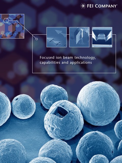
<strong>Focused</strong> <strong>ion</strong> <strong>beam</strong> <strong>technology</strong>,<br />
<strong>capabilities</strong> <strong>and</strong> applicat<strong>ion</strong>s<br />
1
<strong>Focused</strong> <strong>ion</strong> <strong>beam</strong> <strong>technology</strong>, <strong>capabilities</strong><br />
<strong>and</strong> applicat<strong>ion</strong>s<br />
A focused <strong>ion</strong> <strong>beam</strong> system (FIB) is a relatively new tool that has a high degree of analogy with a focused<br />
electron <strong>beam</strong> system such as a scanning electron microscope or a transmiss<strong>ion</strong> electron microscope.<br />
In these systems the electron <strong>beam</strong> is directed towards the sample, <strong>and</strong> upon interact<strong>ion</strong> it generates<br />
signals that are used to create high magnificat<strong>ion</strong> images of the sample. As the <strong>beam</strong> is well controlled in<br />
size <strong>and</strong> posit<strong>ion</strong> <strong>and</strong> the signals are strong enough to be detected without excessive noise, these kinds<br />
of tools are very powerful to analyze samples in great detail over a wide range of magnificat<strong>ion</strong>s.<br />
The major difference with a focused <strong>ion</strong> <strong>beam</strong><br />
system is the use of a different particle to create<br />
the primary <strong>beam</strong> that interacts with the sample.<br />
As the name FIB indicates, <strong>ion</strong>s are used instead of<br />
electrons.<br />
Figure 1: Ion <strong>beam</strong> induced SE image of a<br />
tungsten defect underneath an aluminum<br />
layer on a semi-conductor device.<br />
Figure 2: SE image (low current FIB) of an<br />
uncoated pollen grain, cut by the <strong>ion</strong> <strong>beam</strong><br />
(at high current).<br />
In a scanning electron microscope (SEM), electrons<br />
are accelerated <strong>and</strong> focused onto the sample<br />
surface. The <strong>beam</strong> can be scanned over the sample<br />
surface to create an image, or can be controlled<br />
by a patterning funct<strong>ion</strong> to locally expose the sample<br />
to the <strong>beam</strong>, as for example used in e-<strong>beam</strong><br />
lithography. These same basic funct<strong>ion</strong>alities are<br />
found in a focused <strong>ion</strong> <strong>beam</strong> system.<br />
Figure 3: Phase of TEM sample preparat<strong>ion</strong><br />
on a sample of a voided SiC composite<br />
material.<br />
3
Technology<br />
4<br />
Electrons replaced by <strong>ion</strong>s<br />
The most fundamental difference between SEM/TEM<br />
<strong>and</strong> FIB is the use of <strong>ion</strong>s <strong>and</strong> this has major consequences<br />
for the interact<strong>ion</strong>s that occur at the sample<br />
surface. A more detailed overview between electrons<br />
<strong>and</strong> <strong>ion</strong>s is given in the intermezzo. The most important<br />
characteristics <strong>and</strong> the consequences for the<br />
sample interact<strong>ion</strong> are:<br />
<strong>ion</strong>s are larger than electrons<br />
• Because <strong>ion</strong>s are much larger than electrons, they<br />
cannot easily penetrate within individual atoms of the<br />
sample. Interact<strong>ion</strong> mainly involves outer shell interact<strong>ion</strong><br />
resulting in atomic <strong>ion</strong>izat<strong>ion</strong> <strong>and</strong> breaking of<br />
chemical bonds of the substrate atoms. This is how<br />
secondary electrons <strong>and</strong> change of chemical state are<br />
created. Similarly inner shell electrons of the sample<br />
cannot be reached by the incoming <strong>ion</strong> <strong>and</strong> as a<br />
consequence inner shell excitat<strong>ion</strong> does not occur.<br />
Therefore, in contrast to the small electron that can<br />
easily penetrate in the electron cloud of the target<br />
atom there is no x-ray emiss<strong>ion</strong> when the sample is<br />
irradiated with an <strong>ion</strong> <strong>beam</strong>.<br />
• The large <strong>ion</strong> size also indicates that the probability<br />
of an interact<strong>ion</strong> with atoms from the sample is far<br />
higher, <strong>and</strong> as a consequence the <strong>ion</strong> rapidly loses its<br />
energy. The result is that the penetrat<strong>ion</strong> depth of the<br />
<strong>ion</strong>s is much lower than the penetrat<strong>ion</strong> of electrons<br />
of the same energy.<br />
• When the <strong>ion</strong> has come to a stop within the material,<br />
it is caught in the matrix of the material. Contrary to<br />
electrons that can disappear in the conductance b<strong>and</strong><br />
of the material, the <strong>ion</strong>s are trapped between the<br />
atoms of the sample, i.e. the sample is doped with<br />
Ga <strong>ion</strong>s roughly along the total penetrat<strong>ion</strong> depth of<br />
the <strong>beam</strong> for given energy <strong>and</strong> material.<br />
<strong>ion</strong>s are heavier than electrons<br />
• Because <strong>ion</strong>s are far heavier than electrons, <strong>ion</strong>s can<br />
gain a high momentum. For the same energy, the<br />
momentum of the <strong>ion</strong> is about 370 times larger. In<br />
the case where an electron collides with an atom,<br />
it can penetrate the electron cloud <strong>and</strong> reach the<br />
nucleus of the atom. Due to the strong nuclear forces<br />
the electron will be rejected, its velocity will be<br />
reversed, <strong>and</strong> the result is a high energy back scattered<br />
electron. As the electron mass is low compared to the<br />
mass of the sample atoms, the sample atom will<br />
hardly move at all (like a ping-pong ball hitting a<br />
football). When the <strong>ion</strong> hits an atom, its mass is<br />
comparable to the mass of the sample atom <strong>and</strong> as a<br />
consequence it will transfer a large amount of its<br />
momentum, i.e. the sample atom starts to move with<br />
a speed <strong>and</strong> energy high enough to remove it from its<br />
matrix (like a football hitting another football). The<br />
removal of atoms from their matrix is a phenomenon<br />
known as sputtering or milling. This elementary<br />
process works for all elements of the periodic table.<br />
The milling efficiency is typically a few um3 /nC <strong>and</strong> is<br />
higher for some materials <strong>and</strong> lower for others. The<br />
actual rate will depend on the mass of the target<br />
atom, its binding energy to the matrix <strong>and</strong> matrix<br />
orientat<strong>ion</strong> with respect to the incident direct<strong>ion</strong> of<br />
the <strong>beam</strong>.<br />
• For the same energy <strong>ion</strong>s move a lot slower than<br />
electrons. However, they are still fast compared to the<br />
image collect<strong>ion</strong> mode <strong>and</strong> in practice this has no real<br />
consequences (image shift of a few pixels taken into<br />
account). For highest speed milling, when the <strong>beam</strong><br />
moves around quickly including blanking, this effect<br />
is compensated in the instrument.<br />
• In both SEM <strong>and</strong> TEM magnetic lenses are used to<br />
focus the <strong>beam</strong>. As <strong>ion</strong>s are far heavier <strong>and</strong> therefore<br />
move slower, the corresponding Lorenz force is lower.<br />
The magnetic lenses are thus less effective on <strong>ion</strong>s<br />
than they would be on electrons with the same energy.<br />
As a consequence the focused <strong>ion</strong> <strong>beam</strong> system is<br />
equipped with electro-static lenses <strong>and</strong> not with<br />
magnetic lenses.<br />
<strong>ion</strong>s are positive <strong>and</strong> electrons are negative<br />
• This difference has negligible consequences <strong>and</strong> is<br />
taken care of by the polarity of fields to control the<br />
<strong>beam</strong> <strong>and</strong> accelerate the <strong>ion</strong>s.<br />
• The sign of the particle is only relevant when discussing<br />
charging phenomena on isolating samples but<br />
to underst<strong>and</strong> it, all generated charged particles must<br />
be taken into account. As shown in the table, the<br />
following particles leave the sample when irradiated<br />
with <strong>ion</strong>s: neutral atoms, positive <strong>and</strong> negative <strong>ion</strong>s,
FIB SEM Ratio<br />
Particle type Ga+ <strong>ion</strong> electron<br />
elementary charge +1 -1<br />
particle size 0.2 nm 0.00001 nm 20.000<br />
mass 1.2 .10-25 kg 9.1.10-31 kg 130.000<br />
velocity at 30 kV 2.8.105 m/s 1.0 108 m/s 0.0028<br />
velocity at 2 kV 7.3.104 m/s 2.6.107 m/s 0.0028<br />
momentum at 30 kV 3.4.10-20 kgm/s 9.1.10-23 kgm/s 370<br />
momentum at 2 kV 8.8.10-21 kgm/s 2.4.10-23 kgm/s 370<br />
Beam size nm range nm range<br />
energy up to 30 kV up to 30 kV<br />
current pA to nA range pA to uA range<br />
Penetrat<strong>ion</strong> depth In polymer at 30 kV 60 nm 12000 nm<br />
In polymer at 2 kV 12 nm 100 nm<br />
In iron at 30 kV 20 nm 1800 nm<br />
In iron at 2 kV 4 nm 25 nm<br />
Average electrons<br />
signal per 100<br />
secondary electrons 100 - 200 50 - 75<br />
particles at 20 kV back scattered electron 0 30 - 50<br />
substrate atom 500 0<br />
secondary <strong>ion</strong> 30 0<br />
x-ray 0 0.7<br />
<strong>and</strong> electrons. On average a<br />
completely isolating sample such as<br />
glass will charge up positively<br />
because of the incoming positive<br />
<strong>ion</strong> AND the outgoing negative<br />
secondary electrons. This charge<br />
build-up can be compensated by an<br />
addit<strong>ion</strong>al, in-chamber low energy<br />
electron gun that sprays electrons<br />
over the surface.<br />
In summary, <strong>ion</strong>s are positive, large,<br />
heavy <strong>and</strong> slow whereas electrons<br />
are negative, small, light <strong>and</strong> fast.<br />
The most important consequence of<br />
the properties listed above is that <strong>ion</strong><br />
<strong>beam</strong>s will remove atoms from the<br />
substrate <strong>and</strong> because the <strong>beam</strong><br />
posit<strong>ion</strong>, dwell time <strong>and</strong> size are so<br />
well controlled it can be applied to<br />
remove material locally in a highly<br />
controlled manner, down to the<br />
nanometer scale.<br />
The choice of Ga + <strong>ion</strong>s<br />
As a source, Ga + <strong>ion</strong>s are used in a FIB<br />
for various reasons:<br />
• The element Ga is metallic <strong>and</strong> has<br />
a low melting temperature <strong>and</strong><br />
hence it is a very convenient<br />
material to construct a compact<br />
gun with limited heating. The Ga<br />
can be contained in a very small<br />
volume so the gun has a long<br />
practical life-time. During operat<strong>ion</strong><br />
the gallium is in a liquid phase, <strong>and</strong><br />
so the source is referred to as a<br />
liquid metal <strong>ion</strong> source (LMIS)<br />
• A high brightness is obtained due<br />
to the surface potential, the flow<br />
properties of the Ga, the sharpness<br />
of the tip, <strong>and</strong> the construct<strong>ion</strong> of<br />
the gun which results in both<br />
<strong>ion</strong>izat<strong>ion</strong> <strong>and</strong> field emiss<strong>ion</strong>. This<br />
result is essential for the focused<br />
<strong>ion</strong> <strong>beam</strong>. Although other materials<br />
such as Ar (gas) can in theory also<br />
be used, the brightness of such a<br />
gun would be far lower <strong>and</strong> a Ar<br />
focused <strong>beam</strong> of the same size<br />
would not be very intense. Note<br />
that whatever material is chosen, it<br />
needs to be (singly) <strong>ion</strong>ized prior to<br />
<strong>beam</strong> format<strong>ion</strong> <strong>and</strong> then accelera-<br />
A more detailed comparison<br />
between FIB <strong>and</strong> SEM is given in<br />
this table. The comparison includes<br />
particles, <strong>beam</strong>s <strong>and</strong> signals.<br />
Some of the figures are averages<br />
<strong>and</strong> only serve as a guideline to<br />
get a feeling for the relevant<br />
scale. This is because the actual<br />
value is dependent on the materials<br />
involved. The basic interact<strong>ion</strong><br />
of a focused <strong>ion</strong> <strong>beam</strong> with atoms<br />
from the sample <strong>and</strong> hence the<br />
basic <strong>capabilities</strong> that such a <strong>technology</strong><br />
can offer can be understood<br />
from the values in the table.<br />
ted. FIB require a high brightness<br />
whereas, for example in the cleaning<br />
of <strong>ion</strong> flood guns, the current<br />
is more important <strong>and</strong> the actual<br />
source size is not relevant.<br />
• The element Ga is nicely posit<strong>ion</strong>ed<br />
in the center of the periodic table<br />
(element number 31) <strong>and</strong> its<br />
momentum transfer capability is<br />
optimal for a wide variety of materials.<br />
A lighter element such as Li<br />
would be less sufficient in milling<br />
heavier elements.<br />
• A consequence of the choice of Ga<br />
is that this element will always be<br />
present in the sample after exposure<br />
(dopant). The depth of the<br />
penetrat<strong>ion</strong> is shown in the intermezzo,<br />
<strong>and</strong> by x-ray analysis this<br />
element is easily traced back as its<br />
K-lines are nicely separated from<br />
other elements <strong>and</strong> hardly overlap<br />
with other L lines. In other words:<br />
the analytical interference of the<br />
element Ga is very low.<br />
5
6<br />
Useful signals<br />
As many signals are generated simultaneously, they<br />
may be used for detect<strong>ion</strong>, if efficient detect<strong>ion</strong> is possible.<br />
In this way all charged particles can be used as an<br />
imaging signal source, but the many neutral atoms are<br />
not used. Instead, these neutrals are the main component<br />
in the sputtering process <strong>and</strong> they are removed by<br />
the pumping system. Depending on the condit<strong>ion</strong>s,<br />
some of the neutrals may redeposit close to the area of<br />
milling. The charged particles, both <strong>ion</strong>s <strong>and</strong> electrons,<br />
can be used as an imaging signal. Since the <strong>ion</strong> <strong>beam</strong><br />
can be highly focused <strong>and</strong> scanned over the area it can<br />
be applied to create images at high magnificat<strong>ion</strong>. Note<br />
that the milling process itself continues during imaging<br />
but at a very low rate, because small spots <strong>and</strong> low<br />
<strong>beam</strong> currents are used for this. Although the top layer<br />
is removed continuously with every scan during imaging,<br />
in practice it is negligible in many cases. Another<br />
advantage of this gradual low rate milling is that the<br />
sample is “continuously cleaned” during imaging.<br />
The particles emitted from the surface during the irradiat<strong>ion</strong><br />
with the <strong>ion</strong> <strong>beam</strong> are schematically shown in<br />
Figure 5.<br />
Figure 4: The Ga liquid metal <strong>ion</strong> source, including<br />
the reservoir.<br />
If the sample materials matrix has different alignments,<br />
as in a multi-crystal phase, <strong>ion</strong>s may have a much<br />
higher or lower channeling yield depending on the<br />
local crystallographic orientat<strong>ion</strong>. As the <strong>ion</strong> is much<br />
larger than the electron, the sensitivity for the “projected<br />
atom compactness” is far higher. This phenomena,<br />
known as <strong>ion</strong> channeling, can be used to study the<br />
local differences in crystal orientat<strong>ion</strong>. It is also possible<br />
to use the (secondary) <strong>ion</strong> signal itself to create an<br />
image <strong>and</strong> in for example crystallography materials<br />
such as metals it will produce an excellent addit<strong>ion</strong>al<br />
contrast that shows the different grains of the material.<br />
The contrast of the <strong>ion</strong> signal can be different from the<br />
SE contrast (channeling, voltage contrast) <strong>and</strong> therefore<br />
<strong>ion</strong> imaging can give addit<strong>ion</strong>al informat<strong>ion</strong>.<br />
Although the majority of atoms emitted from the<br />
sample are not used, the emitted <strong>ion</strong>s can be used. In<br />
principle it is possible to analyze <strong>ion</strong>s <strong>and</strong> determine<br />
species <strong>and</strong> quantities by secondary <strong>ion</strong> mass spectroscopy<br />
(SIMS). In this way elemental distribut<strong>ion</strong>s are<br />
revealed during the milling of a sample, so in the third<br />
dimens<strong>ion</strong> as well.<br />
Substrate atoms<br />
milled from sample<br />
Collis<strong>ion</strong> with<br />
substrate atoms<br />
Ga + implantat<strong>ion</strong><br />
Incident Ga + Beam<br />
Figure 5: Interact<strong>ion</strong>s of the <strong>ion</strong> <strong>beam</strong> with the sample surface. The<br />
unique control offered by <strong>beam</strong> currents <strong>and</strong> spot sizes allow use<br />
of the FIB for both nano engineering as well as for high resolut<strong>ion</strong><br />
imaging using secondary electrons as well as <strong>ion</strong>s.<br />
<strong>ion</strong><br />
10 nm<br />
Secondary electron<br />
<strong>ion</strong>izat<strong>ion</strong>
Figure 6: High-resolut<strong>ion</strong> SE image by <strong>ion</strong> <strong>beam</strong> scanning of a gold<br />
on carbon sample. Also note the strong crystal grain contrast within<br />
the gold particles. Horizontal field width is 1.5 µm.<br />
FIB <strong>and</strong> SEM instrumentat<strong>ion</strong><br />
As electrons <strong>and</strong> <strong>ion</strong>s are both charged<br />
particles, a focused <strong>ion</strong> <strong>beam</strong> system<br />
<strong>and</strong> an electron <strong>beam</strong> system such as<br />
a SEM have much in common:<br />
vacuum, lens control, electronics,<br />
scanning <strong>and</strong> patterning facility,<br />
electron detect<strong>ion</strong>, PC control, stage,<br />
etc. The instruments therefore have a<br />
similar design as is shown in figure 8.<br />
Some important differences in the<br />
design of FIB <strong>and</strong> SEM are:<br />
• Continuous use of a blanking signal<br />
for the <strong>ion</strong> <strong>beam</strong> column, when the<br />
<strong>beam</strong> is not used to collect an<br />
image or to induce the milling<br />
process. This is completely interlocked<br />
<strong>and</strong> automated with the<br />
control of the system to prevent<br />
undesired milling (e.g. during<br />
imaging). For the SEM this kind of<br />
funct<strong>ion</strong>ality is mostly applied only<br />
for e-<strong>beam</strong> lithography when<br />
unwanted exposure of e-<strong>beam</strong> resist<br />
must be avoided.<br />
• Control of the <strong>beam</strong> current in a<br />
SEM is done by selecting different<br />
demagnificat<strong>ion</strong> factors (lens control)<br />
for the column (changing the<br />
size of the <strong>beam</strong> at the posit<strong>ion</strong> of<br />
the aperture). Control of the <strong>ion</strong><br />
<strong>beam</strong> current is realized by selecting<br />
different apertures (changing<br />
the size of the aperture at a fixed<br />
posit<strong>ion</strong> in the <strong>beam</strong>). For the <strong>ion</strong><br />
<strong>beam</strong> each of the selected apertures<br />
has an optimized performance at a<br />
certain lens setting <strong>and</strong> therefore,<br />
the more apertures, the more optimized<br />
the system will behave over<br />
the full <strong>beam</strong> current range.<br />
• The milling aspects of the FIB are<br />
so important that patterning is a<br />
st<strong>and</strong>ard capability of the system.<br />
For a SEM, patterning is mainly<br />
added for the sake of e-<strong>beam</strong> lithography.<br />
• The type of detectors that can be<br />
applied: SEM <strong>and</strong> FIB both have a<br />
Figure 7: Ion image of a chromium coated steel wire, showing very strong<br />
contrast of the metallic grains, due to their orientat<strong>ion</strong>s.<br />
secondary electron detector, SEM<br />
may have a back scatter electron<br />
detector, a STEM detector <strong>and</strong> /or<br />
an x-ray detector, whereas FIB has<br />
an <strong>ion</strong> detector. Both systems can<br />
also use the sample current as a<br />
signal.<br />
• FIB can be equipped with an <strong>ion</strong><br />
flood gun to greatly reduce the<br />
charging of insulating samples.<br />
As can be derived from the intermezzo,<br />
the charging induced by the<br />
<strong>ion</strong> <strong>beam</strong> is positive <strong>and</strong> any addit<strong>ion</strong>al<br />
negative charge can be used<br />
to compensate this. One way that<br />
conveniently compensates the<br />
charge is the use of a flood gun: a<br />
low-energy, non focused spray of<br />
electrons that compensates the<br />
positive charge on the surface.<br />
7
8<br />
Anode<br />
Lens 1<br />
Scan &<br />
Stig Coils<br />
Electron<br />
Beam<br />
Electron<br />
Beam<br />
impact<br />
area<br />
Turbo/<br />
diff pump<br />
E-Beam Ion-Beam<br />
E source<br />
Gun<br />
align coils<br />
Lens 2<br />
Lens 3<br />
Final<br />
lens body<br />
Collector<br />
system<br />
Secondary<br />
electrons<br />
Roughing<br />
line (to<br />
rotary etc...)<br />
Figure 9: Graph indicating the usefulness of the many apertures in the <strong>ion</strong> column, so that for<br />
various <strong>ion</strong> <strong>beam</strong> settings the system can always be optimized by selecting the proper<br />
aperture.<br />
Figure 10: SE image induced by <strong>ion</strong> <strong>beam</strong> of<br />
isolated bond pad on an IC device. Structures<br />
are masked by strong contrast <strong>and</strong> chargelines.<br />
Extractor<br />
Lens 1<br />
Blanking<br />
plates<br />
Lens 2<br />
Octopole<br />
for stigs,<br />
scan etc...<br />
Impact area<br />
of Ion Beam<br />
Sample<br />
Turbo<br />
pump<br />
Ga + LMI source<br />
Suppresser<br />
Octopole<br />
alignment<br />
Blanking<br />
aperture<br />
Continuous<br />
dinode<br />
detector<br />
Electrons<br />
or <strong>ion</strong>s imaging<br />
Roughing<br />
line (to<br />
rotary etc...)<br />
Figure 8: Schematic presentat<strong>ion</strong> of SEM <strong>and</strong> FIB <strong>and</strong> the many similarities of the instruments.<br />
Figure 11: Ion image of the same structure.<br />
This also shows strong charging of the sample<br />
prohibiting a good view of the sample.<br />
Figure: 12 Ion image but now recorded with<br />
flood gun on. The spray of electrons has<br />
eliminated the charge build-up <strong>and</strong> details<br />
become apparent.
Capabilities of the focused <strong>ion</strong> <strong>beam</strong> system<br />
Apart from the superb FIB imaging <strong>capabilities</strong> obtained by regular scanning of the (low current)<br />
<strong>ion</strong> <strong>beam</strong>, the system can also translate a pattern of doses onto the sample <strong>and</strong> induce active <strong>and</strong><br />
controlled surface milling.<br />
Milling<br />
As is shown by the basic interact<strong>ion</strong><br />
of the <strong>ion</strong> <strong>beam</strong> with the sample,<br />
milling is a continuous process that<br />
always occurs during <strong>beam</strong> exposure.<br />
The milling process as such is an<br />
atomic collis<strong>ion</strong> process. The milling<br />
rate (µm3 /s) is (linear) proport<strong>ion</strong>al to<br />
the <strong>beam</strong> current <strong>and</strong> high amounts<br />
of material are removed with high<br />
<strong>beam</strong> currents. In addit<strong>ion</strong>, precise<br />
control is possible by the use of<br />
smaller spot sizes <strong>and</strong> hence smaller<br />
currents. A typical rectangular area of<br />
10 x 5 x 3 µm can take around 10<br />
minutes for complete removal. As the<br />
<strong>ion</strong> <strong>beam</strong> posit<strong>ion</strong> is well controlled,<br />
milling can be used to create a simple<br />
structure such as a square or round<br />
hole in the material, but also a more<br />
complex pattern as shown below.<br />
3.1 µm<br />
Figure 13: Image of a direct write <strong>ion</strong> <strong>beam</strong><br />
nano-pattern in gold. Time to result is 8<br />
minutes. Milling of complex patterns <strong>and</strong><br />
arbitrary shapes defined in bitmaps are a<br />
basic funct<strong>ion</strong> of the system.<br />
Milling is the most powerful capability<br />
of the focused <strong>ion</strong> <strong>beam</strong> <strong>and</strong><br />
directly related to the choice of <strong>ion</strong>,<br />
its energy range <strong>and</strong> the momentum<br />
of the particle (its weight). Milling<br />
allows the freedom to manipulate the<br />
sample, open it up in the third<br />
dimens<strong>ion</strong> <strong>and</strong> create a cross-sect<strong>ion</strong>,<br />
or to create any possible shape as<br />
“carved in stone”. Not only the lateral<br />
posit<strong>ion</strong>, but also the local depth<br />
can be controlled. In this way milling<br />
is different from etching with a mask<br />
on the sample.<br />
Removal of atoms from the surface<br />
can be enhanced by the addit<strong>ion</strong> of<br />
local chemistry in the form of a gas<br />
delivery system. This local supply of<br />
gas can, for example, change the oxidat<strong>ion</strong><br />
of released particles <strong>and</strong> may<br />
Figure 14: Example of a cross-sect<strong>ion</strong> imaged<br />
<strong>and</strong> made by the FIB. The cross-sect<strong>ion</strong><br />
shows an insulat<strong>ion</strong> defect on a semi-conductor<br />
device.<br />
substantially speed up the milling<br />
process. In general it will also reduce<br />
the local re-deposit<strong>ion</strong> of atoms<br />
released from the surface. Examples<br />
of gases that are used to enhance<br />
milling are I2 <strong>and</strong> XeF2. Figure 15: Silicon surface showing both<br />
milling <strong>and</strong> deposit<strong>ion</strong> <strong>capabilities</strong> as examples<br />
of the creat<strong>ion</strong> of local structures. A, B,<br />
C <strong>and</strong> D are micro-deposit<strong>ion</strong>s, whereas E, F<br />
<strong>and</strong> G are structures milled into the sample.<br />
Figure 16: In-situ foil extract<strong>ion</strong> using micromanipulators<br />
in the chamber. The next stage<br />
is that the TEM lamella shown on the tip is<br />
deposited on a TEM grid, or “micro-welded”<br />
onto a support ring that fits in the TEM.<br />
9
10<br />
Deposit<strong>ion</strong><br />
As FIB <strong>technology</strong> is frequently used for milling an<br />
addit<strong>ion</strong>al technique can convert the <strong>ion</strong> <strong>beam</strong> system<br />
into a deposit<strong>ion</strong> system allowing the addit<strong>ion</strong> of material<br />
instead of removing material. This is realized by<br />
adding a so-called gas delivery system, that locally<br />
supplies a chemical compound close to the surface<br />
impact point. The chemical gas compound often<br />
consists of a organic-metallic molecule such as methyl<br />
cyclo pentadienyl Pt (IV) tri methyl. When this compound<br />
is exposed to the <strong>ion</strong> <strong>beam</strong> it will decompose<br />
locally <strong>and</strong> deposit Pt onto the surface. In general the<br />
cracking of the molecule is not 100% so there are<br />
always some addit<strong>ion</strong>al matrix molecules such as organic<br />
residues that are also deposited. The purity of the<br />
deposit is therefore generally lower compared to, for<br />
example, CVD deposits. The main advantage in comparison<br />
to CVD or PVD is the highly local deposit<strong>ion</strong>,<br />
<strong>and</strong> the capability to create different heights of the<br />
deposit in one exposure. In addit<strong>ion</strong> the direct deposit<strong>ion</strong><br />
capability is flexible <strong>and</strong> does not require complex<br />
mask structures.<br />
Molecules are absorbed on the irradiated area, <strong>and</strong> by<br />
using the patterning capability of the system three<br />
dimens<strong>ion</strong>al structures can be grown at selected posit<strong>ion</strong>s,<br />
with full control of size, posit<strong>ion</strong> <strong>and</strong> height.<br />
So this capability is a very welcome addendum to the<br />
FIB’s milling power. The material deposited depends on<br />
the gas chemistry used <strong>and</strong> various opt<strong>ion</strong>s are possible.<br />
Readily available gas chemistry allows the deposit<strong>ion</strong> of<br />
Pt, W, SiO2, C.<br />
Figure 17: Light microscope image of the sample deposited ex-situ<br />
on a TEM grid. Ex-situ foil extract<strong>ion</strong> using electro-static probes<br />
works even for materials with low structural integrity.<br />
Important characteristics for the deposit<strong>ion</strong>s are the<br />
minimum size (typically around 50 nm), the purity of<br />
the material, <strong>and</strong> its conductivity which is usually lower<br />
than the pure metal.<br />
Creat<strong>ion</strong> of TEM lamella<br />
An important capability, derived from the system’s<br />
milling capacity, is the creat<strong>ion</strong> of thin lamella that are<br />
transparent to an electron <strong>beam</strong> <strong>and</strong> hence can serve as<br />
a TEM sample. As the posit<strong>ion</strong> of the <strong>ion</strong> <strong>beam</strong> can be<br />
controlled to a high degree, the TEM lamella can be<br />
created at any locat<strong>ion</strong> that is of interest to the user.<br />
<strong>Focused</strong> <strong>ion</strong> <strong>beam</strong> machining for the creat<strong>ion</strong> of TEM<br />
samples is now firmly established as the most versatile<br />
<strong>and</strong> accurate method currently available. There are<br />
several ways to extract the FIB machined foil from the<br />
bulk sample without having to use mechanical preparat<strong>ion</strong><br />
at all, so for the first time it is not necessary to<br />
sacrifice the sample when performing TEM analysis<br />
with the highest accuracy.<br />
Site specific<br />
The fact that the locat<strong>ion</strong> of the foil site can be defined<br />
inside the FIB makes this the only true site-specific<br />
technique available. The momentary feed-back of what<br />
<strong>and</strong> where FIB milling takes place is essential to<br />
generate the best samples from the reg<strong>ion</strong> of interest.<br />
Lateral placement of foils is quite simple, <strong>and</strong> the aimed<br />
thickness is in the range of 100 nm <strong>and</strong> can be controlled<br />
to a high degree.<br />
Material independent<br />
As the <strong>ion</strong> <strong>beam</strong> removes atoms from the sample in an<br />
atomic collis<strong>ion</strong> process rather than with a mechanical<br />
bulk cut or mechanical polish, the amount of <strong>ion</strong>s<br />
needed to remove different materials with varying hardness<br />
is not related to the structure or the composit<strong>ion</strong><br />
of the sample. This means that milling any material or<br />
a combinat<strong>ion</strong> of materials is as straightforward as a<br />
simple single crystal sample for <strong>ion</strong> <strong>beam</strong> machining.<br />
Even voided, brittle or soft/hard combinat<strong>ion</strong>s of materials<br />
are easy for the FIB process. Many TEM samples<br />
that were difficult or impossible to make until now (soft<br />
polymer coating on metal, hard metal on soft metal)<br />
are now easy to make using FIB <strong>technology</strong>.
Automated <strong>and</strong> executed unattended<br />
<strong>FEI</strong> is the only company to offer a fully funct<strong>ion</strong>al <strong>and</strong><br />
integrated automatic TEM sample preparat<strong>ion</strong> capability.<br />
By combining image recognit<strong>ion</strong> software with the<br />
full software control of patterning, stage <strong>and</strong> <strong>beam</strong> posit<strong>ion</strong><br />
the process can be run automatically, even without<br />
operator presence.<br />
Multi-sites possible<br />
This funct<strong>ion</strong> can be extended to run overnight <strong>and</strong><br />
dozens of foils can be prepared automatically, providing<br />
a significant enhancement to instrument effectiveness<br />
not only for the FIB instrument but also for the TEM<br />
used in the subsequent analysis.<br />
Figure 18: Automated TEM sample preparat<strong>ion</strong> is now being used<br />
on a wide variety of materials with the highest success rate. This<br />
image shows a multi-site TEM sample preparat<strong>ion</strong> in olive rock,<br />
allowing many samples from posit<strong>ion</strong>s to be well-defined <strong>and</strong> close<br />
to each other. No other technique allows this high flexibility.<br />
Figure 19: TEM image of a FIB prepared foil showing a 12° Mg-silicate<br />
grain boundary in a synthetic bi-crystal. High quality foils from<br />
a wide variety of materials are straightforward <strong>and</strong> permit the most<br />
dem<strong>and</strong>ing TEM applicat<strong>ion</strong>s with all the benefits of FIB preparat<strong>ion</strong>.<br />
Mill Allignment Marks<br />
Figure 20: The 6 stages of automated TEM sample preparat<strong>ion</strong>.<br />
Micro <strong>and</strong> nano patterning<br />
Thin to < 1 µm<br />
Deposit Protective Layer Cut out Membrane<br />
Bulk Milling Final Thinning < 50 nm<br />
Control the specialized micro-structure fabricat<strong>ion</strong> with<br />
FIB as it delivers rapid three dimens<strong>ion</strong>al process control<br />
<strong>and</strong> hence reduces the product development cycle.<br />
As FIB has accurate control over milling parameters as<br />
well as over deposit<strong>ion</strong> parameters, it is the ideal tool to<br />
quickly create small structures in the top-down<br />
approach for nano-<strong>technology</strong>. It is a mask-less technique<br />
<strong>and</strong> highly flexible <strong>and</strong> fast for a serial technique.<br />
These qualities make FIB valuable for prototyping <strong>and</strong><br />
design modificat<strong>ion</strong>s.<br />
MEMS <strong>and</strong> NEMS prototyping<br />
If a prototype device does not fulfill its specificat<strong>ion</strong><br />
<strong>and</strong> is unable to deliver the right result, it can be directly<br />
modified with FIB until it does. The process <strong>technology</strong><br />
required to create 3D micro-structures is expensive,<br />
complex <strong>and</strong> can take months to perfect. By using the<br />
direct modificat<strong>ion</strong> <strong>capabilities</strong> of <strong>ion</strong> <strong>beam</strong> machining<br />
combined with instant deposit<strong>ion</strong> <strong>and</strong> etching<br />
chemistries, real results can be achieved while the<br />
11
12<br />
Figure 21: Cantilever with proof-mass<br />
machined from a Si 2N 3 membrane.<br />
Figure 22: Image of a spring, supporting the<br />
proof-mass of a MEMS accelerometer. The<br />
support spring has been weakened by <strong>ion</strong><br />
<strong>beam</strong> removal of half of the spring thickness.<br />
Figure 23: Image of the spring, that has now<br />
been strengthened with <strong>ion</strong> <strong>beam</strong> deposited<br />
SiO 2.<br />
Courtesy: “University of Birmingham, Research Centre<br />
for Micro Engineering <strong>and</strong> Nano-<strong>technology</strong>.<br />
Figure 24: Low magnificat<strong>ion</strong> SE image of a<br />
fungal infect<strong>ion</strong> in wood. This untreated<br />
sample was imaged at low magnificat<strong>ion</strong> <strong>and</strong><br />
low <strong>beam</strong> current for 30 minutes without<br />
noticeable deteriorat<strong>ion</strong>.<br />
manufacturing process matures. New<br />
product development can be ramped<br />
up <strong>and</strong> product introduct<strong>ion</strong> cycles<br />
shortened by including direct device<br />
customizat<strong>ion</strong> into the product<br />
development process. Demonstrate<br />
funct<strong>ion</strong>ing devices <strong>and</strong> debug your<br />
control systems while the product<strong>ion</strong><br />
process is fine-tuned. For example,<br />
change the spring constant of an<br />
accelerometer or simply create a new<br />
structure in <strong>and</strong> on a thin film.<br />
Optical MEMS<br />
Check the structure, the robustness<br />
<strong>and</strong> the failure mechanisms of optical<br />
devices. Monitor the applied<br />
process <strong>and</strong> maximize the yield for<br />
cost effective product<strong>ion</strong>.<br />
Routers, multiplexers, wave-guides<br />
<strong>and</strong> transmiss<strong>ion</strong> media all rely on<br />
exact dimens<strong>ion</strong>s for their performance.<br />
High aspect ratio microstructures<br />
provide convent<strong>ion</strong>al top down<br />
metrology solut<strong>ion</strong>s with unavoidable<br />
physical restrict<strong>ion</strong>s. Only by<br />
progressing to three-dimens<strong>ion</strong>al<br />
characterizat<strong>ion</strong> can a true underst<strong>and</strong>ing<br />
of the manufacturing performance<br />
be acquired.<br />
The metrology of wave-guides can be<br />
automated <strong>and</strong> process failures identified<br />
<strong>and</strong> eliminated before costly<br />
device yield is affected. The communicat<strong>ion</strong><br />
b<strong>and</strong>width requirements for<br />
optical devices are continuously<br />
increasing <strong>and</strong> therefore process control<br />
is becoming increasingly important.<br />
Now the device producer can<br />
switch to the enhanced control <strong>and</strong><br />
cost savings already enjoyed by the<br />
semiconductor industry.<br />
Figure 25: Image of a biopsy of bone material.<br />
The biopsy-to-be is completely created by<br />
FIB milling only.<br />
Figure 26: Bone material biopsy after extract<strong>ion</strong>.<br />
Figure 27: An AFM tip, CVD gold coated <strong>and</strong><br />
then FIB machined to remove the gold on the<br />
pyramid slope to leave only a gold tip at the<br />
point of surface contact. Different bio-materials<br />
can be grown here as they easily bind to<br />
the gold <strong>and</strong> the forces exerted on this specimen<br />
during subsequent interact<strong>ion</strong>s can be<br />
directly monitored.
Figure 28: SE images created by FIB of cross-sect<strong>ion</strong> through an<br />
optical wave guide product. The sample surface is first covered<br />
with a protective layer of Pt. The measurements shown in the<br />
image are obtained automatically using <strong>FEI</strong>’s IC3D metrology<br />
opt<strong>ion</strong>.<br />
Figure 29: TEM image of a foil machined by FIB from a strained silicon<br />
MOSFET device. The dark layer at the top is tungsten deposited<br />
as a protective sheet during the FIB sample preparat<strong>ion</strong>.<br />
Compound semi-conductor<br />
From the mainstream laser <strong>and</strong> fast response transistor<br />
applicat<strong>ion</strong>s to the more exotic blue/green or even<br />
white light emitting devices that exist only at the edge<br />
of what is currently possible, compound semiconductor<br />
devices are firmly established as one of the communicat<strong>ion</strong>s<br />
industries enabling technologies. 3-Dimens<strong>ion</strong>al,<br />
site-specific investigat<strong>ion</strong>s of complex thin films like<br />
laser facets, lifted directly from returned devices cans, is<br />
now a routine investigat<strong>ion</strong> technique.<br />
Device manufacturers utilizing materials as varied in<br />
their properties as GaN, SiGe, GaAs <strong>and</strong> InP now<br />
require routine fabricat<strong>ion</strong> process control. Researchers<br />
creating new types of device from more exotic materials<br />
like Cadmium <strong>and</strong> Selenium are now relying on the<br />
direct machining <strong>capabilities</strong> that only a FIB <strong>technology</strong><br />
can provide.<br />
Figure 30: Image of an optical fiber where a<br />
customized grating has been machined with<br />
FIB into the core to permit a single wavelength<br />
to be monitored in a multi-mode signal.<br />
Figure 31: SEM-STEM image of a<br />
GaAs/AlGaAs QW laser structure. The foil was<br />
prepared using FIB <strong>technology</strong>.<br />
13
Applicat<strong>ion</strong> examples<br />
14<br />
The New Dimens<strong>ion</strong> in<br />
Life Science<br />
Can an <strong>ion</strong> <strong>beam</strong> system be used on<br />
life science samples? Ion <strong>beam</strong><br />
microscopy for imaging, crosssect<strong>ion</strong>ing<br />
<strong>and</strong> 3D machining is a<br />
rapidly growing applicat<strong>ion</strong> area for<br />
biological research. Many of the<br />
convent<strong>ion</strong>al sample preparat<strong>ion</strong><br />
techniques used within life-sciences<br />
today, are directly compatible with<br />
investigat<strong>ion</strong> by the FIB.<br />
It is sometimes difficult to examine<br />
biological material in its natural state<br />
using any type of scanning or<br />
transmiss<strong>ion</strong> microscopy because of<br />
the vacuum compatibility of these<br />
samples. In order to circumvent this<br />
problem, biologists have developed<br />
many techniques to enable a sample<br />
to maintain many of its original<br />
qualities. Techniques such as chemical<br />
fixing, drying, <strong>and</strong> cryogenic<br />
preparat<strong>ion</strong> such as high pressure<br />
freezing have long been used as<br />
sample preparat<strong>ion</strong> techniques for<br />
these biological materials.<br />
Some of these prepared biological<br />
samples are robust enough to be used<br />
directly in the focused <strong>ion</strong> <strong>beam</strong> with<br />
the big advantage that site specific,<br />
3D investigat<strong>ion</strong>s become available to<br />
the life science researcher. Specimens<br />
with hard cell walls such as plants, or<br />
with an outer skeleton such as<br />
insects, <strong>and</strong> plant materials can even<br />
be applied in the FIB without any<br />
preparat<strong>ion</strong>.<br />
Also many other aspects related to<br />
life science research now benefit from<br />
<strong>ion</strong> <strong>beam</strong> applicat<strong>ion</strong>s. Directly<br />
machining growth media at the<br />
Micro-Nano scale for subsequent<br />
populat<strong>ion</strong> growth experiments, or<br />
micro-scale biopsies from bone are<br />
just 2 examples of indirect biological<br />
applicat<strong>ion</strong>s. AFM tips with bio active<br />
materials deposited onto the contact<br />
point allow for addit<strong>ion</strong>al biological<br />
informat<strong>ion</strong> such as parameters for<br />
the metabolism in a biological system.<br />
Another example may be the<br />
real-time measurement of forces present<br />
during interact<strong>ion</strong>s between<br />
living species.<br />
Micro-biopsy from hard materials can<br />
now be performed on the micro-scale.<br />
Figures 25 <strong>and</strong> 26 show a petrified<br />
bone sample undergoing a biopsy <strong>and</strong><br />
extract<strong>ion</strong> with a block of material<br />
removed which is only 10 microns<br />
wide; this block can be used for DNA<br />
replicat<strong>ion</strong>, chemical analysis, or can<br />
be thinned into a TEM sample. With<br />
only a few microns of material<br />
removed <strong>and</strong> no mechanical sample<br />
preparat<strong>ion</strong> required, detailed analysis<br />
of biological samples can be done<br />
without sacrificing the integrity of<br />
the original specimen.<br />
Pollen imaging <strong>and</strong> cutting process is<br />
shown in the figures 34-36. The<br />
process steps were: stamen removed<br />
from flower, pollen tapped onto double<br />
sided carbon tape, pollen residue<br />
removed with an air gun, loaded in<br />
the chamber, cross-sect<strong>ion</strong>ed <strong>and</strong><br />
then images were produced, all with<br />
a process time of only 20 munutes.<br />
Figure 32: SE image made with FIB of uncoated<br />
bee antennae.<br />
Figure 33: Bacterial PTFE growth-media<br />
modified by <strong>ion</strong> <strong>beam</strong> milling <strong>and</strong> <strong>ion</strong> <strong>beam</strong><br />
induced metal deposit<strong>ion</strong>.<br />
Figure 34: Natural, unprepared pollen grains<br />
shown by SE imaging with the FIB.<br />
Figure 35: Top down secondary electron<br />
image of one pollen grain, cross-sect<strong>ion</strong>ed by<br />
the <strong>ion</strong> <strong>beam</strong>.
Figure 36: Secondary <strong>ion</strong> image of an uncoated<br />
pollen grain tilted 45°. The cross-sect<strong>ion</strong><br />
itself was made with the same <strong>beam</strong>, but at<br />
a higher <strong>beam</strong> current.<br />
Nano<strong>technology</strong>: the shape of things<br />
to come<br />
The commercializat<strong>ion</strong> of nano-science is limited by the<br />
available tools – the use of a focused <strong>ion</strong> <strong>beam</strong> system<br />
delivers site specific imaging <strong>and</strong> fabricat<strong>ion</strong> <strong>capabilities</strong><br />
that strongly reduce the development <strong>and</strong> characterizat<strong>ion</strong><br />
cycles dem<strong>and</strong>ed by scientists in nano-<strong>technology</strong>.<br />
FIB <strong>capabilities</strong> are highly valuable for rapid prototyping.<br />
As a consequence products <strong>and</strong> profits are brought<br />
more rapidly to the nano<strong>technology</strong> industry.<br />
Nano-particles as catalysts <strong>and</strong> active media in<br />
fuel cells<br />
If there is a need to find out what an active material is<br />
Figure 39: Ion <strong>beam</strong> deposited tungsten<br />
nano-wires for direct electrical measurements<br />
(4 point probe) of nano structures, in this<br />
case a carbon nanotube.<br />
Figure 37: Bright field TEM image showing<br />
the locat<strong>ion</strong> of the platinum group material<br />
deposit at the vertical interface. Locat<strong>ion</strong><br />
proven by EELS mapping (insert showing<br />
the Pt posit<strong>ion</strong> in blue).<br />
Figure 40: SEM image of a FIB machined<br />
single electron nano-bridge in a super-conducting<br />
film. The FIB can even be configured<br />
for dynamic electrical measurements at liquid<br />
helium temperatures during FIB milling.<br />
Figure 38: Customized SNOM tip made with FIB.<br />
doing at a single point in the support matrix, you can<br />
go straight to it <strong>and</strong> find out. Site-specific TEM sample<br />
preparat<strong>ion</strong> of chemical deposits embedded in porous<br />
ceramic media is now no more difficult than polishing a<br />
sample before examining it. Materials independent, sitespecific<br />
TEM samples can be prepared automatically<br />
from any site identified by any technique.<br />
Figure 41 is an EDS map localizat<strong>ion</strong> of a platinum<br />
group material deposit on an internal surface of a ceramic<br />
matrix. The matrix has been injected with a vacuum<br />
proof resin for structural stability. Once the area of interest<br />
is found, the specimen is cut <strong>and</strong> extracted without<br />
breaking the sample. The final step is transfer to a TEM<br />
grid followed by highly detailed (S)TEM analysis.<br />
Figure 41: EDS map showing distribut<strong>ion</strong> of<br />
platinum group deposits within a catalyst<br />
support matrix. The color represents the<br />
relative WT % Pt.<br />
15
16<br />
Figure 42: FIB machined photonic array with<br />
customized pitch. 30 micron field of view.<br />
Time to product<strong>ion</strong> is 15 minutes.<br />
Figure 45: SE image made with the low current<br />
<strong>ion</strong> <strong>beam</strong>, showing a piezoelectric<br />
Lithium Niobate tip with FIB deposited electrodes<br />
<strong>and</strong> connect<strong>ion</strong>s.<br />
AFM (SPM)<br />
If the st<strong>and</strong>ard methods of nano-device<br />
research are no longer applicable,<br />
the rules can be changed <strong>and</strong> the<br />
toolset customized for the new<br />
challenges ahead. Scanning probe<br />
microscopes rely on the characteristics<br />
of the probes they use. This<br />
single part of an AFM (SPM) has not<br />
changed a lot since the technique<br />
was invented. By harnessing the ability<br />
of focused <strong>ion</strong> <strong>beam</strong> techniques to<br />
customize all the characteristics of<br />
the tips individually, the true <strong>capabilities</strong><br />
of AFM can be used for the<br />
first time.<br />
It is now possible to change the tip<br />
profile, the tip material, or the tip<br />
conductivity to allow it to measure<br />
Figure 43: Image of a sapphire tip sharpened<br />
locally by FIB milling. This ‘Super tip’ on the<br />
tip is extremely sharp, as is shown by comparing<br />
the two radii.<br />
the data you need.<br />
Instead of measuring the topography<br />
of the surface, measure the forces<br />
exerted during a catalytic react<strong>ion</strong>, or<br />
the attract<strong>ion</strong> between magnetic<br />
domains, or the effects of applying a<br />
voltage to an individual muscle fiber.<br />
The ability to rapidly adapt <strong>and</strong><br />
innovate is distilled into one single<br />
instrumental solut<strong>ion</strong>. The FIB will<br />
exp<strong>and</strong> the <strong>capabilities</strong> of the AFM<br />
by allowing customized tip modificat<strong>ion</strong><br />
that suits to discover the informat<strong>ion</strong><br />
required. An example is a<br />
modificat<strong>ion</strong> of the light emitting tip<br />
of the scanning near-field optical<br />
microscope, one of the variants of<br />
the AFM.<br />
Structural Nano-Prototyping<br />
Creating structures at the micro to<br />
nano scale relies on processes that<br />
operate with the tightest control<br />
st<strong>and</strong>ards. To underst<strong>and</strong> whether<br />
the behavior of a structure within a<br />
certain environment is attributable to<br />
its chemistry, its electrical or magnetic<br />
characteristics, its dynamic behavior<br />
or even just its shape can be<br />
challenging <strong>and</strong> time consuming.<br />
The structure itself may not be trivial<br />
Figure 44: SE image made with FIB showing a<br />
silicon AFM tip machined to be a super-tip,<br />
with very small radius for high resolut<strong>ion</strong><br />
AFM imaging.<br />
to create, <strong>and</strong> underst<strong>and</strong>ing the<br />
failure modes of unique sites seems<br />
impossible using convent<strong>ion</strong>al techniques.<br />
The direct etch/deposit<strong>ion</strong><br />
combinat<strong>ion</strong> of FIB combined with<br />
its digitally addressed patterning<br />
system provides a nano-prototyping<br />
engine with exciting new <strong>capabilities</strong><br />
to assist the researcher in nano<br />
<strong>technology</strong>. In fact, the focused <strong>ion</strong><br />
<strong>beam</strong> system operates at micro <strong>and</strong><br />
nano scale <strong>and</strong> hence can also be<br />
used to actually create the structures<br />
required, in addit<strong>ion</strong> to its analytical<br />
capability. New higher precis<strong>ion</strong><br />
control <strong>and</strong> structural analysis have<br />
become a new routine using FIB.<br />
Figure 46: Optical image of the extracted<br />
TEM foil on a TEM grid. The vertical interface<br />
between resin <strong>and</strong> ceramic matrix is clearly<br />
visible.
Figure 47: SE image of Pt group material. TEM lamella in preparat<strong>ion</strong>.<br />
Imaging with FIB perpendicular to the surface.<br />
Industrial Process Solut<strong>ion</strong>s<br />
The length of time it takes to confirm that a fabricat<strong>ion</strong><br />
process works normally or, more importantly, to underst<strong>and</strong><br />
the reasons why it is not working properly, has a<br />
price. It can be measured in lost product<strong>ion</strong>, in customer<br />
purchasing confidence <strong>and</strong> in simple product funct<strong>ion</strong>ality.<br />
Minimizing the period of uncertainty means cost<br />
savings, <strong>and</strong> spending money to save money is the easiest<br />
way to drive innovat<strong>ion</strong> <strong>and</strong> boost competitiveness.<br />
The rapid 3D analysis <strong>capabilities</strong> <strong>and</strong> the direct applicability<br />
<strong>and</strong> robustness of the FIB technique lends itself<br />
uniquely to industrial applicat<strong>ion</strong>s. Sample preparat<strong>ion</strong><br />
for FIB limits itself to ensuring the sample can withst<strong>and</strong><br />
the vacuum in the chamber. Sometimes samples for<br />
microscopy need to be cleaned up to remove an oxide<br />
layer or a hydro-carbon contaminat<strong>ion</strong> on top. For FIB<br />
these layers can be removed in-situ by the <strong>beam</strong> itself,<br />
avoiding any preparat<strong>ion</strong> of this kind. These processes are<br />
only done locally at the site of the analysis leaving the<br />
rest of the sample in its original state, <strong>and</strong> this can be<br />
useful for other subsequent tests.<br />
FIB <strong>technology</strong> already assists industrial research in many<br />
leading analysis laboratories:<br />
• within nuclear research for the ability to analyze <strong>and</strong><br />
manipulate samples<br />
• without any mechanical preparat<strong>ion</strong><br />
• within the polymer industry for artifact-free nonmechanical<br />
3D investigat<strong>ion</strong>s<br />
• within the metallurgy industry for zero damage inspec-<br />
t<strong>ion</strong> of corros<strong>ion</strong> products, grain informat<strong>ion</strong> well below<br />
1µm <strong>and</strong> true 3D surface coating analysis<br />
• within composite materials manufacturing because of<br />
the ability to image <strong>and</strong> cut materials with different<br />
hardness with zero artifacts<br />
• within the ceramics industry for 3D analysis <strong>and</strong> ease of<br />
h<strong>and</strong>ling of hard, insulating materials.<br />
The results shown in this brochure are from metallurgy<br />
samples, composite samples <strong>and</strong> polymer samples, each<br />
showing FIB 3D cross-sect<strong>ion</strong> analysis or TEM sample<br />
preparat<strong>ion</strong> of a specific failure site, <strong>and</strong> each was done in<br />
less than one hour. Ion <strong>beam</strong> cross-sect<strong>ion</strong>ing can also be<br />
done both laterally <strong>and</strong> transversely at the same locat<strong>ion</strong>,<br />
even on the same sub-micron feature, providing a level<br />
of immediate, site-specific informat<strong>ion</strong> that is just not<br />
available with any other technique.<br />
Figure 48: FIB cross-sect<strong>ion</strong> through an uncoated bi-phase polymer.<br />
This shows a mixing process failure in the molded polymer product.<br />
Insert: detailed view showing separat<strong>ion</strong> of polymer phases around<br />
air pockets.<br />
17
18<br />
Figure 49: SE image made with <strong>ion</strong> <strong>beam</strong> of<br />
catalyst covered ceramic balls. The use of FIB<br />
allows any individual particle to be selected<br />
<strong>and</strong> analyzed for industrial quality control. In<br />
this case the FIB has machined a TEM sample<br />
of the top surface. Time to result: 60 minutes.<br />
FIB systems deliver a single instrumental solut<strong>ion</strong> to enhance the speed <strong>and</strong> quality of the IC product<strong>ion</strong> process. The capability to perform<br />
design edits to the fabricated circuit ensures that the design <strong>and</strong> debug phase is limited to one mask step, <strong>and</strong> that extensive <strong>and</strong> expensive<br />
iterat<strong>ion</strong> steps can be avoided. The process control <strong>and</strong> failure analysis <strong>capabilities</strong> offered by FIB also provide the fastest possible route-cause<br />
data to shorten yield improvement cycles <strong>and</strong> solve site specific failure modes, either in the product<strong>ion</strong> process or on customer returns.<br />
On-Chip<br />
Circuit Editing<br />
Precis<strong>ion</strong> focused <strong>ion</strong> <strong>beam</strong><br />
(FIB) milling <strong>and</strong> deposit<strong>ion</strong><br />
enable the editing of existing<br />
circuits to shortcut the<br />
debug <strong>and</strong> test cycle.<br />
Advanced FIB techniques<br />
facilitate the editing of deep<br />
sub-micron technologies,<br />
planarized devices <strong>and</strong> flip<br />
chip packaged parts. FIB circuit<br />
changes are done by<br />
opening circuit nodes from<br />
the top, then connecting<br />
these nodes together by<br />
depositing metal over the<br />
top insulator into these new<br />
vias, <strong>and</strong> finally cutting<br />
unwanted tracks.<br />
FIB<br />
Via Milling<br />
Circuit nodes are accessed<br />
from the top using precis<strong>ion</strong><br />
FIB milling.<br />
1<br />
2<br />
3<br />
4<br />
Milling new<br />
vias to four<br />
select circuit<br />
nodes<br />
Figure 50: Secondary electron image made<br />
with the <strong>ion</strong> <strong>beam</strong> of a cross-sect<strong>ion</strong> into a<br />
sintered magnet. Note that imaging with<br />
the <strong>ion</strong> <strong>beam</strong> <strong>and</strong> the milling process are<br />
unaffected by highly magnetic material<br />
because the sensitivity to magnetic fields is<br />
low (lower than for electrons).<br />
The cutting edge for semiconductor laboratory applicat<strong>ion</strong>s<br />
FIB Metal<br />
Deposit<strong>ion</strong><br />
New connect<strong>ion</strong>s are<br />
added using FIB<br />
deposit<strong>ion</strong> (1), <strong>and</strong> the<br />
original path of the<br />
circuitry is cut (2).<br />
The new circuit design<br />
is now ready<br />
for testing/debug.<br />
1 - Tungsten<br />
deposit<strong>ion</strong> strap<br />
2 - Isolat<strong>ion</strong> cut<br />
Track<br />
Crossing<br />
Multiple layer circuit edits<br />
can be performed by using<br />
FIB deposited insulator<br />
deposit<strong>ion</strong><br />
Exclusive CoppeRx process<br />
for milling of copper parts<br />
With CoppeRx<br />
Without CoppeRx<br />
Figure 51: The steel sample has been crosssect<strong>ion</strong>ed<br />
both longitudinally <strong>and</strong> transversely<br />
by the <strong>ion</strong> <strong>beam</strong> at the same locat<strong>ion</strong>,<br />
showing elongated grains on the left <strong>and</strong><br />
truncated grains on the right. Ion <strong>beam</strong><br />
channeling contrast of grain sizes is possible<br />
down to the 50 nm scale.<br />
GDSII Navigat<strong>ion</strong><br />
Overlay your design <strong>and</strong><br />
make changes realtime<br />
with CAD overlay<br />
FIB permits direct signal<br />
probing for electrical or<br />
Electron Beam testing even<br />
on signals covered by<br />
toplayer metal
Cross-sect<strong>ion</strong>ing for process control <strong>and</strong> failure analysis<br />
Being able to cross-sect<strong>ion</strong> the device to monitor the IC product<strong>ion</strong> process allows you to monitor the CD line-widths<br />
<strong>and</strong> layer thicknesses during / after fabricat<strong>ion</strong>. It gives a definitive control mechanism to maximize the device yield.<br />
If there is a failure to be analyzed, a site-specific cross-sect<strong>ion</strong> can be placed exactly through the defect. It can either be<br />
located with the <strong>ion</strong> <strong>beam</strong> imaging <strong>and</strong> / or by overlaying an optical image which can be locked to the FIB field of view<br />
to assist navigat<strong>ion</strong>.<br />
Figure 52: Cross-sect<strong>ion</strong>ing with high <strong>ion</strong> <strong>beam</strong> currents <strong>and</strong><br />
subsequent tilting <strong>and</strong> imaging with low <strong>ion</strong> (1 pA) currents.<br />
The result is a high resolut<strong>ion</strong> SE image of cross-sect<strong>ion</strong>ed features,<br />
obtained in less then 20 minutes.<br />
DualBeam: the perfect marriage<br />
Nova NanoLab<br />
Figure 53: Bi-direct<strong>ion</strong>al crosssect<strong>ion</strong><br />
through an IC device. An<br />
example of full process control<br />
for foundries <strong>and</strong> fab-less design<br />
houses.<br />
Figure 54: A FIB cross-sect<strong>ion</strong> face can be<br />
decorated in-situ in a few seconds using<br />
<strong>FEI</strong>’s gas chemistry injectors - here<br />
Delineat<strong>ion</strong> etch has been used to<br />
highlight oxide.<br />
When a focused <strong>ion</strong> <strong>beam</strong> system is extended with a SEM column, the best of both worlds are combined, <strong>and</strong> the<br />
system now has the following addit<strong>ion</strong>al <strong>capabilities</strong>:<br />
Quanta 3D<br />
• High resolut<strong>ion</strong> imaging. The SEM column can take over the imaging<br />
capability of the FIB so that milling during imaging no longer<br />
occurs. In addit<strong>ion</strong>, a STEM detector in the instrument allows sub<br />
nm resolut<strong>ion</strong> on thin samples.<br />
• Back scatter imaging for optimized Z-contrast (phases)<br />
• Electron Beam deposit<strong>ion</strong>. In a similar way as the <strong>ion</strong> <strong>beam</strong> is<br />
used for deposit<strong>ion</strong>, the SEM <strong>beam</strong> can be used with the following<br />
differences:<br />
- the deposit<strong>ion</strong> does not contain Ga<br />
- the deposit<strong>ion</strong> rate is lower<br />
- the deposit<strong>ion</strong> size is smaller<br />
- the deposit<strong>ion</strong> may has a lower purity (chemically)<br />
• Electron <strong>beam</strong> lithography<br />
• X-ray analysis for elemental composit<strong>ion</strong><br />
• EBSD for quantitative crystallographic informat<strong>ion</strong><br />
A DualBeam has a geometry where the use of both the electron<br />
column <strong>and</strong> the <strong>ion</strong> <strong>beam</strong> column is optimized. The funct<strong>ion</strong>ality of<br />
the columns can be split along the following lines: micro <strong>and</strong> nano<br />
machining for the FIB column <strong>and</strong> imaging <strong>and</strong> analysis for the SEM<br />
column. In <strong>FEI</strong>’s DualBeam the SEM column is vertical <strong>and</strong> the <strong>ion</strong><br />
column is at an angle of 52 degree to the horizontal. Detectors <strong>and</strong><br />
Gas Injector systems are grouped around the two columns of this<br />
multi-funct<strong>ion</strong>al tool <strong>and</strong> the complete system is ONE tool with<br />
many safety interlocks, one UI <strong>and</strong> a high degree of automat<strong>ion</strong>.<br />
19
<strong>FEI</strong> <strong>Company</strong><br />
World Headquarters <strong>and</strong><br />
North American Sales<br />
5350 NE Dawson Creek Drive<br />
Hillsboro, Oregon 97124-5793 USA<br />
Tel: +1 503 726 7500<br />
Fax: +1 503 726 7509<br />
European Sales<br />
Tel: +31 40 27 66 768<br />
Fax: +31 40 27 66 786<br />
Asia-Pacific Sales<br />
Tel: +65 351 7671<br />
Fax: +65 354 0644<br />
e-mail: sales@feico.com<br />
www.feicompany.com<br />
030 - PB00113 06/05<br />
©2005. We are constantly improving the performance of our products so all<br />
specificat<strong>ion</strong>s are subject to change without notice. The <strong>FEI</strong> logo, The Structural<br />
Process Management <strong>Company</strong>, Strata <strong>and</strong> DualBeam are trademarks<br />
of <strong>FEI</strong> <strong>Company</strong>. Windows is a trademark of Microsoft Corporat<strong>ion</strong>.