SYMPOSIUM ON SURFACE SCIENCE 2011 Baqueira Beret, Lleida ...
SYMPOSIUM ON SURFACE SCIENCE 2011 Baqueira Beret, Lleida ...
SYMPOSIUM ON SURFACE SCIENCE 2011 Baqueira Beret, Lleida ...

You also want an ePaper? Increase the reach of your titles
YUMPU automatically turns print PDFs into web optimized ePapers that Google loves.
Charge Transport Through and Within Self-Assembled Monolayers:<br />
New Insights from Nanofabricated Model Devices<br />
Christof Wöll<br />
Institute of Functional Interfaces (IFG), Karlsruhe Institute of Technology, KIT, 76344 Karlsruhe<br />
E-mail: Christof.Woell@KIT.edu, www.ifg.kit.edu<br />
The use of organic molecules as active<br />
semiconductors in electronic devices is reaching<br />
the stage where commercial products are arriving<br />
at the market. There are, however, still a number<br />
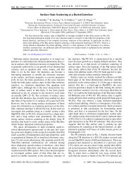
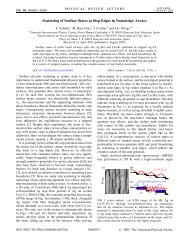
of fundamental issues, e.g. a proper description of Fig. 1: Schematic diagram of an “ideal” organic<br />
diode with two tunnel contacts [3].<br />
phenomena (e.g. charge injection) occurring at the<br />
electrode/OSC interface. Unfortunately, there are pronounced problems with growing highly<br />
ordered OSC-films on (strictly clean) metal substrate [1]. An attractive alternative to produce<br />
well-defined interfaces also suited for a theoretical analysis is to modify the metal electrode by<br />
adsorbing a well-defined thiolate-based self-assembled monolayer (SAM) [2]. This approach not<br />
only allows adjusting the work-function of the metal, but also provides structurally perfect<br />
substrates well suited for the OMBD-process.<br />
In this talk we will demonstrate that on an Au substrate covered with a decanethiolate SAM,<br />
pentacene, one of the most interesting molecules to be used as organic semiconductor in OFETs, can<br />
be grown in a rather perfect, bulk-like structure. The high structural quality and the absence of any<br />
contaminations make it possible to produce a two-terminal organoelectronic model device as shown<br />
in Fig. 1 [3]. This “ideal” device is essentially free of imperfections and well suited for a theoretical<br />
analysis. The results of numeric simulations [3] reveal that, at positive bias, n-transport dominates<br />
p-transport, an unusual behavior for pentacene-based devices.<br />
The n-conduction within the OSC pentacene can be suppressed by introducing OH-groups at the<br />
SAM/OSC interface, a finding which is in accord with related experiments on OFETs [4]. Recent<br />
experiments indicate that loading of the OH-traps with electrons is a reversible process [5].<br />
Fabrication of functioning OFET devices confirms the positive effect of SAM surface modification<br />
on device properties [6].<br />
A recent investigation of nanographene-based SAMs has demonstrated that using the<br />
SAM-approach relative molecular orientations can be achieved which are different from that present<br />
in the corresponding bulk phases, with very positive effects on the charge carrier mobilities [7].<br />
References<br />
[1] G.Witte and Ch.Wöll, J.Mater.Res. 19, 1889 (2004)<br />
[2] M. Kind and C. Wöll, Prog. Surf. Sci. 84, 230 (2009)<br />
[3] L.Ruppel, A.Birkner, G.Witte, C.Busse, T.Lindner, G.Paasch, C.Wöll, J.Appl.Phys. 102,<br />
033708 (2007)<br />
[4] L.Chua, J.Zaumseil, J.Chang, E.Ou, P.Ho, H.Sirringhaus, R.Friend, Nature 434, 194 (2005)<br />
[5] Z.-H. Wang, D. Käfer, A. Bashir, J. Götzen, A. Birkner, G. Witte, Ch. Wöll,<br />
PhysChemChemPhys, 12, 4317-4323 (2010)<br />
[6] C.Bock, D.Pham, U.Kunze, D.Käfer, G.Witte, Ch.Wöll, J.Appl.Phys. 100, 114517 (2006)<br />
[7] D. Käfer, A. Bashir, X. Dou, G. Witte, K. Müllen, Ch. Wöll, Adv. Mater, 22, 384-388 (2010)<br />
39