Strains and stresses in GaN heteroepitaxy â sources and ... - Laytec
Strains and stresses in GaN heteroepitaxy â sources and ... - Laytec
Strains and stresses in GaN heteroepitaxy â sources and ... - Laytec
SHOW LESS

Create successful ePaper yourself
Turn your PDF publications into a flip-book with our unique Google optimized e-Paper software.
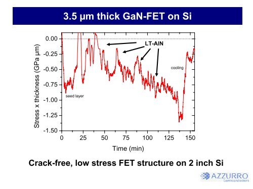
Stress x thickness (GPa µm)<br />
0.00<br />
-0.25<br />
-0.50<br />
-0.75<br />
-1.00<br />
-1.25<br />
-1.50<br />
3.5 µm thick <strong>GaN</strong>-FET on Si<br />
seed layer<br />
cool<strong>in</strong>g<br />
0 25 50 75 100 125 150<br />
Time (m<strong>in</strong>)<br />
LT-AlN<br />
Crack-free, low stress FET structure on 2 <strong>in</strong>ch Si