Combined use of in-situ curvature and full- wafer ... - Laytec
Combined use of in-situ curvature and full- wafer ... - Laytec
Combined use of in-situ curvature and full- wafer ... - Laytec

Create successful ePaper yourself
Turn your PDF publications into a flip-book with our unique Google optimized e-Paper software.
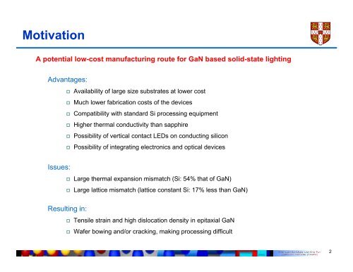
Motivation<br />
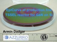
A potential low-cost manufactur<strong>in</strong>g route for GaN based solid-state light<strong>in</strong>g<br />
Advantages:<br />
Issues:<br />
� Availability <strong>of</strong> large size substrates at lower cost<br />
� Much lower fabrication costs <strong>of</strong> the devices<br />
� Compatibility with st<strong>and</strong>ard Si process<strong>in</strong>g equipment<br />
� Higher thermal conductivity than sapphire<br />
� Possibility <strong>of</strong> vertical contact LEDs on conduct<strong>in</strong>g silicon<br />
� Possibility <strong>of</strong> <strong>in</strong>tegrat<strong>in</strong>g electronics <strong>and</strong> optical devices<br />
� Large thermal expansion mismatch (Si: 54% that <strong>of</strong> GaN)<br />
� Large lattice mismatch (lattice constant Si: 17% less than GaN)<br />
Result<strong>in</strong>g <strong>in</strong>:<br />
� Tensile stra<strong>in</strong> <strong>and</strong> high dislocation density <strong>in</strong> epitaxial GaN<br />
� Wafer bow<strong>in</strong>g <strong>and</strong>/or crack<strong>in</strong>g, mak<strong>in</strong>g process<strong>in</strong>g difficult<br />
2