

ADuM3190 (Rev. 0) - Analog Devices
ADuM3190 (Rev. 0) - Analog Devices
ADuM3190 (Rev. 0) - Analog Devices

Create successful ePaper yourself
Turn your PDF publications into a flip-book with our unique Google optimized e-Paper software.
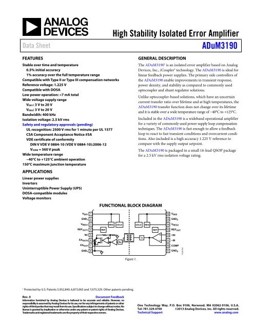
High Stability Isolated Error Amplifier<br />
Data Sheet <strong>ADuM3190</strong><br />
FEATURES<br />
Stable over time and temperature<br />
0.5% initial accuracy<br />
1% accuracy over the full temperature range<br />
Compatible with Type II or Type III compensation networks<br />
Reference voltage: 1.225 V<br />
Compatible with DOSA<br />
Low power operation:
<strong>ADuM3190</strong> Data Sheet<br />
TABLE OF CONTENTS<br />
Features .............................................................................................. 1<br />
Applications ....................................................................................... 1<br />
General Description ......................................................................... 1<br />
Functional Block Diagram .............................................................. 1<br />
<strong>Rev</strong>ision History ............................................................................... 2<br />
Specifications ..................................................................................... 3<br />
Package Characteristics ............................................................... 4<br />
Regulatory Information ............................................................... 4<br />
Insulation and Safety Related Specifications ............................ 4<br />
Recommended Operating Conditions ...................................... 4<br />
DIN V VDE V 0884-10 (VDE V 0884-10) Insulation<br />
Characteristics .............................................................................. 5<br />
Absolute Maximum Ratings ....................................................... 6<br />
ESD Caution .................................................................................. 6<br />
REVISION HISTORY<br />
2/13—<strong>Rev</strong>ision 0: Initial Version<br />
<strong>Rev</strong>. 0 | Page 2 of 16<br />
Pin Configuration and Function Descriptions ..............................7<br />
Typical Performance Characteristics ..............................................8<br />
Test Circuits ..................................................................................... 11<br />
Applications Information .............................................................. 12<br />
Theory of Operation .................................................................. 12<br />
Accuracy Circuit Operation...................................................... 12<br />
Application Block Diagram ...................................................... 12<br />
Setting the Output Voltage ........................................................ 13<br />
DOSA Module Application ....................................................... 14<br />
DC Correctness and Magnetic Field Immunity .......................... 14<br />
Insulation Lifetime ..................................................................... 15<br />
Packaging and Ordering Information ......................................... 16<br />
Outline Dimensions ................................................................... 16<br />
Ordering Guide .......................................................................... 16
Data Sheet <strong>ADuM3190</strong><br />
SPECIFICATIONS<br />
VDD1 = VDD2 = 3 V to 20 V for TA = TMIN to TMAX. All typical specifications are at TA = 25°C and VDD1 = VDD2 = 5 V, unless otherwise noted.<br />
Table 1.<br />
Parameter Test Conditions/Comments Min Typ Max Unit<br />
ACCURACY (1.225 V − EAOUT)/1.225 V × 100%; see Figure 18<br />
Initial Error TA = 25°C 0.25 0.5 %<br />
Total Error<br />
OP AMP<br />
TA = TMIN to TMAX 0.5 1 %<br />
Offset Error −5 ±2.5 +5 mV<br />
Open-Loop Gain 66 80 dB<br />
Input Common-Mode Range 0.35 1.5 V<br />
Gain Bandwidth Product 10 MHz<br />
Common-Mode Rejection 72 dB<br />
Input Capacitance 2 pF<br />
Output Voltage Range COMP pin 0.2 2.7 V<br />
Input Bias Current<br />
REFERENCE<br />
0.01 μA<br />
Output Voltage At 25°C, 0 mA to 1 mA load, CREFOUT = 15 pF 1.215 1.225 1.235 V<br />
−40°C to +125°C, 0 mA to 1 mA load, CREFOUT = 15 pF 1.213 1.225 1.237 V<br />
Output Current<br />
UVLO<br />
CREFOUT = 15 pF 2.0 mA<br />
Positive Going Threshold 2.8 2.96 V<br />
Negative Going Threshold 2.4 2.6 V<br />
EAOUT Impedance<br />
OUTPUT CHARACTERISTICS<br />
VDD2 < UVLO threshold or VDD1 < UVLO threshold High-Z Ω<br />
Output Gain From COMP to EAOUT, dc, 0.3 V to 2.4 V; and from<br />
COMP to EAOUT2, dc, 0.4 V to 5.0 V<br />
0.9 1.0 1.1 V/V<br />
Output −3 dB Bandwidth<br />
From COMP to EAOUT, 0.3 V to 2.4 V, ±3 mA; and from<br />
COMP to EAOUT2, 0.4 V to 5.0 V, ±1 mA<br />
2.34 2.6 2.86 V/V<br />
A and S Grades 100 200 kHz<br />
B and T Grades<br />
Output Voltage<br />
250 400 kHz<br />
EAOUT ±3 mA output<br />
Low 0.4 V<br />
High 2.4 2.5 V<br />
EAOUT2 ±1 mA output<br />
Low VDD1 = 4.5 V to 5.5 V 0.3 0.6 V<br />
High VDD1 = 4.5 V to 5.5 V 4.8 4.9 V<br />
Low VDD1 = 10 V to 20 V 0.3 0.6 V<br />
High VDD1 = 10 V to 20 V 5.0 5.4 V<br />
Noise See Figure 18<br />
EAOUT 1.7 mV rms<br />
EAOUT2<br />
POWER SUPPLY<br />
4.8 mV rms<br />
Operating Range, Side 1 VDD1 3.0 20 V<br />
Operating Range, Side 2 VDD2 3.0 20 V<br />
Power Supply Rejection<br />
Supply Current<br />
DC, VDD1 = VDD2 = 3 V to 20 V 60 dB<br />
IDD1 See Figure 18 1.4 2.0 mA<br />
IDD2 See Figure 18 2.9 5.0 mA<br />
<strong>Rev</strong>. 0 | Page 3 of 16
<strong>ADuM3190</strong> Data Sheet<br />
PACKAGE CHARACTERISTICS<br />
Table 2.<br />
Parameter<br />
RESISTANCE<br />
Symbol Min Typ Max Unit Test Conditions/Comments<br />
Input-to-Output1 RI-O 1013 CAPACITANCE<br />
Ω<br />
Input-to-Output1 CI-O 2.2 pF f = 1 MHz<br />
Input Capacitance 2 CI 4.0 pF<br />
IC JUNCTION-TO-AMBIENT THERMAL<br />
RESISTANCE<br />
Thermocouple located at center of package underside<br />
16-Lead QSOP θJA 76 °C/W<br />
1 The device is considered a 2-terminal device; Pin 1 through Pin 8 are shorted together, and Pin 9 through Pin 16 are shorted together.<br />
2 Input capacitance is from any input data pin to ground.<br />
REGULATORY INFORMATION<br />
The <strong>ADuM3190</strong> is pending approval by the organizations listed in Table 3. See Table 8 and the Insulation Lifetime section for<br />
recommended maximum working voltages for specific cross-isolation waveforms and insulation levels.<br />
Table 3.<br />
UL (Pending) CSA (Pending) VDE (Pending)<br />
Recognized Under 1577 Component<br />
Recognition Program1 Approved under CSA Component<br />
Certified according to DIN V VDE V 0884-10<br />
Acceptance Notice #5A<br />
(VDE V 0884-10): 2006-122 Single Protection, 2500 V rms Isolation<br />
Voltage, 16-Lead QSOP<br />
Basic insulation per CSA 60950-1-03 and<br />
IEC 60950-1, 400 V rms (565 V peak)<br />
maximum working voltage<br />
<strong>Rev</strong>. 0 | Page 4 of 16<br />
Reinforced insulation, 560 V peak<br />
File E214400 File 205078 File 2471900-4880-0001<br />
1 In accordance with UL 1577, each <strong>ADuM3190</strong> is proof tested by applying an insulation test voltage ≥ 3000 V rms for 1 sec (current leakage detection limit = 5 µA).<br />
2 In accordance with DIN V VDE V 0884-10, each <strong>ADuM3190</strong> is proof tested by applying an insulation test voltage ≥ 1050 V peak for 1 sec (partial discharge detection<br />
limit = 5 pC). The asterisk (*) marked on the component designates DIN V VDE V 0884-10 approval.<br />
INSULATION AND SAFETY RELATED SPECIFICATIONS<br />
Table 4.<br />
Parameter Symbol Value Unit Test Conditions/Comments<br />
Rated Dielectric Insulation Voltage 2500 V rms 1-minute duration<br />
Minimum External Air Gap (Clearance) L(I01) 3.8 min mm Measured from input terminals to output terminals,<br />
shortest distance through air<br />
Minimum External Tracking (Creepage) L(I02) 3.1 min mm Measured from input terminals to output terminals,<br />
shortest distance path along body<br />
Minimum Internal Gap (Internal Clearance) 0.017 min mm Insulation distance through insulation<br />
Tracking Resistance (Comparative Tracking Index) CTI >400 V DIN IEC 112/VDE 0303, Part 1<br />
Isolation Group II Material Group DIN VDE 0110, 1/89, Table 1<br />
RECOMMENDED OPERATING CONDITIONS<br />
Table 5.<br />
Parameter Symbol Min Max Unit<br />
OPERATING TEMPERATURE BY MODEL TA<br />
<strong>ADuM3190</strong>A/<strong>ADuM3190</strong>B −40 +85 °C<br />
<strong>ADuM3190</strong>S/<strong>ADuM3190</strong>T −40 +125 °C<br />
SUPPLY VOLTAGES 1 VDD1, VDD2 3.0 20 V<br />
INPUT SIGNAL RISE AND FALL TIMES tR, tF 1.0 ms<br />
1 All voltages are relative to their respective grounds.
Data Sheet <strong>ADuM3190</strong><br />
DIN V VDE V 0884-10 (VDE V 0884-10) INSULATION CHARACTERISTICS<br />
These isolators are suitable for reinforced isolation only within the safety limit data. Maintenance of the safety data is ensured by<br />
protective circuits. The asterisk (*) marking branded on the package denotes DIN V VDE V 0884-10 approval for a 560 V peak working<br />
voltage.<br />
Table 6.<br />
Description<br />
Installation Classification per DIN VDE 0110<br />
Test Conditions/Comments Symbol Characteristic Unit<br />
For Rated Mains Voltage ≤ 150 V rms I to IV<br />
For Rated Mains Voltage ≤ 300 V rms I to III<br />
For Rated Mains Voltage ≤ 400 V rms I to II<br />
Climatic Classification 40/105/21<br />
Pollution Degree per DIN VDE 0110, Table 1 2<br />
Maximum Working Insulation Voltage VIORM 560 V peak<br />
Input-to-Output Test Voltage, Method B1<br />
Input-to-Output Test Voltage, Method A<br />
VIORM × 1.875 = Vpd(m), 100% production test,<br />
tini = tm = 1 sec, partial discharge < 5 pC<br />
Vpd(m) 1050 V peak<br />
After Environmental Tests Subgroup 1 VIORM × 1.5 = Vpd(m), tini = 60 sec,<br />
tm = 10 sec, partial discharge < 5 pC<br />
Vpd(m) 840 V peak<br />
After Input and/or Safety Test Subgroup 2 VIORM × 1.2 = Vpd(m), tini = 60 sec,<br />
Vpd(m) 672 V peak<br />
and Subgroup 3<br />
tm = 10 sec, partial discharge < 5 pC<br />
Highest Allowable Overvoltage VIOTM 3500 V peak<br />
Surge Isolation Voltage VPEAK = 10 kV; 1.2 µs rise time; 50 µs, 50% fall time VIOSM 4000 V peak<br />
Safety Limiting Values Maximum value allowed in the event of a failure<br />
(see Figure 2)<br />
Case Temperature TS 150 °C<br />
Safety Total Dissipated Power PS 1.64 W<br />
Insulation Resistance at TS VIO = 500 V RS >109 Ω<br />
SAFE LIMITING POWER (W)<br />
1.8<br />
1.6<br />
1.4<br />
1.2<br />
1.0<br />
0.8<br />
0.6<br />
0.4<br />
0.2<br />
0<br />
0 50 100 150 200<br />
AMBIENT TEMPERATURE (°C) 11335-004<br />
Figure 2. Thermal Derating Curve, Dependence of Safety Limiting Values on Case<br />
Temperature, per DIN V VDE V 0884-10<br />
<strong>Rev</strong>. 0 | Page 5 of 16
<strong>ADuM3190</strong> Data Sheet<br />
ABSOLUTE MAXIMUM RATINGS<br />
TA = 25°C, unless otherwise noted.<br />
Table 7.<br />
Parameter Rating<br />
Storage Temperature (TST) Range −65°C to +150°C<br />
Ambient Operating Temperature<br />
(TA) Range<br />
−40°C to +125°C<br />
Junction Temperature<br />
Supply Voltages<br />
−40°C to +150°C<br />
VDD1, VDD2 1 −0.5 V to +24 V<br />
VREG1, VREG2 1 −0.5 V to +3.6 V<br />
Input Voltages (+IN, −IN)<br />
Output Voltages<br />
−0.5 V to +3.6 V<br />
REFOUT, COMP, REFOUT1, EAOUT −0.5 V to +3.6 V<br />
EAOUT2 −0.5 V to +5.5 V<br />
Output Current per Output Pin −11 mA to +11 mA<br />
Common-Mode Transients2 −100 kV/μs to +100 kV/μs<br />
1 All voltages are relative to their respective grounds.<br />
2 Refers to common-mode transients across the insulation barrier. Commonmode<br />
transients exceeding the absolute maximum ratings may cause<br />
latch-up or permanent damage.<br />
<strong>Rev</strong>. 0 | Page 6 of 16<br />
Stresses above those listed under Absolute Maximum Ratings<br />
may cause permanent damage to the device. This is a stress<br />
rating only; functional operation of the device at these or any<br />
other conditions above those indicated in the operational<br />
section of this specification is not implied. Exposure to absolute<br />
maximum rating conditions for extended periods may affect<br />
device reliability.<br />
Table 8. Maximum Continuous Working Voltage 1<br />
Parameter Max Unit Constraint<br />
WAVEFORM<br />
AC Voltage<br />
Bipolar 560 V peak 50-year minimum lifetime<br />
Unipolar 1131 V peak 50-year minimum lifetime<br />
DC Voltage 1131 V peak 50-year minimum lifetime<br />
1 Refers to continuous voltage magnitude imposed across the isolation<br />
barrier. See the Insulation Lifetime section for more details.<br />
ESD CAUTION
Data Sheet <strong>ADuM3190</strong><br />
PIN CONFIGURATION AND FUNCTION DESCRIPTIONS<br />
VDD1 1<br />
2<br />
VREG1 3<br />
REFOUT1 4<br />
NC 5<br />
EAOUT2 6<br />
EAOUT 7<br />
GND1 8<br />
<strong>ADuM3190</strong><br />
TOP VIEW<br />
(Not to Scale)<br />
Figure 3. Pin Configuration<br />
Table 9. Pin Function Descriptions<br />
Pin No. Mnemonic Description<br />
1 VDD1 Supply Voltage for Side 1 (3.0 V to 20 V). Connect a 1 μF capacitor between VDD1 and GND1.<br />
2 GND1 Ground Reference for Side 1.<br />
3 VREG1 Internal Supply Voltage for Side 1. Connect a 1 μF capacitor between VREG1 and GND1.<br />
4 REFOUT1 Reference Output Voltage for Side 1. The maximum capacitance for this pin (CREFOUT1) must not exceed 15 pF.<br />
5 NC No Connection. Connect Pin 5 to GND1; do not leave this pin floating.<br />
6 EAOUT2 Isolated Output Voltage 2, Open-Drain Output. Connect a pull-up resistor between EAOUT2 and VDD1 for current up to<br />
1 mA.<br />
7 EAOUT Isolated Output Voltage.<br />
8 GND1 Ground Reference for Side 1.<br />
9 GND2 Ground Reference for Side 2.<br />
10 COMP Output of the Op Amp. A loop compensation network can be connected between the COMP pin and the −IN pin.<br />
11 −IN Inverting Op Amp Input. Pin 11 is the connection for the power supply setpoint and compensation network.<br />
12 +IN Noninverting Op Amp Input. Pin 12 can be used as a reference input.<br />
13 REFOUT Reference Output Voltage for Side 2. The maximum capacitance for this pin (CREFOUT) must not exceed 15 pF.<br />
14 VREG2 Internal Supply Voltage for Side 2. Connect a 1 μF capacitor between VREG2 and GND2.<br />
15 GND2 Ground Reference for Side 2.<br />
16 VDD2 Supply Voltage for Side 2 (3.0 V to 20 V). Connect a 1 μF capacitor between VDD2 and GND2.<br />
<strong>Rev</strong>. 0 | Page 7 of 16<br />
16 VDD2 15 GND2 14 VREG2 13 REFOUT 12 +IN<br />
11 –IN<br />
10 COMP<br />
9 GND2 NC = NO CONNECTION. CONNECT PIN 5 TO GND 1 ;<br />
DO NOT LEAVE THIS PIN FLOATING.<br />
11335-005
<strong>ADuM3190</strong> Data Sheet<br />
TYPICAL PERFORMANCE CHARACTERISTICS<br />
I DD1 (mA)<br />
I DD2 (mA)<br />
INPUT BIAS CURRENT (nA)<br />
3<br />
2<br />
1<br />
0<br />
–40 –20 0 20 40 60 80 100 120 140<br />
5<br />
4<br />
3<br />
2<br />
1<br />
V DDx = 20V<br />
V DDx = 5V<br />
TEMPERATURE (°C)<br />
Figure 4. Typical IDD1 Supply Current vs. Temperature<br />
0<br />
–40 –20 0 20 40 60 80 100 120 140<br />
12<br />
10<br />
8<br />
6<br />
4<br />
2<br />
V DDx = 20V<br />
V DDx = 5V<br />
TEMPERATURE (°C)<br />
Figure 5. Typical IDD2 Supply Current vs. Temperature<br />
0<br />
–40 –20 0 20 40 60 80 100 120 140<br />
TEMPERATURE (°C) 11335-019<br />
Figure 6. +IN, −IN Input Bias Current vs. Temperature<br />
11335-017<br />
11335-018<br />
REF OUT ACCURACY (V)<br />
<strong>Rev</strong>. 0 | Page 8 of 16<br />
1.228<br />
1.227<br />
1.226<br />
1.225<br />
1.224<br />
1.223<br />
1.222<br />
–40 –20 0 20 40 60 80 100 120 140<br />
TEMPERATURE (°C) 11335-020<br />
EA OUT ACCURACY (%)<br />
1.0<br />
0.5<br />
0<br />
–0.5<br />
Figure 7. REFOUT Accuracy vs. Temperature<br />
–1.0<br />
–40 –20 0 20 40 60 80 100 120 140<br />
TEMPERATURE (°C) 11335-021<br />
OP AMP OFFSET VOLTAGE (mV)<br />
3<br />
2<br />
1<br />
0<br />
–1<br />
–2<br />
Figure 8. EAOUT Accuracy vs. Temperature<br />
–3<br />
–40 –20 0 20 40 60 80 100 120 140<br />
TEMPERATURE (°C) 11335-022<br />
Figure 9. Op Amp Offset Voltage vs. Temperature
Data Sheet <strong>ADuM3190</strong><br />
OP AMP OPEN-LOOP GAIN (dB)<br />
EA OUT GAIN (V/V)<br />
EA OUT2 GAIN (V/V)<br />
100<br />
90<br />
80<br />
70<br />
60<br />
50<br />
–40 –20<br />
1.05<br />
1.04<br />
1.03<br />
1.02<br />
1.01<br />
0 20 40 60 80 100 120 140<br />
TEMPERATURE (°C)<br />
Figure 10. Op Amp Open-Loop Gain vs. Temperature<br />
1.00<br />
–40 –20<br />
2.70<br />
2.68<br />
2.66<br />
2.64<br />
2.62<br />
2.60<br />
–40 –20<br />
0 20 40 60 80 100 120 140<br />
TEMPERATURE (°C)<br />
Figure 11. EAOUT Gain vs. Temperature<br />
0 20 40 60 80 100 120 140<br />
TEMPERATURE (°C)<br />
Figure 12. EAOUT2 Gain vs. Temperature<br />
11335-023<br />
11335-024<br />
11335-025<br />
EA OUT OFFSET (mV)<br />
EA OUT2 OFFSET (mV)<br />
<strong>Rev</strong>. 0 | Page 9 of 16<br />
0<br />
–20<br />
–40<br />
–60<br />
–80<br />
–100<br />
–40 –20<br />
0<br />
–50<br />
–100<br />
–150<br />
–200<br />
–250<br />
–300<br />
–40 –20<br />
1<br />
2<br />
0 20 40 60 80 100 120 140<br />
TEMPERATURE (°C)<br />
Figure 13. EAOUT Offset vs. Temperature<br />
0 20 40 60 80 100 120 140<br />
TEMPERATURE (°C)<br />
Figure 14. EAOUT2 Offset vs. Temperature<br />
CH1 10mV Ω CH2 10mV Ω M4.0µs<br />
T 102.4ns<br />
A CH1 1.18V<br />
Figure 15. Output Noise with Test Circuit 1, Channel 1 = EAOUT (10 mV/div),<br />
Channel 2 = EAOUT2 (10 mV/div)<br />
11335-028<br />
11335-026<br />
11335-027
<strong>ADuM3190</strong> Data Sheet<br />
1<br />
2<br />
3<br />
CH1 100mV Ω CH2 100mV Ω M2µs A CH1 434mV<br />
CH3 200mV Ω<br />
T 0s<br />
Figure 16. Output 100 kHz Signal with Test Circuit 3, Channel 1 = +IN,<br />
Channel 2 = EAOUT, Channel 3 = EAOUT2<br />
11335-029<br />
<strong>Rev</strong>. 0 | Page 10 of 16<br />
2<br />
1<br />
3<br />
CH1 20mV Ω CH2 50mV Ω M2µs A CH1 399mV<br />
CH3 20mV Ω<br />
T 5.92µs<br />
Figure 17. Output Square Wave Response with Test Circuit 3,<br />
Channel 1 = +IN, Channel 2 = EAOUT, Channel 3 = EAOUT2<br />
11335-030
Data Sheet <strong>ADuM3190</strong><br />
TEST CIRCUITS<br />
1µF<br />
1µF<br />
1µF<br />
1µF<br />
V DD1<br />
GND1 VREG1 GND 1<br />
1<br />
2<br />
3<br />
REFOUT1 4<br />
NC 5<br />
EAOUT2 6<br />
EAOUT 7<br />
8<br />
1<br />
2<br />
3<br />
REFOUT1 4<br />
ROD NC 5<br />
EAOUT2 6<br />
EAOUT 7<br />
1µF<br />
1µF<br />
R OD<br />
VDD1 GND1 VREG1 GND 1<br />
8<br />
V DD1<br />
GND 1<br />
V REG1<br />
REF OUT1<br />
NC<br />
EA OUT2<br />
EA OUT<br />
GND 1<br />
1<br />
2<br />
3<br />
4<br />
5<br />
6<br />
7<br />
8<br />
REF<br />
REF<br />
REF<br />
REG UVLO UVLO<br />
Rx<br />
Tx<br />
Figure 18. Test Circuit 1<br />
REG UVLO UVLO<br />
Rx<br />
Tx<br />
Figure 19. Test Circuit 2<br />
REG UVLO UVLO<br />
Rx<br />
Figure 20. Test Circuit 3<br />
<strong>Rev</strong>. 0 | Page 11 of 16<br />
REG<br />
REG<br />
Tx<br />
REF<br />
REG<br />
REF<br />
REF<br />
VDD2 16<br />
GND2 15<br />
1µF<br />
VREG2 14<br />
1µF<br />
13 REFOUT 12 +IN<br />
–IN 680Ω<br />
11<br />
COMP 2.2nF<br />
10<br />
9<br />
GND 2<br />
VDD2 16<br />
GND2 15<br />
1µF<br />
VREG2 14<br />
1µF<br />
13 REFOUT 12 +IN<br />
–IN<br />
680Ω<br />
11<br />
COMP<br />
2.2nF<br />
10<br />
9<br />
GND 2<br />
VDD2 16<br />
GND2 15<br />
VREG2 14<br />
13 REFOUT +IN<br />
12<br />
–IN<br />
11<br />
COMP<br />
10<br />
9<br />
GND 2<br />
1µF<br />
1µF<br />
11335-002<br />
11335-031<br />
11335-003
<strong>ADuM3190</strong> Data Sheet<br />
APPLICATIONS INFORMATION<br />
THEORY OF OPERATION<br />
In the test circuits of the <strong>ADuM3190</strong> (see Figure 18 through<br />
Figure 20), external supply voltages from 3 V to 20 V are<br />
provided to the VDD1 and VDD2 pins, and internal regulators<br />
provide 3.0 V to operate the internal circuits of each side of the<br />
<strong>ADuM3190</strong>. An internal precision 1.225 V reference provides<br />
the reference for the ±1% accuracy of the isolated error amplifier.<br />
UVLO circuits monitor the VDDx supplies to turn on the internal<br />
circuits when the 2.8 V rising threshold is met and to turn off<br />
the error amplifier outputs to a high impedance state when VDDx<br />
falls below 2.6 V.<br />
approximately 100 kHz, but the circuit is more stable with a phase<br />
shift of approximately −120°, which yields a stable 60° phase<br />
margin.<br />
This circuit is used for accuracy tests only, not for real-world<br />
applications, because it has a 680 Ω resistor across the isolation<br />
barrier to close the loop for the error amplifier; this resistor<br />
causes leakage current to flow across the isolation barrier. For<br />
this test circuit only, GND1 must be connected to GND2 to create a<br />
return for the leakage current created by the 680 Ω resistor<br />
connection.<br />
AMPLITUDE (dB)<br />
The op amp on the right side of the device has a noninverting<br />
100<br />
OP AMP AND<br />
+IN pin and an inverting −IN pin available for connecting a<br />
LINEAR ISOLATOR<br />
feedback voltage in an isolated dc-to-dc converter output, usually<br />
through a voltage divider. The COMP pin is the op amp output,<br />
which can be used to attach resistor and capacitor components in<br />
LINEAR ISOLATOR<br />
POLE AT 400kHz<br />
100 1k 10k 100k 1M<br />
OP AMP<br />
ALONE<br />
FREQUENCY<br />
10M (Hz)<br />
a compensation network. The COMP pin internally drives the Tx<br />
LINEAR<br />
transmitter block, which converts the op amp output voltage<br />
PHASE (°)<br />
ISOLATOR<br />
into an encoded output that is used to drive the digital isolator<br />
transformer.<br />
–90<br />
100 1k 10k 100k 1M 10M FREQUENCY<br />
(Hz)<br />
On the left side of the <strong>ADuM3190</strong>, the transformer output<br />
PWM signal is decoded by the Rx block, which converts the<br />
signal into a voltage that drives an amplifier block; the amplifier<br />
–180<br />
block produces the error amplifier output available at the EAOUT<br />
Figure 21. Bode Plot 1<br />
pin. The EAOUT pin can deliver ±3 mA and has a voltage level<br />
AMPLITUDE (dB)<br />
between 0.4 V and 2.4 V, which is typically used to drive the<br />
input of a PWM controller in a dc-to-dc circuit.<br />
100<br />
OP AMP AND<br />
LINEAR ISOLATOR<br />
LINEAR ISOLATOR<br />
For applications that need more output voltage to drive their<br />
controllers, Figure 19 illustrates the use of the EAOUT2 pin output<br />
which delivers up to ±1 mA with an output voltage of 0.6 V to 4.8 V<br />
for an output that has a pull-up resistor to a 5 V supply. If the<br />
INTEGRATOR<br />
CONFIGURATION<br />
100 1k 10k 100k<br />
POLE AT 400kHz<br />
OP AMP<br />
ALONE<br />
FREQUENCY<br />
1M 10M (Hz)<br />
EAOUT2 pull-up resistor connects to a 10 V to 20 V supply, the<br />
PHASE (°)<br />
output is specified to a minimum of 5.0 V to allow use with a<br />
PWM controller requiring a minimum input operation of 5 V.<br />
–90<br />
100 1k 10k 100k 1M 10M FREQUENCY<br />
(Hz)<br />
ACCURACY CIRCUIT OPERATION<br />
See Figure 18 and Figure 19 for stability of the accuracy circuits.<br />
–180<br />
The op amp on the right side of the <strong>ADuM3190</strong>, from the −IN<br />
pin to the COMP pin, has a unity-gain bandwidth (UGBW) of<br />
Figure 22. Bode Plot 2<br />
10 MHz. Figure 21, Bode Plot 1, shows a dashed line for the op<br />
APPLICATION BLOCK DIAGRAM<br />
amp alone and its 10 MHz pole.<br />
Figure 23 shows a typical application, an isolated error amplifier<br />
Figure 21 also shows the linear isolator alone (the blocks from<br />
in primary side control, for the <strong>ADuM3190</strong>. The op amp of the<br />
the op amp output to the <strong>ADuM3190</strong> output, labeled as the<br />
<strong>ADuM3190</strong> is used as the error amplifier for the feedback of the<br />
linear isolator), which introduces a pole at approximately<br />
output voltage, VOUT, using a resistor divider to the −IN pin of<br />
400 kHz. This total Bode plot of the op amp and linear isolator<br />
the op amp. This configuration inverts the output signal at the<br />
shows that the phase shift is approximately −180° from the −IN<br />
COMP pin when compared to the +IN pin, which is connected<br />
pin to the EAOUT pin before the crossover frequency. Because a<br />
to the internal 1.225 V reference. For example, when the output<br />
−180° phase shift can make the system unstable, adding an inte-<br />
voltage, VOUT, falls due to a load step, the divider voltage at the<br />
grator configuration, as shown in the test circuits in Figure 18 and −IN pin falls below the +IN reference voltage, causing the COMP<br />
Figure 19, consisting of a 2.2 nF capacitor and a 680 Ω resistor,<br />
pin output signal to go high. The COMP output of the op amp<br />
helps to make the system stable. In Figure 22, Bode Plot 2 with an is encoded and then decoded back by the digital isolator trans-<br />
integrator configuration added, the system crosses over 0 dB at<br />
former block to a signal that drives the output of the <strong>ADuM3190</strong><br />
<strong>Rev</strong>. 0 | Page 12 of 16<br />
11335-006<br />
11335-007
Data Sheet <strong>ADuM3190</strong><br />
high. The output of the <strong>ADuM3190</strong> drives the COMP pin of<br />
the PWM controller, which is designed to reset the PWM latch<br />
output to low only when its COMP pin is low. A high at the<br />
COMP pin has the effect of making the latching PWM comparator<br />
produce a PWM duty cycle output. This PWM duty<br />
cycle output drives the power stage to increase the VOUT voltage<br />
until it returns to regulation.<br />
PWM CONTROLLER<br />
V REF<br />
FB COMP<br />
EA OUT2<br />
ERROR<br />
AMP<br />
OSC<br />
LATCHING<br />
PWM<br />
CURRENT<br />
SENSE<br />
COMP<br />
<strong>ADuM3190</strong><br />
POWER<br />
STAGE<br />
1.225V<br />
–IN<br />
+IN<br />
REF OUT<br />
Figure 23. Application Block Diagram 1<br />
The power stage output is filtered by output capacitance and, in<br />
some applications, by an inductor. Various elements contribute<br />
to the gain and phase of the control loop and the resulting stability.<br />
The Output Filter L and Output Filter C components create a<br />
double pole; the op amp has a pole at 10 MHz (see Figure 21),<br />
and the linear isolator has a pole at 400 kHz (see Figure 21 and<br />
Figure 22).<br />
The output capacitor and its ESR can add a zero at a frequency<br />
that is dependent on the component type and values. With the<br />
<strong>ADuM3190</strong> providing the error amplifier, a compensation<br />
network is provided from the −IN pin to the COMP pin to<br />
compensate the control loop for stability. The compensation<br />
network values depend on both the application and the components<br />
that are selected; information about the component<br />
network values is provided in the data sheet of the selected<br />
PWM controller.<br />
The <strong>ADuM3190</strong> has two different error amplifier outputs,<br />
EAOUT and EAOUT2. The EAOUT output, which can drive ±3 mA,<br />
has a guaranteed maximum high output voltage of at least 2.4 V,<br />
which may not be enough to drive the COMP pin of some PWM<br />
controllers. The EAOUT2 pin can drive ±1 mA and has an output<br />
range that guarantees 5.0 V for a VDD1 voltage range of 10 V to<br />
20 V, which works well with the COMP pin of many PWM<br />
controllers.<br />
In an application where the 5 V minimum output of the EAOUT2<br />
pin is not enough to drive the COMP pin of some PWM controllers,<br />
for example, controllers that operate with 6 V or more<br />
of COMP pin voltage, use EAOUT2 to drive the FB pin of the error<br />
amplifier of the PWM controller (see Figure 24). The typical VREF<br />
voltage level of PWM controllers is approximately 1.25 V or<br />
2.5 V, setting the reference level for the FB pin. In Figure 24, the<br />
V IN<br />
L O<br />
DCR<br />
C O<br />
ESR<br />
C COMPENSATION<br />
1<br />
NETWORK<br />
C2 R2 OP AMP<br />
+<br />
V OUT<br />
11335-008<br />
<strong>Rev</strong>. 0 | Page 13 of 16<br />
EAOUT2 output is used for a PWM controller with a 2.5 V<br />
reference.<br />
PWM CONTROLLER<br />
OSC<br />
VREF ERROR<br />
AMP LATCHING<br />
PWM<br />
FB COMP<br />
EA OUT2<br />
CURRENT<br />
SENSE<br />
POWER<br />
STAGE<br />
COMP<br />
OP AMP<br />
1.225V<br />
–IN<br />
+IN<br />
REF OUT<br />
Figure 24. Application Block Diagram 2<br />
As shown in Figure 24, the <strong>ADuM3190</strong> op amp has the feedback<br />
voltage from the VOUT output divider is connected to the<br />
+IN pin, and the +1.225 V reference voltage connected to the<br />
−IN pin. This configuration produces a low going <strong>ADuM3190</strong><br />
COMP pin when the VOUT voltage drops from a load step. The<br />
EAOUT2 pin follows the COMP pin, going low and connecting to<br />
the PWM controller FB pin. The error amplifier of the PWM<br />
controller has a reference (VREF) at the noninverting input,<br />
which, when the FB pin is low, makes the COMP pin of the<br />
error amplifier output go high. A high at the COMP pin causes<br />
the latching PWM comparator to produce a PWM duty cycle<br />
output. This PWM duty cycle output drives the power stage to<br />
increase the VOUT voltage until it returns to regulation.<br />
The application block diagrams (see Figure 23 and Figure 24)<br />
show two different ways to use the <strong>ADuM3190</strong> to provide isolated<br />
feedback in the control loop of an isolated dc-to-dc converter.<br />
In both figures, the loop is closed at approximately the 1.225 V<br />
reference voltage, providing ±1% accuracy over temperature. The<br />
<strong>ADuM3190</strong> op amp has a high gain bandwidth of 10 MHz to<br />
allow the dc-to-dc converter to operate at high switching speeds,<br />
enabling smaller values for the Output Filter L and Output Filter C<br />
components.<br />
The 400 kHz bandwidth of the <strong>ADuM3190</strong> error amplifier output<br />
offers faster loop response for better transient response than the<br />
typical shunt regulator and optocoupler solutions, which typically<br />
have bandwidths of only 25 kHz to 50 kHz maximum.<br />
SETTING THE OUTPUT VOLTAGE<br />
The output voltage in the application circuit can be set with two<br />
resistors in a voltage divider, as shown in Figure 25.<br />
The output voltage is determined by the following equation,<br />
where VREF = 1.225 V:<br />
VOUT = VREF × (R1 + R2)/R2 (1)<br />
V IN<br />
C1 COMPENSATION<br />
C2 R2<br />
NETWORK<br />
<strong>ADuM3190</strong><br />
L O<br />
DCR<br />
C O<br />
ESR<br />
+<br />
V OUT<br />
11335-009
<strong>ADuM3190</strong> Data Sheet<br />
Figure 25. Setting the Output Voltage<br />
DOSA MODULE APPLICATION<br />
Figure 26 is a block diagram of a Distributed-power Open<br />
Standards Alliance (DOSA) circuit using the <strong>ADuM3190</strong>. The<br />
block diagram shows how to use the <strong>ADuM3190</strong> 1.225 V reference<br />
and the error amp in a DOSA standard power supply module<br />
circuit to produce output voltage settings using a combination<br />
of resistors.<br />
The <strong>ADuM3190</strong> 1.225 V reference is specified for ±1% over the<br />
−40°C to +125°C temperature range. See Table 10 to select the<br />
resistor values to set the output voltage of the module. Two<br />
different ranges of VOUT can be implemented, VOUT > 1.5 V or<br />
VOUT < 1.5 V, depending on the required module.<br />
ERROR<br />
AMP<br />
ERROR<br />
AMP<br />
<strong>ADuM3190</strong><br />
ISOLATED DC-TO-DC SUPPLY<br />
<strong>ADuM3190</strong><br />
DOSA MODULE<br />
V IN = 0.35V TO 1.5V<br />
V REF<br />
1.225V<br />
V IN = 0.35V TO 1.5V<br />
V REF<br />
1.225V<br />
R 5<br />
Figure 26. DOSA Module<br />
Table 10. Resistor Values for DOSA Module<br />
Module<br />
Nominal Output R3 R4 R5 R6<br />
VOUT > 1.5 V 1 kΩ 1 kΩ 0 Ω Open<br />
VOUT < 1.5 V 1 kΩ 0 Ω 2.05 kΩ 1.96 kΩ<br />
VOUT > 1.5 V 5.11 kΩ 5.11 kΩ 0 Ω Open<br />
VOUT < 1.5 V 5.11 kΩ 0 Ω 10.5 kΩ 10.0 kΩ<br />
DC CORRECTNESS AND MAGNETIC FIELD IMMUNITY<br />
Positive and negative logic transitions at the isolator input cause<br />
narrow (~1 ns) pulses to be sent to the decoder via the transformer.<br />
The decoder is bistable and is, therefore, either set or reset by<br />
the pulses, indicating input logic transitions. In the absence of<br />
logic transitions of more than 1 µs at the input, a periodic set of<br />
refresh pulses indicative of the correct input state are sent to<br />
ensure dc correctness at the output.<br />
If the decoder receives no internal pulses for more than approximately<br />
3 µs, the input side is assumed to be unpowered or<br />
nonfunctional, in which case, the isolator output is forced to<br />
R 1<br />
R 2<br />
R 4<br />
R 6<br />
R 3<br />
–IN<br />
+IN<br />
REF OUT<br />
V OUT<br />
R 1<br />
R 2<br />
R TRIM-UP<br />
V OUT<br />
R TRIM-DOWN<br />
11335-010<br />
OPTIONAL TRIM-UP<br />
OR TRIM-DOWN<br />
RESISTOR OR ±10%<br />
OF NOMINAL VALUE<br />
ACCORDING TO DOSA<br />
11335-011<br />
<strong>Rev</strong>. 0 | Page 14 of 16<br />
a default high impedance state by the watchdog timer circuit. In<br />
addition, the outputs are in a default high impedance state while<br />
the power is increasing before the UVLO threshold is crossed.<br />
The <strong>ADuM3190</strong> is immune to external magnetic fields. The limitation<br />
on the <strong>ADuM3190</strong> magnetic field immunity is set by the<br />
condition whereby induced voltage in the transformer receiving<br />
coil is sufficiently large to either falsely set or reset the decoder.<br />
The following analysis defines the conditions under which this<br />
can occur. The 3 V operating condition of the <strong>ADuM3190</strong> is<br />
examined because it represents the most susceptible mode of<br />
operation. The pulses at the transformer output have an amplitude<br />
that is greater than 1.0 V. The decoder has a sensing threshold at<br />
approximately 0.5 V, therefore establishing a 0.5 V margin within<br />
which induced voltages are tolerated. The voltage induced across<br />
the receiving coil is given by<br />
V = (−dβ/dt) ∑π rn 2 , n = 1, 2, … , N<br />
where:<br />
β is the magnetic flux density (gauss).<br />
rn is the radius of the nth turn in the receiving coil (cm).<br />
N is the number of turns in the receiving coil.<br />
Given the geometry of the receiving coil in the <strong>ADuM3190</strong> and<br />
an imposed requirement that the induced voltage be, at most,<br />
50% of the 0.5 V margin at the decoder, a maximum allowable<br />
magnetic field is calculated, as shown in Figure 27.<br />
MAXIMUM ALLOWABLE MAGNETIC FLUX<br />
DENSITY (kgauss)<br />
100<br />
10<br />
1<br />
0.1<br />
0.01<br />
0.001<br />
1k 10k 100k 1M 10M<br />
MAGNETIC FIELD FREQUENCY (Hz)<br />
Figure 27. Maximum Allowable External Magnetic Flux Density<br />
100M<br />
For example, at a magnetic field frequency of 1 MHz, the maximum<br />
allowable magnetic field of 0.02 kgauss induces a voltage<br />
of 0.25 V at the receiving coil. This is approximately 50% of the<br />
sensing threshold and does not cause a faulty output transition.<br />
Similarly, if such an event were to occur during a transmitted<br />
pulse (and had the worst-case polarity), the received pulse is<br />
reduced from >1.0 V to 0.75 V, still well above the 0.5 V sensing<br />
threshold of the decoder.<br />
The preceding magnetic flux density values correspond to<br />
specific current magnitudes at given distances away from the<br />
<strong>ADuM3190</strong> transformers. Figure 28 shows these allowable<br />
current magnitudes as a function of frequency for selected distances.<br />
As shown Figure 28, the <strong>ADuM3190</strong> is immune and can<br />
11335-012
Data Sheet <strong>ADuM3190</strong><br />
be affected only by extremely large currents operating at a high<br />
frequency very close to the component. For the 1 MHz example,<br />
a 0.7 kA current must be placed 5 mm away from the <strong>ADuM3190</strong><br />
to affect the operation of the device.<br />
100<br />
10<br />
1<br />
0.1<br />
MAXIMUM ALLOWABLE CURRENT (kA) 1000<br />
DISTANCE = 100mm<br />
DISTANCE = 5mm<br />
0.01<br />
1k 10k 100k 1M 10M 100M<br />
MAGNETIC FIELD FREQUENCY (Hz)<br />
Figure 28. Maximum Allowable Current for Various<br />
Current-to-<strong>ADuM3190</strong> Spacings<br />
INSULATION LIFETIME<br />
DISTANCE = 1m<br />
All insulation structures eventually break down when subjected<br />
to voltage stress over a sufficiently long period. The rate of insulation<br />
degradation is dependent on the characteristics of the<br />
voltage waveform applied across the insulation. In addition<br />
to the testing performed by the regulatory agencies, <strong>Analog</strong><br />
<strong>Devices</strong> carries out an extensive set of evaluations to determine<br />
the lifetime of the insulation structure within the <strong>ADuM3190</strong>.<br />
<strong>Analog</strong> <strong>Devices</strong> performs accelerated life testing using voltage<br />
levels higher than the rated continuous working voltage. Acceleration<br />
factors for several operating conditions are determined.<br />
These factors allow calculation of the time to failure at the actual<br />
working voltage.<br />
The values shown in Table 8 summarize the peak voltage for<br />
50 years of service life for a bipolar ac operating condition. In<br />
many cases, the approved working voltage is higher than the<br />
50-year service life voltage. Operation at these high working<br />
voltages can lead to shortened insulation life in some cases.<br />
11335-013<br />
<strong>Rev</strong>. 0 | Page 15 of 16<br />
The <strong>ADuM3190</strong> insulation lifetime depends on the voltage waveform<br />
type imposed across the isolation barrier. The iCoupler<br />
insulation structure degrades at different rates depending on<br />
whether the waveform is bipolar ac, unipolar ac, or dc. Figure 29,<br />
Figure 30, and Figure 31 illustrate these different isolation<br />
voltage waveforms.<br />
A bipolar ac voltage environment is the worst case for the iCoupler<br />
products yet meets the 50-year operating lifetime recommended<br />
by <strong>Analog</strong> <strong>Devices</strong> for maximum working voltage. In the case<br />
of unipolar ac or dc voltage, the stress on the insulation is significantly<br />
lower. This allows operation at higher working voltages<br />
while still achieving a 50-year service life. Treat any cross-insulation<br />
voltage waveform that does not conform to Figure 30 or Figure 31<br />
as a bipolar ac waveform, and limit its peak voltage to the 50-year<br />
lifetime voltage value listed in Table 8.<br />
Note that the voltage presented in Figure 30 is shown as sinusoidal<br />
for illustration purposes only. It is meant to represent any<br />
voltage waveform varying between 0 V and some limiting value.<br />
The limiting value can be positive or negative, but the voltage<br />
cannot cross 0 V.<br />
RATED PEAK VOLTAGE<br />
0V<br />
Figure 29. Bipolar AC Waveform<br />
RATED PEAK VOLTAGE<br />
0V<br />
Figure 30. Unipolar AC Waveform<br />
RATED PEAK VOLTAGE<br />
0V<br />
Figure 31. DC Waveform<br />
11335-014<br />
11335-015<br />
11335-016
<strong>ADuM3190</strong> Data Sheet<br />
PACKAGING AND ORDERING INFORMATION<br />
OUTLINE DIMENSIONS<br />
Figure 32. 16-Lead Shrink Small Outline Package [QSOP]<br />
(RQ-16)<br />
Dimensions shown in inches and (millimeters)<br />
ORDERING GUIDE<br />
Model1 Temperature Range Bandwidth (Typical) Package Description<br />
Package<br />
Option<br />
<strong>ADuM3190</strong>ARQZ −40°C to +85°C 200 kHz 16-Lead QSOP RQ-16<br />
<strong>ADuM3190</strong>ARQZ-RL7 −40°C to +85°C 200 kHz 16-Lead QSOP RQ-16<br />
<strong>ADuM3190</strong>BRQZ −40°C to +85°C 400 kHz 16-Lead QSOP RQ-16<br />
<strong>ADuM3190</strong>BRQZ-RL7 −40°C to +85°C 400 kHz 16-Lead QSOP RQ-16<br />
<strong>ADuM3190</strong>SRQZ −40°C to +125°C 200 kHz 16-Lead QSOP RQ-16<br />
<strong>ADuM3190</strong>SRQZ-RL7 −40°C to +125°C 200 kHz 16-Lead QSOP RQ-16<br />
<strong>ADuM3190</strong>TRQZ −40°C to +125°C 400 kHz 16-Lead QSOP RQ-16<br />
<strong>ADuM3190</strong>TRQZ-RL7 −40°C to +125°C 400 kHz 16-Lead QSOP RQ-16<br />
EVAL-<strong>ADuM3190</strong>EBZ Evaluation Board<br />
1 Z = RoHS Compliant Part.<br />
0.065 (1.65)<br />
0.049 (1.25)<br />
0.010 (0.25)<br />
0.004 (0.10)<br />
COPLANARITY<br />
0.004 (0.10)<br />
16 9<br />
1<br />
0.025 (0.64)<br />
BSC<br />
0.197 (5.00)<br />
0.193 (4.90)<br />
0.189 (4.80)<br />
©2013 <strong>Analog</strong> <strong>Devices</strong>, Inc. All rights reserved. Trademarks and<br />
registered trademarks are the property of their respective owners.<br />
D11335-0-2/13(0)<br />
8<br />
0.012 (0.30)<br />
0.008 (0.20)<br />
0.158 (4.01)<br />
0.154 (3.91)<br />
0.150 (3.81)<br />
0.069 (1.75)<br />
0.053 (1.35)<br />
SEATING<br />
PLANE<br />
0.244 (6.20)<br />
0.236 (5.99)<br />
0.228 (5.79)<br />
COMPLIANT TO JEDEC STANDARDS MO-137-AB<br />
CONTROLLING DIMENSIONS ARE IN INCHES; MILLIMETER DIMENSIONS<br />
(IN PARENTHESES) ARE ROUNDED-OFF INCH EQUIVALENTS FOR<br />
REFERENCE ONLY AND ARE NOT APPROPRIATE FOR USE IN DESIGN.<br />
<strong>Rev</strong>. 0 | Page 16 of 16<br />
8°<br />
0°<br />
0.010 (0.25)<br />
0.006 (0.15)<br />
0.050 (1.27)<br />
0.016 (0.41)<br />
0.020 (0.51)<br />
0.010 (0.25)<br />
0.041 (1.04)<br />
REF<br />
01-28-2008-A<br />
www.analog.com/<strong>ADuM3190</strong>


