
Create successful ePaper yourself
Turn your PDF publications into a flip-book with our unique Google optimized e-Paper software.
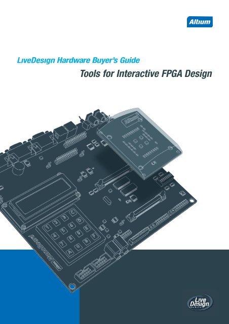
Hardware Buyer’s Guide<br />
Tools for Interactive FPGA Design
Making electronics design easier <br />
<strong>Altium</strong> has always been at the forefront of desktop EDA technology.<br />
<strong>Altium</strong> defined the future of desktop design with the release of the<br />
world’s first Windows ® -based PCB design tool. Our latest 2004 product<br />
line continues this history of innovation by bringing to the engineer’s<br />
desktop a complete electronics design system that covers board-level,<br />
system-on-FPGA and complete embedded system design technologies.<br />
<strong>Altium</strong> creates design solutions that bring together the best of<br />
electronic design and contemporary software technology to keep<br />
pace with the changing nature of today’s and tomorrow’s electronics<br />
design processes. <strong>Altium</strong>’s edge lies in making its products affordable<br />
and easy to use for all designers whilst putting the very best<br />
technology into all of its products.<br />
Our philosophy is a simple one – we want every designer in the<br />
world to have access to the best possible design tools at an affordable<br />
price and to make the engineer’s desktop the most powerful,<br />
productive and cost-effective design platform.<br />
At <strong>Altium</strong> we truly believe in making electronics design easier.<br />
So let us make life easier for you...<br />
“<br />
The philosophy behind <strong>Altium</strong>’s vision is a belief that<br />
all designers must have easy access to the best available<br />
electronic design tools, and that these tools must be easy<br />
to use and truly affordable. This is essential if we are<br />
to continue to see great innovation.”<br />
Nick Martin<br />
Founder and Joint CEO – <strong>Altium</strong> Limited
LiveDesign Hardware Buyer’s Guide<br />
Tools for Interactive FPGA Design<br />
Section 01 Interactive FPGA design with the NanoBoard 4<br />
02 FPGA device support 8<br />
03 <strong>Device</strong> <strong>reference</strong> <strong>guide</strong> 14<br />
<strong>Altium</strong>’s unique reconfigurable development platform<br />
– the NanoBoard – allows rapid and interactive<br />
implementation and debugging of your FPGA design.<br />
Target programmable devices are housed on plug-in<br />
daughter boards, allowing you to easily change the<br />
target project architecture, providing a truly FPGA<br />
vendor-independent development solution.<br />
For flexible systems design, multiple NanoBoards can<br />
be chained together to support the development of<br />
complex systems comprising of multiple FPGA devices<br />
spread across multiple PCBs. Connections on the<br />
NanoBoard for user-developed boards enables easy<br />
porting of designs to your own dedicated PCB.<br />
The NanoBoard, in combination with <strong>Altium</strong>’s extensive<br />
range of LiveDesign-enabled development solutions,<br />
will transform your desktop into a complete and<br />
interactive FPGA-based electronics design laboratory.
SECTION 01 INTERACTIVE FPGA DESIGN NANOBOARD-NB1 2004<br />
4<br />
Why should I use<br />
<strong>Altium</strong>’s NanoBoard<br />
over other<br />
development boards?<br />
Fully LiveDesign enabled<br />
for seamless integration<br />
with <strong>Altium</strong>’s 2004 family<br />
of design tools<br />
Multiple target devices<br />
are included<br />
Vendor-independence is<br />
supported by having the<br />
reprogrammable device<br />
(FPGA, CPLD) on a<br />
daughter board; the<br />
target is changed by<br />
replacing one daughter<br />
board with another<br />
A complex system of<br />
NanoBoards running the<br />
same or different projects<br />
can be created by<br />
chaining several<br />
NanoBoards together<br />
Working with FPGAbased<br />
user boards only<br />
requires a JTAG<br />
connection since the<br />
NanoBoard acts to<br />
control the design<br />
download to the user<br />
board plus all interactions<br />
with processors and<br />
virtual instruments<br />
A rich set of peripherals<br />
and connectors are<br />
included on the board<br />
for design flexibility<br />
Interactive FPGA design with<br />
the NanoBoard <br />
The NanoBoard is a unique, sophisticated, device- and vendorindependent<br />
FPGA-based development board that allows rapid<br />
and interactive implementation and debugging of FPGA designs.<br />
<strong>Altium</strong>’s new NanoBoard (nano-level breadboard)<br />
is the industry’s first FPGA-based, LiveDesign-enabled<br />
development board. The NanoBoard allows rapid<br />
and interactive implementation and debugging<br />
of FPGA designs and has been specially designed<br />
to take full advantage of <strong>Altium</strong>’s 2004 family of<br />
LiveDesign-enabled design tools. Target programmable<br />
devices are housed on plug-in daughter boards,<br />
enabling engineers to easily change the target<br />
project architecture, providing a truly FPGA<br />
vendor-independent development board.<br />
For flexible systems design, multiple NanoBoards can<br />
be chained together to support the development of<br />
complex systems comprising of multiple FPGA devices<br />
spread across multiple PCBs. Connections on the<br />
NanoBoard for user-developed boards enables easy<br />
porting of designs to your own dedicated PCB, which<br />
can be linked into the system via the NanoBoard to<br />
extend the LiveDesign process to the production PCB.<br />
As well as providing communications to and from<br />
the FPGA, the NanoBoard incorporates a wide range<br />
of peripherals such as an LCD, RAM, serial flash<br />
memory, keypad and ADC/DAC that can easily<br />
be used for application development. Ports on the<br />
NanoBoard include PS2, RS232, CAN, VGA, and I2C,<br />
as well as a range of general purpose I/O headers.<br />
The NanoBoard, in combination with <strong>Altium</strong>’s<br />
extensive range of LiveDesign-enabled electronics<br />
development tools, will transform your desktop into<br />
a complete and interactive FPGA-based electronics<br />
design laboratory.<br />
FPGA vendor and target independent<br />
The NanoBoard features swappable daughter boards<br />
that house the target programmable device. This<br />
allows easy reconfiguration of the NanoBoard to<br />
support multiple device families from different FPGA<br />
vendors. <strong>Altium</strong>’s LiveDesign-enabled design systems,<br />
such as Protel ®<br />
and Nexar , take full advantage<br />
of this by offering a device-independent design<br />
environment that allows a single design to be<br />
retargeted to a wide range of programmable<br />
devices, providing true design portability.<br />
Cyclone <br />
Plug-in daughter boards with Altera ®<br />
(EP1C12-Q240C7) and Xilinx ®<br />
Spartan ®<br />
(XC2S300E-<br />
PQ208) FPGAs are supplied as standard with<br />
the NanoBoard.<br />
Change the target FPGA easily by swapping daughter boards.<br />
The system will automatically recognise the installed device.<br />
NanoBoard-NB1 2004 – LiveDesign-enabled FPGA-based development board www.altium.com/nanoboard
Build a complex system by daisy chaining multiple NanoBoards.<br />
Chaining of multiple NanoBoards<br />
The NanoBoard includes both Master and Slave<br />
NanoTalk connectors that allow multiple NanoBoards<br />
to be chained together when used with <strong>Altium</strong>’s<br />
LiveDesign-enabled design systems. The NanoTalk<br />
controller manages the routing of signals between<br />
the boards to maintain continuity of the JTAG<br />
chains across NanoBoards. The target device on<br />
each NanoBoard forms a hard JTAG chain that is<br />
accessible via the system software. Similarly, all<br />
devices (such as Nexus processor cores and virtual<br />
instruments contained within the designs) running<br />
on each of the NanoBoards form a continuous ‘soft’<br />
chain that is also accessible via the design software.<br />
The system software allows you to target different<br />
FPGA projects to each NanoBoard in the chain,<br />
allowing you to develop complex systems that<br />
contain multiple FPGAs that may be implemented<br />
over several PCBs.<br />
Connect your production board to the design system via the NanoBoard and<br />
continue the LiveDesign process on the final PCB.<br />
Connection of production PCBs<br />
The NanoBoard includes connectors for the<br />
integration of a designer’s production PCB into the<br />
LiveDesign environment. By exposing the hard and<br />
soft JTAG chains in your design, you can connect<br />
your production PCB to the NanoBoard via a 10-way<br />
header. The JTAG devices on your board will appear<br />
in the LiveDesign-enabled design environment as<br />
devices on the hard JTAG chain. Soft devices such<br />
as Nexus process cores and virtual instruments<br />
running on the FPGAs on your production board<br />
will appear in the soft chain and are accessible<br />
through the design environment. This extends the<br />
LiveDesign process to the design and debugging of<br />
your production board. Up to two user boards can<br />
be connected to each NanoBoard in the system.<br />
Features overview<br />
The NanoBoard is fully<br />
compatible with all <strong>Altium</strong><br />
DXP 2004-based systems<br />
FPGA vendor and device<br />
independent<br />
Plug-in daughter board<br />
system supports a wide<br />
range of target FPGAs<br />
Altera ® Cyclone (EP1C12-<br />
Q240C7) daughter board<br />
supplied<br />
Xilinx ® Spartan ® IIE<br />
(XC2S300E-PQ208)<br />
daughter board supplied<br />
Other device daughter boards<br />
can be purchased separately<br />
System automatically detects<br />
installed FPGA device<br />
Multiple NanoBoards<br />
can be chained together –<br />
NanoBoard controller<br />
manages routing of hard<br />
and soft JTAG chains<br />
Up to two user boards can be<br />
connected to the NanoBoard<br />
with automatic routing of<br />
hard and soft JTAG chains<br />
Includes power pack<br />
with multiple plugs for<br />
various electrical outlet<br />
configurations<br />
Includes ribbon cable for PC<br />
connection plus other cables<br />
and connectors<br />
Extensive NanoBoard<br />
technical hardware<br />
<strong>reference</strong> manual<br />
Peripherals include: LCD,<br />
LED array, switch array,<br />
keypad, buzzer, ADC/DAC,<br />
256K x 8 RAM, 8M serial flash<br />
RAM, on-board serial flash<br />
RAM for FPGA config,<br />
programmable clock<br />
Ports include: PS2 mouse<br />
and keyboard, RS232, CAN,<br />
VGA, I2C, general purpose<br />
I/O headers<br />
continued overleaf<br />
SECTION 01 INTERACTIVE FPGA DESIGN NANOBOARD-NB1 2004<br />
5
SECTION 01 INTERACTIVE FPGA DESIGN NANOBOARD NANOBOARD-NB1 NB1 2004<br />
6<br />
TDI<br />
U2<br />
LAX_1K16<br />
Running<br />
Logic<br />
Analyser<br />
TDI TDO<br />
Interactive hardware<br />
debug<br />
Debugging circuitry inside<br />
an FPGA can be a difficult<br />
task. Internal signals can<br />
be brought out to the pins<br />
of the FPGA for monitoring<br />
and testing, but this adds<br />
to the complexity of the<br />
design process. What’s<br />
needed is a way to<br />
examine and control<br />
signals inside the FPGA.<br />
The DXP 2004 system<br />
provides a library of virtual<br />
instruments that can be<br />
wired into your circuit at<br />
the schematic level. The<br />
instruments comprise a<br />
hardware portion that is<br />
synthesized and downloaded<br />
into the target FPGA, and<br />
a soft instrument panel<br />
controllable from the PC.<br />
Instruments communicate<br />
with the system via a<br />
secondary ‘soft’ JTAG chain<br />
that is established inside<br />
the FPGA and brought<br />
out to defined pins on the<br />
NanoBoard. These virtual<br />
instruments then give<br />
you a window into the<br />
operation of the loaded<br />
FPGA for interactive<br />
debugging of your design.<br />
What ‘breadboarding at the nano level’<br />
has to offer<br />
1 RS232<br />
The DTE RS232 connector provides TXD, RXD, RTS<br />
and CTS signal lines connected to the target FPGA<br />
via level translation circuitry.<br />
2 CAN<br />
The CAN connector is interfaced to the target<br />
FPGA via a CAN protocol transceiver with<br />
configurable speed.<br />
3 VGA<br />
NB1 includes a VGA-compatible RGB video monitor<br />
port. The port is configured with two bits per color,<br />
a total of six bits per pixel or 64 colors. The port is<br />
directly connected to I/O pins on the target FPGA.<br />
4 NanoTalk configuration header<br />
Uses jumpers to configure the operational mode<br />
of the NB1 NanoTalk controller and to set the<br />
default clock rate.<br />
5 PS2<br />
Two standard PS2 ports are available on NB1<br />
and are directly connected to I/O pins on the<br />
target FPGA. These are nominally intended for<br />
the connection of a PC keyboard and mouse<br />
to the FPGA design.<br />
6 Parallel port connection to PC<br />
NB1 connects to a PC via a standard parallel port. A<br />
cable for this purpose is supplied with the NanoBoard.<br />
7 Power connectors<br />
Two parallel power connector jacks are provided<br />
so that power can be supplied to a chain of<br />
NanoBoards in daisychain configuration.<br />
8 NanoTalk Slave<br />
Multiple NanoBoards can be chained together using<br />
the NanoTalk Master and NanoTalk Slave headers.<br />
Connectors are provided for this. The NanoBoard<br />
controllers manage the routing of JTAG chains<br />
between boards to provide access to all hard and<br />
soft devices on all chained boards.<br />
9 NanoBoard controller<br />
The NB1 controller performs a variety of tasks,<br />
including managing the routing of the various<br />
JTAG chains to and from the target devices and<br />
controlling communications to and from the design<br />
software running on the PC. The controller is<br />
implemented inside a reconfigurable FPGA device<br />
to allow for firmware upgrades in the field.<br />
10 Serial flash RAM<br />
NB1 includes two 8Mbit serial flash RAM resources.<br />
These can be programmed by the design system via<br />
the NanoBoard controller. One of the devices can be<br />
set as a source to configure the target FPGA on<br />
power up.<br />
11 Daughter board sockets<br />
Dual high-cycle sockets are used to plug in the<br />
swappable daughter boards containing target FPGA<br />
devices. The daughter boards allow the NanoBoard<br />
to be used with a variety of programmable devices.<br />
12 Static RAM<br />
NB1 provides two 128k x 8 static RAM devices, which<br />
are directly connected to I/O pins on the target FPGA<br />
device. The SRAM devices have a common Chip Select<br />
and address lines, but separate 8-bit data bus and<br />
RD/RW signals for each chip. The memory resource<br />
can be application-configured as single 128k x 16 or<br />
256k x 8 address space, or two 128k x 8 spaces.<br />
13 Programmable system clock<br />
SPI-based programmable clock generator that<br />
provides a fixed 20MHz <strong>reference</strong> clock and userprogrammed<br />
clock with an output frequency from<br />
6 to 200MHz. Both clocks are connected to global<br />
clock pins on the plug-in target FPGA.<br />
14 DIP switch<br />
8-way DIP switch, accessible directly from target FPGA.<br />
15 LED array<br />
8 x high intensity LED array, accessible directly from<br />
target FPGA.<br />
16 Test/reset button<br />
General purpose momentary-action pushbutton,<br />
accessed directly from the target FPGA. This has no<br />
intrinsically set function, but is nominally intended<br />
to be used as a hard reset button for the FPGAbased<br />
circuit.<br />
17 General purpose headers<br />
A total of 36 target FPGA I/O lines are terminated<br />
on the two general purpose User Headers on NB1.<br />
These headers also provide ground and power.<br />
18 ADC/DAC & I2C<br />
NB1 is equipped with general purpose analog<br />
to digital and digital to analog converters, both<br />
interfaced using the I2C protocol. Four channels<br />
are provided as well as a filtered 3.3V analog<br />
supply and ground. The same signals are<br />
available via a header, which additionally provides<br />
I2C signals and a 5V supply and power ground.<br />
NanoBoard-NB1 2004 – LiveDesign-enabled FPGA-based development board www.altium.com/nanoboard
23<br />
22<br />
21<br />
The <strong>Altium</strong> NanoBoard is the first<br />
LiveDesign-enabled development<br />
platform for Nexar and Protel<br />
19 Audio CODEC<br />
NB1 provides an 8-bit audio CODEC, together with<br />
relevant analog pre- and post- conditioning circuitry,<br />
terminated with stereo input and output jacks.<br />
The CODEC is accessible from the target FPGA.<br />
20 User board connectors<br />
NB1 includes two user board JTAG headers.<br />
These headers are used to include a user-developed<br />
board in the hard and soft JTAG chains, and can<br />
be used to extend the LiveDesign process to your<br />
production PCB.<br />
21 Keypad<br />
1 2 3 4 5 6 7<br />
20<br />
A 16-way keypad is provided for user input to the<br />
FPGA circuit. The keypad is arranged in a 4 x 4 array<br />
and organized so that a row-column scanning<br />
19<br />
18<br />
24<br />
process can read the status of each key. The keypad<br />
features replaceable overlays.<br />
22 LCD<br />
NB1 includes a standard 16 character by two line<br />
LCD with LED backlight, accessible directly from<br />
the target FPGA.<br />
23 Buzzer<br />
17<br />
NB1 includes a magnetic audio transducer<br />
connected to an I/O line on the target FPGA.<br />
24 High capacity FPGA daughter boards<br />
Included as standard with the NanoBoard are<br />
the two most popular FPGA daughter boards to<br />
accommodate reconfigurable systems including<br />
processor-based designs.<br />
8<br />
9<br />
10<br />
11<br />
12<br />
13<br />
14<br />
15<br />
16<br />
Features overview<br />
On-board programmable<br />
clock (frequencies from<br />
6MHz to 200MHz, software<br />
controllable) and fixed<br />
frequency <strong>reference</strong> clock<br />
Upgradeable NanoBoard<br />
controller firmware<br />
Integrated heavy-duty<br />
NanoBoard stand<br />
DXP 2004 software<br />
support for NanoBoard<br />
Comprehensive set of FPGAbased<br />
virtual instruments for<br />
interactive hardware debug<br />
Virtual instruments include<br />
soft front panels that<br />
communicate with the design<br />
running on the NanoBoard<br />
Virtual instruments include<br />
logic analyzers, frequency<br />
counters, frequency<br />
generators, I/O blocks<br />
Central control of FPGA<br />
design processing and<br />
download<br />
<strong>Device</strong>s view allows<br />
interaction with all<br />
NanoBoards connected<br />
to the system, all FPGA<br />
target devices and all soft<br />
devices contained within<br />
the downloaded designs<br />
FPGA vendor tools<br />
(supplied separately) driven<br />
transparently through DXP<br />
interface for place and<br />
route<br />
NanoBoard port plug-in<br />
library allows convenient<br />
schematic-level connection<br />
to NanoBoard devices<br />
Configuration Manager<br />
allows FPGA project to<br />
be easily retargeted from<br />
NanoBoard to final PCB<br />
implementation<br />
SECTION 01 INTERACTIVE FPGA DESIGN NANOBOARD-NB1 2004<br />
7
SECTION 02 FPGA DEVICE SUPPORT NANOBOARD-NB1 2004<br />
8<br />
Hitting the target<br />
By providing target devices<br />
on plug-in daughter<br />
boards, <strong>Altium</strong> lowers the<br />
cost of development for<br />
companies that work with<br />
more than one device family.<br />
It also makes it easy to<br />
evaluate and compare the<br />
features and benefits of<br />
different devices without<br />
the need to support<br />
multiple development<br />
systems. Engineers can<br />
create their FPGA design<br />
and then plug-in different<br />
daughter boards to test the<br />
design on a wide variety of<br />
target FPGA architectures.<br />
The system also allows<br />
engineers to do design<br />
work on a device that is<br />
particularly suitable for<br />
development, and then<br />
switch to a different device<br />
for final production.<br />
FPGA device support<br />
Swappable FPGA daughter boards offer true device independence,<br />
allowing you to easily retarget your design to any device family and<br />
ensuring you always have access to the latest in FPGA device technology.<br />
With most development systems you’re limited<br />
to a single target device, and designing for<br />
different devices requires you to work on multiple<br />
development boards. <strong>Altium</strong>’s NanoBoard eliminates<br />
this constraint by housing the target device on a<br />
robust daughter board that plugs into the main<br />
board via a set of high-reliability connectors. This<br />
allows you to change the target device at any time,<br />
making it possible to develop systems for a range<br />
of device families from multiple FPGA vendors.<br />
System-wide device support<br />
The available range of daughter board devices<br />
is fully supported in the system software. When<br />
you swap daughter boards, the DXP 2004 system<br />
automatically recognizes the target device and<br />
configures the environment appropriately. In the<br />
<strong>Device</strong>s view the correct vendor tool set for place-<br />
&-route and timing analysis is automatically<br />
selected, and any project configurations valid<br />
for the target device are available for selection.<br />
<strong>Altium</strong>’s DXP 2004 product range comes with<br />
constraint files for each supported daughter board.<br />
These constraint files map the FPGA pinout on<br />
the daughter board to the relevant NanoBoard<br />
resources. You can add these constraint files to your<br />
project configuration to easily set up your project<br />
for download to the NanoBoard. Each project can<br />
have multiple configurations, allowing you to easily<br />
retarget your design for the full range of available<br />
daughter boards.<br />
<strong>Altium</strong>’s DXP 2004 product range comes with<br />
a range of FPGA-based components to allow<br />
for easy schematic-based system development.<br />
These components are supplied as a schematic<br />
symbol with attached FPGA models. All components<br />
are pre-synthesized and pre-verified to support all<br />
available target daughter boards. This means that<br />
your designs can be targeted to any supported<br />
device without the need to re-engineer the circuit.<br />
The correct models are automatically selected<br />
and instantiated based on the target device<br />
you have fitted.<br />
Continuously updated device support<br />
Manufacturers continually release new devices<br />
and device families. <strong>Altium</strong>’s development team<br />
is constantly adding additional device support and<br />
new daughter boards that can be dropped in to<br />
your existing system. This protects your design tool<br />
investment and allows you to expand your system<br />
as new devices come onto the market.<br />
With <strong>Altium</strong>’s NanoBoard and DXP 2004-based<br />
design systems your development environment<br />
is future-proof.<br />
The wide range of available daughter boards makes the NanoBoard<br />
a truly device and FPGA vendor-independent development platform.<br />
NanoBoard-NB1 2004 – LiveDesign-enabled FPGA-based development board www.altium.com/nanoboard
Available daughter boards<br />
FPGA <strong>Device</strong>s<br />
Actel ProASIC Plus <br />
<strong>Device</strong>: APA600-FPQ208<br />
The ProASIC Plus family of devices, Actel’s second generation Flash FPGAs, offers<br />
enhanced performance over Actel’s ProASIC family. It combines the advantages of<br />
ASICs with the benefits of programmable devices through nonvolatile Flash technology.<br />
This enables engineers to create high-density systems using existing ASIC or FPGA<br />
design flows and tools. In addition, the ProASIC Plus family offers a unique clock<br />
conditioning circuit based on two on-board phase-locked loops (PLLs). The family<br />
offers up to 1 million system gates, supported with up to 198kbits of 2-port SRAM<br />
and up to 712 user I/Os, all providing 50 MHz PCI performance.<br />
APA600 features:<br />
21,504 logic elements (as 3-input function generators), 600,000 system gates<br />
126 Kbits of embedded RAM (total)<br />
4 global clock networks<br />
2 phase-locked loops (PLLs) with flexible phase<br />
Support for 4 selectable I/O standards<br />
Altera ®<br />
Cyclone <br />
<strong>Device</strong>: EP1C12Q240C7<br />
The Cyclone field programmable gate array family is based on a 1.5-V, 0.13-µm,<br />
all-layer copper SRAM process, with densities up to 20,060 logic elements (LEs)<br />
and up to 288 Kbits of RAM.<br />
EP1C12 features:<br />
12,060 logic elements (as 4-input LUTs with programmable register<br />
and carry chain)<br />
239 Kbits of RAM (total)<br />
4 dedicated clocks and 8 dual-purpose clocks (DPCLK)<br />
2 phase-locked loops (PLLs)<br />
Support for 10 selectable I/O standards<br />
Altera ®<br />
Cyclone with SRAM<br />
<strong>Device</strong>: EP1C20F400C8<br />
The Cyclone field programmable gate array family is based on a 1.5-V, 0.13-µm,<br />
all-layer copper SRAM process, with densities up to 20,060 logic elements (LEs)<br />
and up to 288 Kbits of RAM.<br />
EP1C20 features:<br />
20,060 logic elements (as 4-input LUTs with programmable register<br />
and carry chain)<br />
294 Kbits of RAM (total)<br />
4 dedicated clocks, and 8 dual-purpose clocks (DPCLK)<br />
2 phase-locked loops (PLLs)<br />
Support for 10 selectable I/O standards<br />
Additional daughter board features:<br />
Two IDT71V416L static RAM ICs – 4 Meg (256K x 16) 10ns advanced<br />
high-speed CMOS<br />
SECTION 02 FPGA DEVICE SUPPORT NANOBOARD-NB1 2004<br />
9
SECTION 02 FPGA DEVICE SUPPORT NANOBOARD-NB1 2004<br />
10<br />
Altera ®<br />
Stratix with SRAM<br />
<strong>Device</strong>: EP1S10F780C7<br />
The Stratix family of FPGAs is based on a 1.5-V, 0.13-µm, all-layer copper<br />
SRAM process, with densities up to 79,040 logic elements (LEs) and up to<br />
7.5 Mbits of RAM.<br />
EP1S10 features:<br />
10,570 logic elements (as 4-input LUTs with programmable register<br />
and carry chain)<br />
920 Kbits RAM (total)<br />
6 digital signal processing (DSP) blocks<br />
24 embedded multipliers (18 x 18-bit)<br />
16 dedicated global clocks<br />
4 fast, and 2 enhanced phase-locked loops (PLLs)<br />
Support for 26 selectable I/O standards<br />
Additional daughter board features:<br />
Two IDT71V416L static RAM ICs – 4 Meg (256K x 16) 10ns advanced<br />
high-speed CMOS<br />
One MAX1617 SMBus temperature sensor which measures FPGA chip<br />
temperature and internal sensor temperature<br />
Xilinx ®<br />
Spartan ®<br />
-II<br />
<strong>Device</strong>: XC2S200-6PQ208C<br />
The Spartan ®<br />
-II 2.5V Field-Programmable Gate Array family gives users<br />
high performance, abundant logic resources, and a rich feature set, all at an<br />
exceptionally low price. The six-member family offers densities ranging from<br />
15,000 to 200,000 system gates. System performance is supported up to<br />
200 MHz.<br />
XC2S200 features:<br />
5,292 logic cells arranged in 2,352 CLB slices (200,000 system gates)<br />
Up to 4,704 4-input LUTs and 4,704 flip-flops<br />
Block RAM (to 56K bits) and distributed RAM (to 73.5K bits)<br />
4 digital clock managers (DLLs)<br />
4 primary low-skew global clock distribution nets<br />
Support for 16 selectable I/O standards<br />
Xilinx ®<br />
Spartan ®<br />
-IIE<br />
<strong>Device</strong>: XC2S300E-6PQ208C<br />
The Spartan ®<br />
-IIE 1.8V Field-Programmable Gate Array family gives users<br />
high performance, abundant logic resources, and a rich feature set, all at an<br />
exceptionally low price. The seven-member family offers densities ranging from<br />
50,000 to 600,000 system gates. System performance is supported beyond<br />
200 MHz.<br />
XC2S300E features:<br />
6,912 logic cells arranged in 3,072 CLB slices (300,000 system gates)<br />
Up to 6,144 4-input LUTs and 6,144 flip-flops<br />
Block RAM (to 64K bits) and distributed RAM (to 96K bits)<br />
4 digital clock managers (DLLs)<br />
4 primary low-skew global clock distribution nets<br />
Support for 19 selectable I/O standards with fast or slow slew rates<br />
and multiple drive strengths<br />
NanoBoard-NB1 2004 – LiveDesign-enabled FPGA-based development board www.altium.com/nanoboard
Xilinx ®<br />
Spartan ®<br />
-IIE with SRAM<br />
<strong>Device</strong>: XC2S600E-6FG456C<br />
The Spartan ®<br />
-IIE 1.8V Field-Programmable Gate Array family gives users<br />
high performance, abundant logic resources, and a rich feature set, all at an<br />
exceptionally low price. The seven-member family offers densities ranging from<br />
50,000 to 600,000 system gates. System performance is supported beyond<br />
200 MHz.<br />
XC2S600E features:<br />
15,552 logic cells arranged in 6,912 CLB slices (600,000 system gates)<br />
Up to 13,824 4-input LUTs and 13,824 flip-flops<br />
Block RAM (to 288K bits) and distributed RAM (to 216K bits)<br />
4 digital clock managers (DLLs)<br />
4 primary low-skew global clock distribution nets<br />
Support for 19 selectable I/O standards with fast or slow slew rates<br />
and multiple drive strengths<br />
Additional daughter board features:<br />
Two IDT71V416L static RAM ICs – 4 Meg (256K x 16) 10ns advanced high-speed CMOS<br />
Xilinx ®<br />
Spartan ®<br />
-3 with SRAM<br />
<strong>Device</strong>: XC3S1000-4FG456C<br />
The 1.2V Spartan ®<br />
-3 family of Field-Programmable Gate Arrays is specifically<br />
designed to meet the needs of high volume, cost-sensitive consumer electronic<br />
applications. The eight-member family offers densities ranging from 50,000<br />
to five million system gates.<br />
XC3S1000 features:<br />
17,280 logic cells arranged in 7,680 CLB slices (1000K system gates)<br />
Up to 15,360 4-input LUTs and 15,360 flip-flops<br />
Block RAM (to 432K bits) and distributed RAM (to 120K bits)<br />
4 digital clock managers (DLLs)<br />
8 global clock lines with abundant routing<br />
Support for 26 selectable I/O standards with fast or slow slew rates<br />
and multiple drive strengths<br />
Additional daughter board features:<br />
Two IDT71V416L static RAM ICs – 4 Meg (256K x 16) 10ns advanced high-speed CMOS<br />
Xilinx ®<br />
Virtex ®<br />
-II with SRAM<br />
<strong>Device</strong>: XC2V1000-4FG456C<br />
The Virtex ®<br />
-II family is a platform FPGA developed for high performance from<br />
low-density to high-density designs that are based on IP cores and customized<br />
modules. The family delivers complete solutions for telecommunication, wireless,<br />
networking, video, and DSP applications.<br />
XC2V1000 features:<br />
11,520 logic cells arranged in 5,120 CLB slices (1000K system gates)<br />
Up to 10,240 4-input LUTs and 10,240 flip-flops<br />
Block RAM (to 720K bits) and distributed RAM (to 160K bits)<br />
8 digital clock managers (DLLs)<br />
16 global clock multiplexer buffers<br />
Support for 34 selectable I/O standards with fast or slow slew rates<br />
and multiple drive strengths<br />
Additional daughter board features:<br />
Two IDT71V416L static RAM ICs – 4 Meg (256K x 16) 10ns advanced high-speed CMOS<br />
One MAX1617 SMBus temperature sensor which measures FPGA chip<br />
temperature and internal sensor temperature<br />
Optional key memory battery backup for bitstream encryption<br />
SECTION 02 FPGA DEVICE SUPPORT NANOBOARD-NB1 2004<br />
11
SECTION 02 FPGA DEVICE SUPPORT NANOBOARD-NB1 2004<br />
12<br />
CPLD <strong>Device</strong>s<br />
Xilinx ®<br />
Virtex-II Pro with SRAM<br />
<strong>Device</strong>: XC2VP7-5FG456C<br />
The Virtex ®<br />
-II Pro family contains platform FPGAs for designs that are based on<br />
IP cores and customized modules. The family incorporates multi-gigabit transceivers<br />
and PowerPC CPU blocks. It empowers complete solutions for telecommunication,<br />
wireless, networking, video, and DSP applications.<br />
XC2VP7 features:<br />
11,088 logic cells arranged in 4,928 CLB slices<br />
Up to 9,856 4-input LUTs and 9,856 flip-flops<br />
Block RAM (to 792K bits) and distributed RAM (to 154K bits)<br />
4 digital clock managers (DLLs)<br />
16 global clock multiplexer buffers<br />
Support for 32 selectable I/O standards with fast or slow slew rates<br />
and multiple drive strengths<br />
The device contains a ‘hard’ PowerPC 405 processor core, which is supported<br />
in Nexar by a complete tool-chain (TASKING Viper compiler, source level<br />
debugger, etc) that allows use of this device in FPGA-based system designs<br />
Additional daughter features:<br />
Two IDT71V416L static RAM ICs – 4 Meg (256K x 16) 10ns advanced<br />
high-speed CMOS<br />
One MAX1617 SMBus temperature sensor which measures FPGA chip<br />
temperature and internal sensor temperature<br />
Interface to two of the high speed (3.125GHz) transceivers in the Virtex-II Pro –<br />
each transceiver channel has 4 gold plated SMA coax connectors mounted along<br />
the top of the daughter board (transceivers are used with the programmable<br />
on-board Nanoboard clock that limits their speed to between 1 and 2GHz)<br />
The board comes with 8 coax connector cables and an example project that<br />
demonstrates the use of the transceivers<br />
Altera ®<br />
MAX ®<br />
3000/7000 with PLCC sockets<br />
<strong>Device</strong>: EPM7032AELC44-10<br />
The MAX ®<br />
family of devices are high-density, high performance devices based on<br />
Altera’s second-generation MAX architecture. The EEPROM-based devices operate<br />
with a 3.3-V supply voltage and provide 600 to 10,000 usable gates and counter<br />
speeds of up to 303.0 MHz, dependant on specific device.<br />
EPM7032AE features:<br />
32 macrocells<br />
2 dedicated global clocks<br />
3.3V supply voltage with 2.5 to 5V I/Os<br />
Support for 2 selectable I/O standards<br />
Additional daughter board features:<br />
The daughter board includes one 44 pin and one 84 pin PLCC socket providing<br />
support for any of the following devices: EPM3032A, EPM3064A, EPM7032S,<br />
EPM7064S, EPM7128S, EPM7160S, EPM7032AE, EPM7064AE, EPM7128AE,<br />
EPM7032B, EPM7064B, EPM7032S, EPM7064S, EPM7128S, EPM7160S.<br />
NanoBoard-NB1 2004 – LiveDesign-enabled FPGA-based development board www.altium.com/nanoboard
Xilinx ®<br />
CoolRunner ®<br />
-II<br />
<strong>Device</strong>: XC2C256-6PQ208C<br />
The Xilinx ®<br />
CoolRunner ®<br />
-II CPLDs deliver the high speed and ease of use associated<br />
with the XC9500/XL/XV CPLD family with the extremely low power versatility<br />
of the XPLA3 family in a single CPLD. Low power consumption and high-speed<br />
operation are combined into a single family that is easy to use and cost effective.<br />
XC2C256 features:<br />
256 macrocells<br />
2 separate I/O banks<br />
3 dedicated global clocks<br />
1.8V supply voltage with 1.5 to 3.3V I/Os<br />
Fast Zero Power (FZP) architecture<br />
Support for 8 selectable I/O standards<br />
Xilinx ®<br />
CoolRunner ®<br />
XPLA3<br />
<strong>Device</strong>: XCR3256XL-12PQ208C<br />
The CoolRunner ®<br />
XPLA3 (eXtended Programmable Logic Array) family of CPLDs<br />
is targeted for low power systems that include portable, handheld, and power<br />
sensitive applications. Each member of the XPLA3 family includes Fast Zero<br />
Power (FZP) design technology that combines low power and high speed.<br />
XCR3256XL features:<br />
256 macrocells<br />
4 dedicated global clocks<br />
3.3V supply voltage with 3.3 and 5V I/Os<br />
Fast Zero Power (FZP) architecture<br />
Support for 3 selectable I/O standards<br />
Xilinx ®<br />
XC9500XL <br />
<strong>Device</strong>: XC95288XL-6PQ208C<br />
The FastFLASH XC9500XL family is a 3.3V CPLD family targeted for highperformance,<br />
low-voltage applications in leading edge communications and<br />
computing systems, where high device reliability and low power dissipation<br />
is important.<br />
XC95288XL features:<br />
288 macrocells<br />
3 dedicated global clocks<br />
3.3V supply voltage with 2.5 to 5V I/Os<br />
Support for 2 selectable I/O standards<br />
Xilinx ®<br />
XC9500XV <br />
<strong>Device</strong>: XC95288XV-6PQ208C<br />
The XC9500XV family is a 2.5V CPLD family targeted for high-performance,<br />
low-voltage applications in leading edge communications and computing systems,<br />
where high device reliability and low power dissipation is important.<br />
XC95288XV features:<br />
288 macrocells<br />
4 separate I/O banks<br />
3 dedicated global clocks<br />
2.5V supply voltage with 1.8 to 3.3V I/Os<br />
Split-rail I/O structure with multiple output drive level capability<br />
SECTION 02 FPGA DEVICE SUPPORT NANOBOARD-NB1 2004<br />
13
SECTION 03 DEVICE REFERENCE GUIDE NANOBOARD-NB1 2004<br />
14<br />
<strong>Device</strong> <strong>reference</strong> <strong>guide</strong>: FPGA<br />
Vendor<br />
Family<br />
General Logic Capabilities<br />
Communications Clocks<br />
<strong>Device</strong><br />
Operating Voltage<br />
Configuration Memory (Bits)<br />
Daughter Board Available<br />
Logic Elements*<br />
Actel ProASICPlus APA075 3.3 - - 3,072 27 - - 3,072 2 - 2 180 Y<br />
Actel ProASICPlus APA150 3.3 - - 6,144 36 - - 6,144 2 - 2 180 Y<br />
Actel ProASICPlus APA300 3.3 - - 8,192 72 - - 8,192 2 - 2 180 Y<br />
Actel ProASICPlus APA450 3.3 - - 12,288 108 - - 12,288 2 - 2 180 Y<br />
Actel ProASICPlus APA600 3.3 - 21,504 126 - - 21,504 2 - 2 180 Y<br />
Actel ProASICPlus APA750 3.3 - - 32,768 144 - - 32,768 2 - 2 180 Y<br />
Actel ProASICPlus APA1000 3.3 - - 56,320 198 - - 56,320 2 - 2 180 Y<br />
Altera Cyclone EP1C3 1.5 0.63M - 2,910 59 - - 2,910 34 - 1 320 Y<br />
Altera Cyclone EP1C4 1.5 0.93M - 4,000 78 - - 4,000 129 - 2 320 Y<br />
Altera Cyclone EP1C6 1.5 1.17M - 5,980 92 - - 5,980 72 - 2 320 Y<br />
Altera Cyclone EP1C12 1.5 2.32M 12,060 239 - - 12,060 103 - 2 320 Y<br />
Altera Cyclone EP1C20 1.5 3.56M 20,060 294 - - 20,060 129 - 2 320 Y<br />
Altera Stratix EP1S10 1.5 3.53M 10,570 920 24 - 10,570 88 - 6 420 Y<br />
Altera Stratix EP1S20 1.5 5.90M - 18,460 1,669 40 - 18,460 132 - 6 420 Y<br />
Altera Stratix EP1S25 1.5 7.89M - 25,660 1,944 40 - 25,660 156 - 6 420 Y<br />
Altera Stratix EP1S30 1.5 10.38M - 32,470 3,317 48 - 32,470 164 - 10 420 Y<br />
Altera Stratix EP1S40 1.5 12.39M - 41,250 3,423 56 - 41,250 178 - 12 420 Y<br />
Altera Stratix EP1S60 1.5 17.54M - 57,120 5,215 72 - 57,120 232 - 12 420 Y<br />
Altera Stratix EP1S80 1.5 23.83M - 79,040 7,427 88 - 79,040 288 - 12 420 Y<br />
Altera Stratix GX EP1SGX10C 1.5 3.58M - 10,570 920 24 - 10,570 42 4, 8 4 420 Y<br />
Altera Stratix GX EP1SGX10D 1.5 3.58M - 10,570 920 24 - 10,570 42 4, 8 4 420 Y<br />
Altera Stratix GX EP1SGX25C 1.5 7.95M - 25,660 1,944 40 - 25,660 76 4, 8, 16 4 420 Y<br />
Altera Stratix GX EP1SGX25D 1.5 7.95M - 25,660 1,944 40 - 25,660 76 4, 8, 16 4 420 Y<br />
Altera Stratix GX EP1SGX25F 1.5 7.95M - 25,660 1,944 40 - 25,660 76 4, 8, 16 4 420 Y<br />
Altera Stratix GX EP1SGX40D 1.5 12.53M - 41,250 3,423 56 - 41,250 88 8, 20 8 420 Y<br />
Altera Stratix GX EP1SGX40G 1.5 12.53M - 41,250 3,423 56 - 41,250 88 8, 20 8 420 Y<br />
Xilinx Spartan2 XC2S15 2.5 0.2M - 432 16 - 6 384 - - 4 200 Y<br />
Xilinx Spartan2 XC2S30 2.5 0.4M - 972 24 - 14 864 - - 4 200 Y<br />
Xilinx Spartan2 XC2S50 2.5 0.6M - 1,728 32 - 24 1,536 - - 4 200 Y<br />
Xilinx Spartan2 XC2S100 2.5 0.8M - 2,700 40 - 38 2,400 - - 4 200 Y<br />
Xilinx Spartan2 XC2S150 2.5 1.1M - 3,888 48 - 54 3,456 - - 4 200 Y<br />
Xilinx Spartan2 XC2S200 2.5 1.4M 5,292 56 - 74 4,704 - - 4 200 Y<br />
Xilinx Spartan2E XC2S50E 1.8 0.6M - 1,728 32 - 24 1,536 83 - 4 320 Y<br />
Xilinx Spartan2E XC2S100E 1.8 0.9M - 2,700 40 - 37 2,400 86 - 4 320 Y<br />
Xilinx Spartan2E XC2S150E 1.8 1.1M - 3,888 48 - 54 3,456 114 - 4 320 Y<br />
Xilinx Spartan2E XC2S200E 1.8 1.4M - 5,292 56 - 73 4,704 120 - 4 320 Y<br />
Xilinx Spartan2E XC2S300E 1.8 1.9M 6,912 64 - 96 6,144 120 - 4 320 Y<br />
Xilinx Spartan2E XC2S400E 1.8 2.7M - 10,800 160 - 150 9,600 172 - 4 320 Y<br />
Xilinx Spartan2E XC2S600E 1.8 4.0M 15,552 288 - 216 13,824 205 - 4 320 Y<br />
Xilinx Spartan3 XC3S50 1.2 0.4M - 1,728 72 4 12 1,536 56 - 2 330 Y<br />
Xilinx Spartan3 XC3S200 1.2 1.0M - 4,320 216 12 30 3,840 76 - 4 330 Y<br />
Xilinx Spartan3 XC3S400 1.2 1.7M - 8,064 288 16 56 7,168 116 - 4 330 Y<br />
Xilinx Spartan3 XC3S1000 1.2 3.2M 17,280 432 24 120 15,360 175 - 4 330 Y<br />
Xilinx Spartan3 XC3S1500 1.2 5.2M - 29,952 576 32 208 26,624 221 - 4 330 Y<br />
*For Actel ProASICPlus, a logic element is the equivalent of a logic module/tile<br />
For Altera Cyclone/Stratix/Stratix GX, a logic element is defined as a 4-input LUT + register + carry chain with carry select<br />
For Xilinx Spartan-3, a logic element/cell is defined as a 4-input LUT + flip-flop<br />
For Xilinx Spartan-II/IIE, a logic element/cell is defined as a 4-input LUT + a register<br />
For Xilinx Virtex/E/II/II PRO, a logic element/cell is defined as a 4-input LUT + flip flop + carry logic<br />
Important: Verify all data in this document with the device data sheets found at the vendor website<br />
Total Block RAM Bits (K)<br />
Dedicated Multipliers<br />
(18 x 18)<br />
Total Distributed RAM Bits (K)<br />
Registers<br />
Maximum Differential<br />
I/O Pairs<br />
NanoBoard-NB1 2004 – LiveDesign-enabled FPGA-based development board www.altium.com/nanoboard<br />
Transceivers Channels<br />
Digital Clock Manager (DCM)<br />
DLL/PLL<br />
Max Clock Frequency (MHz)<br />
Phase-Shifting<br />
Frequency Synthesis<br />
Clocks<br />
Global Clock Lines<br />
No. of Supported I/O<br />
Standards<br />
Maximum Available User I/O<br />
I/O Voltage Levels<br />
Programmable Drive Strength<br />
Programmable Slew-Rate<br />
Y 4 4 158 2.5, 3.3 N Y N TQFP100, TQFP144, PQFP208, FBGA144<br />
Y 4 4 242 2.5, 3.3 N Y N TQFP100, PQFP208, PBGA456, FBGA144, FBGA256<br />
Y 4 4 290 2.5, 3.3 N Y N PQFP208, PBGA456, FBGA144, FBGA256<br />
Y 4 4 344 2.5, 3.3 N Y N PQFP208, PBGA456, FBGA144, FBGA256, FBGA484<br />
Y 4 4 454 2.5, 3.3 N Y N PQFP208, PBGA456, FBGA256, FBGA484, FBGA676<br />
Y 4 4 562 2.5, 3.3 N Y N PQFP208, PBGA456, FBGA676, FBGA896<br />
Y 4 4 712 2.5, 3.3 N Y N PQFP208, PBGA456, FBGA896, FBGA1152<br />
Y 8 10 104 1.5, 1.8, 2.5, 3.3 Y Y N 100-Pin TQFP, 144-Pin TQFP<br />
Y 8 10 301 1.5, 1.8 2.5, 3.3 Y Y N 324-Pin BGA, 400-Pin BGA<br />
Y 8 10 185 1.5, 1.8, 2.5, 3.3 Y Y N 144-Pin TQFP, 240-Pin PQFP, 256-Pin BGA<br />
Y 8 10 249 1.5, 1.8, 2.5, 3.3 Y Y N 240-Pin PQFP, 256-Pin BGA, 324-Pin BGA<br />
Y 8 10 301 1.5, 1.8, 2.5, 3.3 Y Y N 324-Pin BGA, 400-Pin BGA<br />
Y 16 26 426 1.5, 1.8, 2.5, 3.3 Y Y Y 484-Pin BGA, 672-Pin BGA, 672-Pin,BGA, 780-Pin BGA<br />
Y 16 26 586 1.5, 1.8, 2.5, 3.3 Y Y Y 484-Pin BGA, 672-Pin BGA, 672-Pin,BGA, 780-Pin BGA<br />
Y 16 26 706 1.5, 1.8, 2.5, 3.3 Y Y Y 672-Pin BGA, 672-Pin BGA, 780-Pin BGA, 1,020-Pin BGA<br />
Y 16 26 726 1.5, 1.8, 2.5, 3.3 Y Y Y 780-Pin BGA, 956-Pin BGA, 1,020-Pin BGA<br />
Y 16 26 822 1.5, 1.8, 2.5, 3.3 Y Y Y 780-Pin BGA, 956-Pin BGA, 1,020-Pin BGA, 1,508-Pin BGA<br />
Y 16 26 1,022 1.5, 1.8, 2.5, 3.3 Y Y Y 956-Pin BGA, 1,020-Pin BGA, 1,508-Pin BGA<br />
Y 16 26 1,203 1.5, 1.8, 2.5, 3.3 Y Y Y 956-Pin BGA, 1,020-Pin BGA, 1,508-Pin BGA<br />
Y 16 27 330 1.5, 1.8, 2.5, 3.3 Y Y Y 672-Pin BGA<br />
Y 16 27 330 1.5, 1.8, 2.5, 3.3 Y Y Y 672-Pin BGA<br />
Y 16 27 426 1.5, 1.8, 2.5, 3.3 Y Y Y 672-Pin BGA<br />
Y 16 27 542 1.5, 1.8, 2.5, 3.3 Y Y Y 672-Pin BGA, 1,020-Pin BGA<br />
Y 16 27 542 1.5, 1.8, 2.5, 3.3 Y Y Y 1,020-Pin BGA<br />
Y 16 27 548 1.5, 1.8, 2.5, 3.3 Y Y Y 1,020-Pin BGA<br />
Y 16 27 548 1.5, 1.8, 2.5, 3.3 Y Y Y 1,020-Pin BGA<br />
Y 4 16 86 1.5, 2.5, 3.3 Y Y N VQ100, TQ144, CS144<br />
Y 4 16 132 1.5, 2.5, 3.3 Y Y N VQ100, TQ144, CS144, PQ208<br />
Y 4 16 176 1.5, 2.5, 3.3 Y Y N TQ144, PQ208, FG256<br />
Y 4 16 196 1.5, 2.5, 3.3 Y Y N TQ144, PQ208, FG256, FG456<br />
Y 4 16 260 1.5, 2.5, 3.3 Y Y N PQ208, FG256, FG456<br />
Y 4 16 284 1.5, 2.5, 3.3 Y Y N PQ208, FG256, FG456<br />
Y 4 19 182 1.5, 1.8, 2.5, 3.3 Y Y N TQ144, PQ208, FT256<br />
Y 4 19 202 1.5, 1.8, 2.5, 3.3 Y Y N TQ144, PQ208, FT256, FG456<br />
Y 4 19 265 1.5, 1.8, 2.5, 3.3 Y Y N PQ208, FT256, FG456<br />
Y 4 19 289 1.5, 1.8, 2.5, 3.3 Y Y N PQ208, FT256, FG456<br />
Y 4 19 329 1.5, 1.8, 2.5, 3.3 Y Y N PQ208, FT256, FG456<br />
Y 4 19 410 1.5, 1.8, 2.5, 3.3 Y Y N FT256, FG456, FG676<br />
Y 4 19 514 1.5, 1.8, 2.5, 3.3 Y Y N FG456, FG676<br />
Y 8 26 124 1.2, 1.5, 1.8, 2.5, 3.0, 3.3 Y Y N VQ100, TQ144, PQ208<br />
Y 8 26 173 1.2, 1.5, 1.8, 2.5, 3.0, 3.3 Y Y N VQ100, TQ144, PQ208, FT256<br />
Y 8 26 264 1.2, 1.5, 1.8, 2.5, 3.0, 3.3 Y Y N TQ144, PQ208, FT256, FG320, FG456<br />
Y 8 26 391 1.2, 1.5, 1.8, 2.5, 3.0, 3.3 Y Y N FT256, FG320, FG456, FG676<br />
Y 8 26 487 1.2, 1.5, 1.8, 2.5, 3.0, 3.3 Y Y N FG320, FG456, FG676<br />
continued overleaf<br />
I/O Packages<br />
Programmable Pin Termination<br />
Packages Available<br />
SECTION 03 DEVICE REFERENCE GUIDE NANOBOARD-NB1 2004<br />
15
SECTION 03 DEVICE REFERENCE GUIDE NANOBOARD-NB1 2004<br />
16<br />
<strong>Device</strong> <strong>reference</strong> <strong>guide</strong>: FPGA (continued)<br />
Vendor<br />
Family<br />
General Logic Capabilities<br />
Communications Clocks<br />
<strong>Device</strong><br />
Operating Voltage<br />
Configuration Memory (Bits)<br />
Daughter Board Available<br />
Logic Elements*<br />
Xilinx Spartan3 XC3S2000 1.2 7.7M - 46,080 720 40 320 40,960 270 - 4 330 Y<br />
Xilinx Spartan3 XC3S4000 1.2 11.3M - 62,208 1,728 96 432 55,296 312 - 4 330 Y<br />
Xilinx Spartan3 XC3S5000 1.2 13.3M - 74,880 1,872 104 520 66,560 344 - 4 330 Y<br />
Xilinx Virtex XCV50 2.5 0.5M - 1,728 32 - 24 1,728 - - 4 180 -<br />
Xilinx Virtex XCV100 2.5 0.75M - 2,700 40 - 38 2,700 - - 4 180 -<br />
Xilinx Virtex XCV150 2.5 1.0M - 3,888 48 - 54 3,888 - - 4 180 -<br />
Xilinx Virtex XCV200 2.5 1.25M - 5,292 56 - 74 5,292 - - 4 180 -<br />
Xilinx Virtex XCV300 2.5 1.65M - 6,912 64 - 96 6,912 - - 4 180 -<br />
Xilinx Virtex XCV400 2.5 2.4M - 10,800 80 - 150 10,800 - - 4 180 -<br />
Xilinx Virtex XCV600 2.5 3.45M - 15,552 96 - 216 15,552 - - 4 180 -<br />
Xilinx Virtex XCV800 2.5 4.5M - 21,168 112 - 294 21,168 - - 4 180 -<br />
Xilinx Virtex XCV1000 2.5 5.85M - 27,648 128 - 384 27,648 - - 4 180 -<br />
Xilinx Virtex2 XC2V40 1.5 0.4M - 576 72 4 8 512 44 - 4 420 Y<br />
Xilinx Virtex2 XC2V80 1.5 0.6M - 1,152 144 8 16 1,024 60 - 4 420 Y<br />
Xilinx Virtex2 XC2V250 1.5 1.7M - 3,456 432 24 48 3,072 100 - 8 420 Y<br />
Xilinx Virtex2 XC2V500 1.5 2.8M - 6,912 576 32 96 6,144 132 - 8 420 Y<br />
Xilinx Virtex2 XC2V1000 1.5 4.1M 11,520 720 40 160 10,240 216 - 8 420 Y<br />
Xilinx Virtex2 XC2V1500 1.5 5.7M - 17,280 864 48 240 15,360 264 - 8 420 Y<br />
Xilinx Virtex2 XC2V2000 1.5 7.5M - 24,192 1,008 56 336 21,504 312 - 8 420 Y<br />
Xilinx Virtex2 XC2V3000 1.5 10.5M - 32,256 1,728 96 448 28,672 360 - 12 420 Y<br />
Xilinx Virtex2 XC2V4000 1.5 15.7M - 51,840 2,160 120 720 46,080 456 - 12 420 Y<br />
Xilinx Virtex2 XC2V6000 1.5 21.9M - 76,032 2,592 144 1,056 67,584 552 - 12 420 Y<br />
Xilinx Virtex2 XC2V8000 1.5 29.1M - 104,882 3,024 168 1,456 93,184 554 - 12 420 Y<br />
Xilinx Virtex2Pro XC2VP2 1.5 1.3M - 3,168 216 12 44 2,816 100 4 4 420 Y<br />
Xilinx Virtex2Pro XC2VP4 1.5 3.0M - 6,768 504 28 94 6,016 172 4 4 420 Y<br />
Xilinx Virtex2Pro XC2VP7 1.5 4.4M 11,088 792 44 154 9,856 196 8 4 420 Y<br />
Xilinx Virtex2Pro XC2VP20 1.5 8.2M - 20,880 1,584 88 290 18,560 276 8 8 420 Y<br />
Xilinx Virtex2Pro XC2VP30 1.5 11.3M - 30,816 2,448 136 428 27,392 372 8 8 420 Y<br />
Xilinx Virtex2Pro XC2VP40 1.5 15.5M - 43,632 3,456 192 606 38,784 396 0, 12 8 420 Y<br />
Xilinx Virtex2Pro XC2VP50 1.5 19.0M - 53,136 4,176 232 738 47,232 420 0, 16 8 420 Y<br />
Xilinx Virtex2Pro XC2VP70 1.5 25.6M - 74,448 5,904 328 1,034 66,176 492 16, 20 8 420 Y<br />
Xilinx Virtex2Pro XC2VP100 1.5 33.5M - 99,216 7,992 444 1,378 88,192 572 0, 20 12 420 Y<br />
Xilinx VirtexE XCV50E 1.8 0.6M - 1,728 64 - 24 1,728 83 - 8 320 -<br />
Xilinx VirtexE XCV100E 1.8 0.8M - 2,700 80 - 38 2,700 83 - 8 320 -<br />
Xilinx VirtexE XCV200E 1.8 1.4M - 5,292 112 - 74 5,292 119 - 8 320 -<br />
Xilinx VirtexE XCV300E 1.8 1.8M - 6,912 128 - 96 6,912 137 - 8 320 -<br />
Xilinx VirtexE XCV400E 1.8 2.6M - 10,800 160 - 150 10,800 183 - 8 320 -<br />
Xilinx VirtexE XCV600E 1.8 3.8M - 15,552 288 - 216 15,552 247 - 8 320 -<br />
Xilinx VirtexE XCV1000E 1.8 6.3M - 27,648 384 - 384 27,648 281 - 8 320 -<br />
Xilinx VirtexE XCV1600E 1.8 7.9M - 34,992 576 - 486 34,992 344 - 8 320 -<br />
Xilinx VirtexE XCV2000E 1.8 9.7M - 43,200 640 - 600 43,200 344 - 8 320 -<br />
Xilinx VirtexE XCV2600E 1.8 12.3M - 57,132 736 - 794 57,132 344 - 8 320 -<br />
Xilinx VirtexE XCV3200E 1.8 15.5M - 73,008 832 - 1,014 73,008 344 - 8 320 -<br />
*For Actel ProASICPlus, a logic element is the equivalent of a logic module/tile<br />
For Altera Cyclone/Stratix/Stratix GX, a logic element is defined as a 4-input LUT + register + carry chain with carry select<br />
For Xilinx Spartan-3, a logic element/cell is defined as a 4-input LUT + flip-flop<br />
For Xilinx Spartan-II/IIE, a logic element/cell is defined as a 4-input LUT + a register<br />
For Xilinx Virtex/E/II/II PRO, a logic element/cell is defined as a 4-input LUT + flip flop + carry logic<br />
Important: Verify all data in this document with the device data sheets found at the vendor website<br />
Total Block RAM Bits (K)<br />
Dedicated Multipliers<br />
(18 x 18)<br />
Total Distributed RAM Bits (K)<br />
Registers<br />
Maximum Differential<br />
I/O Pairs<br />
NanoBoard-NB1 2004 – LiveDesign-enabled FPGA-based development board www.altium.com/nanoboard<br />
Transceivers Channels<br />
Digital Clock Manager (DCM)<br />
DLL/PLL<br />
Max Clock Frequency (MHz)<br />
Phase-Shifting<br />
Frequency Synthesis<br />
Clocks<br />
Global Clock Lines<br />
No. of Supported I/O<br />
Standards<br />
Maximum Available User I/O<br />
I/O Voltage Levels<br />
I/O Packages<br />
Programmable Drive Strength<br />
Y 8 26 565 1.2, 1.5, 1.8, 2.5, 3.0, 3.3 Y Y N FG676, FG900<br />
Y 8 26 712 1.2, 1.5, 1.8, 2.5, 3.0, 3.3 Y Y N FG900, FG1156<br />
Y 8 26 784 1.2, 1.5, 1.8, 2.5, 3.0, 3.3 Y Y N FG900, FG1156<br />
- 4 15 180 1.5, 2.5, 3.3 Y Y N CS144, TQ144, PQ240, BG256, FG256<br />
- 4 15 180 1.5, 2.5, 3.3 Y Y N CS144, TQ144, PQ240, BG256, FG256<br />
- 4 15 260 1.5, 2.5, 3.3 Y Y N PQ240, BG256, BG352, FG256, FG456<br />
- 4 15 284 1.5, 2.5, 3.3 Y Y N PQ240, BG256, BG352, FG256, FG456<br />
- 4 15 316 1.5, 2.5, 3.3 Y Y N PQ240, BG352, BG432, FG456<br />
- 4 15 404 1.5, 2.5, 3.3 Y Y N HQ240, BG432, BG560, FG676<br />
- 4 15 512 1.5, 2.5, 3.3 Y Y N HQ240, BG432, BG560, FG676, FG680<br />
- 4 15 512 1.5, 2.5, 3.3 Y Y N HQ240, BG432, BG560, FG676, FG680<br />
- 4 15 512 1.5, 2.5, 3.3 Y Y N BG560, FG680<br />
Y 16 34 88 1.2, 1.5, 1.8, 2.5, 3.0, 3.3 Y Y Y CS144, FG256<br />
Y 16 34 120 1.2, 1.5, 1.8, 2.5, 3.0, 3.3 Y Y Y CS144, FG256<br />
Y 16 34 200 1.2, 1.5, 1.8, 2.5, 3.0, 3.3 Y Y Y CS144, FG256, FG456<br />
Y 16 34 264 1.2, 1.5, 1.8, 2.5, 3.0, 3.3 Y Y Y FG256, FG456<br />
Y 16 34 432 1.2, 1.5, 1.8, 2.5, 3.0, 3.3 Y Y Y FG256, FG456, FF896, BG575<br />
Y 16 34 528 1.2, 1.5, 1.8, 2.5, 3.0, 3.3 Y Y Y FG676, FF896, BG575<br />
Y 16 34 624 1.2, 1.5, 1.8, 2.5, 3.0, 3.3 Y Y Y FG676, FF896, BG575, BF957<br />
Y 16 34 720 1.2, 1.5, 1.8, 2.5, 3.0, 3.3 Y Y Y FG676, FF1152, BG728, BF957<br />
Y 16 34 912 1.2, 1.5, 1.8, 2.5, 3.0, 3.3 Y Y Y FF1152, FF1517, BF957<br />
Y 16 34 1,104 1.2, 1.5, 1.8, 2.5, 3.0, 3.3 Y Y Y FF1152, FF1517, BF957<br />
Y 16 34 1,108 1.2, 1.5, 1.8, 2.5, 3.0, 3.3 Y Y Y FF1152, FF1517<br />
Y 16 32 204 1.5, 1.8, 2.5, 3.3 Y Y Y FG256, FG456, FF672<br />
Y 16 32 348 1.5, 1.8, 2.5, 3.3 Y Y Y FG256, FG456, FF672<br />
Y 16 32 396 1.5, 1.8, 2.5, 3.3 Y Y Y FG456, FF672, FF896<br />
Y 16 32 564 1.5, 1.8, 2.5, 3.3 Y Y Y FG676, FF896, FF1152<br />
Y 16 32 644 1.5, 1.8, 2.5, 3.3 Y Y Y FG676, FF896, FF1152<br />
Y 16 32 804 1.5, 1.8, 2.5, 3.3 Y Y Y FG676, FF1152, FF1148<br />
Y 16 32 852 1.5, 1.8, 2.5, 3.3 Y Y Y FF1152, FF1148. FF1517<br />
Y 16 32 996 1.5, 1.8, 2.5, 3.3 Y Y Y FF1517, FF1704<br />
Y 16 32 1,164 1.5, 1.8, 2.5, 3.3 Y Y Y FF1704, FF1696<br />
- 4 19 176 1.5, 1.8, 2.5, 3.3 Y Y N CS144, PQ240, FG256<br />
- 4 19 196 1.5, 1.8, 2.5, 3.3 Y Y N CS144, PQ240, BG352, FG256<br />
- 4 19 284 1.5, 1.8, 2.5, 3.3 Y Y N CS144, PQ240, BG352, FG256, FG456<br />
- 4 19 316 1.5, 1.8, 2.5, 3.3 Y Y N PQ240, BG352, BG432, FG256, FG456<br />
- 4 19 404 1.5, 1.8, 2.5, 3.3 Y Y N PQ240, BG432, BG560, FG676<br />
- 4 19 512 1.5, 1.8, 2.5, 3.3 Y Y N HQ240, BG432, BG560, FG676, FG680, FG900<br />
- 4 19 660 1.5, 1.8, 2.5, 3.3 Y Y N HQ240, BG560, FG680, FG860, FG900, FG1156<br />
- 4 19 724 1.5, 1.8, 2.5, 3.3 Y Y N BG560, FG680, FG860, FG900, FG1156<br />
- 4 19 804 1.5, 1.8, 2.5, 3.3 Y Y N BG560, FG680, FG860, FG1156<br />
- 4 19 804 1.5, 1.8, 2.5, 3.3 Y Y N FG1156<br />
- 4 19 804 1.5, 1.8, 2.5, 3.3 Y Y N FG1156<br />
Programmable Slew-Rate<br />
Programmable Pin Termination<br />
Packages Available<br />
SECTION 03 DEVICE REFERENCE GUIDE NANOBOARD-NB1 2004<br />
17
SECTION 03 DEVICE REFERENCE GUIDE NANOBOARD-NB1 2004<br />
18<br />
<strong>Device</strong> <strong>reference</strong> <strong>guide</strong>: CPLD<br />
Vendor<br />
Family<br />
General Logic Capabilities I/O<br />
Packages<br />
<strong>Device</strong><br />
Operating Voltage<br />
Daughter Board Available<br />
Macrocells<br />
Registers<br />
Altera MAX 3000A EPM3032A 3.3 32 32 32 34 4.5, 7.5, 10 2.5, 3.3, 5.0 2 Y<br />
Altera MAX 3000A EPM3064A 3.3 64 64 32 66 4.5, 7.5, 10 2.5, 3.3, 5.0 2 Y<br />
Altera MAX 3000A EPM3128A 3.3 - 128 128 32 98 5.0, 7.5, 10 2.5, 3.3, 5.0 2 Y<br />
Altera MAX 3000A EPM3256A 3.3 - 256 256 32 161 7.5, 10 2.5, 3.3, 5.0 2 Y<br />
Altera MAX 3000A EPM3512A 3.3 - 512 512 32 208 7.5, 10 2.5, 3.3, 5.0 2 Y<br />
Altera MAX 7000AE EPM7032AE 3.3 * 32 32 32 36 4.5, 7.5, 10 2.5, 3.3, 5.0 2 Y<br />
Altera MAX 7000AE EPM7064AE 3.3 64 64 32 68 4.5, 7.5, 10 2.5, 3.3, 5.0 2 Y<br />
Altera MAX 7000AE EPM7128AE 3.3 128 128 32 100 5.0, 7.5, 10 2.5, 3.3, 5.0 2 Y<br />
Altera MAX 7000AE EPM7256AE 3.3 - 256 256 32 164 5.5, 7.5, 10 2.5, 3.3, 5.0 2 Y<br />
Altera MAX 7000AE EPM7512AE 3.3 - 512 512 32 212 7.5, 10, 12 2.5, 3.3, 5.0 2 Y<br />
Altera MAX 7000B EPM7032B 2.5 32 32 32 36 3.5, 5.0, 7.5 1.8, 2.5, 3.3 2 Y<br />
Altera MAX 7000B EPM7064B 2.5 64 64 32 68 3.5, 5.0, 7.5 1.8, 2.5, 3.3 2 Y<br />
Altera MAX 7000B EPM7128B 2.5 - 128 128 32 100 4.0, 7.5, 10 1.8, 2.5, 3.3 2 Y<br />
Altera MAX 7000B EPM7256B 2.5 - 256 256 32 164 5.0, 7.5, 10 1.8, 2.5, 3.3 2 Y<br />
Altera MAX 7000B EPM7512B 2.5 - 512 512 32 212 5.0, 7.5, 10 1.8, 2.5, 3.3 2 Y<br />
Altera MAX 7000S EPM7032S 5.0 32 32 32 36 5.0, 6.0, 7.5, 10 3.3, 5.0 2 Y<br />
Altera MAX 7000S EPM7064S 5.0 64 64 32 68 5.0, 6.0, 7.5, 10 3.3, 5.0 2 Y<br />
Altera MAX 7000S EPM7128S 5.0 128 128 32 100 6.0, 7.5, 10, 15 3.3, 5.0 2 Y<br />
Altera MAX 7000S EPM7160S 5.0 160 160 32 104 6.0, 7.5, 10 3.3, 5.0 2 Y<br />
Altera MAX 7000S EPM7192S 5.0 - 192 192 32 124 7.5, 10, 15 3.3, 5.0 2 Y<br />
Altera MAX 7000S EPM7256S 5.0 - 256 256 32 164 7.5, 10, 15 3.3, 5.0 2 Y<br />
Xilinx CoolRunner2 XC2C32 1.8 - 32 32 40 33 3, 4, 6 1.5, 1.8, 2.5, 3.3 3 Y<br />
Xilinx CoolRunner2 XC2C32A 1.8 - 32 32 40 33 3, 4, 6 1.5, 1.8, 2.5, 3.3 3 Y<br />
Xilinx CoolRunner2 XC2C64 1.8 - 64 64 40 64 4, 5, 7 1.5, 1.8, 2.5, 3.3 3 Y<br />
Xilinx CoolRunner2 XC2C64A 1.8 - 64 64 40 64 4, 5, 7 1.5, 1.8, 2.5, 3.3 3 Y<br />
Xilinx CoolRunner2 XC2C128 1.8 - 128 128 40 100 4.5, 6, 7 1.5, 1.8, 2.5, 3.3 3 Y<br />
Xilinx CoolRunner2 XC2C256 1.8 256 256 40 184 5, 6, 7 1.5, 1.8, 2.5, 3.3 3 Y<br />
Xilinx CoolRunner2 XC2C384 1.8 - 384 384 40 240 6, 7, 10 1.5, 1.8, 2.5, 3.3 3 Y<br />
Xilinx CoolRunner2 XC2C512 1.8 - 512 512 40 270 6, 7, 10 1.5, 1.8, 2.5, 3.3 3 Y<br />
Xilinx CoolRunnerXPLA3 XCR3032XL 3.3 - 32 32 48 36 5, 7.5, 10 3.3, 5.0 4 Y<br />
Xilinx CoolRunnerXPLA3 XCR3064XL 3.3 - 64 64 48 68 6, 7.5, 10 3.3, 5.0 4 Y<br />
Xilinx CoolRunnerXPLA3 XCR3128XL 3.3 - 128 128 48 108 6, 7.5, 10 3.3, 5.0 4 Y<br />
Xilinx CoolRunnerXPLA3 XCR3256XL 3.3 256 256 48 164 7.5, 10, 12 3.3, 5.0 4 Y<br />
Xilinx CoolRunnerXPLA3 XCR3384XL 3.3 - 384 384 48 220 7.5, 10, 12 3.3, 5.0 4 Y<br />
Xilinx CoolRunnerXPLA3 XCR3512XL 3.3 - 512 512 48 260 7.5, 10, 12 3.3, 5.0 4 Y<br />
Xilinx XC9500 XC9536 5.0 - 36 36 90 34 5, 6, 7.5, 10, 15 5.0 3 Y<br />
Xilinx XC9500 XC95108 5.0 - 108 108 90 108 7.5, 10, 15, 20 5.0 3 Y<br />
Xilinx XC9500 XC95144 5.0 - 144 144 90 133 7.5, 10, 15 5.0 3 Y<br />
Xilinx XC9500 XC95216 5.0 - 216 216 90 166 10, 15, 20 5.0 3 Y<br />
Xilinx XC9500 XC95288 5.0 - 288 288 90 192 10, 15, 20 5.0 3 Y<br />
Xilinx XC9500XL XC9536XL 3.3 - 36 36 90 36 5, 7.5, 10 2.5, 3.3, 5.0 3 Y<br />
Xilinx XC9500XL XC9572XL 3.3 - 72 72 90 72 5, 7.5, 10 2.5, 3.3, 5.0 3 Y<br />
Xilinx XC9500XL XC95144XL 3.3 - 144 144 90 117 5, 7.5, 10 2.5, 3.3, 5.0 3 Y<br />
Xilinx XC9500XL XC95288XL 3.3 288 288 90 192 6, 7.5, 10 2.5, 3.3, 5.0 3 Y<br />
Xilinx XC9500XV XC9536XV 2.5 - 36 36 90 36 5, 7.5 1.8, 2.5, 3.3 3 Y<br />
Xilinx XC9500XV XC9572XV 2.5 - 72 72 90 72 5, 7.5 1.8, 2.5, 3.3 3 Y<br />
Xilinx XC9500XV XC95144XV 2.5 - 144 144 90 117 5, 7.5 1.8, 2.5, 3.3 3 Y<br />
Xilinx XC9500XV XC95288XV 2.5 288 288 90 192 6, 7.5, 10 1.8, 2.5, 3.3 3 Y<br />
*Installed<br />
Important: Verify all data in this document with the device data sheets found at the vendor website<br />
Product Terms per Macrocell<br />
Maximum Available User I/O<br />
Pin-to-Pin Delay (Speed ns)<br />
NanoBoard-NB1 2004 – LiveDesign-enabled FPGA-based development board www.altium.com/nanoboard<br />
I/O Voltage Levels<br />
No. Global Clocks<br />
Programmable Slew Rate<br />
Packages Available<br />
44-Pin PLCC/TQFP<br />
44-Pin PLCC/TQFP, 100-Pin TQFP<br />
100-Pin TQFP, 144-Pin TQFP, 256-Pin BGA<br />
144-Pin TQFP, 208-Pin PQFP, 256-Pin BGA<br />
208-Pin PQFP, 256-Pin BGA<br />
44-Pin PLCC/TQFP<br />
44-Pin PLCC/TQFP, 100-Pin TQFP, 100-Pin BGA<br />
84-Pin PLCC, 100-Pin TQFP, 100-Pin BGA, 144-Pin TQFP, 256-Pin BGA<br />
100-Pin TQFP, 100-Pin BGA, 144-Pin TQFP, 208-Pin PQFP, 256-Pin BGA<br />
144-Pin TQFP, 208-Pin PQFP, 256-Pin BGA, 256-Pin BGA<br />
44-Pin PLCC/TQFP, 49-Pin BGA<br />
44-Pin TQFP, 49-Pin BGA, 100-Pin TQFP, 100-Pin BGA<br />
100-Pin TQFP, 100-Pin BGA, 144-Pin TQFP, 256-Pin BGA<br />
100-Pin TQFP, 144-Pin TQFP, 169-Pin BGA, 208-Pin PQFP, 256-Pin BGA<br />
144-Pin TQFP, 169-Pin BGA, 208-Pin PQFP, 256-Pin BGA, 256-Pin BGA<br />
44-Pin PLCC/TQFP<br />
44-Pin PLCC/TQFP, 84-Pin PLCC, 100-Pin TQFP<br />
84-Pin PLCC, 100-Pin PQFP/TQFP, 160-Pin PQFP<br />
84-Pin PLCC, 100-Pin TQFP, 160-Pin PQFP<br />
160-Pin PQFP<br />
208-Pin PQFP/RQFP<br />
PC44, VQ44, CP56<br />
PC44, VQ44, CP56<br />
PC44, VQ44, CP56, VQ100<br />
PC44, VQ44, CP56, VQ100<br />
VQ100, CP132, TQ144<br />
VQ100, CP132, TQ144, PQ208, FT256<br />
TQ144, PQ208, FT256, FG324<br />
PQ208, FT256, FG324<br />
PC44, VQ44, CS48<br />
PC44, VQ44, CS48, CP56, VQ100<br />
VQ100, CS144, TQ144<br />
TQ144, PQ208, FG256, CS280<br />
TQ144, PQ208, FT256, FG324<br />
PQ208, FT256, FG324<br />
VQ44, PC44, CS48<br />
PC84, TQ100, PQ100, PQ160<br />
TQ100, PQ100, PQ160<br />
PQ160, HQ208, BG352<br />
HQ208, BG352<br />
PC44, VQ44, CS48, VQ64<br />
PC44, VQ44, CS48, VQ64, TQ100<br />
TQ100, CS144, TQ144<br />
TQ144, PQ208, BG256, FG256, CS280<br />
PC44, VQ44, CS48<br />
PC44, VQ44, CS48, TQ100<br />
TQ100, CS144, TQ144<br />
TQ144, PQ208, FG256, CS280<br />
SECTION 03 DEVICE REFERENCE GUIDE NANOBOARD-NB1 2004<br />
19
SECTION 03 DEVICE REFERENCE GUIDE NANOBOARD-NB1 2004<br />
20<br />
<strong>Device</strong> <strong>reference</strong> <strong>guide</strong>: Configuration<br />
Vendor<br />
Family<br />
<strong>Device</strong><br />
Xilinx XC18V00 XC18V04 4M VQ44, PC44<br />
Xilinx XC18V00 XC18V02 2M VQ44, PC44<br />
Xilinx XC18V00 XC18V01 1M VQ44, PC20, SO20<br />
Xilinx XC18V00 XC18V512 512K VQ44, PC20, SO20<br />
Xilinx XCF XCF01S 1M VO20<br />
Xilinx XCF XCF02S 2M VO20<br />
Xilinx XCF XCF04S 4M VO20<br />
Xilinx XCF XCF08P 8M VO48, FS48<br />
Xilinx XCF XCF16P 16M VO48, FS48<br />
Xilinx XCF XCF32P 32M VO48, FS48<br />
Important: Verify all data in this document with the device data sheets found at the vendor website<br />
Size (bits)<br />
Packages Available<br />
NanoBoard-NB1 2004 – LiveDesign-enabled FPGA-based development board www.altium.com/nanoboard
<strong>Altium</strong> Sales and Support Centers<br />
North America<br />
<strong>Altium</strong> Inc<br />
17140 Bernardo Center Drive<br />
Suite 100<br />
San Diego, CA 92128<br />
Ph: +1 858 485 4600<br />
Fax: +1 858 485 4610<br />
Email: info.na@altium.com<br />
Germany<br />
<strong>Altium</strong> Europe GmbH<br />
Technologiepark Karlsruhe<br />
Albert-Nestler-Straße 7<br />
76131 Karlsruhe, Germany<br />
Ph: +49 (0) 721 8244 300<br />
Fax: +49 (0) 721 8244 320<br />
Email: info.de@altium.com<br />
Australia<br />
<strong>Altium</strong> Limited<br />
Level 14, 39 Murray Street<br />
Hobart TAS 7000<br />
Ph: +61 3 6231 4177<br />
Fax: +61 3 6231 4167<br />
Email: info.au@altium.com<br />
Japan<br />
<strong>Altium</strong> Japan K.K.<br />
Resona Gotanda building 7F<br />
1-23-9, Nishi-Gotanda,<br />
Shinagawa-ku Tokyo 141-0031<br />
Ph: +81 3 5436 2501<br />
Fax: +81 3 5436 2505<br />
Email: info.jp@altium.com<br />
Switzerland<br />
Protel AG<br />
(A subsidiary of <strong>Altium</strong> Limited)<br />
Unterdorfstrasse 1<br />
CH-4334 Sisseln<br />
Ph: +41 (0) 62 866 41 11<br />
Fax: +41 (0) 62 866 41 10<br />
Email: info.ch@altium.com<br />
China<br />
<strong>Altium</strong> Shanghai Representative Office<br />
Unit 13B, Hua Du Mansion<br />
No 838 Zhang Yang Road<br />
Pudong, Shanghai 200122<br />
Ph: +86 21 6876 4016<br />
Fax: +86 21 6876 4015<br />
Email: info.cn@altium.com<br />
For a full list of <strong>Altium</strong> resellers<br />
visit www.altium.com<br />
For more information about <strong>Altium</strong>’s complete range of electronics hardware and software<br />
design products visit: www.altium.com<br />
Copyright © 2004 <strong>Altium</strong> Limited.<br />
<strong>Altium</strong>, CAMtastic, CircuitStudio, Design Explorer, DXP, LiveDesign, NanoBoard, NanoTalk, Nexar, nVisage, P-CAD, Protel, Situs,<br />
TASKING, and Topological Autorouting and their respective logos are trademarks or registered trademarks of <strong>Altium</strong> Limited or its<br />
subsidiaries. AutoCAD is a registered trademark of Autodesk, Inc., Board Station and PADS are registered trademarks of Mentor<br />
Graphics Corp., CoolRunner, Spartan and Virtex are registered trademarks of Xilinx, Inc., Cyclone, MAX and Stratix are trademarks<br />
of Altera Corporation, OrCAD, OrCAD Capture, OrCAD Layout and SPECCTRA are registered trademarks of Cadence Design<br />
Systems, Inc., and Windows and Visual SourceSafe are registered trademarks of Microsoft Corporation. All other registered or<br />
unregistered trademarks <strong>reference</strong>d herein are the property of their respective owners, and no trademark rights to the same are claimed.<br />
NanoBoard-NB1 2004 – LiveDesign-enabled FPGA-based development board www.altium.com/nanoboard