

Low Power, 165 MHz HDMI Receiver ADV7610 - Analog Devices
Low Power, 165 MHz HDMI Receiver ADV7610 - Analog Devices
Low Power, 165 MHz HDMI Receiver ADV7610 - Analog Devices

You also want an ePaper? Increase the reach of your titles
YUMPU automatically turns print PDFs into web optimized ePapers that Google loves.
<strong>Low</strong> <strong>Power</strong>, <strong>165</strong> <strong>MHz</strong> <strong>HDMI</strong> <strong>Receiver</strong><br />
Data Sheet <strong>ADV7610</strong><br />
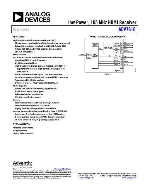
FEATURES<br />
High-Definition Multimedia Interface (<strong>HDMI</strong>®)<br />
All mandatory and additional 3D video formats supported<br />
Extended colorimetry, including sYCC601, Adobe RGB,<br />
Adobe YCC 601, and xvYCC extended gamut color<br />
CEC 1.4-compatible<br />
<strong>HDMI</strong> receiver<br />
<strong>165</strong> <strong>MHz</strong> maximum transition-minimized differential<br />
signaling (TMDS) clock frequency<br />
24-bit output pixel bus<br />
High-bandwidth Digital Content Protection (HDCP) 1.4<br />
support with internal high definition copy protocol<br />
(HDCP) keys<br />
HDCP repeater support: up to 127 KSVs supported<br />
Integrated consumer electronics control (CEC) controller<br />
Programmable <strong>HDMI</strong> equalizer<br />
5 V detect and Hot Plug assert for <strong>HDMI</strong> port<br />
Audio support<br />
S/PDIF (IEC 60958-compatible) digital audio<br />
<strong>HDMI</strong> audio extraction support<br />
Advanced audio mute feature<br />
I 2 S, 4 streams for 8 channels<br />
General<br />
Interrupt controller with two interrupt outputs<br />
Standard identification (STDI) circuit<br />
Highly flexible 24-bit pixel output interface<br />
Internal extended display identification data (EDID) RAM<br />
Any-to-any 3 × 3 color space conversion (CSC) matrix<br />
2-layer printed circuit board (PCB) design supported<br />
76-ball, 6 mm × 6 mm, chip-scale package BGA<br />
APPLICATIONS<br />
Portable applications<br />
Pico projectors<br />
Digital video cameras<br />
Rev. 0 Document Feedback<br />
Information furnished by <strong>Analog</strong> <strong>Devices</strong> is believed to be accurate and reliable. However, no<br />
responsibility is assumed by <strong>Analog</strong> <strong>Devices</strong> for its use, nor for any infringements of patents or other<br />
rights of third parties that may result from its use. Specifications subject to change without notice. No<br />
license is granted by implication or otherwise under any patent or patent rights of <strong>Analog</strong> <strong>Devices</strong>.<br />
Trademarks and registered trademarks are the property of their respective owners.<br />
<strong>HDMI</strong>1<br />
TMDS<br />
DDC<br />
FUNCTIONAL BLOCK DIAGRAM<br />
HDCP<br />
KEYS<br />
DEEP<br />
COLOR<br />
<strong>HDMI</strong> Rx<br />
36<br />
COMPONENT<br />
PROCESSOR<br />
HS/VS<br />
One Technology Way, P.O. Box 9106, Norwood, MA 02062-9106, U.S.A.<br />
Tel: 781.329.4700 ©2012 <strong>Analog</strong> <strong>Devices</strong>, Inc. All rights reserved.<br />
Technical Support www.analog.com<br />
4<br />
Figure 1.<br />
FIELD/DE<br />
LLC<br />
DATA<br />
I2S S/PDIF<br />
MCLK<br />
SCLK<br />
LRCLK<br />
OUTPUT MUX<br />
OUTPUT MUX<br />
<strong>ADV7610</strong><br />
HS<br />
VS/FIELD<br />
DE<br />
LLC<br />
24-BIT<br />
YCbCr/RGB<br />
LRCLK<br />
I2S MCLK<br />
SCLK<br />
10775-001
<strong>ADV7610</strong> Data Sheet<br />
TABLE OF CONTENTS<br />
Features .............................................................................................. 1<br />
Applications ....................................................................................... 1<br />
Functional Block Diagram .............................................................. 1<br />
Revision History ............................................................................... 2<br />
General Description ......................................................................... 3<br />
Detailed Functional Block Diagram .......................................... 3<br />
Specifications ..................................................................................... 4<br />
Electrical Characteristics ............................................................. 4<br />
Data and I 2 C Timing Characteristics ......................................... 5<br />
Absolute Maximum Ratings ............................................................ 7<br />
Package Thermal Performance ................................................... 7<br />
ESD Caution .................................................................................. 7<br />
Pin Configuration and Function Descriptions ............................. 8<br />
REVISION HISTORY<br />
12/12—Revision 0: Initial Version<br />
Rev. 0 | Page 2 of 16<br />
<strong>Power</strong> Supply Sequencing ............................................................. 10<br />
<strong>Power</strong>-Up Sequence ................................................................... 10<br />
<strong>Power</strong>-Down Sequence .............................................................. 10<br />
Functional Overview...................................................................... 11<br />
<strong>HDMI</strong> <strong>Receiver</strong> ........................................................................... 11<br />
Component Processor (CP) ...................................................... 11<br />
Other Features ............................................................................ 11<br />
Pixel Input/Output Formatting .................................................... 12<br />
Pixel Data Output Modes Features .......................................... 12<br />
Outline Dimensions ....................................................................... 14<br />
Ordering Guide .......................................................................... 14
Data Sheet <strong>ADV7610</strong><br />
GENERAL DESCRIPTION<br />
The <strong>ADV7610</strong> is offered in professional (no HDCP) and industrial<br />
versions. The operating temperature range is −40°C to +85°C.<br />
The <strong>ADV7610</strong> is a high quality, single input <strong>HDMI</strong>-capable<br />
receiver. It incorporates an <strong>HDMI</strong>-capable receiver that supports<br />
all mandatory 3D TV defined in <strong>HDMI</strong> specification. The<br />
<strong>ADV7610</strong> supports formats up to UXGA 60 Hz at eight bits.<br />
It integrates a CEC controller that supports the capability<br />
discovery and control (CDC) feature.<br />
The <strong>ADV7610</strong> has a 4-channel stereo audio output port for the<br />
audio data extracted from the <strong>HDMI</strong> stream. The <strong>HDMI</strong> receiver<br />
has an advanced mute controller that prevents audible extraneous<br />
noise in the audio output.<br />
The following audio formats are accessible:<br />
• Four streams from the I2S serializer (eight channels)<br />
• A stream from the S/PDIF serializer (two uncompressed<br />
channels or N compressed channels, for example, AC3)<br />
• A DST stream<br />
XTALP<br />
XTALN<br />
SCL<br />
SDA<br />
CEC<br />
RXA_5V<br />
HPA_A/INT2*<br />
DDCA_SDA<br />
DDCA_SCL<br />
RXA_C±<br />
RXA_0±<br />
RXA_1±<br />
RXA_2±<br />
DPLL<br />
CEC<br />
CONTROLLER<br />
5V DETECT<br />
AND HPD<br />
CONTROLLER<br />
EDID<br />
REPEATER<br />
CONTROLLER<br />
PLL<br />
EQUALIZER<br />
DETAILED FUNCTIONAL BLOCK DIAGRAM<br />
CONTROL<br />
INTERFACE<br />
I 2C<br />
SAMPLER<br />
HDCP<br />
EEPROM<br />
HDCP<br />
ENGINE<br />
CONTROL<br />
AND DATA<br />
<strong>HDMI</strong><br />
PROCESSOR<br />
DATA<br />
PREPROCESOR<br />
AND COLOR-<br />
SPACE<br />
CONVERSION<br />
PACKET<br />
PROCESSOR<br />
Rev. 0 | Page 3 of 16<br />
The <strong>HDMI</strong> port has dedicated 5 V detect and Hot Plug assert pins.<br />
The <strong>HDMI</strong> receiver also includes an integrated equalizer that<br />
ensures the robust operation of the interface with long cables.<br />
The <strong>ADV7610</strong> contains one main component processor (CP)<br />
that processes the video signals from the <strong>HDMI</strong> receiver. It<br />
provides features such as contrast, brightness, saturation<br />
adjustments, STDI detection block, free run, and synchronization<br />
alignment controls.<br />
Fabricated in an advanced CMOS process, the <strong>ADV7610</strong> is provided<br />
in a 6 mm × 6 mm, 76-ball CSP_BGA, RoHS-compliant package<br />
and is specified over the −40°C to +85°C temperature range.<br />
PACKET/<br />
INFOFRAME<br />
MEMORY<br />
BACKEND<br />
COLORSPACE<br />
CONVERSION<br />
COMPONENT<br />
PROCESSOR<br />
A<br />
B<br />
C<br />
*INT2 CAN BE OUTPUT ON ONE OF THE FOLLOWING PINS ONLY: SCLK/INT2, MCLK/INT2, OR HPA_A/INT2.<br />
Figure 2. Detailed Functional Block Diagram<br />
MUTE<br />
AUDIO<br />
PROCESSOR<br />
OUTPUT FORMATTER<br />
INTERRUPT<br />
CONTROLLER<br />
(INT1, INT2)<br />
AUDIO OUTPUT FORMATTER<br />
12<br />
12<br />
12<br />
4<br />
<strong>ADV7610</strong><br />
P0 TO P7<br />
P8 TO P15<br />
P16 TO P23<br />
LLC<br />
HS<br />
VS/FIELD/ALSB<br />
DE<br />
INT1<br />
INT2*<br />
I2S0 TO I2S3<br />
LRCLK<br />
SCLK/INT2*<br />
MCLK/INT2*<br />
10775-002
<strong>ADV7610</strong> Data Sheet<br />
SPECIFICATIONS<br />
DVDD = 1.71 V to 1.89 V, DVDDIO = 3.14 V to 3.46 V, PVDD = 1.71 V to 1.89 V, TVDD = 3.14 V to 3.46 V, CVDD = 1.71 V to 1.89 V,<br />
TMIN to TMAX = −40°C to +85°C, unless otherwise noted.<br />
ELECTRICAL CHARACTERISTICS<br />
Table 1.<br />
Parameter Symbol Test Conditions/Comments Min Typ Max Unit<br />
DIGITAL INPUTS 1<br />
Input High Voltage VIH XTALN and XTALP 1.2 V<br />
VIH Other digital inputs 2 V<br />
Input <strong>Low</strong> Voltage VIL XTALN and XTALP 0.4 V<br />
VIL Other digital inputs 0.8 V<br />
Input Current IIN RESET pin ±45 ±60 µA<br />
Other digital inputs ±10 µA<br />
Input Capacitance<br />
1, 2<br />
DIGITAL INPUTS (5 V TOLERANT)<br />
CIN 10 pF<br />
Input High Voltage VIH 2.6 V<br />
Input <strong>Low</strong> Voltage VIL 0.8 V<br />
Input Current<br />
DIGITAL OUTPUTS<br />
IIN −82 +82 µA<br />
1<br />
Output High Voltage VOH 2.4 V<br />
Output <strong>Low</strong> Voltage VOL 0.4 V<br />
High Impedance Leakage Current ILEAK VS/FIELD/ALSB pin ±35 ±60 µA<br />
HPA_A/INT2 pin ±82 µA<br />
Other 10 µA<br />
Output Capacitance<br />
POWER REQUIREMENTS<br />
COUT 20 pF<br />
3<br />
Digital Core <strong>Power</strong> Supply DVDD 1.71 1.8 1.89 V<br />
Digital I/O <strong>Power</strong> Supply DVDDIO 3.14 3.3 3.46 V<br />
PLL <strong>Power</strong> Supply PVDD 1.71 1.8 1.89 V<br />
Terminator <strong>Power</strong> Supply TVDD 3.14 3.3 3.46 V<br />
Comparator <strong>Power</strong> Supply CVDD 1.71 1.8 1.89 V<br />
Digital Core Supply Current IDVDD UXGA 60 Hz at eight bits 95.7 188.1 mA<br />
Digital I/O Supply Current IDVDDIO UXGA 60 Hz at eight bits 12.9 178.5 mA<br />
PLL Supply Current IPVDD UXGA 60 Hz at eight bits 30.7 36.9 mA<br />
Terminator Supply Current ITVDD UXGA 60 Hz at eight bits 50.9 57.6 mA<br />
Comparator Supply Current<br />
POWER-DOWN CURRENTS<br />
ICVDD UXGA 60 Hz at eight bits 95.8 114.4 mA<br />
4<br />
Digital Core Supply Current IDVDD_PD <strong>Power</strong>-Down Mode 1 0.2 0.5 mA<br />
Digital I/O Supply Current IDVDDIO_PD <strong>Power</strong>-Down Mode 1 1.3 1.7 mA<br />
PLL Supply Current IPVDD_PD <strong>Power</strong>-Down Mode 1 1.5 1.8 mA<br />
Terminator Supply Current ITVDD_PD <strong>Power</strong>-Down Mode 1 0.1 0.3 mA<br />
Comparator Supply Current ICVDD_PD <strong>Power</strong>-Down Mode 1 1.3 1.7 mA<br />
<strong>Power</strong>-Up Time tPWRUP 25 ms<br />
1 Data guaranteed by characterization.<br />
2 The following pins are 5 V tolerant: DDCA_SCL, DDCA_SDA, and RXA_5V.<br />
3 Maximum current consumption values are recorded with maximum rated voltage supply levels, Moire X video pattern, and at maximum rated temperature.<br />
4 <strong>Power</strong>-Down Mode 0 (I/O map, Register 0x0C = 0x62), ring oscillator powered down (<strong>HDMI</strong> map, Register 0x48 = 0x01), and DDC pads off (<strong>HDMI</strong> map, Register 0x73 = 0x01).<br />
Rev. 0 | Page 4 of 16
Data Sheet <strong>ADV7610</strong><br />
DATA AND I 2 C TIMING CHARACTERISTICS<br />
Table 2.<br />
Parameter Symbol Test Conditions/Comments Min Typ Max Unit<br />
CLOCK AND CRYSTAL<br />
Crystal Frequency, XTALP 28.63636 <strong>MHz</strong><br />
Crystal Frequency Stability ±50 ppm<br />
LLC Frequency Range 1 13.5 <strong>165</strong> <strong>MHz</strong><br />
I 2 C PORTS<br />
SCL Frequency 400 kHz<br />
SCL Minimum Pulse Width High 2 t1 600 ns<br />
SCL Minimum Pulse Width <strong>Low</strong> 2 t2 1.3 µs<br />
Start Condition Hold Time 2 t3 600 ns<br />
Start Condition Setup Time 2 t4 600 ns<br />
SDA Setup Time 2 t5 100 ns<br />
SCL and SDA Rise Time 2 t6 300 ns<br />
SCL and SDA Fall Time 2 t7 300 ns<br />
Stop Condition Setup Time 2 t8 0.6 µs<br />
RESET FEATURE<br />
RESET Pulse Width 5 ms<br />
CLOCK OUTPUTS<br />
LLC Mark:Space Ratio2 DATA AND CONTROL OUTPUTS<br />
t9:t10 45:55 55:45 % duty cycle<br />
3<br />
Data Output Transition Time2, 4 t11 End of valid data to negative clock edge 1.0 2.2 ns<br />
I<br />
t12 Negative clock edge to start of valid data 0.0 0.3 ns<br />
2S PORT, MASTER MODE<br />
SCLK Mark:Space Ratio2 t15:t16 45:55 55:45 % duty cycle<br />
LRCLK Data Transition Time2 t17 End of valid data to negative SCLK edge 10 ns<br />
LRCLK Data Transition Time2 t18 Negative SCLK edge to start of valid data 10 ns<br />
I2S Data Transition Time2 t19 End of valid data to negative SCLK edge 5 ns<br />
I2S Data Transition Time2 t20 Negative SCLK edge to start of valid data 5 ns<br />
1 Maximum LLC frequency is limited by the clock frequency of UXGA 60 Hz at eight bits.<br />
2 Data guaranteed by characterization.<br />
3 With the DLL block on the output clock bypassed.<br />
4 DLL bypassed on the clock path.<br />
Rev. 0 | Page 5 of 16
<strong>ADV7610</strong> Data Sheet<br />
Timing Diagrams<br />
SDA<br />
SCL<br />
SCLK<br />
LRCLK<br />
I 2S<br />
LEFT-JUSTIFIED<br />
MODE<br />
I 2S<br />
I 2 S MODE<br />
I 2S<br />
RIGHT-JUSTIFIED<br />
MODE<br />
t 3<br />
LLC<br />
P0 TO P23, HS,<br />
VS/FIELD/ALSB, DE<br />
t 15<br />
t 17<br />
t 18<br />
t 16<br />
t 2<br />
t 6<br />
t 7<br />
t 1<br />
t 5<br />
Figure 3. I 2 C Timing<br />
Figure 4. Pixel Port and Control SDR Output Timing<br />
t 19<br />
MSB MSB – 1<br />
t 20<br />
t 19<br />
t 9<br />
t 11<br />
MSB MSB – 1<br />
t 20<br />
Figure 5. I 2 S Timing<br />
Rev. 0 | Page 6 of 16<br />
t 12<br />
MSB<br />
t 10<br />
t 3<br />
t 4<br />
t 19<br />
t 8<br />
t 20<br />
LSB<br />
10775-004<br />
10775-003<br />
10775-005
Data Sheet <strong>ADV7610</strong><br />
ABSOLUTE MAXIMUM RATINGS<br />
Table 3.<br />
Parameter Rating<br />
DVDD to GND 2.2 V<br />
PVDD to GND 2.2 V<br />
DVDDIO to GND 4.0 V<br />
CVDD to GND 2.2 V<br />
TVDD to GND 4.0 V<br />
Digital Inputs Voltage to GND GND − 0.3 V to DVDDIO + 0.3 V<br />
5 V Tolerant Digital Inputs to 5.3 V<br />
GND 1<br />
Digital Outputs Voltage to GND GND − 0.3 V to DVDDIO + 0.3 V<br />
XTALP, XTALN GND − 0.3 V to PVDD + 0.3 V<br />
SCL/SDA Data Pins to DVDDIO DVDDIO − 0.3 V to<br />
DVDDIO + 3.6 V<br />
Maximum Junction Temperature<br />
(TJ MAX)<br />
125°C<br />
Storage Temperature Range −60°C to +150°C<br />
Infrared Reflow Soldering (20 sec) 260°C<br />
1 The following inputs are 3.3 V inputs but are 5 V tolerant: DDCA_SCL, DDCA_SDA,<br />
and RXA_5V.<br />
Stresses above those listed under Absolute Maximum Ratings<br />
may cause permanent damage to the device. This is a stress<br />
rating only; functional operation of the device at these or any<br />
other conditions above those indicated in the operational<br />
section of this specification is not implied. Exposure to absolute<br />
maximum rating conditions for extended periods may affect<br />
device reliability.<br />
Rev. 0 | Page 7 of 16<br />
PACKAGE THERMAL PERFORMANCE<br />
To reduce power consumption when using the <strong>ADV7610</strong>, turn<br />
off the unused sections of the part.<br />
Due to the PCB metal variation and, therefore, variation in PCB<br />
heat conductivity, the value of θJA may differ for various PCBs.<br />
The most efficient measurement solution is obtained using the<br />
package surface temperature to estimate the die temperature<br />
because this eliminates the variance associated with the θJA value.<br />
Do not exceed the maximum junction temperature (TJ MAX) of<br />
125°C. The following equation calculates the junction temperature<br />
using the measured package surface temperature, and it applies<br />
only when a heat sink is not used on the device under test (DUT):<br />
where:<br />
TJ = TS + (ΨJT × WTOTAL)<br />
TS is the package surface temperature (°C).<br />
ΨJT = 0.4°C/W for the 76-ball CSP_BGA.<br />
WTOTAL = ((PVDD × IPVDD) + (0.05 × TVDD × ITVDD) +<br />
(CVDD × ICVDD) + (DVDD × IDVDD) + (DVDDIO × IDVDDIO))<br />
where 0.05 is 5% of the TVDD power that is dissipated on the<br />
device itself.<br />
ESD CAUTION
<strong>ADV7610</strong> Data Sheet<br />
PIN CONFIGURATION AND FUNCTION DESCRIPTIONS<br />
A<br />
B<br />
C<br />
D<br />
E<br />
F<br />
G<br />
H<br />
J<br />
K<br />
1 2 3 4 5 6 7<br />
8 9 10<br />
HPA_A/<br />
INT2<br />
RXA_5V DDCA_SCL PVDD XTALN XTALP INT1<br />
TVDD TVDD DDCA_SDA CEC CS RESET SDA SCL LRCLK DVDD<br />
RXA_C+ RXA_C–<br />
I2S3 I2S1<br />
RXA_0+ RXA_0– GND GND GND DVDD<br />
I2S2 I2S0<br />
RXA_1+ RXA_1– GND<br />
DVDD<br />
Rev. 0 | Page 8 of 16<br />
MCLK/<br />
INT2<br />
SCLK/<br />
INT2<br />
VS/<br />
FIELD/<br />
ALSB<br />
RXA_2+ RXA_2– GND DVDDIO<br />
HS P0<br />
CVDD CVDD GND GND GND DVDDIO<br />
P1 P2<br />
P23 P22<br />
P3 P4<br />
P21 P18 P16 P15 P13 P11 P9<br />
P7 P5 DVDDIO<br />
P20 P19 P17 LLC P14 P12 P10<br />
P8 P6 DVDDIO<br />
Figure 6. Pin Configuration<br />
Table 4. Pin Function Descriptions<br />
Ball No. Mnemonic Type Description<br />
D4, D5, D6, E4, F4,<br />
G4, G5, G6<br />
GND Ground Ground.<br />
A1 HPA_A/INT2 Miscellaneous digital A dual function pin that can be configured to output a Hot Plug assert signal<br />
(for <strong>HDMI</strong> Port A) or an Interrupt 2 signal.<br />
G1, G2 CVDD <strong>Power</strong> <strong>HDMI</strong> <strong>Analog</strong> Block Supply Voltage (1.8 V).<br />
B1, B2 TVDD <strong>Power</strong> Terminator Supply Voltage (3.3 V).<br />
F7, G7, J10, K10 DVDDIO <strong>Power</strong> Digital I/O Supply Voltage (3.3 V).<br />
A10, B10, D7, E7 DVDD <strong>Power</strong> Digital Core Supply Voltage (1.8 V).<br />
A4 PVDD <strong>Power</strong> PLL Supply Voltage (1.8 V).<br />
C2 RXA_C− <strong>HDMI</strong> input Digital Input Clock Complement of Port A in the <strong>HDMI</strong> Interface.<br />
C1 RXA_C+ <strong>HDMI</strong> input Digital Input Clock True of Port A in the <strong>HDMI</strong> Interface.<br />
D2 RXA_0− <strong>HDMI</strong> input Digital Input Channel 0 Complement of Port A in the <strong>HDMI</strong> Interface.<br />
D1 RXA_0+ <strong>HDMI</strong> input Digital Input Channel 0 True of Port A in the <strong>HDMI</strong> Interface.<br />
E2 RXA_1− <strong>HDMI</strong> input Digital Input Channel 1 Complement of Port A in the <strong>HDMI</strong> Interface.<br />
E1 RXA_1+ <strong>HDMI</strong> input Digital Input Channel 1 True of Port A in the <strong>HDMI</strong> Interface.<br />
F2 RXA_2− <strong>HDMI</strong> input Digital Input Channel 2 Complement of Port A in the <strong>HDMI</strong> Interface.<br />
F1 RXA_2+ <strong>HDMI</strong> input Digital Input Channel 2 True of Port A in the <strong>HDMI</strong> Interface.<br />
DVDD<br />
DE<br />
10775-006
Data Sheet <strong>ADV7610</strong><br />
Ball No. Mnemonic Type Description<br />
H1 P23 Digital video output Video Pixel Output Port.<br />
H2 P22 Digital video output Video Pixel Output Port.<br />
J1 P21 Digital video output Video Pixel Output Port.<br />
K1 P20 Digital video output Video Pixel Output Port.<br />
K2 P19 Digital video output Video Pixel Output Port.<br />
J2 P18 Digital video output Video Pixel Output Port.<br />
K3 P17 Digital video output Video Pixel Output Port.<br />
J3 P16 Digital video output Video Pixel Output Port.<br />
K4 LLC Digital video output Line Locked Output Clock for the Pixel Data the Range is 13.5 <strong>MHz</strong> to 162.5 <strong>MHz</strong>.<br />
J4 P15 Digital video output Video Pixel Output Port.<br />
K5 P14 Digital video output Video Pixel Output Port.<br />
J5 P13 Digital video output Video Pixel Output Port.<br />
K6 P12 Digital video output Video Pixel Output Port.<br />
J6 P11 Digital video output Video Pixel Output Port.<br />
K7 P10 Digital video output Video Pixel Output Port.<br />
J7 P9 Digital video output Video Pixel Output Port.<br />
K8 P8 Digital video output Video Pixel Output Port.<br />
J8 P7 Digital video output Video Pixel Output Port.<br />
K9 P6 Digital video output Video Pixel Output Port.<br />
J9 P5 Digital video output Video Pixel Output Port.<br />
H10 P4 Digital video output Video Pixel Output Port.<br />
H9 P3 Digital video output Video Pixel Output Port.<br />
G10 P2 Digital video output Video Pixel Output Port.<br />
G9 P1 Digital video output Video Pixel Output Port.<br />
F10 P0 Digital video output Video Pixel Output Port.<br />
E10 DE Miscellaneous digital Data Enable. DE is a signal that indicates active pixel data.<br />
F9 HS Digital video output Horizontal Synchronization Output Signal.<br />
E9 VS/FIELD/ALSB Digital input/output Vertical Synchronization Output Signal.<br />
Field Synchronization Output Signal in All Interlaced Video Modes.<br />
VS or FIELD can be configured for this pin.<br />
The ALSB allows selection of the I 2 C address.<br />
D10, C10, D9, C9 I2S0 to I2S3 Miscellaneous digital Audio Output Pins. These pins can be configured to output S/PDIF digital<br />
audio (S/PDIF) or I 2 S.<br />
A9 SCLK/INT2 Miscellaneous digital A dual function pin that can be configured to output an audio serial clock or<br />
an Interrupt 2 signal.<br />
B9 LRCLK Miscellaneous digital Audio Left/Right Clock.<br />
A8 MCLK/INT2 Miscellaneous digital A dual function pin that can be configured to output an audio master clock or<br />
an Interrupt 2 signal.<br />
B8 SCL Miscellaneous digital I 2 C Port Serial Clock Input. SCL is the clock line for the control port.<br />
B7 SDA Miscellaneous digital I 2 C Port Serial Data Input/Output Pin. SDA is the data line for the control port.<br />
A7 INT1 Miscellaneous digital Interrupt 1. This pin can be active low or active high. When status bits change, this<br />
pin is triggered. The events that trigger an interrupt are under user configuration.<br />
B6 RESET Miscellaneous digital System Reset Input. Active low. A minimum low reset pulse width of 5 ms is<br />
required to reset the <strong>ADV7610</strong> circuitry.<br />
A6 XTALP Miscellaneous analog Input Pin for 28.63636 <strong>MHz</strong> Crystal or an External 1.8 V, 28.63636 <strong>MHz</strong> Clock<br />
Oscillator Source to Clock the <strong>ADV7610</strong>.<br />
A5 XTALN Miscellaneous analog Crystal Input. Input pin for 28.63636 <strong>MHz</strong> crystal.<br />
B4 CEC Digital input/output Consumer Electronic Control Channel.<br />
B5 CS Miscellaneous digital Chip Select (Bar). Pulling this line high causes the I 2 C state machine to ignore<br />
the I 2 C transmission.<br />
A3 DDCA_SCL <strong>HDMI</strong> input HDCP Slave Serial Clock Port A. DDCA_SCL is a 3.3 V input that is 5 V tolerant.<br />
B3 DDCA_SDA <strong>HDMI</strong> input HDCP Slave Serial Data Port A. DDCA_SDA is a 3.3 V input that is 5 V tolerant.<br />
A2 RXA_5V <strong>HDMI</strong> input 5 V Detect Pin for Port A in the <strong>HDMI</strong> Interface.<br />
Rev. 0 | Page 9 of 16
<strong>ADV7610</strong> Data Sheet<br />
POWER SUPPLY SEQUENCING<br />
POWER-UP SEQUENCE<br />
The recommended power-up sequence of the <strong>ADV7610</strong> is to<br />
power up the 3.3 V supplies first, followed by the 1.8 V supplies.<br />
Hold reset low while the supplies are powered up.<br />
Alternatively, the <strong>ADV7610</strong> can be powered up by asserting all<br />
supplies simultaneously. In this case, care must be taken while the<br />
supplies are being established to ensure that a lower rated supply<br />
does not rise above a higher rated supply level.<br />
POWER-DOWN SEQUENCE<br />
The <strong>ADV7610</strong> supplies can be deasserted simultaneously as long as<br />
a higher rated supply does not fall below a lower rated supply.<br />
Rev. 0 | Page 10 of 16<br />
POWER SUPPLY (V)<br />
3.3V<br />
1.8V<br />
3.3V SUPPLIES<br />
1.8V SUPPLIES<br />
3.3V SUPPLIES 1.8V SUPPLIES<br />
POWER-UP POWER-UP<br />
10775-007<br />
Figure 7. Recommended <strong>Power</strong>-Up Sequence
Data Sheet <strong>ADV7610</strong><br />
FUNCTIONAL OVERVIEW<br />
<strong>HDMI</strong> RECEIVER<br />
The receiver supports all mandatory and many optional 3D<br />
formats. It supports HDTV formats up to UXGA at eight bits.<br />
The <strong>HDMI</strong>-compatible receiver on the <strong>ADV7610</strong> incorporates<br />
programmable equalization of the <strong>HDMI</strong> data signals. This<br />
equalization compensates for the high frequency losses inherent<br />
in <strong>HDMI</strong> and DVI cabling, especially at longer lengths and higher<br />
frequencies. It is capable of equalizing for cable lengths of up to<br />
30 meters to achieve robust receiver performance.<br />
With the inclusion of HDCP, displays can receive encrypted<br />
video content. The <strong>HDMI</strong> interface of the <strong>ADV7610</strong> allows for<br />
authentication of a video receiver, decryption of encoded data at<br />
the receiver, and renewability of that authentication during<br />
transmission, as specified by the HDCP 1.4 protocol.<br />
The <strong>ADV7610</strong> has a synchronization regeneration block to<br />
regenerate the DE based on the measurement of the video<br />
format being displayed and to filter the horizontal and vertical<br />
synchronization signals to prevent glitches. The <strong>HDMI</strong> receiver<br />
also supports TERC4 error detection for detection of corrupted<br />
<strong>HDMI</strong> packets following a cable disconnect.<br />
The <strong>HDMI</strong> receiver contains an audio mute controller that can<br />
detect a variety of conditions that may result in audible extraneous<br />
noise in the audio output. On detection of these conditions, the<br />
audio signal can be ramped to prevent audio clicks or pops.<br />
Audio output can be formatted to LPCM and IEC 61937.<br />
The <strong>HDMI</strong> receiver features include:<br />
• 162.5 <strong>MHz</strong> (UXGA at eight bits) maximum TMDS clock<br />
frequency<br />
• 3D format support defined in the <strong>HDMI</strong> specification<br />
• Integrated equalizer for cable lengths of up to 30 meters<br />
• HDCP 1.4<br />
• Internal HDCP keys<br />
• PCM audio packet support<br />
• TDM I2S audio packet support<br />
• Repeater support<br />
• Internal EDID RAM<br />
• Hot Plug assert output pin for an <strong>HDMI</strong> port<br />
• CEC controller<br />
Rev. 0 | Page 11 of 16<br />
COMPONENT PROCESSOR (CP)<br />
The <strong>ADV7610</strong> has an any-to-any 3 × 3 CSC matrix. The CSC<br />
block is placed in the output section of the component processor.<br />
The CSC enables YPrPb-to-RGB and RGB-to-YCrCb conversions.<br />
Many other standards of colorspace can be implemented using<br />
the colorspace converter.<br />
CP features include:<br />
• 525i, 625i, 525p, 625p, 720p, 1080i, 1080p, and other formats<br />
• Manual adjustments including gain (contrast) and offset<br />
(brightness), hue, and saturation<br />
• Free run output mode that provides stable timing when no<br />
video input is present<br />
• 162.5 <strong>MHz</strong> processing rate<br />
• Contrast, brightness, hue, and saturation controls<br />
• Standard identification enabled by STDI block<br />
• RGB that can be color space converted to YCrCb and<br />
decimated to a 4:2:2 format for videocentric back-end IC<br />
interfacing<br />
• DE output signal supplied for direct connection to an<br />
<strong>HDMI</strong>/DVI transmitter<br />
OTHER FEATURES<br />
The <strong>ADV7610</strong> has HS, VS, FIELD, and DE output signals with<br />
programmable position, polarity, and width.<br />
The <strong>ADV7610</strong> has programmable interrupt request output pins,<br />
including INT1 and INT2 (INT2 is accessible only via one of<br />
following pins: MCLK/INT2, SCLK/INT2, or HPA_A/INT2).<br />
It also features a low power-down mode. The I2C address of the<br />
main map is 0x98 after reset. This can be changed after reset to<br />
0x9A if pull-up is attached to the VS/FIELD/ALSB pin and the<br />
I2C command SAMPLE_ALSB is issued.<br />
The <strong>ADV7610</strong> is provided in a 6 mm × 6 mm, RoHS-compliant<br />
BGA package and is specified over the −40°C to +85°C<br />
temperature range.<br />
For more detailed product information about the <strong>ADV7610</strong>,<br />
contact the local <strong>Analog</strong> <strong>Devices</strong>, Inc., sales office.
<strong>ADV7610</strong> Data Sheet<br />
PIXEL INPUT/OUTPUT FORMATTING<br />
The output section of the <strong>ADV7610</strong> is highly flexible. The pixel<br />
output bus can support up to 24-bit 4:4:4 YCrCb. The pixel data<br />
supports both single data rate mode and double data rate mode. In<br />
SDR mode, a 16-/24-bit 4:2:2 or 24-bit 4:4:4 output is possible.<br />
In DDR mode, the pixel output port can be configured in an 8-/12bit<br />
4:2:2 YCrCb or 24-bit 4:4:4 RGB.<br />
Bus rotation is supported. Table 5 and Table 6 outline the various<br />
output formats that are supported. All output modes are controlled<br />
via I 2 C.<br />
Rev. 0 | Page 12 of 16<br />
PIXEL DATA OUTPUT MODES FEATURES<br />
The output pixel port features include:<br />
• 8-/12-bit ITU-R BT.656 4:2:2 YCrCb with embedded time<br />
codes and/or HS, VS, and FIELD output signals<br />
• 16-/24-bit YCrCb with embedded time codes and/or HS<br />
and VS/FIELD pin timing<br />
• 24-bit YCrCb/RGB with embedded time codes and/or HS<br />
and VS/FIELD pin timing<br />
• DDR 8-/12-bit 4:2:2 YCrCb<br />
• DDR 24-bit 4:4:4 RGB<br />
Table 5. SDR 4:2:2 and 4:4:4 Output Modes<br />
SDR 4:2:2 SDR 4:4:4<br />
OP_FORMAT_SEL[7:0] 0x0 0x0A 0x80 0x8A 0x40<br />
Pixel Output<br />
8-Bit SDR<br />
ITU-R BT.656<br />
Mode 0<br />
12-Bit SDR<br />
ITU-R BT.656<br />
Mode 2<br />
16-Bit SDR<br />
ITU-R BT.656 4:2:2<br />
Mode 0<br />
24-Bit SDR<br />
ITU-R BT.656 4:2:2<br />
Mode 2<br />
P23 High-Z Y3, Cb3, Cr3 High-Z Y3 R7<br />
P22 High-Z Y2, Cb2, Cr2 High-Z Y2 R6<br />
P21 High-Z Y1, Cb1, Cr1 High-Z Y1 R5<br />
P20 High-Z Y0, Cb0, Cr0 High-Z Y0 R4<br />
P19 High-Z High-Z High-Z Cb3, Cr3 R3<br />
P18 High-Z High-Z High-Z Cb2, Cr2 R2<br />
P17 High-Z High-Z High-Z Cb1, Cr1 R1<br />
P16 High-Z High-Z High-Z Cb0, Cr0 R0<br />
P15 Y7, Cb7, Cr7 Y11, Cb11, Cr11 Y7 Y11 G7<br />
P14 Y6, Cb6, Cr6 Y10, Cb10, Cr10 Y6 Y10 G6<br />
P13 Y5, Cb5, Cr5 Y9, Cb9, Cr9 Y5 Y9 G5<br />
P12 Y4, Cb4, Cr4 Y8, Cb8, Cr8 Y4 Y8 G4<br />
P11 Y3, Cb3, Cr3 Y7, Cb7, Cr7 Y3 Y7 G3<br />
P10 Y2, Cb2, Cr2 Y6, Cb6, Cr6 Y2 Y6 G2<br />
P9 Y1, Cb1, Cr1 Y5, Cb5, Cr5 Y1 Y5 G1<br />
P8 Y0, Cb0, Cr0 Y4, Cb4, Cr4 Y0 Y4 G0<br />
P7 High-Z High-Z Cb7, Cr7 Cb11, Cr11 B7<br />
P6 High-Z High-Z Cb6, Cr6 Cb10, Cr10 B6<br />
P5 High-Z High-Z Cb5, Cr5 Cb9, Cr9 B5<br />
P4 High-Z High-Z Cb4, Cr4 Cb8, Cr8 B4<br />
P3 High-Z High-Z Cb3, Cr3 Cb7, Cr7 B3<br />
P2 High-Z High-Z Cb2, Cr2 Cb6, Cr6 B2<br />
P1 High-Z High-Z Cb1, Cr1 Cb5, Cr5 B1<br />
P0 High-Z High-Z Cb0, Cr0 Cb4, Cr4 B0<br />
24-Bit SDR 4:4:4<br />
Mode 0
Data Sheet <strong>ADV7610</strong><br />
Table 6. DDR 4:2:2 and 4:4:4 Output Modes<br />
DDR 4:2:2 Mode (Clock/2) DDR 4:2:2 Mode (Clock/2) 1, 2<br />
DDR 4:4:4 Mode (Clock/2)<br />
OP_FORMAT_SEL[7:0] 0x20 0x2A 0x60<br />
8-Bit DDR ITU-656<br />
(Clock/2 Output) 4:2:2 Mode 0<br />
12-Bit DDR ITU-656<br />
(Clock/2 Output) 4:2:2 Mode 2<br />
Rev. 0 | Page 13 of 16<br />
24-Bit DDR RGB<br />
(Clock/2 Output)<br />
Pixel Output Clock Rise Clock Fall Clock Rise Clock Fall Clock Rise Clock Fall<br />
P23 High-Z High-Z Cb3, Cr3 Y3 R7-0 R7-1<br />
P22 High-Z High-Z Cb2, Cr2 Y2 R6-0 R6-1<br />
P21 High-Z High-Z Cb1, Cr1 Y1 R5-0 R5-1<br />
P20 High-Z High-Z Cb0, Cr0 Y0 R4-0 R4-1<br />
P19 High-Z High-Z High-Z High-Z R3-0 R3-1<br />
P18 High-Z High-Z High-Z High-Z R2-0 R2-1<br />
P17 High-Z High-Z High-Z High-Z R1-0 R1-1<br />
P16 High-Z High-Z High-Z High-Z R0-0 R0-1<br />
P15 Cb7, Cr7 Y7 Cb11, Cr11 Y11 G7-0 G7-1<br />
P14 Cb6, Cr6 Y6 Cb12, Cr12 Y12 G6-0 G6-1<br />
P13 Cb5, Cr5 Y5 Cb9, Cr9 Y9 G5-0 G5-1<br />
P12 Cb4, Cr4 Y4 Cb8, Cr8 Y8 G4-0 G4-1<br />
P11 Cb3, Cr3 Y3 Cb7, Cr7 Y7 G3-0 G3-1<br />
P10 Cb2, Cr2 Y2 Cb6, Cr6 Y6 G2-0 G2-1<br />
P9 Cb1, Cr1 Y1 Cb5, Cr5 Y5 G1-0 G1-1<br />
P8 Cb0, Cr0 Y0 Cb4, Cr4 Y4 G0-0 G0-1<br />
P7 High-Z High-Z High-Z High-Z B7-0 B7-1<br />
P6 High-Z High-Z High-Z High-Z B6-0 B6-1<br />
P5 High-Z High-Z High-Z High-Z B5-0 B5-1<br />
P4 High-Z High-Z High-Z High-Z B4-0 B4-1<br />
P3 High-Z High-Z High-Z High-Z B3-0 B3-1<br />
P2 High-Z High-Z High-Z High-Z B2-0 B2-1<br />
P1 High-Z High-Z High-Z High-Z B1-0 B1-1<br />
P0 High-Z High-Z High-Z High-Z B0-0 B0-1<br />
1 -0 = even samples.<br />
2 -1 = odd samples.
<strong>ADV7610</strong> Data Sheet<br />
OUTLINE DIMENSIONS<br />
ORDERING GUIDE<br />
*1.40 MAX<br />
6.10<br />
6.00 SQ<br />
5.90<br />
BALL A1<br />
PAD CORNER<br />
TOP VIEW<br />
DETAIL A<br />
4.50<br />
BSC SQ<br />
0.50<br />
BSC<br />
0.15 MIN<br />
0.75<br />
REF<br />
*COMPLIANT TO JEDEC STANDARDS MO-225<br />
WITH THE EXCEPTION TO PACKAGE HEIGHT.<br />
Rev. 0 | Page 14 of 16<br />
A1 CORNER<br />
INDEX AREA<br />
10 9 8 7 6 5 4 3 2 1<br />
BOTTOM VIEW<br />
DETAIL A<br />
0.35<br />
SEATING<br />
0.30 PLANE<br />
0.25<br />
BALL DIAMETER<br />
Figure 8. 76-Ball Chip Scale Package Ball Grid Array [CSP_BGA]<br />
(BC-76-1)<br />
Dimensions shown in millimeters<br />
A<br />
B<br />
C<br />
D<br />
E<br />
F<br />
G<br />
H<br />
J<br />
K<br />
0.65 MIN<br />
COPLANARITY<br />
0.08 MAX<br />
Model 1<br />
Temperature<br />
Package<br />
Range Package Description<br />
Option<br />
<strong>ADV7610</strong>BBCZ −40°C to +85°C 76-Ball Chip Scale Package Ball Grid Array [CSP_BGA] BC-76-1<br />
<strong>ADV7610</strong>BBCZ-RL −40°C to +85°C 76-Ball Chip Scale Package Ball Grid Array [CSP_BGA], 13” Tape and Reel BC-76-1<br />
<strong>ADV7610</strong>BBCZ-P −40°C to +85°C 76-Ball Chip Scale Package Ball Grid Array [CSP_BGA], NonHDCP Version BC-76-1<br />
<strong>ADV7610</strong>BBCZ-P-RL −40°C to +85°C 76-Ball Chip Scale Package Ball Grid Array [CSP_BGA], 13” Tape and Reel, NonHDCP Version BC-76-1<br />
1 Z = RoHS Compliant Part.<br />
010807-A
Data Sheet <strong>ADV7610</strong><br />
NOTES<br />
Rev. 0 | Page 15 of 16
<strong>ADV7610</strong> Data Sheet<br />
NOTES<br />
The terms <strong>HDMI</strong> and <strong>HDMI</strong> High-Definition Multimedia Interface, and the <strong>HDMI</strong> logo are trademarks or registered trademarks of <strong>HDMI</strong> Licensing LLC in the United<br />
States and other countries.<br />
©2012 <strong>Analog</strong> <strong>Devices</strong>, Inc. All rights reserved. Trademarks and<br />
registered trademarks are the property of their respective owners.<br />
D10775-0-12/12(0)<br />
Rev. 0 | Page 16 of 16


