Photo Lithography.ppt - 123SeminarsOnly
Photo Lithography.ppt - 123SeminarsOnly
Photo Lithography.ppt - 123SeminarsOnly
You also want an ePaper? Increase the reach of your titles
YUMPU automatically turns print PDFs into web optimized ePapers that Google loves.
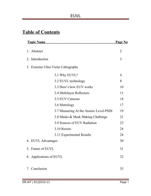
Table of Contents<br />
Topic Name<br />
EUVL<br />
Page No<br />
1. Abstract 2<br />
2. Introduction 3<br />
3. Extreme Ultra Violet <strong>Lithography</strong><br />
3.1 Why EUVL? 4<br />
3.2 EUVL technology 8<br />
3.3 Here’s how EUV works 10<br />
3.4 Multilayer Reflectors 11<br />
3.5 EUV Cameras 14<br />
3.6 Metrology 17<br />
3.7 Measuring At the Atomic Level-PSDI 19<br />
3.8 Masks & Mask Making Challenge 21<br />
3.9 Sources of EUV Radiation 23<br />
3.10 Resists 24<br />
3.11 Experimental Results 24<br />
4. EUVL Advantages 30<br />
5. Future of EUVL 31<br />
6. Applications of EUVL 32<br />
7. Conclusion 33<br />
DR.AIT | EC|2010-11 Page 1
EUVL<br />
8. References 34<br />
Chapter 1<br />
ABSTRACT<br />
This paper discusses the basic concepts and current state of development of EUV<br />
lithography (EUVL), a relatively new form of lithography that uses extreme ultraviolet<br />
(EUV) radiation with a wavelength in the range of 10 to 14 nanometers (nm) to carry out<br />
projection imaging. Currently, and for the last several decades, optical projection<br />
lithography has been the lithographic technique used in the high-volume manufacture of<br />
integrated circuits.<br />
It is widely anticipated that improvements in this technology will allow it to<br />
remain the semiconductor industry's workhorse through the 100 nm generation of<br />
devices. However, sometime around the year 2005, so-called Next-Generation<br />
Lithographies will be required. EUVL is one such technology vying to become the<br />
successor to optical lithography. This paper provides an overview of the capabilities of<br />
EUVL, and explains how EUVL might be implemented. The challenges that must be<br />
overcome in order for EUVL to qualify for high-volume manufacture are also discussed.<br />
This approach uses a laser-produced plasma source of radiation, a<br />
reflective mask, and a 4_ reduction all-reflective imaging system. The technology is<br />
currently in the engineering development phase for an alpha machine. This paper reviews<br />
DR.AIT | EC|2010-11 Page 2
EUVL<br />
its current status and describes the basic modules or building blocks of a generic EUVL<br />
exposure tool.<br />
Chapter 2<br />
Index Terms— <strong>Lithography</strong>, semiconductor device manufacture<br />
INTRODUCTION<br />
Microprocessors, also called computer chips, are made using a process called<br />
lithography. Specifically, deep-ultraviolet lithography is used to make the current breed<br />
of microchips and was most likely used to make the chip that is inside your computer.<br />
<strong>Lithography</strong> is akin to photography in that it uses light to transfer images onto a<br />
substrate. Silicon is the traditional substrate used in chip making. To create the integrated<br />
circuit design that's on a microprocessor, light is directed onto a mask. A mask is like a<br />
stencil of the circuit pattern. The light shines through the mask and then through a series<br />
of optical lenses that shrink the image down. This small image is then projected onto a<br />
silicon, or semiconductor, wafer. The wafer is covered with a light-sensitive, liquid<br />
plastic called photoresist. The mask is placed over the wafer, and when light shines<br />
through the mask and hits the silicon wafer, it hardens the photoresist that isn't covered<br />
by the mask. The photoresist that is not exposed to light remains somewhat gooey and is<br />
chemically washed away, leaving only the hardened photoresist and exposed silicon<br />
wafer.<br />
The key to creating more powerful microprocessors is the size of the light's<br />
wavelength. The shorter the wavelength, the more transistors can be etched onto the silicon<br />
wafer. More transistors equal a more powerful, faster microprocessor.<br />
Deep-ultraviolet lithography uses a wavelength of 240 nanometers As chipmakers reduce<br />
to smaller wavelengths, they will need a new chip making technology. The problem posed<br />
by using deep-ultraviolet lithography is that as the light's wavelengths get smaller, the light<br />
gets absorbed by the glass lenses that are intended to focus it. The result is that the light<br />
DR.AIT | EC|2010-11 Page 3
EUVL<br />
doesn't make it to the silicon, so no circuit pattern is created on the wafer. This is where<br />
EUVL (Extreme Ultraviolet Lithogrphy) will take over. In EUVL, glass lenses will be<br />
replaced by mirrors to focus light and thus EUV lithography can make use of smaller wave<br />
lengths. Hence more and more transistors can be packed into the chip. The result is that<br />
using EUV lithography, we can make chips that are upto 100 times faster than today’s<br />
chips with similar increase in storage capacity.<br />
Chapter 3<br />
EXTREME ULTRAVIOLET LITHOGRAPHY<br />
3.1 WHY EUVL?<br />
In order to keep pace with the demand for the printing of ever smaller features,<br />
lithography tool manufacturers have found it necessary to gradually reduce the<br />
wavelength of the light used for imaging and to design imaging systems with ever larger<br />
numerical apertures. The reasons for these changes can be understood from the following<br />
equations that describe two of the most fundamental characteristics of an imaging system:<br />
its resolution (RES) and depth of focus (DOF). These equations are usually expressed as<br />
RES = k1 λ / NA (1a)<br />
and<br />
DOF = k2 λ / (NA) 2 , (1b)<br />
Where λ is the wavelength of the radiation used to carry out the imaging, and NA is the<br />
numerical aperture of the imaging system (or camera). These equations show that better<br />
resolution can be achieved by reducing λ and increasing NA. The penalty for doing this,<br />
however, is that the DOF is decreased. Until recently, the DOF used in manufacturing<br />
exceeded 0.5 um, which provided for sufficient process control.<br />
The case k1 = k2 = ½ corresponds to the usual definition of diffraction-limited<br />
imaging. In practice, however, the acceptable values for k1 and k2 are determined<br />
DR.AIT | EC|2010-11 Page 4
EUVL<br />
experimentally and are those values which yield the desired control of critical dimensions<br />
(CD's) within a tolerable process window. Camera performance has a major impact on<br />
determining these values; other factors that have nothing to do with the camera also play<br />
a role. Such factors include the contrast of the resist being used and the characteristics of<br />
any etching processes used. Historically, values for k1 and k2 greater than 0.6 have been<br />
used comfortably in high-volume manufacture. Recently, however, it has been necessary<br />
to extend imaging technologies to ever better resolution by using smaller values for k1<br />
and k2 and by accepting the need for tighter process control. This scenario is<br />
schematically diagrammed in Figure 2.1, where the values for k1 and DOF associated<br />
with lithography using light at 248 nm and 193 nm to print past, present, and future CD's<br />
ranging from 350 nm to 100 nm are shown. The "Comfort Zone for Manufacture"<br />
corresponds to the region for which k1 > 0.6 and DOF > 0.5 um. Also shown are the k1<br />
and DOF values currently associated with the EUVL printing of 100 nm features, which<br />
will be explained later. As shown in the figure, in the very near future it will be necessary<br />
to utilize k1 values that are considerably less than 0.5. Problems associated with small k1<br />
values include a large iso/dense bias (different conditions needed for the proper printing<br />
of isolated and dense features), poor CD control, nonlinear printing (different conditions<br />
needed for the proper printing of large and small features), and magnification of mask<br />
CD errors. Figure 2.1 also shows that the DOF values associated with future lithography<br />
will be uncomfortably small. Of course, resolution enhancement techniques such as<br />
phase-shift masks, modified illumination schemes, and optical proximity correction can<br />
be used to enhance resolution while increasing the effective DOF. However, these<br />
techniques are not generally applicable to all feature geometries and are difficult to<br />
DR.AIT | EC|2010-11 Page 5
EUVL<br />
implement in manufacturing. The degree to which these techniques can be employed in<br />
manufacturing will determine how far optical lithography can be extended before an<br />
NGL is needed<br />
Figure 2.1:The k1 and DOF values associated with 248 nm and 193 nm lithographies for<br />
the printing of CD values ranging from 350 nm down to 100 nm assuming that k2 = k1 and<br />
NA = 0.6<br />
EUVL alleviates the foregoing problems by drastically decreasing the wavelength<br />
used to carry out imaging. Consider Figure 2. The dashed black<br />
DR.AIT | EC|2010-11 Page 6
EUVL<br />
line shows the locus of points corresponding to a resolution of 100 nm; the region<br />
to the right of the line corresponds to even better resolution.<br />
Figure 2.2: The region between the lines shows the wavelength and numerical aperture of<br />
cameras simultaneously having a resolution of 100 nm or better and a DOF of 0.5 um or<br />
better.<br />
The solid red line shows the locus of points for which the DOF is 0.5 um; in the region<br />
to the left of that line the DOF values are larger. Points in the region between the two<br />
lines correspond to situations in which the resolution is 100 nm or better, and the DOF is<br />
0.5 um or longer. As shown, to be in this favorable region, the wavelength of the light<br />
used for imaging must be less than 40 nm, and the NA of the imaging system must be<br />
less than 0.2. The solid circle shows the parameters used in current imaging experiments.<br />
Light having wavelengths in the spectral region from 40 nm to 1 nm is variously referred<br />
to as extreme UV, vacuum UV, or soft x-ray radiation. Projection lithography carried out<br />
with light in this region has come to be known as EUV lithography (EUVL). Early in the<br />
development of EUVL, the technology was called soft x-ray projection lithography<br />
DR.AIT | EC|2010-11 Page 7
EUVL<br />
(SXPL), but that name was dropped in order to avoid confusion with x-ray lithography,<br />
which is a 1:1, near-contact printing technology<br />
DR.AIT | EC|2010-11 Page 8
As explained above, EUVL is capable of printing features of 100 nm and smaller while<br />
achieving a DOF of 0.5 um and larger. Currently, most EUVL work is carried out in a<br />
wavelength region around 13 nm using cameras that have an NA of about 0.1, which<br />
places the technology well within the "Comfort Zone for Manufacture" as shown in<br />
Figure 2.1 by the data point farthest to the right.<br />
3.2 EUVL TECHNOLOGY<br />
In many respects, EUVL retains the look and feel of optical lithography as<br />
practiced today. For example, the basic optical design tools that are used for EUV<br />
imaging system design and for EUV image simulations are also used today for optical<br />
projection lithography. Nonetheless, in other respects EUVL technology is very different<br />
from what the industry is familiar with. Most of these differences arise because the<br />
properties of materials in the EUV are very different from their properties in the visible<br />
and UV ranges.<br />
Foremost among those differences is the fact that EUV radiation is strongly<br />
absorbed in virtually all materials, even gases. EUV imaging must be carried out in a near<br />
vacuum. Absorption also rules out the use of refractive optical elements, such as lenses<br />
and transmission masks. Thus EUVL imaging systems are entirely reflective. Ironically,<br />
the EUV reflectivity of individual materials at near-normal incidence is very low. In<br />
order to achieve reasonable reflectivities near normal incidence, surfaces must be coated<br />
with multilayer, thin-film coatings known as distributed Bragg reflectors. The best of<br />
these function in the region between 11 and 14 nm. EUV absorption in standard optical
photoresists is very high, and new resist and processing techniques will be required for<br />
application in EUVL.<br />
Because EUVL utilizes short wavelength radiation for imaging, the mirrors that<br />
comprise the camera will be required to exhibit an unprecedented degree of perfection in<br />
surface figure and surface finish in order to achieve diffraction-limited imaging.<br />
Fabrication of mirrors exhibiting such perfection will require new and more accurate<br />
polishing and metrology techniques.<br />
Clearly, then, there are a number of new technology problems that arise<br />
specifically because of the use of EUV radiation. Intel has formed a<br />
consortium called the EUV, LLC (the LLC), which currently also includes AMD and<br />
Motorola, to support development of these EUV-specific technologies. The bulk of this<br />
development work is carried out by three national laboratories functioning as a single<br />
entity called the Virtual National Laboratory (VNL). Participants in the VNL are<br />
Lawrence Livermore National Laboratory, Sandia National Laboratories, and Lawrence<br />
Berkeley National Laboratory. Development work is also carried out by LLC members,<br />
primarily on mask fabrication and photoresist development. Recently, additional support<br />
for some of this work has come from Sematech. The work described in the following<br />
sections was carried out within this program, primarily by workers within the VNL.
3.3 HERE'S HOW EUVL WORKS<br />
1<br />
2<br />
3<br />
1. A laser is directed at a jet of xenon gas. When the laser hits the xenon gas, it heats the<br />
gas up and creates plasma.<br />
4<br />
2. Once the plasma is created, electrons begin to come off of it and it radiates light at 13<br />
nanometers, which is too short for the human eye to see.
3. The light travels into a condenser, which gathers in the light so that it is directed onto<br />
the mask.<br />
4. A representation of one level of a computer chip is patterned onto a mirror by applying<br />
an absorber to some parts of the mirror but not to others. This creates the mask.<br />
5. The pattern on the mask is reflected onto a series of four to six curved mirrors,<br />
reducing the size of the image and focusing the image onto the silicon wafer. Each mirror<br />
bends the light slightly to form the image that will be transferred onto the wafer. This is<br />
just like how the lenses in your camera bend light to form an image on film.<br />
3.4 MULTILAYER REFLECTORS<br />
In order to achieve reasonable reflectivities, the reflecting surfaces in EUVL<br />
imaging systems are coated with multilayer thin films (ML's). These coatings consist of a<br />
large number of alternating layers of materials having dissimilar EUV optical constants,<br />
and they provide a resonant reflectivity when the period of the layers is approximately λ /<br />
2. Without such reflectors, EUVL would not be possible. On the other hand, the resonant<br />
behavior of ML's complicates the design, analysis, and fabrication of EUV cameras. The<br />
most developed and best understood EUV multilayers are made of alternating layers of<br />
Mo and Si, and they function best for wavelengths of about 13 nm. Figure 2.3 shows the<br />
reflectivity and phase change upon reflection for an MoSi ML that has been optimized for<br />
peak reflectivity at 13.4 nm at normal incidence; similar resonance behavior is seen as a<br />
function of angle of incidence for a fixed wavelength. While the curve shown is<br />
theoretical, peak reflectivites of 68% can now be routinely attained for MoSi ML's<br />
deposited by magnetron sputtering.
Figure 2.3: Curve showing the normal incidence reflectivity and phase upon reflection of<br />
an MoSi ML as a function of wavelength; the coating was designed to have peak<br />
reflectivity at 13.4 nm<br />
This resonance behavior has important implications for EUVL. A typical EUVL<br />
camera is composed of at least four mirrors, and light falls onto the various mirrors over<br />
different angular ranges. As a consequence, the periods of the ML's applied to the various<br />
mirrors must be different so that all the mirrors are tuned to reflect the same wavelength.<br />
Proper matching of the peak wavelengths is crucial for achieving high radiation<br />
throughput and good imaging performance. The range of angles of incidence over a<br />
single mirror surface must also be considered. For some optical designs, the angular<br />
ranges are small enough that ML's with a uniform period over the surface can be used. In
other designs, the angular ranges are so large that the ML period must be accurately<br />
varied over the surface in order to achieve uniform reflectivity. There are optical designs<br />
in which the angular ranges are so large that ML reflectors can not be utilized.<br />
The effects on imaging performance due to the variations of ML reflectivity and<br />
phase with wavelength and angle have been extensively modeled. The effects have been<br />
shown to be minimal for cameras of interest to us. The primary perturbations of the<br />
wavefront transmitted by the camera are described as a simple tilt and defocus.<br />
Two types of EUV cameras are fabricated. The first is a small field, microstepper-<br />
like design that utilizes two mirrors and those images with a reduction factor of 10. We<br />
call it the "10X camera." This camera has been used extensively in our early<br />
investigations of EUV imaging. One of the mirrors in this camera requires a strongly<br />
graded ML coating. Three of these cameras have been fabricated and have been shown to<br />
perform well. (Examples of the imaging performance of these cameras are shown later in<br />
this paper.) The second camera, currently being fabricated, is a prototype lithography<br />
camera with a ring field of 26 mm X 1.5 mm. This camera was designed so that it will<br />
perform well with uniform ML coatings. The VNL has demonstrated the ability to<br />
achieve the ML matching, uniformity, and grading requirements of EUVL cameras<br />
currently of interest.
3.5 EUV CAMERAS<br />
Designing an all-reflective camera that achieves lithographic-quality imaging is<br />
more difficult than designing a refractive imaging system because mirrors have fewer<br />
degrees of freedom to vary than do lenses. As a result, most of the mirrors in an EUVL<br />
camera will have aspheric surfaces. The detailed reasoning that leads to this conclusion<br />
was first discussed in 1990.<br />
A schematic of a four-mirror camera that the VNL is in the process of fabricating<br />
is shown in Figure 2.4. The mirror segments shown in blue are the pieces actually being<br />
fabricated, while the full, on-axis "parent" mirrors are shown in red. This camera will<br />
become part of an "engineering test stand," so it is called the ETS camera.<br />
Figure 2.4: Schematic diagram of the 4-mirror ETS camera
It has an NA = 0.1 and is designed to be used with MoSi ML's at a wavelength of<br />
13.4 nm. Mirror 3 is spherical, and the other three mirrors are spheres. Some of the most<br />
important features of this camera are as follows:<br />
* Its resolution is better than 100 nm over a 26 mm x 1.5 mm, ring-shaped field.<br />
* It images with a reduction factor of 4.<br />
*The departures of the spheres from a best-fit sphere are less than 10 um.<br />
The camera is intended for use in a step-and-scan lithography system. In actual<br />
operation, the mask and wafer are simultaneously scanned in opposite directions, with the<br />
mask moving four times faster than the wafer, as done in current DUV step-and-scan<br />
systems. The design of this camera has been optimized so that the effective distortion<br />
when scanning (about 1 nm) is considerably less than the distortion obtained for static<br />
printing (15 nm).<br />
Because short wavelength radiation is used to carry out the imaging, the surfaces<br />
of the mirrors are required to exhibit unprecedented perfection. In order to achieve<br />
diffraction-limited imaging at 13.4 nm, the root-mean-square (rms) wavefront error of the<br />
camera must be less than 1 nm. Assuming that the surface errors on the mirrors are<br />
randomly distributed, this means that the surface figure (basic shape) of each mirror must<br />
be accurate to 0.25 nm (2.5 angstroms!) rms, or better. Until recently, achieving this kind<br />
of surface figure accuracy was out of the question, even for spheres. Furthermore,<br />
aspheres are much more difficult to fabricate than are spheres. We have been working<br />
closely with optics fabricators to address this issue, and dramatic progress has been made<br />
over the last 18 months.
The figure of a surface refers to its basic shape. Stringent requirements must also<br />
be placed on the roughness of the surfaces. For our purposes, we define surface figure<br />
errors as those errors that have a spatial wavelength scale of 1 mm or longer; such errors<br />
are typically measured deterministically using instruments such as interferometers. We<br />
define surface roughness as surface errors with a spatial wavelength scale shorter than 1<br />
mm. Typically such surface errors are described and measured statistically. We define<br />
roughness with wavelengths in the range of 1 mm through 1 um as mid-spatial frequency<br />
roughness (MSFR). Roughness in this frequency range causes small-angle scattering of<br />
light off the mirror surfaces. This scattering causes a reduction in the contrast of images<br />
because it scatters light from bright regions of the image plane onto regions intended to<br />
be dark. This scattering is often called flare. Because the effects of scatter scale as 1/_ 2 ,<br />
the deleterious effects of flare are becoming more evident as the wavelengths used for<br />
lithography continue to be reduced. For a given surface roughness, the amount of<br />
scattering at 13.4 nm is approximately 340 times larger than that at 248 nm. In order to<br />
keep flare to manageable levels in EUVL, the MSFR must be 0.2 nm rms, or less. Until<br />
recently, even the best surfaces exhibited MSFR of 0.7 nm rms. Roughness with spatial<br />
wavelengths less than 1 um is called high-spatial-frequency roughness (HSFR), and it<br />
causes large angle scattering off the mirrors. Light scattered at such angles is typically<br />
scattered out of the image field and represents a loss mechanism for light. We require<br />
HSFR to be less than 0.1 nm rms. Optical fabricators have for some time been able to use<br />
"super-polishing" techniques to produce surfaces with HSFR even better than this. A<br />
well-polished silicon wafer also exhibits such HSFR.<br />
The challenge for a fabricator of optics for EUVL is to achieve the desired levels of<br />
figure accuracy and surface roughness simultaneously. The manufacturer we have been<br />
working with has made exceptional progress in this regard. As a measure of the progress<br />
that has been made, the first copy of Mirror 3 has been completed, and
its surface has been measured and found to have the following characteristics:<br />
* Surface figure: 0.44 nm rms<br />
* MSFR: 0.31 nm rms<br />
* HSFR: 0.14 nm rms<br />
This result demonstrates excellent progress towards the surface specifications that<br />
is to be achieved<br />
3.6 METROLOGY<br />
The progress made in optics fabrication described above could not have been<br />
achieved without access to appropriate metrology tools. Some of the required tools were<br />
recently developed by workers within the VNL.<br />
Two very significant advances have been made in the measurement of figure.<br />
Previous to these advances, no tools existed that could measure figure to the accuracy we<br />
require. The first of these innovations is the Sommargren interferometer, which uses<br />
visible light to achieve unprecedented accuracy. [3] In this version of a "point-diffraction<br />
interferometer," the wavefront to be measured is compared with a highly accurate<br />
spherical wave generated by an optical fiber or by an accurate, small pinhole.<br />
Interferogram stitching algorithms have been developed that allow aspheric surfaces to be<br />
measured without the need for null optics, which are typically the weak link in such
measurements. An accuracy of 0.25 nm rms has already been demonstrated, and an<br />
engineering path exists for improvements down to one half that value. Four versions of<br />
the interferometer have been supplied to our optics manufacturer for use in the<br />
fabrication of the four individual mirrors of the ETS camera. The interferometer can also<br />
be configured to measure the wavefront quality of an assembled camera. However,<br />
visible light does not interact with ML reflectors in the same manner as EUV light. Thus<br />
it is of great importance to be able to characterize an EUV camera using light at the<br />
wavelength of intended operation. To this end, an EUV interferometer has been<br />
developed which will be used to characterize the wavefront quality of assembled EUV<br />
cameras and to guide final adjustments of the camera alignment. [4] This system has been<br />
shown to have an innate rms accuracy of better than 0.003 waves at the EUV wavelength!<br />
Its accuracy is far better than needed to qualify an EUV camera as diffraction-limited.<br />
Several commercial instruments have been used to measure surface roughness. An<br />
interference microscope was used to measure MSFR, and an atomic force microscope<br />
(AFM) was used to measure HSFR. The relevance of these measurements was verified by<br />
making detailed precision measurements of the magnitude and angular dependence of<br />
EUV scattering off of surfaces characterized with the other instruments. Excellent<br />
agreement has been obtained between the direct scattering measurements and the<br />
predictions based on the measurements of MSFR and HSFR.
3.7 MEASURING AT THE ATOMIC LEVEL--- PSDI<br />
Part of the success of the EUVL technology is due to the immense strides<br />
Lawrence Livermore has made in producing the highly reflective multilayers that are<br />
used on the ETS's optical mirrors as well as on the mask. The projection and condenser<br />
optical systems require mirrors that reflect as much EUV light as possible. Manufacturing<br />
these mirrors has been a challenge because, in addition to being highly reflective, they<br />
must have surface coatings that are essentially perfectly uniform.<br />
Lawrence Livermore and Lawrence Berkeley developed advanced multilayer<br />
coatings of molybdenum and silicon that can reflect nearly 70 percent of the EUV light at<br />
a wavelength of 13.4 nanometers. Applying these coatings evenly is a difficult task even<br />
when a mirror is flat, but EUVL mirrors are either convex or concave. Any small<br />
nonuniformity in the coatings destroys the shape of the optics and results in distorted<br />
patterns printed on the chips.<br />
Until recently, it was impossible to accurately measure a mirror surface for high<br />
and low spots of a few atoms. An R&D 100 Award-winning interferometer developed at<br />
the Laboratory two years ago-called the phase-shifting diffraction interferometer (PSDI)-
changed all that.<br />
Like all interferometers, the PSDI uses the interference pattern of two waves of light to<br />
measure objects or phenomena. These light waves are usually imperfect because of the
imperfect condition of the surface or lens from which they emanate. Any imperfection<br />
introduces error into the measurements. The PSDI produces a nearly perfect spherical<br />
wavefront using diffraction. In diffraction, light passes around an object or through a<br />
hole, breaking up in the process. In the PSDI, two light beams pass through two separate<br />
optical fibers. When light exits the surface of each fiber, it diffracts, forming nearly<br />
perfect spherical wavefronts. Because the two wavefronts are generated independently,<br />
their relative amplitude and phase can be controlled, providing contrast adjustment and<br />
phase-shifting capability for the highest possible accuracy.<br />
The measurement wavefront passes through the optical system being tested,<br />
which induces aberrations in the wavefront and causes it to focus on the endface of the<br />
other fiber. Here, the wavefront reflects off a semitransparent metallic film of the fiber<br />
end's surface and interferes with the reference wavefront to generate an interference<br />
pattern. The pattern is then recorded by a charge-coupled-device camera.<br />
Over the past three years, many EUV optics have been measured using this<br />
interferometer, including both concave and convex spherical and aspherical mirrors and<br />
completed projection systems. The PSDI is now a reliable production tool for measuring<br />
the overall surface shape of those aspherical optics that have a specification of 0.50<br />
nanometers or less and has successfully measured errors in the surface shape down to<br />
0.35 nanometers. The Livermore metrology team is upgrading the system so that it can be<br />
used to measure errors in the overall surface shape as small as 0.15 nanometers.
3.8 MASKS AND MASK MAKING CHALLENGE<br />
EUVL masks are reflective, not transmissive. They consist of a patterned absorber<br />
of EUV radiation placed on top of an ML reflector deposited on a robust and solid<br />
substrate, such as a silicon wafer. Membrane masks are not required. One key<br />
requirement is to produce a mask with essentially no defects. Any small defect ends up<br />
being replicated, or printed, in the lithography process onto the computer chips being<br />
manufactured, thus damaging the chips' complex circuitry The reflectance spectrum of<br />
the mask must be matched to that of the ML-coated mirrors in the camera. It is<br />
anticipated that EUVL masks will be fabricated using processing techniques that are<br />
standard in semiconductor production. Because a 4:1 reduction is used in the imaging, the<br />
size and placement accuracy of the features on the mask are achieved relatively easily.<br />
Nonetheless, there are a number of serious concerns about mask development.<br />
The foremost is the fact that there is no known method for repairing defects in an ML<br />
coating. Since masks must be free of defects, a technique must be developed for<br />
depositing defect-free ML reflectors. The defect densities in ML coatings produced by<br />
magnetron sputtering have been found to be adequate for camera mirrors, but far too high<br />
for mask blanks. As a result, a much cleaner deposition system that uses ion-beam<br />
sputtering has been constructed. A reduction of about 1000 in the density of defects<br />
larger than 130 nm, to a level of better than 0.1/cm 2 , has been obtained with this system,<br />
but further improvement will certainly be required. Present defect detection techniques<br />
use visible light, and it is all but certain that the density of defects printable with EUV<br />
light is higher. Defects can take the form of amplitude or phase perturbations, and the
proper tools for detecting EUV-printable defects are currently being developed. Initially<br />
it will be necessary to inspect the mask blanks using EUV radiation. In the long run, it is<br />
hoped that experience will show that adequate inspection can be carried out with<br />
commercially available visible-light and e-beam inspection tools.<br />
Finally, in current practice, pellicles are used to protect masks from<br />
contamination. The use of pellicles in EUVL will not be possible because of the<br />
undesirable absorption that would be encountered. Other methods for protecting EUV<br />
masks are under development.<br />
3.9 SOURCES OF EUV RADIATION<br />
A number of sources of EUV radiation have been used to date in the development<br />
of EUVL. Radiation has been obtained from a variety of laser-produced plasmas and<br />
from the bending magnets and the undulators associated with synchrotrons. Our work has<br />
used a succession of continually improved laser-produced plasma sources. Work is also<br />
being done on the development of discharge sources that might be able to provide<br />
adequate power in the desired wavelength range. Eventually a source will be required that<br />
reliably provides sufficient power to yield adequate wafer throughput in a manufacturing<br />
tool.
3.10 RESISTS<br />
The main problem to be confronted in developing a satisfactory photoresist for<br />
EUVL is the strong absorption of EUV radiation by all materials. The absorption depth in<br />
standard organic resists used today is less than 100 nm. EUV resists will most likely be<br />
structured so that printing occurs in a very thin imaging layer at the surface of the resist.<br />
Resist types being actively worked on include silylated single-layer resists, refractory bi-<br />
layer resists, and tri-layer resists. A resist acceptable for high volume manufacture must<br />
exhibit high contrast for printing in combination with a sensitivity that will yield an<br />
acceptable throughput. A resist sensitivity of 10 mJ/cm 2 is our goal since it represents a<br />
good compromise between the need for high throughput and the desire to minimize the<br />
statistical fluctuations due to photon shot noise. Of course, a successful resist must also<br />
possess excellent etch resistance. As the features printed in resist have continued to<br />
shrink, the roughness at the edges of resist lines has begun to be a serious problem for<br />
all lithographies. While not strictly an EUVL problem, a successful EUV resist will be<br />
required to solve the line-edge roughness (LER) problem.<br />
3.11 EXPERIMENTAL RESULTS<br />
Our imaging experiments to date have been carried out using the 10X EUVL<br />
microstepper. These experiments have allowed us to evaluate the EUV imaging<br />
performance of the camera and to relate it to the measured surface figure and surface<br />
roughness of its mirrors. The imaging performance also correlated well with the camera<br />
wavefront as measured directly with the EUV interferometer. Additionally, these<br />
experiments have been used to investigate various resists and masks and to help us
understand a number of system issues. Three cameras have been built for this system, all<br />
of which image with a 10X reduction. The camera itself is a simple Schwarzschild design<br />
and is comprised of two spherical mirrors. A schematic diagram of this camera is shown<br />
in Figure 2.5. As shown in the lower part of the figure, we used off-axis portions of the<br />
full mirrors to avoid obscuration of the light by the mirrors; the NA used was 0.07 or<br />
0.08.<br />
figure2.5: schematic of 10X EUVL camera<br />
The cameras were originally aligned using visible interferometry. Subsequent<br />
EUV interferometry revealed that the at-wavelength measurements yielded nearly<br />
identical results. Not all camera designs allow for alignment with visible light.
Figure 2.6 shows the cross-sectioned profiles of dense lines and spaces printed in<br />
resist with the 10X camera. The figure shows resist profiles of lines and spaces with<br />
widths of 200 nm, 150 nm, and 100 nm. As can be seen, the resist profiles are well<br />
defined. From a series of measurements like this it is possible to demonstrate the<br />
excellent linearity of the printing.<br />
Figure 2.6: Resist profiles of line and space patterns imaged by the 10X camera for line<br />
and space widths of 200 nm, 150 nm, and 100 nm<br />
That is, the width of the resist image is equal to the intended size as written on the<br />
mask. Figure 2.7 demonstrates excellent linearity for dense lines and spaces from a line<br />
width of 250 nm down to 80 nm.
Figure2.7: Linearity of printing by the 10X camera in resist for line and space patterns<br />
with line widths from 200 nm down to 80 nm<br />
Exposures such as the above can also be used to demonstrate the large DOF<br />
inherent in EUVL. Figure 2.8 presents the data from such a series of exposures: it shows<br />
how the line width of a 130 nm line (the remaining resist) varies as the camera image is<br />
defocused on the wafer. As seen, the line width only changes by about 5% as the wafer is<br />
moved from best focus to a position 2 um away from best focus. This observation is in
easonable agreement with the behavior predicted by Equation 1. In manufacturing of<br />
high-performance IC's, it is desired to control the critical line widths to +/- 10% or better.<br />
Figure2. 8: Variation in the size of 130 nm dense lines as a function of defocus; the<br />
feature size varies by only 5% as the wafer is defocused by 2 um<br />
Finally, in Figure 2.9, we show cross-sectioned resist images of 80 nm lines and spaces<br />
(with a line space ratio of 1:2). This demonstrates the resolving power of the 10X camera<br />
and our ability to print such fine features in resist.
Figure 2.9: Printing of 80 nm lines and spaces (with a 1:2 pitch) by the 10X camera<br />
While the 10X camera has been of great use in our program, we look<br />
forward to the completion of the ETS camera so that we can explore EUV imaging<br />
with a camera of the kind needed for production - type lithography
Chapter 4<br />
EUVL ADVANTAGES<br />
1. EUVL leverages much of the learning and supplier infrastructure established for<br />
conventional lithography.<br />
2. EUVL technology achieves good depth of focus and linearity for both dense and<br />
isolated lines with low NA systems without OPC.<br />
3. The robust4X masks are patterned using standard mask writing and repair tools<br />
and similar inspection methods can be used as for conventional optical masks.<br />
4. The low thermal expansion substrates provide good critical dimension control<br />
and image placement.<br />
5. Experiments have shown that existing DUV can be extended for use with EUV.<br />
6. EUVL leverages much of the learning and supplier infrastructure established for<br />
conventional lithography<br />
7. The low thermal expansion substrates provide good critical dimension control<br />
and image placement.<br />
8. This demonstration dramatically reduces the technology and implementation risks<br />
associated with the development of commercial tools.<br />
9. Experiments have shown that existing DUV resists can be extended for use with<br />
EUV.<br />
10. Even though continued technology development and improvement will be<br />
required as the technology moves from the demonstration phase to production,<br />
there are no known showstoppers that will prevent EUVL from becoming a<br />
manufacturing reality.
Chapter 5<br />
FUTURE OF EUVL<br />
Successful implementation of EUVL would enable projection photolithography to<br />
remain the semiconductor industry's patterning technology of choice for years to come.<br />
All elements of EUVL technology have been successfully demonstrated in a “full-field<br />
proof of Concept” lithography tool. This demonstration dramatically reduces the<br />
technology and implementation risks associated with the development of commercial<br />
tools. Even though continued technology development and improvement will be required<br />
as the technology moves from the demonstration phase to production, there are no known<br />
showstoppers that will prevent EUVL from becoming a manufacturing reality.<br />
Remarkable progress has been achieved over the past few years in key aspects of<br />
EUVL technology. The Engineering Test Stand (ETS) program funded by EUV-LLC<br />
successfully demonstrated full-field scanned imaging in 2001. Source power has been<br />
increased by a factor of 10; EUV mask blanks are now available from commercial<br />
suppliers; and exposure toolmakers have announced schedules for alpha, beta, and<br />
production tools.<br />
First, there needs to be greater consensus throughout the industry on the<br />
lithography roadmap for the next few generations. The promise of immersion lithography<br />
has opened the possibility for extending optical lithography even further than what was<br />
previously thought possible. However, the current debate between 193nm immersion and<br />
157nm lithography has brought into question the timing for all of the future nodes.<br />
Nevertheless, as one observer put it, "All current scenarios start with 193nm and end with<br />
EUV." So whatever we do in the interim, let's make sure that the funding, resources, and<br />
effort remain focused on making EUV happen on time.
Chapter 6<br />
APPLICATIONS OF EUVL<br />
The development of efficient normal-incidence multilayer reflective coatings in<br />
the 13-14 nm wavelength region has led to many new optical applications. One of the<br />
most demanding applications is extreme ultraviolet lithography (EUVL). This<br />
lithography would use reduction imaging to print microchip features smaller than 0.1<br />
pm. The use of all-reflective optics (reflectivities up to 65% per surface with MoSi<br />
multilayer coatings) makes it possible to operate a lithographic stepper in the 13-14 nm<br />
wavelength range with the necessary throughput required by a commercial microchip<br />
manufacturers. Although both synchrotrons and laser produced plasmas have the<br />
capability of producing the necessary flux for EUVL, synchrotrons are large and very<br />
expensive and laser produced plasmas are very inefficient, costly and can have significant<br />
debris problems.<br />
The Lyman alpha transition in doubly ionized lithium appears to be an efficient<br />
source at 13.5 nm. The ratio of excitation energy to radiated energy for that transition is<br />
53 % and only two electrons per atom need to be removed to produce that radiating state.<br />
The optimum lithium plasma radiating at 13.5 nm has been estimated to require an<br />
electron density of 1018-1019 cm-3 and an electron temperature of 15-20 eV. Low<br />
inductance capillary discharges of compact design have been recently shown to be<br />
capable of producing these plasma conditions, while maintaining a small source size l.<br />
Experiments demonstrating the "proof of principle" of this source will be described.<br />
Future directions include the construction of a lithium vapor discharge lamp operating at<br />
temperatures up to 900OC.
Chapter 7<br />
CONCLUSION<br />
Successful implementation of EUVL would enable projection photolithography to<br />
remain the semiconductor industry's patterning technology of choice for years to come.<br />
However, much work remains to be done in order to determine whether or not EUVL will<br />
ever be ready for the production line. Furthermore, the time scale during which EUVL,<br />
and in fact any NGL technology, has to prove itself is somewhat uncertain. Several years<br />
ago, it was assumed that an NGL would be needed by around 2006 -07 in order to<br />
implement the 0.1 um generation of chips. Currently, industry consensus is that 193 nm<br />
lithography will have to do the job, even though it will be difficult to do so. There has<br />
recently emerged talk of using light at 157 nm to push the current optical technology<br />
even further, which would further postpone the entry point for an NGL technology. It<br />
thus becomes crucial for any potential NGL to be able to address the printing of feature<br />
sizes of 50 nm and smaller! EUVL does have that capability.<br />
In this paper, the experiences on full field EUVL lithography are reviewed.<br />
Besides the imaging performance of the EUV ADT at IMEC, also the progress in resists<br />
and reticules are discussed and compared to the production requirements for EUV<br />
lithography<br />
The battle to develop the technology that will become the successor to 193 nm<br />
lithography is heating up, and it should be interesting to watch!
Chapter 8<br />
REFERENCES<br />
• C. W. Gwyn, R. H. Stulen, D. W. Sweeney, and D. T. Attwood,<br />
“Extreme ultraviolet lithography,” J. Vac. Sci. Technol. B, vol. 16, pp.<br />
3142–3149, 1998.<br />
• C. Montcalm, S. Bajt, P. B. Mirkarimi, E. Spiller, F. J. Weber, and J. A.<br />
Folta, “Multilayer reflective coatings for extreme ultraviolet lithography,”<br />
Proc. SPIE, vol. 3331, pp. 42–51, 1998.<br />
• G. D. Kubiak, L. J. Bernardez, and K. Krenz, “High-power extreme<br />
ultraviolet source based on gas jets,” Emerging <strong>Lithography</strong> Technologies<br />
II, Y. Vladimirski, Ed. Bellingham, WA: SPIE, 1998, vol. 3331, p. 81.<br />
• H. Kinsohita, K. Kurihara, Y. Ishii, and Y. Torii, “Soft X-ray reduction<br />
lithography using multilayer mirrors,” J. Vac Sci. Technol. B, vol. 7, pp.<br />
1648–1651, 1989.<br />
• K. B. Nguyen, G. F. Cardinale, D. A. Tichenor, G. D. Kubiak, K. Berger,<br />
A. K. Ray-Chaudhuri, Y. Perras, S. J. Haney, R. Nissen, K. Krenz, R. H.<br />
Stulen, H. Fujioka, C. Hu, J. Bokor, D. M. Tennant, and L. A. Fetter,<br />
“Fabrication of MOS devises with extreme ultraviolet lithography,” in<br />
OSA TOPS on Extreme Ultraviolet <strong>Lithography</strong>, G. D. Kubiak and D.<br />
Kania, Eds., 1996, vol. 4, pp. 208–211.<br />
• T. E. Jewell, “Four-mirror ring-field system for EUV projection<br />
lithography,” in OSA Proc. Extreme Ultraviolet <strong>Lithography</strong>, D. T.<br />
Attwood and F. Zernike, Eds., 1994, vol. 23, p. 98.
• G. E. Sommargren, “Phase shifting diffraction interferometry for<br />
measuring extreme ultraviolet optics,” in OSA TOP’s on Extreme<br />
Ultraviolet <strong>Lithography</strong>, G. Kubiak and D. Kania, Eds., vol. 4, p. 108,<br />
1996.<br />
• Richard H. Stulen received the Ph.D. degree in solid-state physics from<br />
Purdue University, West Lafayette, IN, in 1976, in the field of optical<br />
properties of materials. He is the EUVL Project Leader for Sandia<br />
National Laboratories, Livermore, CA, and manages the Advanced<br />
<strong>Lithography</strong> Systems Development department at Sandia/California. He<br />
has been involved in the development of EUV lithography since 1989 and<br />
has published over 100 papers in the fields of solid-state physics,<br />
synchrotron radiation research, surface science, and EUV lithography.<br />
• Donald W. Sweeney received the Ph.D. degree in coherent optics from<br />
the University of Michigan, Ann Arbor, in 1972. Results of his research<br />
have been extensively published through over 100 journal and meeting<br />
papers. He is currently the project leader for EUVL at Lawrence<br />
Livermore National Laboratory, Livermore, CA.


