Signal Integrity Via Wizard 3.0 - Ansys
Signal Integrity Via Wizard 3.0 - Ansys
Signal Integrity Via Wizard 3.0 - Ansys
You also want an ePaper? Increase the reach of your titles
YUMPU automatically turns print PDFs into web optimized ePapers that Google loves.
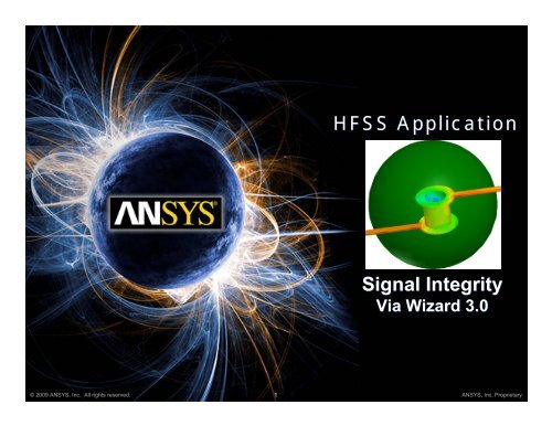
HFSS Application<br />
<strong>Signal</strong> <strong>Integrity</strong><br />
<strong>Via</strong> <strong>Wizard</strong> <strong>3.0</strong><br />
© 2009 ANSYS, Inc. All rights reserved. 1 ANSYS, Inc. Proprietary
<strong>Signal</strong> <strong>Integrity</strong> in HFSS<br />
• <strong>Via</strong>s in Package and PCB Structures<br />
– Differential and Single-ended<br />
• <strong>Via</strong> <strong>Wizard</strong><br />
– Terminal S-parameters<br />
– Setting up differential pairs<br />
– Viewing Results<br />
– Creating Reports<br />
© 2009 ANSYS, Inc. All rights reserved. 2 ANSYS, Inc. Proprietary
<strong>Via</strong>s – Why Simulate Them?<br />
• To stay out of trouble<br />
• <strong>Via</strong>s can cause problems<br />
– Capacitive discontinuity leads to reflections/loss<br />
– Increase crosstalk<br />
– Change return path of the signal<br />
– Excite model cavities leading to EMI<br />
• Properly designed vias limit signal degradation<br />
– Faster data rates<br />
– Lower BER<br />
© 2009 ANSYS, Inc. All rights reserved. 3 ANSYS, Inc. Proprietary
Excuses, Excuses<br />
• 3D simulations are difficult<br />
– Ports and boundaries are confusing<br />
– Tough to draw 3D geometries<br />
• Takes too long to setup<br />
• Takes too long to simulate<br />
• Difficult to parameterize<br />
© 2009 ANSYS, Inc. All rights reserved. 4 ANSYS, Inc. Proprietary
<strong>Via</strong> <strong>Wizard</strong> Overview<br />
• The <strong>Via</strong> <strong>Wizard</strong> creates a ready to solve HFSS project for<br />
an arbitrary stackup and array of vias<br />
• Anybody can use it regardless of CAD experience or<br />
simulation background<br />
• Ports and boundaries automatically setup<br />
• Geometry is fully parameterized and optimization studies<br />
are easy to perform<br />
• Solution settings are optimized based on Ansoft’s best<br />
known methods for speed and accuracy<br />
© 2009 ANSYS, Inc. All rights reserved. 5 ANSYS, Inc. Proprietary
Step 1: Define Stackup<br />
• Add Layers<br />
• Define Materials<br />
– All Dielectric materials are frequency dependent, using a<br />
Djordjevic-Sarkar Model<br />
• Enter Thickness<br />
• Choose Solid or Plane Layer<br />
© 2009 ANSYS, Inc. All rights reserved. 6 ANSYS, Inc. Proprietary
Step 2: Define Padstacks<br />
• Drill Size<br />
• Pads on Layers<br />
• Antipads<br />
© 2009 ANSYS, Inc. All rights reserved. 7 ANSYS, Inc. Proprietary
Step 3: Define <strong>Via</strong> Array<br />
• Select Padstack<br />
• Define Locations<br />
• Port Type<br />
• Connection Layers<br />
• Trace Widths<br />
• SE or Differential<br />
© 2009 ANSYS, Inc. All rights reserved. 8 ANSYS, Inc. Proprietary
Step 4: HFSS Options (optional)<br />
• Set Model Units<br />
• Solve and/or Launch HFSS<br />
• Set Model Options<br />
• Setup Frequency Sweep<br />
© 2009 ANSYS, Inc. All rights reserved. 9 ANSYS, Inc. Proprietary
Generate HFSS Project<br />
• Ready to Solve Project includes<br />
– Boundaries<br />
– Excitations<br />
– Analysis Setup<br />
– Variables<br />
© 2009 ANSYS, Inc. All rights reserved. 10 ANSYS, Inc. Proprietary
Differential Pair Setup<br />
• Right-click on Excitations to Setup Differential Pairs<br />
– Pairs can be created for both Wave Ports and Lump Ports<br />
© 2009 ANSYS, Inc. All rights reserved. 11 ANSYS, Inc. Proprietary
Creating Reports<br />
• Create Reports for Both Differential and Terminal Data<br />
© 2009 ANSYS, Inc. All rights reserved. 12 ANSYS, Inc. Proprietary
Creating Reports<br />
• Create and Display Both SE and DE at the Same Time<br />
© 2009 ANSYS, Inc. All rights reserved. 13 ANSYS, Inc. Proprietary
Viewing Solution Data<br />
• View Modal, Terminal and Differential Pair Data in the<br />
Solutions Window<br />
© 2009 ANSYS, Inc. All rights reserved. 14 ANSYS, Inc. Proprietary
Why Terminal S-parameters?<br />
• Terminal S-Parameters<br />
– By default the S-parameters in HFSS are expressed in terms of<br />
incident and reflected complex amplitudes of waveguide modes<br />
(modal S-parameters)<br />
– In the multi-conductor problems (where multiple modes are<br />
propagating simultaneously) these modes can be converted to<br />
physical quantities directly related to conductors such as currents<br />
• Examples<br />
– Coupled lines on PCBs and Packages<br />
– Multi-pin connectors<br />
– The Terminal S-parameter option was added to HFSS so terminal<br />
currents and voltages could be simulated directly. (Without this<br />
option we would have to determine these combinations<br />
ourselves)<br />
© 2009 ANSYS, Inc. All rights reserved. 15 ANSYS, Inc. Proprietary


