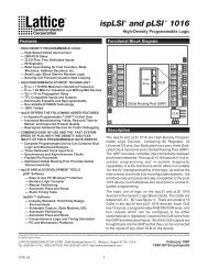
Beginner's Guide to ispLSI and pLSI Using pDS Software
Beginner's Guide to ispLSI and pLSI Using pDS Software
Beginner's Guide to ispLSI and pLSI Using pDS Software

You also want an ePaper? Increase the reach of your titles
YUMPU automatically turns print PDFs into web optimized ePapers that Google loves.
Introduction<br />
This Beginner’s <strong>Guide</strong> is designed <strong>to</strong> familiarize you with<br />
the Lattice <strong>is<strong>pLSI</strong></strong> <strong>and</strong> <strong>pLSI</strong> devices <strong>and</strong> the Lattice <strong>pLSI</strong><br />
<strong>and</strong> <strong>is<strong>pLSI</strong></strong> Development System (<strong>pDS</strong>). To accomplish<br />
this, the complete design of a simple four-bit counter is<br />
discussed from specification through programming <strong>and</strong><br />
testing the part. The following assumptions are made.<br />
First, you have read <strong>and</strong> unders<strong>to</strong>od the <strong>is<strong>pLSI</strong></strong> 1032E<br />
data sheet. Next, you have the documentation for<br />
Microsoft ® Windows readily available. Everything else<br />
is included in the Beginner’s <strong>Guide</strong>.<br />
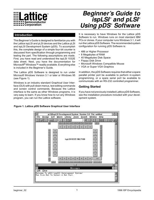
The Lattice <strong>pDS</strong> <strong>Software</strong> is designed <strong>to</strong> run under<br />
Microsoft Windows Version 3.1 or later or Windows 95<br />
(see Figure 1).<br />
Windows is an industry st<strong>and</strong>ard Graphical User Interface<br />
(GUI) with pull-down menus, text editing comm<strong>and</strong>s<br />
<strong>and</strong> screen control comm<strong>and</strong>s. Because the Lattice<br />
interface is the same as other Windows programs, it is<br />
very easy <strong>to</strong> learn. If you know how <strong>to</strong> run any Windows<br />
program, you can run the Lattice software.<br />
Figure 1. Lattice <strong>pDS</strong> <strong>Software</strong> Graphical User Interface<br />
beginner_02<br />
Beginner’s <strong>Guide</strong> <strong>to</strong><br />
®<br />
<strong>is<strong>pLSI</strong></strong> <strong>and</strong> <strong>pLSI</strong>i<br />
®<br />
<strong>Using</strong> <strong>pDS</strong> <strong>Software</strong><br />
It is necessary <strong>to</strong> have Windows for the Lattice <strong>pDS</strong><br />
<strong>Software</strong> <strong>to</strong> run. Windows runs on most st<strong>and</strong>ard IBM<br />
PCs or clones. If your computer runs Windows 3.1, it will<br />
run the Lattice <strong>pDS</strong> <strong>Software</strong>. The recommended system<br />
configuration for running <strong>pDS</strong> <strong>Software</strong> is:<br />
• 486 or Higher Processor<br />
• 8 Megabytes of RAM<br />
• 40 Megabytes Disk Space<br />
• Floppy Disk Drive<br />
• Microsoft Windows Compatible Mouse<br />
• VGA or Super VGA Graphics<br />
In addition, the <strong>pDS</strong> <strong>Software</strong> requires that either a spare<br />
parallel printer port be available <strong>to</strong> perform in-system<br />
programming, or a spare serial port be available <strong>to</strong><br />
communicate with an RS-232 controlled programmer.<br />
Getting Started<br />
If you have not previously installed Lattice <strong>pDS</strong> <strong>Software</strong>,<br />
see the installation procedure included with your development<br />
system.<br />
1 1996 ISP Encyclopedia<br />
®
Beginner’s <strong>Guide</strong> <strong>to</strong> <strong>is<strong>pLSI</strong></strong> <strong>and</strong> <strong>pLSI</strong><br />
<strong>Using</strong> <strong>pDS</strong> <strong>Software</strong><br />
1. Install the Lattice <strong>pDS</strong> <strong>Software</strong> according <strong>to</strong> the<br />
installation instructions. A new program group called<br />
Lattice Semiconduc<strong>to</strong>r is created. This program group<br />
contains icons resembling the Lattice company logo<br />
(see Figure 2).<br />
2. To start the <strong>pDS</strong> <strong>Software</strong>, double click on the Lattice<br />
<strong>pDS</strong> 3.0 logo icon.<br />
Before proceeding, some Microsoft Windows tasks that<br />
you should be able <strong>to</strong> perform include:<br />
• Selecting a menu item using the mouse<br />
• <strong>Using</strong> Open, Save <strong>and</strong> Save As menu items<br />
• Entering comm<strong>and</strong>s <strong>and</strong> text in<strong>to</strong> message windows<br />
<strong>and</strong> dialog boxes<br />
• Moving around the screen using scroll bars<br />
• Editing text using the keyboard <strong>and</strong> mouse <strong>to</strong>:<br />
- Select the insertion point<br />
- Select text by highlighting it<br />
- Cut, paste <strong>and</strong> copy text<br />
If you are unfamiliar with any of these options, take time<br />
<strong>to</strong> go through the Windows Users <strong>Guide</strong>. If you have<br />
worked with an Apple Macin<strong>to</strong>sh, you will find that<br />
many of the comm<strong>and</strong>s <strong>and</strong> operations are similar.<br />
Figure 3. Design Entry Window<br />
Menu Bar<br />
Generic Logic<br />
Blocks<br />
I/O Cells<br />
Dedicated<br />
Input Pins<br />
Message<br />
Window<br />
Figure 2. Lattice Program Group Window<br />
A Brief Tour of the Screen<br />
Once you invoke the Lattice <strong>pDS</strong> <strong>Software</strong>, two windows<br />
are displayed (see Figures 8 <strong>and</strong> 9).<br />
The larger of the two windows displays a graphical<br />
representation of the <strong>is<strong>pLSI</strong></strong> 1032E logic diagram. This<br />
window is called the Data Entry Window. The design is<br />
entered by editing equations in the Data Entry Window.<br />
The smaller of the two windows is the Message Window<br />
<strong>and</strong> it is located at the bot<strong>to</strong>m of the screen. The <strong>pDS</strong><br />
<strong>Software</strong> communicates with you by placing messages<br />
in the message window.<br />
Drop-Down<br />
Menus<br />
Megablock<br />
Clock<br />
Inputs<br />
Scroll Bars<br />
2 1996 ISP Encyclopedia
The part displayed in the block diagram shows the<br />
elements of the <strong>is<strong>pLSI</strong></strong> 1032E that can be modified by the<br />
user. These elements are GLBs, I/O Cells, dedicated<br />
input pins <strong>and</strong> clock input pins, as shown in Figure 3.<br />
The design is entered by clicking the element you wish <strong>to</strong><br />
edit <strong>and</strong> entering equations or macros (library elements<br />
already partitioned <strong>and</strong> optimized for high performance)<br />
in<strong>to</strong> the Edit Windows (see Figure 4).<br />
The method of entering configuration data in<strong>to</strong> a cell<br />
depends on the type of cell:<br />
Configuration data for Generic Logic Blocks is entered<br />
using a combination of Boolean Equations or macros<br />
from the Lattice St<strong>and</strong>ard Library or TTL Library.<br />
Configuration data for I/O Cells is entered using macros<br />
only. There is a complete set of macros which describes<br />
all possible combinations of input, output, <strong>and</strong> I/O cell<br />
configurations.<br />
Configuration data for the Dedicated Input Pins <strong>and</strong> the<br />
Clock Input Pins is entered using a subset of the I/O Cell<br />
macros. Because these pins are inputs only, <strong>and</strong> do not<br />
have input registers, only certain I/O Cell macros apply.<br />
Figure 4. Open Edit Windows<br />
Beginner’s <strong>Guide</strong> <strong>to</strong> <strong>is<strong>pLSI</strong></strong> <strong>and</strong> <strong>pLSI</strong><br />
<strong>Using</strong> <strong>pDS</strong> <strong>Software</strong><br />
The Design Flow<br />
Before starting our sample design, it is valuable <strong>to</strong> underst<strong>and</strong><br />
the Design Flow. The following steps are necessary<br />
<strong>to</strong> complete a design. Refer <strong>to</strong> Figure 5 for more information.<br />
Specifying the Design<br />
A design is specified using one of the two approaches.<br />
With the first method, you use an existing design, consisting<br />
of TTL-like logic elements <strong>and</strong> fit the design in<strong>to</strong> the<br />
<strong>is<strong>pLSI</strong></strong> part. With the second method, you design a circuit<br />
that is optimized for best performance <strong>and</strong> utilization of<br />
the <strong>is<strong>pLSI</strong></strong> architecture.<br />
The first approach consists of simply selecting macros<br />
from the Lattice library that match the functions of the TTL<br />
or CMOS circuits <strong>and</strong> then connecting them <strong>to</strong> each<br />
other. <strong>Using</strong> this approach, a design can be completed<br />
quickly with a high degree of initial success because the<br />
macro circuit elements have been tested.<br />
The second approach ensures better performance <strong>and</strong><br />
higher utilization, but may require some circuit redesign.<br />
Many designs are a combination of the two approaches.<br />
GLB Edit<br />
Windows<br />
I/O Cell<br />
Edit Windows<br />
3 1996 ISP Encyclopedia
Beginner’s <strong>Guide</strong> <strong>to</strong> <strong>is<strong>pLSI</strong></strong> <strong>and</strong> <strong>pLSI</strong><br />
<strong>Using</strong> <strong>pDS</strong> <strong>Software</strong><br />
Figure 5. Design Process Flow<br />
Enter Fixed<br />
Pin Location<br />
Yes<br />
Yes<br />
Start<br />
Specify the Design<br />
Partition the Logic<br />
In<strong>to</strong> GLBs<br />
Enter Equation for the<br />
Single Generic<br />
Logic Blocks<br />
More GLBs<br />
required<br />
?<br />
No<br />
Enter Data for<br />
I/O Cells<br />
Fixed Pin<br />
?<br />
To select the correct <strong>is<strong>pLSI</strong></strong> device, partition the design<br />
in<strong>to</strong> GLBs, <strong>and</strong> count the number of GLBs <strong>and</strong> I/O cells<br />
used. Next, select the <strong>is<strong>pLSI</strong></strong> device that can hold the<br />
amount of logic required. Selection of the proper device<br />
is based on the amount of logic required <strong>and</strong> on the<br />
number of I/O cells needed.<br />
The best utilization <strong>and</strong> routability are achieved by allowing<br />
the software <strong>to</strong> assign I/O pin placement. It is a good<br />
idea <strong>to</strong> design the <strong>is<strong>pLSI</strong></strong> part first, <strong>and</strong> then lay out the<br />
printed circuit board or wire-wrap board. Once the software<br />
intelligently assigns the pin placement the first time,<br />
the pins can be fixed, <strong>and</strong> changes can be made <strong>to</strong> the<br />
logic.<br />
No<br />
Global Verify All<br />
Chip Logic<br />
Verify<br />
?<br />
Route<br />
Yes<br />
Successful<br />
?<br />
Yes<br />
Fuse Map<br />
Program Part<br />
Test Design<br />
End<br />
No<br />
No<br />
Correct Data<br />
<strong>and</strong> Re-verify<br />
Unfix Pins, Remove<br />
Critical Nets, <strong>and</strong><br />
Try Again<br />
0253B<br />
Partitioning the Design<br />
Partitioning consists of dividing the logic in<strong>to</strong> groups that<br />
conveniently fit in<strong>to</strong> the <strong>is<strong>pLSI</strong></strong> Generic Logic Blocks.<br />
These general rules should be followed when partitioning<br />
logic:<br />
• Look at the Macro Library <strong>and</strong> decide if any of the<br />
logic can be implemented using the st<strong>and</strong>ard macros.<br />
Macros are already partitioned <strong>and</strong> are optimized<br />
for high utilization <strong>and</strong> high performance. Macros are<br />
also the fastest method <strong>to</strong> input the logic design.<br />
• Know the capabilities of the GLB. It has 18 inputs <strong>and</strong><br />
four outputs. The GLB has 20 Product Terms (PTs)<br />
that are grouped <strong>to</strong>gether in groups of four, four, five,<br />
<strong>and</strong> seven PTs. The registers in the GLB share a<br />
common clock. The registers within the GLB also<br />
share a common Reset Product Term.<br />
4 1996 ISP Encyclopedia
Figure 6. Counter Schematic Diagram<br />
CI<br />
CE<br />
RESET<br />
CLOCK<br />
Figure 7. Sample Cascadable Counter Logic<br />
Beginner’s <strong>Guide</strong> <strong>to</strong> <strong>is<strong>pLSI</strong></strong> <strong>and</strong> <strong>pLSI</strong><br />
<strong>Using</strong> <strong>pDS</strong> <strong>Software</strong><br />
D Q<br />
D Q<br />
D Q<br />
D Q<br />
Q0<br />
Q1<br />
Q2<br />
Q3<br />
CO<br />
I/O 0 Carry In Carry Out I/O 32<br />
I/O 1<br />
Y0<br />
I/O 2<br />
Count<br />
Enable<br />
Clock<br />
Reset<br />
• When an output has been fixed <strong>to</strong> a specific I/O pin,<br />
the signal that is used <strong>to</strong> generate that output must be<br />
generated within the same Megablock.<br />
• There is only one Output Enable signal per Megablock.<br />
Outputs which share a common Output Enable<br />
signal should be placed in the same Megablock (see<br />
Figure 3).<br />
4-bit Binary<br />
Cascadable<br />
Counter<br />
Q0 Q1 Q2 Q3<br />
I/O 36<br />
I/O 37<br />
I/O 38<br />
I/O 39<br />
• Signals that are related <strong>to</strong> each other, such as those<br />
used for counters, shift registers, etc., should be<br />
placed in<strong>to</strong> the same Megablock. This is done <strong>to</strong><br />
reduce routing congestion.<br />
Compiling the Design<br />
Compiling the design is done using the Lattice <strong>pDS</strong><br />
<strong>Software</strong> <strong>and</strong> consists of four steps:<br />
5 1996 ISP Encyclopedia
Beginner’s <strong>Guide</strong> <strong>to</strong> <strong>is<strong>pLSI</strong></strong> <strong>and</strong> <strong>pLSI</strong><br />
<strong>Using</strong> <strong>pDS</strong> <strong>Software</strong><br />
1. Entering the design. Boolean equations or macros<br />
are entered in<strong>to</strong> the various cells <strong>and</strong> blocks on the<br />
<strong>is<strong>pLSI</strong></strong> device using a built in text edi<strong>to</strong>r. After each<br />
cell has been entered, a Local Verify is done <strong>to</strong> check<br />
for syntax or logic errors within that cell.<br />
2. Verifying the design. This is done globally after all<br />
the design has been entered. This verification looks<br />
for such problems as inputs that are not connected <strong>to</strong><br />
the GLBs or nets that have duplicate names. The<br />
design must completely pass a Global Verify before<br />
any of the following steps can happen.<br />
3. Routing the design. This is the next step after a<br />
successful Verify. The Router interconnects the Generic<br />
Logic Block <strong>and</strong> I/O Cell inputs <strong>and</strong> outputs. The<br />
option of fixing certain input <strong>and</strong> output signals <strong>to</strong><br />
specific device pins is now available.<br />
4. Generating the Fusemap. This takes the verified<br />
<strong>and</strong> routed design <strong>and</strong> creates the JEDEC file (a<br />
st<strong>and</strong>ard binary fuse file) necessary <strong>to</strong> program the<br />
part. This is a modified format JEDEC file with a suffix<br />
of .JED.<br />
Programming the Part<br />
Once the design has been compiled, the next step is <strong>to</strong><br />
program the part. This can either be done on the board<br />
if using in-system programming (ISP) or in a separate<br />
programmer. <strong>Using</strong> a separate programmer requires<br />
that the part be removed from the target system socket<br />
<strong>and</strong> inserted in<strong>to</strong> a programmer.<br />
Testing the Design<br />
The last step in the process is testing the design. The<br />
design is tested by putting it on the board <strong>and</strong> seeing if it<br />
works correctly. If corrections need <strong>to</strong> be made, the<br />
appropriate GLBs or I/O Cells are reprogrammed, <strong>and</strong><br />
the design is recompiled. Because the <strong>is<strong>pLSI</strong></strong> 1032E is<br />
an electrically erasable <strong>and</strong> reprogrammable part, the<br />
same part can be used again <strong>and</strong> again.<br />
The Sample Design<br />
Listing 1. Counter Equations<br />
Q0 = (Q0 & !_RST) $$ (CI & CE & !_RST)<br />
Q1 = (Q1 & !_RST) $$ (Q0 & CI & CE & !_RST)<br />
Q2 = (Q2 & !_RST) $$ (Q0 & Q1 & CI & CE & !_RST)<br />
Q3 = (Q3 & !_RST) $$ (Q0 & Q1 & Q2 & CI & CE & !_RST)<br />
CO = Q0 & Q1 & Q2 & Q3 & CI & CE<br />
Listing 2. GLB Equations<br />
The sample design is a simple one. We are going <strong>to</strong><br />
design a 4-bit binary counter using Boolean equations<br />
<strong>and</strong> place it in<strong>to</strong> an <strong>is<strong>pLSI</strong></strong> 1032E device. We will then<br />
take the design through the compilation process, generate<br />
a fuse file <strong>and</strong> program a part.<br />
The counter has the following specifications:<br />
SIGTYPE Q0 REG OUT;<br />
SIGTYPE Q1 REG OUT;<br />
SIGTYPE Q2 REG OUT;<br />
SIGTYPE Q3 REG OUT;<br />
EQUATIONS<br />
Q0.CLK = _CLK;<br />
Q0 = (Q0 & !_RST) $$ (CI & CE & !_RST);<br />
Q1 = (Q1 & !_RST) $$ (Q0 & CI & CE & !_RST);<br />
Q2 = (Q2 & !_RST) $$ (Q0 & Q1 & CI & CE & !_RST);<br />
Q3 = (Q3 & !_RST) $$ (Q0 & Q1 & Q2 & CI & CE & !_RST);<br />
END<br />
• A 4-bit Synchronous Binary Counter.<br />
• Active High Cascade In (CI) <strong>and</strong> Cascade Out<br />
(CO) Pins.<br />
• An Active High Count Enable (CE) Pin.<br />
• A Synchronous Reset Pin.<br />
Figure 6 shows the schematic diagram <strong>and</strong> Figure 7<br />
shows the logic symbol for this counter. Because the<br />
counter has 5 outputs (Q0, Q1, Q2, Q3, <strong>and</strong> Cascade<br />
Out) it occupies two GLBs.<br />
6 1996 ISP Encyclopedia
In this design example, the Clock <strong>and</strong> I/O pins are<br />
assigned <strong>to</strong> be compatible with the Lattice <strong>is<strong>pLSI</strong></strong> 1032E<br />
for a specific printed circuit board. This allows the design<br />
<strong>to</strong> be tested easily.<br />
The input signals Cascade In, Count Enable <strong>and</strong> Reset are<br />
connected <strong>to</strong> three bits of the 8-bit DIP switch, <strong>and</strong> the five<br />
outputs are connected <strong>to</strong> five of the discrete LED outputs.<br />
Defining the Counter<br />
In defining the counter, the first step is <strong>to</strong> write the equations.<br />
The equations for the 4-bit binary counter are expressed in<br />
Listing 1.<br />
There are two inputs <strong>to</strong> the Exclusive-OR gate in front of the<br />
D input <strong>to</strong> the register. We shall call the one that receives its<br />
input from the feedback of the same register as the data<br />
input. It is <strong>to</strong> the left of the $$ (XOR) symbol in the above<br />
equations. The other input is connected <strong>to</strong> the control terms<br />
Cascade In <strong>and</strong> Count Enable. These are called the control<br />
input. When the control input <strong>to</strong> the XOR is a zero the output<br />
of the XOR follows the data input (Hold.) When the control<br />
Input is a one, the output of the XOR is inverted from the<br />
input (Increment.)<br />
Figure 8. Examples of Cell Entry Windows with Equations<br />
Beginner’s <strong>Guide</strong> <strong>to</strong> <strong>is<strong>pLSI</strong></strong> <strong>and</strong> <strong>pLSI</strong><br />
<strong>Using</strong> <strong>pDS</strong> <strong>Software</strong><br />
When either Cascade In or Count Enable is low <strong>and</strong> RST<br />
is low, the Q0 output from the counter remains in its<br />
current state (Hold). When Cascade In <strong>and</strong> Count Enable<br />
are both high <strong>and</strong> RST is low, the Q0 output <strong>to</strong>ggles on<br />
each successive clock (Increment.) When RST goes<br />
high, the inputs <strong>to</strong> the data side of the XOR gate <strong>and</strong> the<br />
control side go low. This causes the output of the counter<br />
<strong>to</strong> go low on the next clock edge (Reset.)<br />
Each successive stage operates similarly, except during<br />
transition, (Increment), when the outputs of all previous<br />
stages are at Logic Level One. The Carry Out signal is<br />
only generated when all the stages have reached a one<br />
<strong>and</strong> both Cascade In <strong>and</strong> Counter Enable are a one.<br />
Once the equations have been defined, enter them in<strong>to</strong><br />
the GLBs. Follow these steps:<br />
1. From within Windows, start the Lattice <strong>pDS</strong> <strong>Software</strong><br />
by double clicking on the Lattice Icon.<br />
2. When the Lattice software starts, it displays the block<br />
diagram of the <strong>is<strong>pLSI</strong></strong> 1032E part. Open GLB C1 for<br />
editing by double clicking on it. The edit window<br />
displays.<br />
7 1996 ISP Encyclopedia
Beginner’s <strong>Guide</strong> <strong>to</strong> <strong>is<strong>pLSI</strong></strong> <strong>and</strong> <strong>pLSI</strong><br />
<strong>Using</strong> <strong>pDS</strong> <strong>Software</strong><br />
3. Enter the equations shown in Listing 2 in<strong>to</strong> the edit<br />
window for GLB C1.<br />
4. Verify the equations by clicking on the Cell Verify<br />
menu option. If errors appear in the Message window,<br />
find out what is wrong, <strong>and</strong> correct it. Things <strong>to</strong><br />
look for are typing errors, missing semicolons, or<br />
incorrect symbols. Re-verify after making corrections.<br />
5. Close the Edit window for GLB C1 by selecting the<br />
Done option from the Cell Edit Menu.<br />
6. Open GLB C2 for editing by double clicking on it.<br />
7. Enter the following equations in<strong>to</strong> the edit window for<br />
GLB C2:<br />
SIGTYPE CO OUT;<br />
EQUATIONS<br />
CO = Q0 & Q1 & Q2 & Q3 & CI & CE;<br />
END<br />
8. Verify the equations by clicking on the Cell Verify<br />
menu option.<br />
9. Close the Cell Edit window by clicking on the Done<br />
option in the menu bar.<br />
At this point, the logic for the counter is completely<br />
specified, but we still must connect the Clock <strong>and</strong> the<br />
Inputs <strong>and</strong> Outputs.<br />
10. Open Clock Input Y0 by double clicking on it. It<br />
may be necessary <strong>to</strong> Zoom in on the Clock area of<br />
the Logic Diagram <strong>to</strong> determine which pin is Y0.<br />
11. Enter the following equations in<strong>to</strong> the edit window<br />
for Clock Input Y0:<br />
XPIN CLK X_CLK LOCK 20;<br />
IB11 (_CLK, X_CLK );<br />
12. Verify the equations by clicking on the Cell Verify<br />
menu option.<br />
13. Once the cell verifies correctly, close the Cell Edit<br />
window by clicking on the Done option in the menu<br />
bar.<br />
14. Repeat Steps 10 through 13 for the Cascade In<br />
input pin located at I/O 0 using these equations:<br />
XPIN IO XCI LOCK 26;<br />
IB11 (CI, XCI);<br />
15. Repeat Steps 10 through 13 for the Count Enable<br />
input pin located at I/O 1 using these equations:<br />
XPIN IO XCE LOCK 27;<br />
IB11 (CE, XCE);<br />
16. Repeat Steps 10 through 13 for the Reset input pin<br />
located at I/O 2 using these equations:<br />
XPIN IO X_RST LOCK 28;<br />
IB11 (_RST, X_RST);<br />
17. Repeat Steps 10 through 13 for the Q0 output pin<br />
located at I/O 39 using these equations:<br />
XPIN IO XQ0 LOCK 75;<br />
OB11 (XQ0, Q0);<br />
18. Repeat Steps 10 through 13 for the Q1 output pin<br />
located at I/O 38 using these equations:<br />
XPIN IO XQ1 LOCK 74;<br />
OB11 (XQ1, Q1);<br />
Note: With the Lattice <strong>pDS</strong> <strong>Software</strong> you can have<br />
multiple Edit Windows open at the same time. This<br />
means that you can Copy the equations from I/O Cell 39<br />
<strong>and</strong> Paste them in<strong>to</strong> I/O Cell 38. The data in both cells is<br />
similar, <strong>and</strong> you can use the Windows editing comm<strong>and</strong>s<br />
<strong>to</strong> make changes.<br />
19. Repeat Steps 10 through 13 for the Q2 output pin<br />
located at I/O 37 using these equations:<br />
XPIN IO XQ2 LOCK 73;<br />
OB11 (XQ2, Q2);<br />
20. Repeat Steps 10 through 13 for the Q3 output pin<br />
located at I/O 36 using these equations:<br />
XPIN IO XQ3 LOCK 72;<br />
OB11 (XQ3, Q3);<br />
21. Repeat Steps 10 through 13 for the Carry Out output<br />
pin located at I/O 35 using these equations:<br />
XPIN IO XCO LOCK 71;<br />
OB11 (XCO, CO);<br />
Now, the Inputs, Outputs <strong>and</strong> Clocks are connected,<br />
<strong>and</strong> the equations for the counter have been entered<br />
<strong>and</strong> verified. The design is complete <strong>and</strong> ready <strong>to</strong> be<br />
Globally Verified. Before proceeding, save your work.<br />
22. From the Menu Bar, select the File Option, <strong>and</strong><br />
choose Save As. The <strong>pDS</strong> <strong>Software</strong> prompts you for<br />
the file name. Type in the name COUNTER. The<br />
suffix .LIF (Lattice Internal File) is au<strong>to</strong>matically appended.<br />
8 1996 ISP Encyclopedia
Review of the Syntax<br />
This is a brief review of the syntax used in the example<br />
design. For complete information see the Language<br />
Reference section of the <strong>Software</strong> Manual included<br />
with the Lattice <strong>pDS</strong> <strong>Software</strong>.<br />
The opera<strong>to</strong>rs that the Lattice <strong>pDS</strong> <strong>Software</strong> uses are similar<br />
<strong>to</strong> those used by the Data I/O ABEL program. The<br />
opera<strong>to</strong>rs <strong>and</strong> an example of how they are used are shown<br />
in the table below. The Precedence of Evaluation is also<br />
shown where 1 is the highest precedence (see table below).<br />
Table: Precedence of Evaluation<br />
Opera<strong>to</strong>r Precedence Description Example<br />
!<br />
$$<br />
&<br />
#<br />
$<br />
!$<br />
1<br />
2<br />
3<br />
4<br />
5<br />
5<br />
NOT<br />
XOR (XOR<br />
Gate in GLB<br />
AND<br />
OR<br />
XOR (Soft)<br />
XNOR (Soft)<br />
In addition <strong>to</strong> the equations, there are several other<br />
lines that need <strong>to</strong> be included in the GLB or I/O Cell<br />
definition. They are:<br />
SYM; The symbol line consists of five parts:<br />
- The Keyword SYM that indicates<br />
what type of line this is <strong>to</strong> be.<br />
Programming the Device<br />
Beginner’s <strong>Guide</strong> <strong>to</strong> <strong>is<strong>pLSI</strong></strong> <strong>and</strong> <strong>pLSI</strong><br />
<strong>Using</strong> <strong>pDS</strong> <strong>Software</strong><br />
!A<br />
A $$ B<br />
A & B<br />
A # B<br />
A $ B<br />
A !$ B<br />
The Fuse map program generated a fuse (.JED) file<br />
which needs <strong>to</strong> be permanently programmed in<strong>to</strong> an<br />
<strong>is<strong>pLSI</strong></strong> or <strong>pLSI</strong> 1032E device. Programming the part is<br />
done using one of three methods:<br />
• In-system program for <strong>is<strong>pLSI</strong></strong> device<br />
• Motherboard Programmer for <strong>is<strong>pLSI</strong></strong> device<br />
• RS-232 Link Programmer for <strong>is<strong>pLSI</strong></strong> or <strong>pLSI</strong> device<br />
An ispDOWNLOAD Cable is provided with <strong>pDS</strong> <strong>Software</strong><br />
. The cable connects <strong>to</strong> the parallel port on a PC <strong>and</strong><br />
controls the programming process. If the target system is<br />
designed <strong>to</strong> use in-system programming, the part can be<br />
- The Symbol Name. This is either<br />
GLB or IOC.<br />
- The Cell location.<br />
- The Symbol Level used by other software<br />
packages. For our purposes,<br />
always use a 1.<br />
- The Symbol User Name. This is an<br />
assigned name that appears in the<br />
GLB or IOC in place of its location<br />
designation.<br />
SIGTYPE; Used <strong>to</strong> define signal attributes within a<br />
GLB.<br />
OUT defines a combina<strong>to</strong>rial output.<br />
REG OUT defines a Registered<br />
Output.<br />
EQUATIONS; Indicate the start of the Equation Section<br />
for a GLB or I/O Cell.<br />
MACRO; Indicates the usage of a Macro Logic<br />
Element from the Macro Library.<br />
END; Signifies the end of an Equation Section,<br />
a GLB or I/O Cell definition,<br />
a Declaration Section, or a Macro Definition.<br />
There can be more than one<br />
END statement in a GLB.<br />
Comments are indicated by preceding the comment<br />
with two forward slashes:<br />
// This is an example comment line.<br />
programmed right on the board or using the isp Engineering<br />
Kit.<br />
For designers who need <strong>to</strong> integrate ISP in<strong>to</strong> their onboard<br />
programming control using a microprocessor, Lattice<br />
provides ispCODE (C source code) <strong>to</strong> allow for<br />
cus<strong>to</strong>mization of the ISP user interface.<br />
For a programmer controlled by a serial RS-232 link, the<br />
Lattice <strong>pDS</strong> <strong>Software</strong> can call up the Windows Terminal<br />
Program. By using your PC <strong>to</strong> emulate a terminal, you<br />
can give the programmer the comm<strong>and</strong>s necessary <strong>to</strong><br />
set it up <strong>to</strong> receive the .JED file. The Download comm<strong>and</strong><br />
in the Windows Terminal program transfers the file <strong>to</strong> the<br />
programmer. Because the .JED file is an ASCII format, a<br />
text download is used.<br />
9 1996 ISP Encyclopedia
Beginner’s <strong>Guide</strong> <strong>to</strong> <strong>is<strong>pLSI</strong></strong> <strong>and</strong> <strong>pLSI</strong><br />
<strong>Using</strong> <strong>pDS</strong> <strong>Software</strong><br />
For programming the <strong>is<strong>pLSI</strong></strong> 1032E part, follow these<br />
comm<strong>and</strong>s.<br />
1. From the Design Menu select the Program Option.<br />
This invokes the In-system Programming module.<br />
2. The ISP module prompts for the name of the JEDEC<br />
file. Click on COUNTER.JED in the file list <strong>and</strong> then<br />
click OK. It may already have COUNTER.JED as the<br />
default file name. If so, click OK.<br />
3. Programming takes a few seconds. If any errors<br />
are encountered, they are listed in the message<br />
box.<br />
When programming is complete, the part is reset <strong>and</strong> sent<br />
back in<strong>to</strong> operating mode. It can then be tested by applying<br />
the required inputs <strong>and</strong> reviewing the outputs.<br />
Advanced Design Concepts<br />
Working with Macros<br />
The Lattice <strong>pDS</strong> <strong>Software</strong> comes with a library of over 200<br />
macro logic elements. These logic blocks are similar <strong>to</strong><br />
7400 TTL logic. Some example macros are listed in Table<br />
1.<br />
For complete information on the Macro or TTL Libraries,<br />
refer <strong>to</strong> the Macro Reference Manual <strong>and</strong> TTL Reference<br />
that come with the Lattice <strong>pDS</strong> <strong>Software</strong>. In addition <strong>to</strong><br />
using macros from the Lattice libraries, you can create<br />
cus<strong>to</strong>m macros from scratch or modify macros from the<br />
Lattice library <strong>to</strong> satisfy design requirements.<br />
We are going <strong>to</strong> take a macro from the library that is identical<br />
<strong>to</strong> the counter just created, <strong>and</strong> cascade it with the counter.<br />
Table 1. Macro Logic Element Examples<br />
The macro element used <strong>to</strong> do this is named CBU24. The<br />
schematic diagram is shown in Figure 9.<br />
1. Read in the previous design using the File Open<br />
comm<strong>and</strong>. The name of the file is COUNTER.LIF.<br />
2. Choose the Library menu option <strong>and</strong> highlight Select<br />
<strong>to</strong> invoke the library window. Click on the System Lib<br />
but<strong>to</strong>n <strong>and</strong> then click OK.<br />
3. Invoke the Macro Window by clicking on MACRO in<br />
the Menu Bar.<br />
4. Select the macro CBU24 from the list of macros.<br />
5. Click on GLB C3 <strong>to</strong> select it.<br />
6. Click on the PLACE comm<strong>and</strong> in the Macro Menu.<br />
This places the first half of the four-bit counter macro<br />
in GLB C3. The signal names placed in the GLB are<br />
the default signal names, <strong>and</strong> need <strong>to</strong> be changed <strong>to</strong><br />
correspond <strong>to</strong> the signal names so that the router is<br />
able <strong>to</strong> connect them.<br />
7. The original text in the cell was:<br />
CBU24_2(CAO,[Q0..Q3],CAI,EN);<br />
Change that <strong>to</strong> read:<br />
CBU24_2(CAO,[Q4..Q7],CO,CE);<br />
The default signal names are changed <strong>to</strong> match those<br />
already used in as shown in Table 2.<br />
8. Perform a Cell Verify <strong>to</strong> ensure that no errors were<br />
introduced.<br />
9. Click on DONE <strong>to</strong> close that GLB.<br />
Macro Name 7400 Part Description Number of<br />
Equivalent GLBs Used<br />
AND2<br />
XOR2<br />
FJK21<br />
CBU34<br />
BIN27<br />
SRR38<br />
ADDF4<br />
7408<br />
7486<br />
74112<br />
74161<br />
74247<br />
74166<br />
74283<br />
2 Input AND Gate<br />
2 Input Exclusive OR Gate<br />
J-K Flip-Flop with Asynchronous Clear<br />
4-Bit Preloadable Binary Counter with Reset<br />
BCD <strong>to</strong> 7 Segment Decoder<br />
8-Bit Parallel In-Serial Out Shift Register<br />
4-Bit Full Adder with Look Ahead Carry<br />
1/4<br />
1/4<br />
1/4<br />
1 1/4<br />
2<br />
2<br />
4 3/4<br />
Table 8- 0002<br />
10 1996 ISP Encyclopedia
Beginner’s <strong>Guide</strong> <strong>to</strong> <strong>is<strong>pLSI</strong></strong> <strong>and</strong> <strong>pLSI</strong><br />
<strong>Using</strong> <strong>pDS</strong> <strong>Software</strong><br />
Figure 9. Cus<strong>to</strong>m Binary Counter Cascaded with a St<strong>and</strong>ard Macro Counter<br />
Table 2. Default Signal Names<br />
Default Signal Is<br />
Notes<br />
CAO<br />
Q0..Q3<br />
CAI<br />
EN<br />
I/O 0 Carry In Carry Out<br />
Carry In Carry Out I/O 32<br />
I/O 1<br />
Y0<br />
I/O 2<br />
Cascade Out<br />
Counter Outputs<br />
Cascade In<br />
Enable<br />
Count<br />
Enable<br />
Clock<br />
Reset<br />
Cus<strong>to</strong>m<br />
4-bit Binary<br />
Cascadable<br />
Counter<br />
Q0 Q1 Q2 Q3<br />
CAO<br />
Q4..Q7<br />
CO<br />
CE<br />
10. The macro occupies two GLBs, so the second half of<br />
the macro now needs <strong>to</strong> be placed. Click on GLB C4<br />
<strong>to</strong> place the second half.<br />
11. As before, the signal names that were placed in the<br />
GLB were the default names. They also need <strong>to</strong> be<br />
edited. The Lattice software placed the following<br />
code in<strong>to</strong> the cell:<br />
CBU24_1([Q0..Q3],CAI,CLK,EN,CD);<br />
Change it <strong>to</strong> read:<br />
CBU24_1([Q4..Q7],CO,_CLK,CE,RST);<br />
As before, we have changed the default signal names<br />
<strong>to</strong> match those that we are already using. See Table<br />
3.<br />
Count<br />
Enable<br />
Clock<br />
Reset<br />
Macro CBU24<br />
4-bit Binary<br />
Cascadable<br />
Counter<br />
Q0 Q1 Q2 Q3<br />
I/O 36<br />
I/O 37<br />
I/O 38<br />
I/O 39<br />
I/O 40<br />
I/O 41<br />
I/O 42<br />
I/O 43<br />
This is a new signal. We can use the default name.<br />
We used Q0 through Q3 in the first counter. We need <strong>to</strong><br />
assign new names so the router will not get confused.<br />
CO is the name that we assigned <strong>to</strong> the Cascade Out pin<br />
on the counter that we designed.<br />
We called our Enable pin CE (Count Enable). This comes<br />
from a pin external <strong>to</strong> the device.<br />
12. As before, perform a CELL VERIFY, <strong>and</strong> click on<br />
DONE when finished.<br />
The counter has now been placed, <strong>and</strong> the inputs<br />
connected, but the outputs are still floating. Connect<br />
them <strong>to</strong> the I/O cells as you did with the previous<br />
counter.<br />
13. Select the macro called OB11 from the macro list.<br />
14. Click on IO Cell #40 <strong>to</strong> select it.<br />
15. Click on PLACE in the Macro Window. This configures<br />
I/O Cell #40 as an output buffer, but it used the<br />
default signal names. The text placed in the cell was:<br />
OB11 (XO0,A0);<br />
11 1996 ISP Encyclopedia
Beginner’s <strong>Guide</strong> <strong>to</strong> <strong>is<strong>pLSI</strong></strong> <strong>and</strong> <strong>pLSI</strong><br />
<strong>Using</strong> <strong>pDS</strong> <strong>Software</strong><br />
Table 3. Renaming Default Signal Names<br />
Default Signal Is<br />
Notes<br />
Q0..Q3<br />
CAI<br />
CLK<br />
EN<br />
CD<br />
You should change it <strong>to</strong> read:<br />
OB11 (XO4,Q4);<br />
Q4 is the name of the first output of the counter. XO0<br />
was changed <strong>to</strong> XO4 so there would not be duplicate<br />
I/O cell names when we place the next cells.<br />
15. Click on IO Cell #41 <strong>to</strong> select it.<br />
16. Click on PLACE in the Macro Window. Change the<br />
default signal names <strong>to</strong> match those used in your<br />
design:<br />
OB11 (XO0,A0);<br />
Becomes:<br />
OB11 (XO5,Q5);<br />
Counter Outputs<br />
Cascade In<br />
Clock<br />
Enable<br />
Clear Direct<br />
Q4..Q7<br />
CO<br />
_CLK<br />
CE<br />
RST<br />
17. Use the same technique <strong>to</strong> connect I/O cell #42 <strong>to</strong><br />
counter output Q6.<br />
18. Use the same technique <strong>to</strong> connect I/O cell #43 <strong>to</strong><br />
counter output Q7.<br />
All the outputs are now connected, <strong>and</strong> the design is<br />
complete. As in the first design, you now need <strong>to</strong> do a<br />
Global Verify on the design, Route the nets <strong>and</strong> generate<br />
the Fuse map. You can see from this exercise how<br />
simple it is <strong>to</strong> complete a design using macros.<br />
The use of macros is not limited <strong>to</strong> those in the Lattice<br />
Macro Libraries. Sometimes the st<strong>and</strong>ard macro is close<br />
<strong>to</strong>, but not exactly what you need. You can copy any of<br />
We used Q0 through Q3 in the first counter. We need <strong>to</strong><br />
assign new names so the router will not get confused.<br />
CO is the name that we assigned <strong>to</strong> the Cascade Out pin<br />
on the counter that we designed.<br />
We named the signal that we brought in on pin Y0 _CLK<br />
We called our Enable pin CE (Count Enable). This comes.<br />
in from pin 27.<br />
Our reset signal was brought in on pin 28 <strong>and</strong> called RST.<br />
the st<strong>and</strong>ard Lattice soft macros in<strong>to</strong> a personal library<br />
<strong>and</strong> modify them <strong>to</strong> meet specific needs. You can also<br />
create macros using Boolean equations <strong>and</strong> save them<br />
in your personal library for future use.<br />
Summary<br />
This application note describes how <strong>to</strong> design using <strong>pDS</strong><br />
<strong>Software</strong> from definition <strong>to</strong> completion. In this Beginner’s<br />
<strong>Guide</strong>, we:<br />
• Looked at Lattice <strong>pDS</strong> <strong>Software</strong> <strong>and</strong> its various<br />
elements.<br />
• Explained the design flow from beginning <strong>to</strong> end.<br />
• Looked at the syntax needed for entering a design.<br />
• Defined a small counter <strong>and</strong> partitioned it in<strong>to</strong><br />
GLBs.<br />
• Entered the counter design in<strong>to</strong> the development<br />
system.<br />
• Took the design through the compilation process.<br />
(Verify, Route, <strong>and</strong> Fusemap).<br />
• Programmed a part.<br />
• Tested the design.<br />
• Changed the design <strong>and</strong> introduced the use of<br />
macros.<br />
• Recompiled the design <strong>and</strong> tested it.<br />
If you have followed this procedure, you are ready <strong>to</strong><br />
complete a design of your own.<br />
12 1996 ISP Encyclopedia
Copyright © 1996 Lattice Semiconduc<strong>to</strong>r Corporation.<br />
E 2 CMOS, GAL, ispGAL, <strong>is<strong>pLSI</strong></strong>, <strong>pLSI</strong>, <strong>pDS</strong>, Silicon Forest, UltraMOS, Lattice Logo, L with Lattice Semiconduc<strong>to</strong>r Corp. <strong>and</strong> L<br />
(Stylized) are registered trademarks of Lattice Semiconduc<strong>to</strong>r Corporation (LSC). The LSC Logo, Generic Array Logic, In-<br />
System Programmability, In-System Programmable, ISP, ispATE, ispCODE, ispDOWNLOAD, ispGDS, ispStarter,<br />
ispSTREAM, ispTEST, ispTURBO, Latch-Lock, <strong>pDS</strong>+, RFT, Total ISP <strong>and</strong> Twin GLB are trademarks of Lattice Semiconduc<strong>to</strong>r<br />
Corporation. ISP is a service mark of Lattice Semiconduc<strong>to</strong>r Corporation. All br<strong>and</strong> names or product names mentioned are<br />
trademarks or registered trademarks of their respective holders.<br />
Lattice Semiconduc<strong>to</strong>r Corporation (LSC) products are made under one or more of the following U.S. <strong>and</strong> international<br />
patents: 4,761,768 US, 4,766,569 US, 4,833,646 US, 4,852,044 US, 4,855,954 US, 4,879,688 US, 4,887,239 US, 4,896,296<br />
US, 5,130,574 US, 5,138,198 US, 5,162,679 US, 5,191,243 US, 5,204,556 US, 5,231,315 US, 5,231,316 US, 5,237,218 US,<br />
5,245,226 US, 5,251,169 US, 5,272,666 US, 5,281,906 US, 5,295,095 US, 5,329,179 US, 5,331,590 US, 5,336,951 US,<br />
5,353,246 US, 5,357,156 US, 5,359,573 US, 5,394,033 US, 5,394,037 US, 5,404,055 US, 5,418,390 US, 5,493,205 US,<br />
0194091 EP, 0196771B1 EP, 0267271 EP, 0196771 UK, 0194091 GB, 0196771 WG, P3686070.0-08 WG. LSC does not<br />
represent that products described herein are free from patent infringement or from any third-party right.<br />
The specifications <strong>and</strong> information herein are subject <strong>to</strong> change without notice. Lattice Semiconduc<strong>to</strong>r Corporation (LSC)<br />
reserves the right <strong>to</strong> discontinue any product or service without notice <strong>and</strong> assumes no obligation <strong>to</strong> correct any errors<br />
contained herein or <strong>to</strong> advise any user of this document of any correction if such be made. LSC recommends its cus<strong>to</strong>mers<br />
obtain the latest version of the relevant information <strong>to</strong> establish, before ordering, that the information being relied upon is<br />
current.<br />
LSC warrants performance of its products <strong>to</strong> current <strong>and</strong> applicable specifications in accordance with LSC’s st<strong>and</strong>ard<br />
warranty. Testing <strong>and</strong> other quality control procedures are performed <strong>to</strong> the extent LSC deems necessary. Specific testing of<br />
all parameters of each product is not necessarily performed, unless m<strong>and</strong>ated by government requirements.<br />
LSC assumes no liability for applications assistance, cus<strong>to</strong>mer’s product design, software performance, or infringements of<br />
patents or services arising from the use of the products <strong>and</strong> services described herein.<br />
LSC products are not authorized for use in life-support applications, devices or systems. Inclusion of LSC products in such<br />
applications is prohibited.<br />
LATTICE SEMICONDUCTOR CORPORATION<br />
5555 Northeast Moore Court<br />
Hillsboro, Oregon 97124 U.S.A.<br />
Tel.: (503) 681-0118<br />
FAX: (503) 681-3037<br />
http://www.latticesemi.com November 1996