Introduction to silicon detectors and radiation ... - IRTG Heidelberg
Introduction to silicon detectors and radiation ... - IRTG Heidelberg
Introduction to silicon detectors and radiation ... - IRTG Heidelberg

Create successful ePaper yourself
Turn your PDF publications into a flip-book with our unique Google optimized e-Paper software.
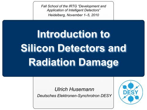
Fall School of the <strong>IRTG</strong> “Development <strong>and</strong><br />
Application of Intelligent Detec<strong>to</strong>rs”<br />
<strong>Heidelberg</strong>, November 1–5, 2010<br />
<strong>Introduction</strong> <strong>to</strong><br />
Silicon Detec<strong>to</strong>rs <strong>and</strong><br />
Radiation Damage<br />
Ulrich Husemann<br />
Deutsches Elektronen-Synchrotron DESY
<strong>Introduction</strong><br />
Introduc<strong>to</strong>ry Lectures: Outline<br />
How <strong>and</strong> where are <strong>silicon</strong> detec<strong>to</strong>rs employed at hadron colliders?<br />
Which detec<strong>to</strong>r components suffer from <strong>radiation</strong> damage?<br />
Part I: Radiation Damage in Silicon Sensors (UH)<br />
What are typical sensor defects caused by <strong>radiation</strong>?<br />
Which operational parameters are affected?<br />
How can <strong>radiation</strong> damage be measured in the lab <strong>and</strong> how can it be modeled?<br />
Part II: Radiation Damage in Silicon Readout Electronics (Ketil Røed)<br />
What is <strong>radiation</strong> environment responsible for inducing single event upsets (SEUs)<br />
in FPGAs?<br />
How do SEUs affect SRAM memory cells <strong>and</strong> FPGAs?<br />
How can SEU failures be tested, predicted, <strong>and</strong> reduced?<br />
<strong>IRTG</strong> Fall School 2010, <strong>Heidelberg</strong>, November 1–5, 2010, U. Husemann: <strong>Introduction</strong> (Part I)<br />
2
<strong>Introduction</strong>
Hadron Collider Experiments<br />
Silicon detec<strong>to</strong>rs employed in<br />
many particle physics experiments<br />
Fixed target<br />
Hadron colliders<br />
Lep<strong>to</strong>n <strong>and</strong> ep colliders,<br />
… <strong>and</strong> for various purposes<br />
Charged particle tracking & vertexing<br />
Calorimetry<br />
This lecture: restricted <strong>to</strong> <strong>silicon</strong>based<br />
tracking <strong>and</strong> vertexing<br />
detec<strong>to</strong>rs at hadron colliders, e.g.<br />
SppS: pp at √s = 630 GeV<br />
Tevatron: pp at √s = 1.8–1.96 TeV<br />
LHC: pp at √s = 7–14 TeV<br />
Fermi National Accelera<strong>to</strong>r Labora<strong>to</strong>ry – Aerial View<br />
LHC<br />
ALICE<br />
<strong>IRTG</strong> Fall School 2010, <strong>Heidelberg</strong>, November 1–5, 2010, U. Husemann: <strong>Introduction</strong> (Part I)<br />
Tevatron<br />
2 km<br />
[Fermilab Visual Media Service]<br />
CMS<br />
ATLAS<br />
4<br />
LHCb
Detec<strong>to</strong>r Example: ATLAS<br />
Muon Detec<strong>to</strong>r Calorimeter<br />
Tracking Detec<strong>to</strong>rs<br />
ATLAS Fact Sheet:<br />
Length: 45 m, height: 25 m<br />
Weight: 7000 metric <strong>to</strong>ns<br />
100 million readout channels<br />
<strong>IRTG</strong> Fall School 2010, <strong>Heidelberg</strong>, November 1–5, 2010, U. Husemann: <strong>Introduction</strong> (Part I)<br />
5
LHC Tracking & Vertexing Challenges<br />
Physics goals: find (something like) the Higgs <strong>and</strong>/or New Physics<br />
Production cross sections expected <strong>to</strong> be small (fb)<br />
Need high instantaneous luminosity (now: 2×10 32 cm –2 s –1 , design 10 34 cm –2 s –1 )<br />
Tracking detec<strong>to</strong>r requirements are a challenge<br />
High bunch crossing rate (40 MHz) → fast readout electronicss<br />
Large flux of charged <strong>and</strong> neutral particles per collision<br />
→ highly granular detec<strong>to</strong>rs <strong>to</strong> keep channel occupancies below 1–2%<br />
Many physics signature (e.g. tagging of b-quark jets) require excellent vertexing<br />
→ transverse impact parameter resolution better than 15 µm<br />
Particle production in hadronic interactions: lots of hadrons produced (pions, kaons,<br />
pro<strong>to</strong>ns, neutrons, …) → <strong>radiation</strong> hard detec<strong>to</strong>rs <strong>and</strong> electronics (>100 kGy/year)<br />
Tracking detec<strong>to</strong>r technology of choice at the LHC<br />
Small radial distance from beam pipe (
The ATLAS Inner Detec<strong>to</strong>r<br />
Transition Radiation Tracker (TRT)<br />
350,000 straw drift tubes<br />
Transition <strong>radiation</strong> for e/π separation<br />
Semiconduc<strong>to</strong>r Tracker (SCT)<br />
Strip pitch: 80 µm<br />
6.3 million readout channels<br />
Silicon Pixel Detec<strong>to</strong>r<br />
Pixel size: 400×50 µm 2<br />
80 million readout channel<br />
Innermost layer: 50.5 mm from beam<br />
Slice of ATLAS Inner Detec<strong>to</strong>r Barrel<br />
Figure 4.2: Drawing showing the sensors <strong>and</strong> structural elements traversed by a charged track of<br />
10 GeV pT in the barrel inner detec<strong>to</strong>r (η = 0.3). The track traverses successively the beryllium<br />
beam-pipe, the three cylindrical <strong>silicon</strong>-pixel layers with individual sensor elements of 50×400<br />
µm2 [2008 JINST 3 S08003]<br />
, the four cylindrical double layers (one axial <strong>and</strong> one with a stereo angle of 40 mrad) of<br />
barrel <strong>silicon</strong>-microstrip sensors (SCT) of pitch 80 µm, <strong>and</strong> approximately 36 axial straws of 4 mm<br />
diameter contained in the barrel transition-<strong>radiation</strong> tracker modules within their support structure.<br />
<strong>IRTG</strong> Fall School 2010, <strong>Heidelberg</strong>, November 1–5, 2010, U. Husemann: <strong>Introduction</strong> (Part I)<br />
7
[2008 JINST 3 S08003]<br />
ATLAS Pixel Module<br />
Typical hybrid pixel<br />
module built of<br />
Readout “flex” hybrid<br />
Sensor: 46k pixels<br />
<strong>IRTG</strong> Fall School 2010, <strong>Heidelberg</strong>, November 1–5, 2010, U. Husemann: <strong>Introduction</strong> (Part I)<br />
16 front-end (FE) chips<br />
Lots of electrical<br />
connections<br />
FE chips bump-bonded <strong>to</strong><br />
sensor, wire-bonded <strong>to</strong> flex<br />
In: chip <strong>and</strong> sensor power<br />
(low <strong>and</strong> high voltage), chip<br />
comm<strong>and</strong>s, trigger<br />
Out: digitized data (later<br />
transformed in<strong>to</strong> optical)<br />
Cooling system (not<br />
shown): remove heat<br />
dissipated by FE chips<br />
8<br />
2008 JINS
Radiation Damage in a Silicon Detec<strong>to</strong>r<br />
Radiation influences all detec<strong>to</strong>r components in experimental hall<br />
Detec<strong>to</strong>r modules: sensors, readout chips, control chips<br />
Parts of readout chain (electrical & optical data transmission)<br />
Parts of infrastructure in experimental hall: cooling system, power supplies/<br />
converters<br />
In general: damage depends on composition of <strong>radiation</strong> field<br />
Charged lep<strong>to</strong>ns <strong>and</strong> hadrons: large penetration, secondary interactions in material<br />
Pho<strong>to</strong>ns: pho<strong>to</strong>-effect, Comp<strong>to</strong>n effect, pair production<br />
Neutrons: hard <strong>to</strong> shield, low-energy neutrons w<strong>and</strong>er through hall “out of time”<br />
Composition of <strong>radiation</strong> field changes with distance from collision point,<br />
e.g. damage <strong>to</strong> ATLAS pixel detec<strong>to</strong>r dominated by charged hadrons (>85%), but<br />
50% of SCT damage caused by neutrons<br />
This pair of introduc<strong>to</strong>ry lectures;<br />
Part I: Radiation damage in <strong>silicon</strong> sensors<br />
Part II: Radiation damage in electronics, especially FPGAs<br />
<strong>IRTG</strong> Fall School 2010, <strong>Heidelberg</strong>, November 1–5, 2010, U. Husemann: <strong>Introduction</strong> (Part I)<br />
10
Part I: Radiation Damage<br />
in Silicon Sensors
Pure <strong>silicon</strong> is a semiconduc<strong>to</strong>r<br />
Doped Semiconduc<strong>to</strong>rs<br />
B<strong>and</strong> model: valence <strong>and</strong> conduction b<strong>and</strong>s<br />
B<strong>and</strong> gap in <strong>silicon</strong>: 1.12 eV<br />
Fermi level (at 0 K) inside b<strong>and</strong> gap, conductivity<br />
through thermal excitations<br />
Properties can be changed by doping<br />
Additional energy levels in b<strong>and</strong> gap<br />
Donors: creation of additional electrons<br />
Accep<strong>to</strong>rs: creation of additional holes<br />
E Conduction B<strong>and</strong> E<br />
Valence B<strong>and</strong><br />
E F<br />
electron<br />
hole<br />
Donor Level<br />
Accep<strong>to</strong>r Level<br />
<strong>IRTG</strong> Fall School 2010, <strong>Heidelberg</strong>, November 1–5, 2010, U. Husemann: <strong>Introduction</strong> (Part I)<br />
[hyperphysics.phy-astr.gsu.edu]<br />
12
[en.wikipedia.org]<br />
Semiconduc<strong>to</strong>r Diodes<br />
<strong>IRTG</strong> Fall School 2010, <strong>Heidelberg</strong>, November 1–5, 2010, U. Husemann: <strong>Introduction</strong> (Part I)<br />
Diode = interface of pdoped<br />
<strong>and</strong> n-doped<br />
semiconduc<strong>to</strong>rs:<br />
Electrons <strong>and</strong> holes recombine<br />
→ depletion<br />
zone<br />
Reverse bias voltage<br />
applied → depletion zone<br />
extended<br />
13
Silicon Detec<strong>to</strong>rs at a Glance<br />
Example: hybrid pixel detec<strong>to</strong>rs<br />
Detec<strong>to</strong>r = semiconduc<strong>to</strong>r diode with pn junction in reverse bias → depletion zone<br />
Charged particles ionize detec<strong>to</strong>r material → electron/hole pairs induce signal<br />
250 µm<br />
Electrical<br />
Signal<br />
–<br />
–<br />
+<br />
+<br />
–<br />
–<br />
Charged<br />
Particle<br />
+<br />
+<br />
Implants: n + doped<br />
pixels (400x50 µm 2 )<br />
Bulk (n doped)<br />
Backplane (p + doped)<br />
Readout Chip:<br />
Amplification<br />
Digitization<br />
PbSn or Indium Balls (“bump bond”)<br />
Reverse Bias Voltage<br />
approx. 150 V<br />
<strong>IRTG</strong> Fall School 2010, <strong>Heidelberg</strong>, November 1–5, 2010, U. Husemann: <strong>Introduction</strong> (Part I)<br />
14
Czochralski (Cz) <strong>silicon</strong>:<br />
Silicon Production Mechanisms<br />
Mono-crystal pulled out of <strong>silicon</strong> melt<br />
Cheap (st<strong>and</strong>ard for microelectronics)<br />
but low purity (e.g. high oxygen<br />
concentration)<br />
Float Zone (FZ) <strong>silicon</strong>:<br />
<strong>IRTG</strong> Fall School 2010, <strong>Heidelberg</strong>, November 1–5, 2010, U. Husemann: <strong>Introduction</strong> (Part I)<br />
Polycrystalline rod<br />
melted in<strong>to</strong> monocrystal<br />
High purity but<br />
expensive<br />
Poly-Silicon<br />
RF Heating Coil<br />
Single-Crystal<br />
Silicon<br />
15
Radiation & Performance Parameters<br />
Single hit resolution dominated by strip pitch or pixel size (plus<br />
improvements from charge sharing) → usually not affected by <strong>radiation</strong><br />
Signal-<strong>to</strong>-noise ratio (S/N): various <strong>radiation</strong> effects<br />
Large values desirable: S/N > 15–20<br />
Rule of thumb: problems for pattern recognition for S/N < 6<br />
→ many wrong track seeds formed from combinations of signal <strong>and</strong> noise hits<br />
Number of Events<br />
400<br />
300<br />
200<br />
100<br />
Signal<br />
Noise<br />
CDF II Preliminary<br />
0<br />
0 50 100<br />
ACD Counts<br />
<strong>IRTG</strong> Fall School 2010, <strong>Heidelberg</strong>, November 1–5, 2010, U. Husemann: <strong>Introduction</strong> (Part I)<br />
17
Charge Collection Efficiency<br />
Charge collection efficiency (CCE)<br />
Ionization required <strong>to</strong> create one electron/hole pair: 3.6 eV<br />
Energy loss via ionization in <strong>silicon</strong>: dE/dx of a MIP 3.88 MeV/cm (mean)<br />
Typical signal in 300 µm thick <strong>silicon</strong> bulk (using most probable energy loss =<br />
0.7×mean) 22500 electrons = 3.6 fC<br />
Radiation damage mechanism: trapping of parts of the electrons in sensor defects<br />
(details later) → smaller signal<br />
Collected Charge [ke]<br />
[A. Affolder, RD50 Workshop Freiburg, June 2009]<br />
n-in-p FZ <strong>silicon</strong><br />
Equivalent Fluence [10 14 cm –2 ]<br />
<strong>IRTG</strong> Fall School 2010, <strong>Heidelberg</strong>, November 1–5, 2010, U. Husemann: <strong>Introduction</strong> (Part I)<br />
18
N eff - effective doping concentration<br />
#<br />
U dep [V] (d = 300µm)<br />
V dep<br />
d<br />
2<br />
5000<br />
1000<br />
500<br />
100<br />
50<br />
10<br />
5<br />
1<br />
10 -1<br />
10 0<br />
10 1<br />
10 2<br />
! eq [ 1012 cm-2 ]<br />
Radiation <strong>and</strong> Bias Voltage<br />
• Neff positive - n-type <strong>silicon</strong> (e.g. Phosphorus doped - Donor)<br />
• Neff negative - p-type <strong>silicon</strong> (e.g. Boron doped - Accep<strong>to</strong>r)<br />
n - type<br />
Lab Environment HEP Experiment (CDF)<br />
• |N eff| proportional <strong>to</strong> depletion voltage <strong>and</strong> 1/(device thickness) 2<br />
type inversion<br />
"p - type"<br />
10 14 cm -2<br />
10 14 cm -2<br />
" 600 V<br />
[M. Moll after R. Wuns<strong>to</strong>rf,<br />
PhD Thesis, U Hamburg (1992)]<br />
10 3<br />
10 3<br />
10 2<br />
10 1<br />
10 0<br />
10 -1<br />
| N eff | [ 10 11 cm -3 ]<br />
[Data from R. Wuns<strong>to</strong>rf 92]<br />
epletion Voltage (V)<br />
Michael Moll - CERN EP-TA1-SD Seminar - 14.2.2001 - 10 -<br />
800<br />
600<br />
Integrated Luminosity (pb –1 0<br />
0 2000 4000 6000 8000<br />
)<br />
<strong>IRTG</strong> Fall School 2010, <strong>Heidelberg</strong>, November 1–5, 2010, U. Husemann: <strong>Introduction</strong> (Part I)<br />
Depletion Voltage (V)<br />
1000<br />
800<br />
600<br />
400<br />
200<br />
Depletion Voltage (V)<br />
Extrapolation from Linear Fits<br />
100<br />
80<br />
60<br />
40<br />
20<br />
Inversion Point<br />
Ladder L00-f800<br />
0<br />
0 2000 4000<br />
Integrated Luminosity (pb –1)<br />
SGS Thomson Ladders (st<strong>and</strong>ard narrows)<br />
Hamamatsu Ladders (wides)<br />
Micron Ladders (oxygenated narrows)<br />
46 (out of 48) Ladders Plotted<br />
Ladder Breakdown<br />
Power Supply Limit<br />
21<br />
[UH, Proc. IEEE NSS 2008]<br />
1000 Extrapolation from Linea<br />
Depletion Voltage (V)<br />
100<br />
80<br />
60<br />
40<br />
20<br />
Inversion Point<br />
Ladder L00-f800<br />
0<br />
0 2000 4000<br />
Integrated Luminosity (pb –1)<br />
Ladder<br />
Power
Primary knock-on a<strong>to</strong>m (PKA)<br />
Basic process: displacement of<br />
Si a<strong>to</strong>ms in lattice<br />
Threshold for displacement<br />
damage: minimum recoil energy<br />
Classes of damage<br />
(depending on recoil energy)<br />
Isolated point defects<br />
→ minimum recoil energy<br />
ER > 15–25 eV<br />
Defect clusters = areas with large<br />
number defects → ER > 15 keV<br />
Defects are dynamic:<br />
Movement in crystal<br />
Recombination with other defects<br />
Annealing with high temperature<br />
Microscopic Picture<br />
[V.A.J. van Lint et al., Mechanisms of Radiation<br />
Effects in Electronic Materials, Wiley 1980]<br />
<strong>IRTG</strong> Fall School 2010, <strong>Heidelberg</strong>, November 1–5, 2010, U. Husemann: <strong>Introduction</strong> (Part I)<br />
22
D(E) / (95 MeV mb)<br />
10 4<br />
10 3<br />
10 2<br />
10 1<br />
10 0<br />
10 -1<br />
10 -2<br />
10 -3<br />
10 -4<br />
Displacement damage functions<br />
Displacement Damage Function<br />
4<br />
2<br />
0.8<br />
0.6<br />
1<br />
0.4<br />
neutrons<br />
10 0<br />
pions<br />
10 1<br />
pro<strong>to</strong>ns<br />
10 2<br />
10 3<br />
neutrons<br />
10 -10 10 -9 10 -8 10 -7 10 -6 10 -5 10 -4 10 -3 10 -2 10 -1 10 0 10 1 10 2 10 3 10 4<br />
10<br />
particle energy [MeV]<br />
-5<br />
NIEL - Non Ionizing Energy Loss<br />
[M.Moll, PhD Thesis, U Hamburg (1999)]<br />
pro<strong>to</strong>ns<br />
electrons<br />
<strong>IRTG</strong> Fall School 2010, <strong>Heidelberg</strong>, November 1–5, 2010, U. Husemann: <strong>Introduction</strong> (Part I)<br />
10 4<br />
pions<br />
24<br />
For Silic<br />
100 Me<br />
= 2.14
=<br />
q [cm -2 ]<br />
Φ eq<br />
10 16<br />
Equivalent Fluences at Hadron Colliders<br />
!<br />
SUPER - LHC (5 years, 2500 fb -1 )<br />
5<br />
10 15<br />
5<br />
10 14<br />
5<br />
10 13<br />
Pixel (?) Ministrip (?)<br />
ATLAS Pixel<br />
Macropixel (?)<br />
<strong>to</strong>tal fluence Φ eq<br />
ATLAS SCT - barrel<br />
(microstrip detec<strong>to</strong>rs)<br />
0 10 20 30 40 50 60<br />
r [cm]<br />
neutrons t Φ Φeq pions Φ eq<br />
[M [M.Moll, M ll simplified, i lifi d scaled l d ffrom ATLAS TDR]<br />
other charged<br />
hadrons Φ eq<br />
[M. Moll, ATLAS/CMS Common<br />
Electronics Workshop, CERN, March 2007]<br />
Michael Moll – CERN, 20. March 2007 -2-<br />
Fluence Order of Magnitude Estimate<br />
Experiment Luminosity/<br />
Radius<br />
Tevatron<br />
(CDF)<br />
LHC<br />
(ATLAS)<br />
LHC-HL<br />
(ATLAS)<br />
10 fb –1 /<br />
3 cm<br />
10 fb –1 /<br />
3 cm<br />
10 fb –1 /<br />
3 cm<br />
<strong>IRTG</strong> Fall School 2010, <strong>Heidelberg</strong>, November 1–5, 2010, U. Husemann: <strong>Introduction</strong> (Part I)<br />
26<br />
Equiv.<br />
Fluence<br />
10 14 cm –2<br />
10 15 cm –2<br />
10 16 cm –2
Microscopic Picture: Point Defects<br />
Many classes of point defects<br />
Interstitials: Si (or non-Si) a<strong>to</strong>ms<br />
between lattice positions (“I”, “BI”)<br />
Substitution of lattice a<strong>to</strong>ms with non-Si,<br />
e.g. carbon (“CS”)<br />
Vacancies in lattice (“V”), also divacancies<br />
(“V2”)<br />
Combinations of the above, e.g. Frenkel<br />
defects, vacancy+oxygen (“V–O”)<br />
Interstitials <strong>and</strong> vacancies: mobile at<br />
room temperature<br />
Annealing via recombination<br />
Stable defects via recombination with<br />
certain impurities<br />
Some defects: electrically active<br />
More details: lecture by E. Monakhov<br />
non-Si a<strong>to</strong>m<br />
in lattice<br />
vacancy-a<strong>to</strong>m<br />
combinations<br />
vacancy<br />
di-vacancy<br />
<strong>IRTG</strong> Fall School 2010, <strong>Heidelberg</strong>, November 1–5, Figure 2010, U. 3.6: Husemann: Illustration of <strong>Introduction</strong> possible lattice (Part damage I) 27 caused by <strong>radiation</strong> [23]; <strong>to</strong>p<br />
Si-interstitials<br />
non-Siinterstitial<br />
[J. Große-Knetter, Habilitation<br />
Thesis, U Bonn (2008),<br />
after R. Wuns<strong>to</strong>rf]
E<br />
E<br />
Generation<br />
Point Defects in the B<strong>and</strong> Model<br />
<strong>IRTG</strong> Fall School 2010, <strong>Heidelberg</strong>, November 1–5, 2010, U. Husemann: <strong>Introduction</strong> (Part I)<br />
E<br />
Recombination<br />
“Deep” levels (~center of b<strong>and</strong> gap) → source of leakage current, e.g. V–B<br />
Trapping<br />
E<br />
Compensation<br />
“Shallow” levels (close <strong>to</strong> valence/conduction b<strong>and</strong>) → reduced charge collection efficiency<br />
28
Typical Labora<strong>to</strong>ry Setup<br />
Probe Station Electronics Setup<br />
precise (au<strong>to</strong>matic) positioning<br />
of probe needles on bond<br />
pads of sensors<br />
[H. Feick, PhD Thesis, U Hamburg (1997)]<br />
<strong>IRTG</strong> Fall School 2010, <strong>Heidelberg</strong>, November 1–5, 2010, U. Husemann: <strong>Introduction</strong> (Part I)<br />
30
Measuring Microscopic Defects<br />
Deep Level Transient Spectroscopy (DLTS)<br />
Introduce free charge carriers in<strong>to</strong> depleted sensors, e.g. by pulsing bias voltage<br />
(0 V or forward bias)<br />
Analyze system answer transient, e.g. capacitance over time<br />
→ defect concentration, activation energy, electron/hole capture cross section …<br />
More in lecture by Edouard Monakhov on Wednesday<br />
Thermally Stimulated Current<br />
(TSC) spectroscopy<br />
1. Cool down sensor under reverse<br />
bias, moni<strong>to</strong>r bulk generation current<br />
2. Inject free charge carriers at low<br />
temperature (e.g. 20 K): forward bias<br />
or illumination with laser that fits<br />
b<strong>and</strong> gap<br />
3. Heat sensor → trapped charges<br />
released at specific temperatures:<br />
characteristic current peaks<br />
<strong>IRTG</strong> Fall School 2010, <strong>Heidelberg</strong>, November 1–5, 2010, U. Husemann: <strong>Introduction</strong> (Part I)<br />
31<br />
[M. Moll, PhD Thesis, U Hamburg (1999)]
Defect annealing<br />
Annealing of Sensor Defects<br />
Above a certain temperature:<br />
migration of defects → defects<br />
can be gettered e.g. at surface<br />
or recombine with counterpart<br />
(e.g. SiI + V → SiS) or form new<br />
defects<br />
Lattice vibrational energy larger<br />
than binding energy: dissociation<br />
of complex defects<br />
Annealing studies: information<br />
on defects in addition <strong>to</strong><br />
activation energy <strong>and</strong> capture<br />
cross section<br />
Classification<br />
Short term beneficial annealing<br />
Stable damage<br />
Long term reverse annealing<br />
Systematic analysis of annealing data<br />
Example: oxygen enriched <strong>silicon</strong> after 24 GeV/c pro<strong>to</strong>n ir<strong>radiation</strong><br />
Instead of depletion voltage plot the<br />
change in the effective space charge !Neff !N eff [1/cm 3 ]<br />
2.0 . 10 13<br />
1.5 . 10 13<br />
1.0 . 10 13<br />
5.0 . 10 12<br />
5 10 1 5 10 2 5 10 3 5 10 4 5 10 5<br />
annealing time at 60 o C [min]<br />
<strong>IRTG</strong> Fall School 2010, <strong>Heidelberg</strong>, November 1–5, 2010, U. Husemann: <strong>Introduction</strong> (Part I)<br />
0.0<br />
24 GeV/c pro<strong>to</strong>n ir<strong>radiation</strong><br />
10.3 . 10 14 p/cm 2<br />
6.2 . 10 14 p/cm 2<br />
4.2 . 10 14 p/cm 2<br />
3.4 . 10 14 p/cm 2<br />
2.0 . 10 14 p/cm 2<br />
!<br />
1.2 . 10 14 p/cm 2<br />
5.9 . 10 13 p/cm 2<br />
2.9 . 10 13 p/cm 2<br />
1.6 . 10 13 p/cm 2<br />
( " t)<br />
= N # N (<br />
Neff eq,<br />
eff 0 eff " eq<br />
2.0 . 10 13<br />
1.5 . 10 13<br />
1.0 . 10 13<br />
5.0 . 10 12<br />
0.0<br />
[M. Moll]<br />
Michael Moll - CERN EP-TA1-SD Seminar - 14.2<br />
32
RD50<br />
Point defects<br />
• E i BD = Ec – 0.225 eV<br />
• ! n BD =2.3"10 -14 cm 2<br />
• E i I = Ec – 0.545 eV<br />
• ! n I =2.3"10 -14 cm 2<br />
• !p I =2.3"10 -14 cm 2<br />
Cluster related centers<br />
• E i 116K = Ev + 0.33eV<br />
• ! p 116K =4"10 -14 cm 2<br />
• E i 140K = Ev + 0.36eV<br />
• ! p 140K =2.5"10 -15 cm 2<br />
• E i 152K = Ev + 0.42eV<br />
• ! p 152K =2.3"10 -14 cm 2<br />
• E i 30K = Ec - 0.1eV<br />
• ! n 30K =2.3"10 -14 cm 2<br />
Summary – defects with strong impact on the<br />
device properties at operating temperature<br />
0 charged<br />
at RT<br />
VO<br />
V 2<br />
-/0<br />
C iO i +/0<br />
-/0 P 0/+<br />
BD 0/++<br />
I p<br />
B 0/-<br />
0/-<br />
Point defects<br />
+/- charged at RT<br />
E30K 0/+<br />
H152K 0/-<br />
H140K 0/-<br />
H116K 0/-<br />
extended defects<br />
Mara Bruzzi <strong>and</strong> Michael Moll on behalf of RD50 – LHCC, February 18, 2010 – Slide 8<br />
positive charge<br />
(higher introduction after<br />
pro<strong>to</strong>n ir<strong>radiation</strong> than after<br />
neutron ir<strong>radiation</strong>)<br />
positive charge<br />
(high concentration in oxygen<br />
rich material)<br />
leakage current<br />
+ neg. charge<br />
(current after # ir<strong>radiation</strong>)<br />
Reverse<br />
annealing<br />
(neg. charge)
• Columns etched from opposite sides of<br />
substrate <strong>and</strong> don't pass through full<br />
thickness<br />
Current CERN planning: run LHC<br />
until about 2030 (“LHC-HL”)<br />
→ integrated luminosity: 3000 fb –1<br />
• All fabrication done in-house<br />
• ICP is a reliable <strong>and</strong> repeatable process<br />
(many successful runs)<br />
R&D on detec<strong>to</strong>rs for very high<br />
equivalent fluences > 1016 cm –2<br />
Electrode fabrication:<br />
1. ICP<br />
3D<br />
etching<br />
<strong>silicon</strong><br />
of<br />
sensors<br />
the holes: Bosch<br />
process, Strip sensors ALCATEL with 601-E p-bulk<br />
2. Holes partially filled with 3 µm LPCVD<br />
poly 3D <strong>silicon</strong> sensors at a glance:<br />
3. Doping with P or B<br />
4. Holes Instead passivated of strips: with narrow TEOS (10 SiOµm) 2<br />
columns along sensor thickness<br />
A Look in<strong>to</strong> the Future<br />
!"#$%&'()*&*+,!+-.+/01<br />
!"#$%& ()*&*+,!+-.+/01<br />
Advantage: decouple charge collection<br />
<strong>and</strong> Hole sensor aspect thickness ratio 25:1<br />
Shorter 10µm charge diameter, collection 250µm deep distance:<br />
lower P- <strong>and</strong> depletion N-type substrates, voltage, faster 285µm signal, thick<br />
less trapping → <strong>radiation</strong> hard<br />
C. Fleta, 16th RD50 Workshop, 02/06/2010<br />
<strong>IRTG</strong> Fall School 2010, <strong>Heidelberg</strong>, November 1–5, 2010, U. Husemann: <strong>Introduction</strong> (Part I)<br />
35<br />
[C. Fieta, RD50 Workshop, Barcelona 2010]
t<br />
p-in-n Sensor after Type Inversion<br />
depleted<br />
un-depleted<br />
p-on-n geometry (after type inversion)<br />
n-in-p Sensor<br />
(or n-in-n after type inversion)<br />
depleted<br />
h<br />
un-depleted<br />
n-on-p geometry<br />
n-on-n geometry ( after type inversion)<br />
Sensors with p-Type Bulk<br />
p+<br />
p-<br />
n+<br />
[S. Seidel, Vienna Conference on Instrumentation 2010]<br />
e<br />
n+<br />
p-<br />
p+<br />
n-bulk (after type inversion)<br />
depleted<br />
Majority charge carriers: holes<br />
(smaller mobility e than electrons)<br />
Depletion zone builds from<br />
(unsegmented) back side<br />
→ sensor must be fully depleted<br />
un-depleted<br />
p-bulk<br />
p+<br />
n-on-p geometry<br />
n-on-n geometry ( after type inversion)<br />
No type inversion via <strong>radiation</strong><br />
Majority charge carriers: electrons<br />
Depletion zone builds from<br />
segmented side<br />
→ can run underdepleted<br />
Simpler single-sided processing<br />
n-in-p sensors serious c<strong>and</strong>idate<br />
for ATLAS <strong>silicon</strong> strip detec<strong>to</strong>r<br />
upgrade<br />
<strong>IRTG</strong> Fall School 2010, <strong>Heidelberg</strong>, November 1–5,<br />
!"#<br />
2010, U. Husemann: <strong>Introduction</strong> (Part I)<br />
36<br />
n+<br />
p-<br />
!"
Sensors with p-Type Bulk<br />
Good performance of planar sensors at high fluence<br />
Further (surprising) advantage of n-in-p FZ <strong>silicon</strong><br />
• Why do planar <strong>silicon</strong> sensors with n-strip readout give such high<br />
CCE<br />
signals<br />
shows<br />
after<br />
not<br />
high<br />
reverse<br />
levels<br />
annealing,<br />
(>10<br />
even when underdepleted<br />
15 cm-2 p/cm2 ) of ir<strong>radiation</strong>?<br />
RD50<br />
Current • Extrapolation interpretation: of charge charge trapping multiplication parameters obtained effects at (not described by Hamburg<br />
model), lower even fluences CCE would > 1 for predict very much high lower bias voltage signal! (1700 V)<br />
→ feasible in LHC experiments?<br />
• Assumption: ‘Charge multiplication effects’ as even CCE > 1 was observed<br />
Collected Charge [10 3 electrons]<br />
25<br />
20<br />
15<br />
10<br />
5<br />
p-in-n-FZ (500V)<br />
n-in-p-Fz (800V)<br />
500V<br />
10 14 5 10 15 5 10 16<br />
! eq [cm -2 ]<br />
n-in-p-Fz (1700V)<br />
800V<br />
1700V<br />
n-in-p-Fz (500V)<br />
M.Moll - 09/2009<br />
FZ Silicon Strip Sensors<br />
Mara Bruzzi <strong>and</strong> Michael Moll on behalf of RD50 – LHCC, February 18, 2010 – Slide 15<br />
n-in-p (FZ), 300µm, 500V, 23GeV p [1]<br />
n-in-p (FZ), 300µm, 500V, neutrons [1,2]<br />
n-in-p (FZ), 300µm, 500V, 26MeV p [1]<br />
n-in-p (FZ), 300µm, 800V, 23GeV p [1]<br />
n-in-p (FZ), 300µm, 800V, neutrons [1,2]<br />
n-in-p (FZ), 300µm, 800V, 26MeV p [1]<br />
n-in-p (FZ), 300µm, 1700V, neutrons [2]<br />
p-in-n (FZ), 300µm, 500V, 23GeV p [1]<br />
p-in-n (FZ), 300µm, 500V, neutrons [1]<br />
References:<br />
[1] G.Casse, VERTEX 2008<br />
(p/n-FZ, 300µm, (-30 o C, 25ns)<br />
[2] I.M<strong>and</strong>ic et al., NIMA 603 (2009) 263<br />
(p-FZ, 300µm, -20 o C <strong>to</strong> -40 o C, 25ns)<br />
• Which voltage can be applied?<br />
<strong>IRTG</strong> Fall School 2010, <strong>Heidelberg</strong>, November 1–5, 2010, U. Husemann: <strong>Introduction</strong> (Part I)<br />
37
Summary<br />
Radiation damage <strong>to</strong> <strong>silicon</strong> sensors at hadron colliders<br />
Equivalent fluences up <strong>to</strong> 10 16 1 MeV n per cm 2 in LHC high-luminosity phase<br />
Major challenge for operating <strong>silicon</strong> detec<strong>to</strong>rs at hadron colliders<br />
Macroscopic consequences:<br />
Change of effective charge carrier concentration → increased depletion voltage<br />
Increase leakage current → more noise, thermal runaway<br />
Reduced charge collection efficiency → smaller signals<br />
Microscopic underst<strong>and</strong>ing:<br />
Point defects <strong>and</strong> clusters, some are electrically active<br />
Labora<strong>to</strong>ry measurements: I–V <strong>and</strong> C–V characteristics, DLTS, TSC, annealing<br />
Phenomenological Hamburg model<br />
Active field of research: exploring new sensor types, production methods,<br />
<strong>and</strong> behavior at very high fluences<br />
<strong>IRTG</strong> Fall School 2010, <strong>Heidelberg</strong>, November 1–5, 2010, U. Husemann: <strong>Introduction</strong> (Part I)<br />
38
The Hamburg connection<br />
Additional Material<br />
R. Wuns<strong>to</strong>rf,<br />
Systematische Untersuchungen zur Strahlenresistenz von Silizium-Detek<strong>to</strong>ren für<br />
die Verwendung in Hochenergiephysik-Experimenten,<br />
PhD Thesis, U Hamburg 1992<br />
M. Moll,<br />
Radiation Damage in Silicon Particle Detec<strong>to</strong>rs,<br />
PhD Thesis, U Hamburg 1999<br />
CERN RD50 collaboration: http://www.cern.ch/rd50<br />
Books:<br />
G. Lutz, Semiconduc<strong>to</strong>r Radiation Detec<strong>to</strong>rs, Springer, 2007<br />
L. Rossi, P. Fischer, T. Rohe, N. Wermes, Pixel Detec<strong>to</strong>rs, Springer, 2006<br />
S.M. Sze, Physics of Semiconduc<strong>to</strong>r Devices, Wiley, 1985<br />
<strong>IRTG</strong> Fall School 2010, <strong>Heidelberg</strong>, November 1–5, 2010, U. Husemann: <strong>Introduction</strong> (Part I)<br />
39