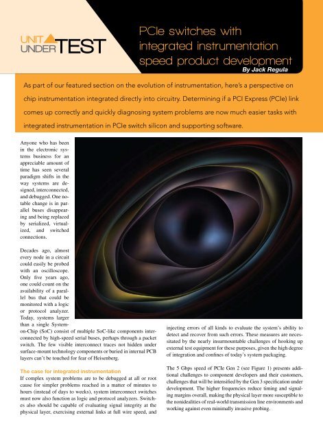
PCIe switches with integrated instrumentation speed product ...
PCIe switches with integrated instrumentation speed product ...
PCIe switches with integrated instrumentation speed product ...

Create successful ePaper yourself
Turn your PDF publications into a flip-book with our unique Google optimized e-Paper software.
UNIT<br />
UNDERTEST<br />
INNOVATION IN ELECTRONICS TEST TECHNOLOGY<br />
Anyone who has been<br />
in the electronic systems<br />
business for an<br />
appreciable amount of<br />
time has seen several<br />
paradigm shifts in the<br />
way systems are designed,<br />
interconnected,<br />
and debugged. One notable<br />
change is in parallel<br />
buses disappearing<br />
and being replaced<br />
by serialized, virtualized,<br />
and switched<br />
connections.<br />
Decades ago, almost<br />
every node in a circuit<br />
could easily be probed<br />
<strong>with</strong> an oscilloscope.<br />
Only five years ago,<br />
one could count on the<br />
availability of a parallel<br />
bus that could be<br />
monitored <strong>with</strong> a logic<br />
or protocol analyzer.<br />
Today, systems larger<br />
than a single Systemon-Chip<br />
(SoC) consist of multiple SoC-like components interconnected<br />
by high-<strong>speed</strong> serial buses, perhaps through a packet<br />
switch. The few visible interconnect traces not hidden under<br />
surface-mount technology components or buried in internal PCB<br />
layers can’t be touched for fear of Heisenberg.<br />
The case for <strong>integrated</strong> <strong>instrumentation</strong><br />
If complex system problems are to be debugged at all or root<br />
cause for simpler problems reached in a matter of minutes to<br />
hours (instead of days to weeks), system interconnect <strong>switches</strong><br />
must now also function as logic and protocol analyzers. Switches<br />
also should be capable of evaluating signal integrity at the<br />
physical layer, exercising external links at full wire <strong>speed</strong>, and<br />
<strong>PCIe</strong> <strong>switches</strong> <strong>with</strong><br />
<strong>integrated</strong> <strong>instrumentation</strong><br />
<strong>speed</strong> <strong>product</strong> development<br />
By Jack Regula<br />
As part of our featured section on the evolution of <strong>instrumentation</strong>, here’s a perspective on<br />
chip <strong>instrumentation</strong> <strong>integrated</strong> directly into circuitry. Determining if a PCI Express (<strong>PCIe</strong>) link<br />
comes up correctly and quickly diagnosing system problems are now much easier tasks <strong>with</strong><br />
<strong>integrated</strong> <strong>instrumentation</strong> in <strong>PCIe</strong> switch silicon and supporting software.<br />
injecting errors of all kinds to evaluate the system’s ability to<br />
detect and recover from such errors. These measures are necessitated<br />
by the nearly insurmountable challenges of hooking up<br />
external test equipment for these purposes, given the high degree<br />
of integration and confines of today’s system packaging.<br />
The 5 Gbps <strong>speed</strong> of <strong>PCIe</strong> Gen 2 (see Figure 1) presents additional<br />
challenges to component developers and their customers,<br />
challenges that will be intensified by the Gen 3 specification under<br />
development. The higher frequencies reduce timing and signaling<br />
margins overall, making the physical layer more susceptible to<br />
the nonidealities of real-world transmission line environments and<br />
working against even minimally invasive probing.
To overcome physical layer impairments, SERDES designers utilize<br />
the concept of receive equalization. Using equalization, the<br />
signal integrity eye opening is meaningfully observable only at the<br />
output of the equalizer, buried inside the component. This can only<br />
be done <strong>with</strong> the aid of <strong>integrated</strong> <strong>instrumentation</strong>.<br />
Accelerating <strong>product</strong> bring-up<br />
Experienced and successful design teams have long implemented<br />
features that allow them to debug problems that arise during the<br />
course of <strong>product</strong> development. With transistor densities available<br />
today, designers can integrate logic analysis capabilities alongside<br />
critical mission functions, often <strong>with</strong>out affecting cost. The ability<br />
to look at even a tiny subset of the logic nodes in a multimillion gate<br />
ASIC can be of inestimable value in quickly reaching the root cause<br />
of a component- or system-level bug.<br />
While once reserved for factory use only, these advanced capabilities<br />
are now being opened up to customers through software that<br />
provides a high-level interface. This interface frees the customer<br />
from the need to have detailed knowledge about circuit implementation<br />
in order to make sense of the results, while protecting the<br />
manufacturer’s intellectual property. At the same time, the scope<br />
of <strong>integrated</strong> analysis tools is expanding from a single component<br />
focus to system-wide issues.<br />
While <strong>integrated</strong> <strong>instrumentation</strong> is useful throughout the development<br />
cycle, its value can be appreciated most readily when considering<br />
the issues involved in initial board bring-up. When a system<br />
or subsystem consists of several SoCs surrounding a central <strong>PCIe</strong><br />
packet switch, the switch is the focus of attention after that first<br />
power-on. Have the links come up? Is signal integrity as predicted<br />
and required? Did enumeration and subsequent configuration<br />
succeed? Are the packet flow patterns nominal? The sooner these<br />
questions are answered, the sooner the team can zero in on what<br />
Murphy has thrown at them and move toward a successful <strong>product</strong><br />
release. With <strong>integrated</strong> <strong>instrumentation</strong> backed up by vendor-provided<br />
support software, these answers are readily available.<br />
Figure 1<br />
Using the internal logic analyzer<br />
The first order of business when powering on a new board is to<br />
determine if the <strong>PCIe</strong> links have come up. <strong>PCIe</strong> <strong>switches</strong> commonly<br />
provide a link status output for each port that can control an<br />
LED for visual indication. If a link doesn’t come up, it is extremely<br />
helpful to trace the transitions of the Link Training and Status State<br />
Machine (LTSSM) defined in the <strong>PCIe</strong> specification.<br />
A switch <strong>with</strong> even a simple <strong>integrated</strong> logic analyzer can be configured<br />
to capture and time-stamp each transition of a port’s LTSSM<br />
into internal trace memory during a link training cycle. Afterwards,<br />
the trace can be read out via I2C or <strong>PCIe</strong> and analyzed <strong>with</strong> the aid<br />
of supplied software. Such a trace can often quickly discriminate<br />
between an interoperability issue, manufacturing problem, and signal<br />
integrity issue.<br />
If tracing the LTSSM doesn’t identify the answer, an internal logic<br />
analyzer can be pointed first at the output of the SERDES’ serialto-parallel<br />
converter, elastic buffer, descrambler, and so forth in an<br />
attempt to pinpoint the malfunction.<br />
While an <strong>integrated</strong> logic analyzer may provide the ability to probe<br />
deep into the guts of an ASIC, only those registers or state machines<br />
either close to an external interface or architected as called<br />
for in an industry standard will be meaningful to an end user.<br />
Optimizing link performance<br />
Once each link is up, it’s necessary to estimate the signal integrity<br />
eye opening and optimize it. Advanced SERDES allow the width of<br />
the eye opening to be measured <strong>with</strong> the help of Built-In Self-Test<br />
(BIST) features. This is done using sometimes patented techniques<br />
that offset the sampling point from the center of the eye and then determine<br />
if this results in bit errors. Links are put in loopback mode<br />
and bit error rates tested using internal bit error rate test logic. The<br />
debug processor can step through settings of the SERDES equalizers<br />
and drive strength options, reporting the ones that work best<br />
and even burning them into an optional serial Electrically Erased<br />
Programmable Read-Only Memory (EEPROM) for automatic loading<br />
at the next power-on cycle.<br />
Software that provides a degree of automation<br />
to this measurement and parameter optimization<br />
process can be provided (see Figure 2).<br />
With a debug processor connected to the<br />
switch’s I2C bus, an engineer has sideband access<br />
to all the switch’s internal registers. The<br />
developer can peek and poke manually while<br />
the application is running to check its progress<br />
or cause a script to be executed that compares<br />
the actual switch configuration state to the expected<br />
one.<br />
The debug processor can configure available<br />
performance monitors and then display the<br />
collected statistics in real time while an application<br />
is running to give a real-time indication
UNIT<br />
UNDERTEST<br />
INNOVATION IN ELECTRONICS TEST TECHNOLOGY<br />
of its health. Purely as a matter of<br />
convenience, similar access can be<br />
provided through the debug port<br />
to downstream devices’ control<br />
and status registers. When used<br />
in this manner, the debug processor<br />
acts like the management or<br />
service processor used in servers<br />
and, indeed, their functions may<br />
be combined.<br />
Evolution of <strong>instrumentation</strong><br />
After functional debugging, stress<br />
testing and error injection are two<br />
necessary parts of <strong>product</strong> development.<br />
A switch’s normal data<br />
path is easily modified to function<br />
as an exerciser. As a first step, the<br />
switch sets aside a portion of its<br />
buffer memory, allows software<br />
to build packets therein, and then<br />
transmits the packets on a selected<br />
link. More advanced implementations<br />
include counting, looping,<br />
and branching mechanisms to support<br />
more complex packet streams<br />
and add a pseudorandom element to the error injection.<br />
When operating some portion of a switch as an exerciser, the<br />
ports involved no longer act as <strong>switches</strong>. Therefore, this capability<br />
is not as unobtrusive as other development acceleration<br />
features found in <strong>PCIe</strong> <strong>switches</strong>. Nevertheless, the simple availability<br />
of a component that can perform error injection and generate<br />
a full wire-<strong>speed</strong> packet stream on up to an x16 Gen 2 link<br />
is a huge boon to the <strong>product</strong> validation community.<br />
Implementing embedded <strong>instrumentation</strong><br />
At PLX Technology, integrating these capabilities into <strong>PCIe</strong> silicon<br />
evolved out of a selfish desire to reduce manufacturing costs<br />
and facilitate internal debug and validation efforts. It quickly<br />
became evident that these capabilities were perhaps even more<br />
valuable to customers for the accelerative<br />
effect on their <strong>product</strong> development process.<br />
Because technology is advancing<br />
to ever-higher interconnect <strong>speed</strong>s, PLX<br />
believes that <strong>integrated</strong> <strong>instrumentation</strong><br />
is fast becoming essential, especially for<br />
<strong>PCIe</strong> <strong>switches</strong>.<br />
Implementing the SERDES eye measurement<br />
capability requires close cooperation<br />
<strong>with</strong> both SERDES and SERDES BIST<br />
intellectual property vendors, then diligent<br />
work by design teams to exploit the<br />
capabilities thus provided.<br />
Implementing on-chip logic analysis is enabled<br />
by a design methodology that requires<br />
Figure 2<br />
Register Transfer Level (RTL) engineers to provide selectable probe<br />
output of critical states from each major module in much the<br />
same way that they are required to insert verification assertions.<br />
This internal standardization allows script development to partially<br />
automate the addition of the probe buses that feed into the<br />
trigger logic and trace memory into the RTL hierarchy. Standardization<br />
also reduces the software effort required to harness<br />
this data and shape at least some of it into a form that is useful<br />
to an end user.<br />
Integrated <strong>instrumentation</strong> and supporting software tools are<br />
showing excellent potential and becoming more user-friendly as<br />
the technology develops. This represents a new and promising<br />
direction for <strong>PCIe</strong> switch vendors and customers – one that can<br />
remove major sources of pain and delay from the system development<br />
process.<br />
Jack Regula is chief scientist at PLX Technology,<br />
based in Sunnyvale, California. An inventor of early<br />
switch fabric technology, he has delivered several<br />
technical presentations at industry conferences and<br />
authored multiple technical articles in leading trade<br />
publications. Jack received a BSEE (cum laude) and<br />
an MEE from Rensselaer Polytechnic University, an<br />
education funded by National Merit and New York<br />
State Regents scholarships, as well as the National<br />
Science Foundation.<br />
PLX Technology<br />
408-774-9060<br />
jregula@plxtech.com<br />
www.plxtech.com