conducters by Impact of EMP and UWB Pulses
conducters by Impact of EMP and UWB Pulses
conducters by Impact of EMP and UWB Pulses

Create successful ePaper yourself
Turn your PDF publications into a flip-book with our unique Google optimized e-Paper software.
Influence <strong>of</strong> the Technology on the Destruction Effects <strong>of</strong> Semi<strong>conducters</strong><br />
<strong>by</strong> <strong>Impact</strong> <strong>of</strong> <strong>EMP</strong> <strong>and</strong> <strong>UWB</strong> <strong>Pulses</strong><br />
Michael Camp<br />
University <strong>of</strong> Hanover<br />
Institute <strong>of</strong> Electrical Engineering<br />
<strong>and</strong> Measurement Science<br />
D-30167 Hanover, Germany<br />
email camp@ieee.org<br />
Abstract<br />
In this paper the influence <strong>of</strong> TTL- <strong>and</strong> CMOS-technology<br />
on the destruction effects <strong>of</strong> semi<strong>conducters</strong> <strong>by</strong> impact <strong>of</strong><br />
<strong>EMP</strong> <strong>and</strong> <strong>UWB</strong> pulses is determined. Different logic devices<br />
like NANDs <strong>and</strong> inverter were exposed to high amplitude<br />
transient pulses.<br />
Keywords<br />
<strong>UWB</strong>, <strong>EMP</strong>, Susceptibility, TTL, CMOS, Semiconductor<br />
I. INTRODUCTION<br />
The goal <strong>of</strong> this investigation is to measure the susceptibility<br />
<strong>of</strong> electronic devices to a transient electromagnetic<br />
field threat. Modern electronics are <strong>of</strong> vital importance for<br />
the function <strong>of</strong> traffic systems, security systems <strong>and</strong> modern<br />
communication. A malfunction in one <strong>of</strong> these areas<br />
could cause casualties <strong>and</strong> economic disasters. Nowadays<br />
HPM <strong>and</strong> <strong>UWB</strong> equipment can be bought <strong>by</strong> everyone.<br />
Taken the aspect <strong>of</strong> electromagnetic terrorism into account<br />
an <strong>UWB</strong> system could be a very dangerous weapon, because<br />
it can be built in a very small volume due to the low<br />
energy content <strong>of</strong> the pulse. Therefore the susceptibility <strong>of</strong><br />
electronics to pulsed electromagnetic fields like <strong>EMP</strong> <strong>and</strong><br />
<strong>UWB</strong> pulses is <strong>of</strong> great interest. The intention <strong>of</strong> this work<br />
is to analyze the influence <strong>of</strong> the semiconducter technology<br />
on the breakdown <strong>and</strong> destruction effects. On that account<br />
ten different technologies (six TTL- <strong>and</strong> four CMOS-<br />
Technologies) have been tested. Upon destructions have<br />
occured the devices were opened <strong>and</strong> scanned with an<br />
electron microscope to analyze the effects which takes<br />
place on the different technologies.<br />
II. GENERAL MEASUREMENT SETUP<br />
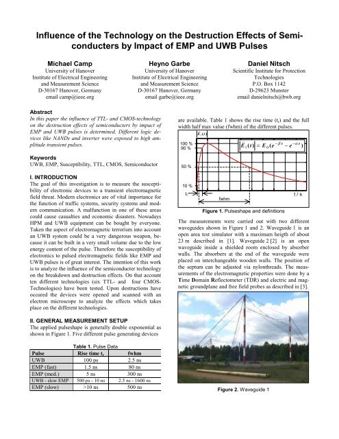
The applied pulseshape is generally double exponential as<br />
shown in Figure 1. Five different pulse generating devices<br />
Table 1. Pulse Data<br />
Pulse Rise time tr fwhm<br />
<strong>UWB</strong> 100 ps 2.5 ns<br />
<strong>EMP</strong> (fast) 1.5 ns 80 ns<br />
<strong>EMP</strong> (med.) 5 ns 300 ns<br />
<strong>UWB</strong> - slow <strong>EMP</strong> 500 ps - 10 ns 2.5 ns - 1600 ns<br />
<strong>EMP</strong> (slow) >10 ns 500 ns<br />
Heyno Garbe<br />
University <strong>of</strong> Hanover<br />
Institute <strong>of</strong> Electrical Engineering<br />
<strong>and</strong> Measurement Science<br />
D-30167 Hanover, Germany<br />
email garbe@ieee.org<br />
Daniel Nitsch<br />
Scientific Institute for Protection<br />
Technologies<br />
P.O. Box 1142<br />
D-29623 Munster<br />
email danielnitsch@bwb.org<br />
are available. Table 1 shows the rise time (tr) <strong>and</strong> the full<br />
width half max value (fwhm) <strong>of</strong> the different pulses.<br />
100 %<br />
90 %<br />
50 %<br />
10 %<br />
tr<br />
H<br />
E1(t )<br />
fwhm<br />
H<br />
E1<br />
( t ) = E 0 ( e<br />
Figure 1. <strong>Pulses</strong>hape <strong>and</strong> definitions<br />
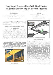
The measurements were carried out with two different<br />
waveguides shown in Figure 1 <strong>and</strong> 2. Waveguide 1 is an<br />
open area test simulator with a maximum heigth <strong>of</strong> about<br />
23 m described in [1]. Waveguide 2 [2] is an open<br />
waveguide inside a shielded room enclosed <strong>by</strong> absorber<br />
walls. The absorbers at the end <strong>of</strong> the waveguide were<br />
placed on interchangeable wooden walls. The position <strong>of</strong><br />
the septum can be adjusted via nylonthreads. The measurements<br />
<strong>of</strong> the electromagnetic properties were done <strong>by</strong> a<br />
Time Domain Reflectometer (TDR) <strong>and</strong> electric <strong>and</strong> magnetic<br />
groundplane <strong>and</strong> free field probes as described in [3].<br />
Figure 2. Waveguide 1<br />
− β t −α<br />
t<br />
− e<br />
t / s<br />
)
III. DEFINITIONS<br />
Figure 3. Waveguide 2<br />
III.1 Failure Rates<br />
To describe the different failure effects two quantities have<br />
been defined [5]. The Breakdown Failure Rate (BFR) has<br />
been defined as the number <strong>of</strong> breakdowns <strong>of</strong> a system,<br />
divided <strong>by</strong> the number <strong>of</strong> pulses applied to it. A<br />
breakdown means no physical damage is done to the<br />
system. After a reset (self-, external- or power reset) the<br />
system is going back into function.<br />
Table 2. Failure Rates<br />
Breakdown Destruction<br />
Delay Time<br />
Pulse Self-, External-,<br />
Power-Reset<br />
Breakdown Failure<br />
Rate<br />
No.<br />
<strong>of</strong> Breakdowns<br />
BFR =<br />
No.<br />
<strong>of</strong> <strong>Pulses</strong><br />
Pulse<br />
Destruction Failure<br />
Rate<br />
No.<br />
<strong>of</strong> Destructions<br />
DFR =<br />
No.<br />
<strong>of</strong> <strong>Pulses</strong><br />
The Destruction Failure Rate (DFR) <strong>of</strong> the device under<br />
test has been defined as the number <strong>of</strong> destructions divided<br />
<strong>by</strong> the number <strong>of</strong> pulses applied to the system. Destruction<br />
is defined as a physical damage <strong>of</strong> the system so that the<br />
system will not recover without a hardware repair.<br />
III.2 Principle Behavior <strong>of</strong> BFR <strong>and</strong> DFR<br />
The BFR <strong>and</strong> DFR behaves in principle as shown in<br />
Figure 4. As important parameters for the description <strong>of</strong><br />
the susceptibility <strong>of</strong> a system four quantities were defined.<br />
The Breakdown Threshold (BT) specifies the value <strong>of</strong> the<br />
electrical field strength, at which the BFR gets 5% <strong>of</strong> the<br />
maximum value. The Breakdown B<strong>and</strong>width (BB) is<br />
defined as the span <strong>of</strong> the electrical field strength, in which<br />
the BFR changes from 5% to 95% <strong>of</strong> the maximum.<br />
Äquivalent definitions were done for the destruction<br />
failure rate DFR (compare Figure 4).<br />
BFR<br />
DFR<br />
1<br />
0,95<br />
0,05<br />
0<br />
Figure 4. BFR, DFR - principle behavior <strong>and</strong> definitions<br />
IV. SUSCEPTIBILITY OF LOGIC-DEVICES<br />
During the investigations ten different semiconductor<br />
technologies (six TTL-, four CMOS-families) have been<br />
tested (Table 3) concerning the susceptibility to <strong>EMP</strong> <strong>and</strong><br />
<strong>UWB</strong> pulses. NANDs, inverter, generic array logic devices<br />
<strong>and</strong> shift registers were choosen to observe the influence <strong>of</strong><br />
the technology on the destruction effects.<br />
St<strong>and</strong>ard Schottky<br />
(S)<br />
High Speed<br />
(HC)<br />
BFR<br />
Breakdown<br />
B<strong>and</strong>width<br />
BB<br />
Breakdown<br />
Threshold<br />
BT<br />
Table 3. Tested Technologies<br />
TTL-Technology<br />
Low<br />
Power<br />
Schottky<br />
(LS)<br />
Advanced<br />
Schottky<br />
(AS)<br />
CMOS-Technology<br />
High Speed<br />
TTL-compatibel<br />
(HCT)<br />
DFR<br />
Advanced<br />
(AC)<br />
Destruction<br />
B<strong>and</strong>width<br />
DT<br />
Destruction<br />
Threshold<br />
DT<br />
Advanced<br />
Low<br />
Power<br />
Schottky<br />
(ALS)<br />
Amplitude<br />
Fairchild<br />
Advanced<br />
Schottky<br />
(FAST)<br />
Advanced<br />
TTL-compatibel<br />
(ACT)<br />
IV.1 Test Setup<br />
To apply the different pulses to the EUT a modular setup<br />
has been realized (Figure 5). Ten separate channels were<br />
built with a combination <strong>of</strong> differently printed circuit<br />
boards. The circuit boards were combined with ribbon<br />
cables to realize different coupling lengths at the input <strong>and</strong><br />
output pins <strong>of</strong> the devices under test.
St<strong>and</strong>ard<br />
TTL<br />
Accu 1 Accu2<br />
Power supply<br />
Accu 10<br />
Logic 1<br />
Buffer<br />
Load 1<br />
FAST<br />
TTL<br />
...<br />
. . .<br />
Logic 2 Logic circuits<br />
Logic 10<br />
. . .<br />
E L<br />
H L<br />
S L<br />
Buffer Buffer circuits<br />
Buffer<br />
. . .<br />
10 separate Channels<br />
ribbon cables<br />
Load 2<br />
Loads<br />
(LEDs + Resistors) Load 10<br />
Figure 5. Test Setup - Principle<br />
In Fig.6 a NAND test setup with 20 cm ribbon cable length<br />
at the input pins <strong>and</strong> ≈ 0 cm ribbon cable length at the output<br />
pins <strong>of</strong> the test devices is shown. The power supply is<br />
realized with ten different accumulators. DIP switches<br />
were implemented to the power supply unit to adjust arbitrary<br />
bit patterns at the input pins. LEDs <strong>and</strong> resistors were<br />
used as loads to observe the operating states <strong>of</strong> the devices.<br />
H power supply<br />
L<br />
S L<br />
E L<br />
ribbon cables<br />
loads<br />
DIP switches<br />
logic devices<br />
Figure 6. NAND Test Setup - Realization<br />
HCT<br />
CMOS<br />
IV.2 Measurement Results<br />
As a first result it can be noticed, that CMOS-devices first<br />
gets reversible breakdowns which can be reversed <strong>by</strong><br />
switching the power <strong>of</strong>f <strong>and</strong> on again. At much higher field<br />
amplitudes non reversible destructions occur. This effect<br />
can be explained <strong>by</strong> a parasitic thyristor as a result <strong>of</strong> the<br />
vicinity <strong>of</strong> complementary n- <strong>and</strong> p-channel transistors in<br />
CMOS devices described in [5]. Figure 7 shows the BFR<br />
<strong>and</strong> DFR <strong>of</strong> NAND-devices built in four different CMOS<br />
technologies.<br />
1<br />
0,8<br />
0,6<br />
0,4<br />
0,2<br />
0<br />
BFR<br />
DFR<br />
CMOS<br />
0 200 400 600 800 1000 1200 1400<br />
E in kV/m<br />
HCT HC ACT AC<br />
HCT HC ACT AC<br />
Figure 7. Breakdown (BFR) <strong>and</strong> Destruction Failure Rate<br />
(DFR) <strong>of</strong> CMOS NAND Devices<br />
The comparison <strong>of</strong> CMOS- with TTL-NAND-devices<br />
shows, that the destruction thresholds are similar, but that<br />
TTL-NAND-devices only get non reversible destructions<br />
<strong>and</strong> at lower field amplitudes no breakdowns occured<br />
(Figure 8) in contrary to the behavior <strong>of</strong> CMOS-NANDdevices.<br />
1<br />
0,8<br />
0,6<br />
0,4<br />
0,2<br />
0<br />
0 200 400 600 800 1000 1200 1400<br />
E in kV/m<br />
St<strong>and</strong>ard S ALS<br />
AS LS F<br />
DFR<br />
TTL<br />
Figure 8. Destruction Failure Rate (DFR) <strong>of</strong> TTL NAND<br />
Devices
Figure 9 shows the Breakdown- (BT) <strong>and</strong> Destruction<br />
threshold (DT) <strong>of</strong> NAND-devices built in ten different<br />
technologies (compare Table 3). The same effects were<br />
observed during the investigation <strong>of</strong> inverter devices.<br />
800<br />
600<br />
400<br />
200<br />
0<br />
St<strong>and</strong>ard TTL<br />
Figure 9. Breakdown (BT) <strong>and</strong> Destruction (DT) Threshold<br />
<strong>of</strong> CMOS <strong>and</strong> TTL NAND Devices<br />
V. MICROSCOPIC ANALYSIS<br />
V.1 Destruction Effects<br />
The microscopic analysis <strong>of</strong> the destructed devices generally<br />
shows three different damaging effects (Fig. 10). At<br />
lower field strengths only electronic components like diodes<br />
or transistors on the chip, mostly as a result <strong>of</strong> flashover<br />
effects, were damaged (Fig. 10a). If the amplitude <strong>of</strong><br />
the electromagnetic pulse increases <strong>by</strong> about 50 %, additional<br />
onchipwire destructions (this means smelting <strong>of</strong> pcb<br />
tracks without flashover effects) <strong>and</strong> multiple component<br />
destructions occured (Fig. 10b). Further increase <strong>of</strong> the<br />
amplitude leads to additional bondwire destructions<br />
(Fig. 10c) <strong>and</strong> multiple component- <strong>and</strong> onchipwiredestructions.<br />
a)<br />
c)<br />
Schottky TTL<br />
BT in kV/m DT in kV/m<br />
LS-TTL<br />
AS-TTL<br />
Diode<br />
ALS-TTL<br />
Component Destruction<br />
Bondwire Destruction<br />
Fast-TTL<br />
HC (CMOS)<br />
b)<br />
HCT (CMOS)<br />
AC (CMOS)<br />
Figure 10. Destruction effects on chip level<br />
ACT (CMOS)<br />
Onchipwire Destr.<br />
Figure 11 shows an TTL NAND device with multiple<br />
component- onchip- <strong>and</strong> bondwire destructions after impact<br />
<strong>of</strong> an <strong>EMP</strong> with tr = 7.5 ns, tfwhm = 180 ns <strong>and</strong> an amplitude<br />
<strong>of</strong> about 1300 kV/m electrical field strength. The<br />
ribbon cable length at the input pins was ≈ 20 cm. At the<br />
output pins ≈ 0 cm ribbon cable length was realized (compare<br />
Fig. 6).<br />
Figure 11. NAND Device with multiple Destructions<br />
Simular results were observed during the investigations <strong>of</strong><br />
TTL-Inverter devices. Figure 12 shows the destruction<br />
failure rate (DFR) <strong>of</strong> TTL-Inverter devices, separated to<br />
component-, onchipwire- <strong>and</strong> bondwire-destructions. At<br />
the lowest field level component destructions occured. A<br />
further rising <strong>of</strong> the field strength resulted in onchipwire<strong>and</strong><br />
bondwire-destructions.<br />
1<br />
0,8<br />
0,6<br />
0,4<br />
0,2<br />
0<br />
DFR<br />
Components<br />
Std.<br />
S<br />
ALS<br />
LS<br />
Onchipwires<br />
Bondwires<br />
Components<br />
Onchipwires<br />
Bondwires<br />
Std.<br />
S<br />
ALS<br />
LS<br />
Std.<br />
S<br />
ALS<br />
LS<br />
0 200 400 600 800 1000 1200 1400<br />
E in kV/m<br />
Figure 12. DFR <strong>of</strong> TTL-NAND-Devices separated into<br />
Component- Bondwire- <strong>and</strong> Onchipwire-Destructions<br />
V.2 Component Destructions<br />
Depending on the technology <strong>and</strong> the manufacturer, different<br />
component destruction effects have occured. Figure 13<br />
for example shows an 74S00 TTL NAND device with four<br />
component destructions after the impact <strong>of</strong> an <strong>EMP</strong>
(tr = 7.5 ns, fwhm = 180 ns, amplitude = 650 kV/m). All<br />
bondwires <strong>and</strong> onchipwires are intact.<br />
Figure 13. Schottky-TTL NAND with Component-<br />
Destructions<br />
Type 74xx00 devices are composed <strong>of</strong> four separate<br />
NAND gates with combined VCC <strong>and</strong> Ground pins.<br />
NAND 1 <strong>and</strong> 2 as well as NAND 3 <strong>and</strong> 4 are manufactured<br />
with symmetry to the x-y axis. At NAND 1 <strong>and</strong> 2 as<br />
well as NAND 3 <strong>and</strong> 4 the same components have been<br />
destructed. In Figure 14 <strong>and</strong> Figure 15 for example the<br />
damaged areas <strong>of</strong> NAND 1 <strong>and</strong> 2 is shown. Between point<br />
P1 <strong>and</strong> point P2, marked in Fig. 14-16, a flashover has<br />
occured <strong>and</strong> as a result the metallic structure at the top<br />
layer directly around two distributed resistors (R1 <strong>and</strong> R2<br />
in the depth <strong>of</strong> the material, not visible) has been destroyed<br />
<strong>and</strong> affected the two resistors.<br />
A2<br />
Schottky-TTL NAND<br />
NAND1<br />
P1<br />
not damaged<br />
A1 A3<br />
P2<br />
Destructions<br />
damaged<br />
NAND3<br />
X<br />
A2<br />
A4<br />
Y<br />
NAND2 NAND4<br />
Figure 14. Schottky -TTL NAND - Destruction in Detail<br />
The fact, that always this area was damaged first, leads to<br />
the conclusion, that the dameged zone shown in Fig. 14<br />
<strong>and</strong> 15 is the most susceptible area <strong>of</strong> the Schottky-TTL-<br />
NAND in this configuration <strong>and</strong> layout.<br />
A2<br />
not damaged<br />
Figure 15. Schottky-TTL NAND - Destruction in Detail<br />
Figure 16 shows the basic schematic <strong>of</strong> a Schottky TTL<br />
NAND device <strong>and</strong> the area where the flashover has occured.<br />
At lower field strengths the resistors R1 <strong>and</strong> R2<br />
have always been destructed first.<br />
P2<br />
P1<br />
P2<br />
R1 R2<br />
Figure 16. Schottky TTL NAND - Schematic<br />
Similar effects were observed with the other technologies.<br />
The components on the chip, which were damaged first if<br />
the amplitude <strong>of</strong> the electromagnetic pulse was increased,<br />
are depending on the layout <strong>of</strong> the chip (<strong>and</strong> therefore on<br />
the manufactorer) as well as on the technology. Transistors,<br />
diodes <strong>and</strong> resistors were damaged similarly.<br />
V.2 Onchipwire Destructions<br />
damaged<br />
+VCC<br />
Input<br />
T4<br />
A<br />
B<br />
T1 T2 R4 Output<br />
Y<br />
R5<br />
P1<br />
A further rising <strong>of</strong> the amplitude <strong>of</strong> the electromagnetic<br />
pulse resulted in onchipwire destructions. Figure 17 shows<br />
different onchipwire destructions after the impact <strong>of</strong> an<br />
<strong>EMP</strong> with tr = 7.5 ns, tfwhm = 180 ns <strong>and</strong> an amplitude <strong>of</strong><br />
about 900 kV/m electrical field strength.<br />
T3<br />
T6<br />
R6<br />
T5<br />
R3
a)<br />
Figure 17. Destruction <strong>of</strong> Onchipwires<br />
V.3 Bondwire Destructions<br />
Bondwire destructions always occured at higher pulse amplitudes<br />
than onchipwire destructions due to the fact, that<br />
onchipwires normaly has much lower cross sections than<br />
bondwires. The destructions occured <strong>by</strong> melting <strong>of</strong> the<br />
material similar to onchipwire destructions. Figure 18<br />
shows two destructed bondwires <strong>and</strong> pads.<br />
a) b)<br />
Figure 18. Destructions <strong>of</strong> Bondwires<br />
The energy to destruct bond- or onchipwires can be calculated<br />
via the equation [5]<br />
( melt sur ) T T c l A Q − ⋅ ⋅ ⋅ ⋅ = ρ<br />
with A = cross section, l = length <strong>of</strong> wire, ρ = density <strong>of</strong><br />
material, c = specific heat capacity, Tmelt = melting temperature<br />
<strong>and</strong> Tsur = surrounding area temperature. Equation<br />
1 shows that the melting energy strictly depends on the<br />
cross section, if the same material is used for bond- <strong>and</strong><br />
onchipwires under the constraint heat transfer into the surrounding<br />
area is neglectable (valid due to short pulse impact).<br />
Drawing an energy balance results in equation 2<br />
which allows to make a rough estimate <strong>of</strong> the current<br />
which was responsible for the bondwire destruction.<br />
b)<br />
(1)<br />
I =<br />
With κ = electrical conductivity, d = diameter <strong>of</strong> the<br />
bondwires <strong>and</strong> the assumption that the duration <strong>of</strong> the current<br />
is approximately equivalent to the pulse length, a current<br />
<strong>of</strong> I ≈ 400 A can be calculated via equation 2 if<br />
bondwires made <strong>of</strong> aluminium were implemented.<br />
VI. SUMMARY<br />
The investigation <strong>of</strong> the susceptibility <strong>of</strong> logic devices built<br />
in ten different semiconductor technologies (NANDs <strong>and</strong><br />
Inverter) to <strong>EMP</strong> <strong>and</strong> <strong>UWB</strong> pulses has shown, that CMOS<br />
devices first gets reversible breakdowns <strong>and</strong> at much<br />
higher field amplitudes non reversible destructions occur.<br />
The destruction thresholds <strong>of</strong> TTL <strong>and</strong> CMOS devices are<br />
similar but TTL devices always gets non reversible destructions.<br />
The breakdown- (BT) <strong>and</strong> destructionthresholds<br />
(DT) decreases much <strong>by</strong> extending the ribbon<br />
cable length or usage <strong>of</strong> pulses with faster rise times.<br />
The destruction effects can be separated into componentonchipwire-<br />
<strong>and</strong> bondwire-destructions. First, at lower<br />
field amplitudes, component destructions ,mostly as a result<br />
<strong>of</strong> flashover effects, occur. If the amplitude increases<br />
also onchipwire destructions appear. Further increase <strong>of</strong><br />
the amplitude is leading to additional bondwire destructions<br />
<strong>and</strong> multiple component- <strong>and</strong> onchipwiredestructions.<br />
This investigation is part <strong>of</strong> the study “Susceptibility <strong>of</strong><br />
Electronics to <strong>EMP</strong> <strong>and</strong> <strong>UWB</strong>, Phase II”, commissioned<br />
<strong>by</strong> the Armed Forces Scientific Institute for Protection<br />
Technologies - ABC-Protection (Munster, Germany).<br />
REFERENCES<br />
2 4<br />
ρ ⋅κ<br />
⋅c<br />
⋅π<br />
⋅d<br />
⋅(<br />
T<br />
16⋅<br />
∆t<br />
melt<br />
−T<br />
[1] D.Nitsch, J.Schlüter, H.J.Kitschke, “Generierung<br />
und Vorteile von Ultrawideb<strong>and</strong>-Impulsen”,<br />
EMV99, Mannheim, Germany<br />
[2] C.Braun, “Aufbau eines breitb<strong>and</strong>igen Wellenleiters<br />
für N<strong>EMP</strong> Modell Simulationen”, INT Bericht<br />
Okt. 84<br />
[3] D.Nitsch, M.Camp, "<strong>UWB</strong> <strong>and</strong> <strong>EMP</strong> Susceptibility<br />
<strong>of</strong> Modern Microprocessorboards", EMC<br />
Europe, Brugge, Sept. 2000<br />
[4] M.Camp, H.Garbe, D.Nitsch, "<strong>UWB</strong> <strong>and</strong> <strong>EMP</strong><br />
Susceptibility <strong>of</strong> Modern Electronics", IEEE<br />
EMC, Montreal, August 13-17, 2001, ISBN: 0-<br />
7803-6569-0, pp. 1015-1020<br />
[5] M.Camp, “Empfindlichkeit von Elektronik gegen<br />
<strong>EMP</strong> und <strong>UWB</strong> - Phase II”, WIS Bericht,<br />
Okt. 01, AN:005.H-0 A064, AG:UT 243-C<br />
sur<br />
)<br />
(2)