
You also want an ePaper? Increase the reach of your titles
YUMPU automatically turns print PDFs into web optimized ePapers that Google loves.
Features summary<br />
uPSD34xx<br />
Turbo Plus Series<br />
Fast Turbo 8032 MCU with USB and Programmable Logic<br />
■ Fast 8-bit Turbo 8032 MCU, 40 MHz<br />
– Advanced core, 4-clocks per instruction<br />
– 10 MIPs peak performance at 40MHz (5V)<br />
– JTAG Debug and In-System Programming<br />
– 16-bit internal instruction path fetches<br />
double-byte instruction in a single memory<br />
cycle<br />
– Branch Cache & 4 instruction Prefetch<br />
Queue<br />
– Dual XDATA pointers with automatic<br />
increment and decrement<br />
– Compatible with 3rd party 8051 tools<br />
■ Dual Flash memories with memory<br />
management<br />
– Place either memory into 8032 program<br />
address space or data address space<br />
– READ-while-WRITE operation for In-<br />
Application Programming and EEPROM<br />
emulation<br />
– Single voltage program and erase<br />
– 100K guaranteed erase cycles, 15-year<br />
retention<br />
■ Clock, reset, and power supply management<br />
– SRAM is Battery Backup capable<br />
– Flexible 8-level CPU clock divider register<br />
– Normal, Idle, and Power Down Modes<br />
– Power-on and Low Voltage reset supervisor<br />
– Programmable Watchdog Timer<br />
■ Programmable logic, general purpose<br />
– 16 macrocells for logic applications (e.g.,<br />
shifters, state machines, chip-selects, gluelogic<br />
to keypads, and LCDs)<br />
■ A/D converter<br />
– Eight Channels, 10-bit resolution, 6µs<br />
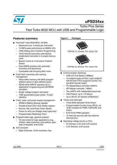
Figure 1. Packages<br />
TQFP52 (T), 52-lead, Thin, Quad, Flat<br />
TQFP80 (U), 80-lead, Thin, Quad, Flat<br />
■ Communication interfaces<br />
– USB v2.0 Full Speed (12Mbps)<br />
– 10 endpoint pairs (In/Out), each endpoint<br />
with 64-byte FIFO (supports Control, Intr,<br />
and Bulk transfer types)<br />
– I 2 C Master/Slave controller, 833kHz<br />
– SPI Master controller, 10MHz<br />
– Two UARTs with independent baud rate<br />
– IrDA Potocol: up to 115 kbaud<br />
– Up to 46 I/O, 5V tolerant uPSD34xxV<br />
■ Timers and interrupts<br />
– Three 8032 standard 16-bit timers<br />
– Programmable Counter Array (PCA), six<br />
16-bit modules for PWM, CAPCOM, and<br />
timers<br />
– 8/10/16-bit PWM operation<br />
– 12 Interrupt sources with two external<br />
interrupt pins<br />
■ Operating voltage source (±10%)<br />
– 5V Devices: 5.0V and 3.3V sources<br />
– 3.3V Devices: 3.3V source<br />
July 2006 Rev 4 1/293<br />
www.st.com<br />
293
Table 1. Device Summary<br />
Note: Operating temperature is in the Industrial range (–40°C to 85°C).<br />
2/293<br />
Part Number<br />
Max<br />
MHz<br />
1st<br />
Flash<br />
2nd<br />
Flash<br />
(bytes)<br />
SRAM<br />
GPIO<br />
8032<br />
Bus<br />
uPSD34xx<br />
V CC V DD Pkg.<br />
uPSD3422E-40T6 40 64K 32K 4K 35 No 3.3V 5.0V TQFP52<br />
uPSD3422EV-40T6 40 64K 32K 4K 35 No 3.3V 3.3V TQFP52<br />
uPSD3422E-40U6 40 64K 32K 4K 46 Yes 3.3V 5.0V TQFP80<br />
uPSD3422EV-40U6 40 64K 32K 4K 46 Yes 3.3V 3.3V TQFP80<br />
uPSD3433E-40T6 40 128K 32K 8K 35 No 3.3V 5.0V TQFP52<br />
uPSD3433EV-40T6 40 128K 32K 8K 35 No 3.3V 3.3V TQFP52<br />
uPSD3433E-40U6 40 128K 32K 8K 46 Yes 3.3V 5.0V TQFP80<br />
uPSD3433EV-40U6 40 128K 32K 8K 46 Yes 3.3V 3.3V TQFP80<br />
uPSD3434E-40T6 40 256K 32K 8K 35 No 3.3V 5.0V TQFP52<br />
uPSD3434EV-40T6 40 256K 32K 8K 35 No 3.3V 3.3V TQFP52<br />
uPSD3434E-40U6 40 256K 32K 8K 46 Yes 3.3V 5.0V TQFP80<br />
uPSD3434EV-40U6 40 256K 32K 8K 46 Yes 3.3V 3.3V TQFP80<br />
uPSD3454E-40T6 40 256K 32K 32K 35 No 3.3V 5.0V TQFP52<br />
uPSD3454EV-40T6 40 256K 32K 32K 35 No 3.3V 3.3V TQFP52<br />
uPSD3454E-40U6 40 256K 32K 32K 46 Yes 3.3V 5.0V TQFP80<br />
uPSD3454EV-40U6 40 256K 32K 32K 46 Yes 3.3V 3.3V TQFP80<br />
uPSD3422EB40T6 40 64K 32K 4K 35 No 3.3V 5.0V TQFP52<br />
uPSD3422EVB40T6 40 64K 32K 4K 35 No 3.3V 3.3V TQFP52<br />
uPSD3422EB40U6 40 64K 32K 4K 46 Yes 3.3V 5.0V TQFP80<br />
uPSD3422EVB40U6 40 64K 32K 4K 46 Yes 3.3V 3.3V TQFP80<br />
uPSD3433EB40T6 40 128K 32K 8K 35 No 3.3V 5.0V TQFP52<br />
uPSD3433EVB40T6 40 128K 32K 8K 35 No 3.3V 3.3V TQFP52<br />
uPSD3433EB40U6 40 128K 32K 8K 46 Yes 3.3V 5.0V TQFP80<br />
uPSD3433EVB40U6 40 128K 32K 8K 46 Yes 3.3V 3.3V TQFP80<br />
uPSD3434EB40T6 40 256K 32K 8K 35 No 3.3V 5.0V TQFP52<br />
uPSD3434EVB40T6 40 256K 32K 8K 35 No 3.3V 3.3V TQFP52<br />
<strong>uPSD3434EB40U6</strong> 40 256K 32K 8K 46 Yes 3.3V 5.0V TQFP80<br />
uPSD3434EVB40U6 40 256K 32K 8K 46 Yes 3.3V 3.3V TQFP80<br />
uPSD3454EB40T6 40 256K 32K 32K 35 No 3.3V 5.0V TQFP52<br />
uPSD3454EVB40T6 40 256K 32K 32K 35 No 3.3V 3.3V TQFP52<br />
uPSD3454EB40U6 40 256K 32K 32K 46 Yes 3.3V 5.0V TQFP80<br />
uPSD3454EVB40U6 40 256K 32K 32K 46 Yes 3.3V 3.3V TQFP80
uPSD34xx Contents<br />
Contents<br />
1 Summary description . . . . . . . . . . . . . . . . . . . . . . . . . . . . . . . . . . . . . . . . 9<br />
2 Pin descriptions . . . . . . . . . . . . . . . . . . . . . . . . . . . . . . . . . . . . . . . . . . . 11<br />
3 Hardware description . . . . . . . . . . . . . . . . . . . . . . . . . . . . . . . . . . . . . . . 17<br />
4 Memory organization . . . . . . . . . . . . . . . . . . . . . . . . . . . . . . . . . . . . . . . 19<br />
4.1 Internal memory (MCU module, standard 8032 memory: DATA, IDATA, SFR)<br />
20<br />
4.2 External memory (PSD module: program memory, data memory) . . . . . 20<br />
5 8032 MCU core performance enhancements . . . . . . . . . . . . . . . . . . . . 23<br />
5.1 Pre-fetch queue (PFQ) and branch cache (BC) . . . . . . . . . . . . . . . . . . . . 24<br />
5.2 PFQ example, multi-cycle instructions . . . . . . . . . . . . . . . . . . . . . . . . . . . 25<br />
5.3 Aggregate performance . . . . . . . . . . . . . . . . . . . . . . . . . . . . . . . . . . . . . . 25<br />
6 MCU module description . . . . . . . . . . . . . . . . . . . . . . . . . . . . . . . . . . . . 27<br />
7 8032 MCU registers . . . . . . . . . . . . . . . . . . . . . . . . . . . . . . . . . . . . . . . . . 28<br />
7.1 Stack pointer (SP) . . . . . . . . . . . . . . . . . . . . . . . . . . . . . . . . . . . . . . . . . . 28<br />
7.2 Data pointer (DPTR) . . . . . . . . . . . . . . . . . . . . . . . . . . . . . . . . . . . . . . . . . 28<br />
7.3 Program counter (PC) . . . . . . . . . . . . . . . . . . . . . . . . . . . . . . . . . . . . . . . 28<br />
7.4 Accumulator (ACC) . . . . . . . . . . . . . . . . . . . . . . . . . . . . . . . . . . . . . . . . . 28<br />
7.5 B register (B) . . . . . . . . . . . . . . . . . . . . . . . . . . . . . . . . . . . . . . . . . . . . . . 29<br />
7.6 General purpose registers (R0 - R7) . . . . . . . . . . . . . . . . . . . . . . . . . . . . 29<br />
7.7 Program status word (PSW) . . . . . . . . . . . . . . . . . . . . . . . . . . . . . . . . . . . 29<br />
8 Special function registers (SFR) . . . . . . . . . . . . . . . . . . . . . . . . . . . . . . 31<br />
9 8032 addressing modes . . . . . . . . . . . . . . . . . . . . . . . . . . . . . . . . . . . . . 38<br />
9.1 Register Addressing . . . . . . . . . . . . . . . . . . . . . . . . . . . . . . . . . . . . . . . . . 38<br />
9.2 Direct Addressing . . . . . . . . . . . . . . . . . . . . . . . . . . . . . . . . . . . . . . . . . . . 38<br />
9.3 Register Indirect Addressing . . . . . . . . . . . . . . . . . . . . . . . . . . . . . . . . . . 38<br />
9.4 Immediate Addressing . . . . . . . . . . . . . . . . . . . . . . . . . . . . . . . . . . . . . . . 39<br />
3/293
Contents uPSD34xx<br />
4/293<br />
9.5 External Direct Addressing . . . . . . . . . . . . . . . . . . . . . . . . . . . . . . . . . . . . 39<br />
9.6 External Indirect Addressing . . . . . . . . . . . . . . . . . . . . . . . . . . . . . . . . . . 39<br />
9.7 Indexed Addressing . . . . . . . . . . . . . . . . . . . . . . . . . . . . . . . . . . . . . . . . . 39<br />
9.8 Relative Addressing . . . . . . . . . . . . . . . . . . . . . . . . . . . . . . . . . . . . . . . . . 40<br />
9.9 Absolute Addressing . . . . . . . . . . . . . . . . . . . . . . . . . . . . . . . . . . . . . . . . 40<br />
9.10 Long Addressing . . . . . . . . . . . . . . . . . . . . . . . . . . . . . . . . . . . . . . . . . . . 40<br />
9.11 Bit Addressing . . . . . . . . . . . . . . . . . . . . . . . . . . . . . . . . . . . . . . . . . . . . . 40<br />
10 uPSD34xx instruction set summary . . . . . . . . . . . . . . . . . . . . . . . . . . . 42<br />
11 Dual data pointers . . . . . . . . . . . . . . . . . . . . . . . . . . . . . . . . . . . . . . . . . . 47<br />
11.1 Data pointer control register, DPTC (85h) . . . . . . . . . . . . . . . . . . . . . . . . 47<br />
11.2 Data pointer mode register, DPTM (86h) . . . . . . . . . . . . . . . . . . . . . . . . . 48<br />
12 Debug unit . . . . . . . . . . . . . . . . . . . . . . . . . . . . . . . . . . . . . . . . . . . . . . . . 50<br />
13 Interrupt system . . . . . . . . . . . . . . . . . . . . . . . . . . . . . . . . . . . . . . . . . . . 52<br />
13.1 Individual interrupt sources . . . . . . . . . . . . . . . . . . . . . . . . . . . . . . . . . . . 55<br />
14 MCU clock generation . . . . . . . . . . . . . . . . . . . . . . . . . . . . . . . . . . . . . . . 59<br />
14.1 MCU_CLK . . . . . . . . . . . . . . . . . . . . . . . . . . . . . . . . . . . . . . . . . . . . . . . . 59<br />
14.2 PERIPH_CLK . . . . . . . . . . . . . . . . . . . . . . . . . . . . . . . . . . . . . . . . . . . . . . 59<br />
15 Power saving modes . . . . . . . . . . . . . . . . . . . . . . . . . . . . . . . . . . . . . . . . 63<br />
15.1 Idle Mode . . . . . . . . . . . . . . . . . . . . . . . . . . . . . . . . . . . . . . . . . . . . . . . . . 63<br />
15.2 Power-down Mode . . . . . . . . . . . . . . . . . . . . . . . . . . . . . . . . . . . . . . . . . . 64<br />
15.3 Reduced Frequency Mode . . . . . . . . . . . . . . . . . . . . . . . . . . . . . . . . . . . . 64<br />
16 Oscillator and external components . . . . . . . . . . . . . . . . . . . . . . . . . . . 67<br />
17 I/O ports of mcu module . . . . . . . . . . . . . . . . . . . . . . . . . . . . . . . . . . . . . 69<br />
17.1 MCU port operating modes . . . . . . . . . . . . . . . . . . . . . . . . . . . . . . . . . . . 69<br />
18 MCU bus interface . . . . . . . . . . . . . . . . . . . . . . . . . . . . . . . . . . . . . . . . . . 78<br />
18.1 PSEN bus cycles . . . . . . . . . . . . . . . . . . . . . . . . . . . . . . . . . . . . . . . . . . . 78<br />
18.2 READ or WRITE bus cycles . . . . . . . . . . . . . . . . . . . . . . . . . . . . . . . . . . . 78
uPSD34xx Contents<br />
18.3 Connecting external devices to the MCU bus . . . . . . . . . . . . . . . . . . . . . 78<br />
18.4 Programmable bus timing . . . . . . . . . . . . . . . . . . . . . . . . . . . . . . . . . . . . . 79<br />
18.5 Controlling the PFQ and BC . . . . . . . . . . . . . . . . . . . . . . . . . . . . . . . . . . . 80<br />
19 Supervisory functions . . . . . . . . . . . . . . . . . . . . . . . . . . . . . . . . . . . . . . 83<br />
19.1 External reset input pin, RESET_IN . . . . . . . . . . . . . . . . . . . . . . . . . . . . . 83<br />
19.2 Low VCC voltage detect, LVD . . . . . . . . . . . . . . . . . . . . . . . . . . . . . . . . . . 84<br />
19.3 Power-up reset . . . . . . . . . . . . . . . . . . . . . . . . . . . . . . . . . . . . . . . . . . . . . 84<br />
19.4 JTAG debug reset . . . . . . . . . . . . . . . . . . . . . . . . . . . . . . . . . . . . . . . . . . . 84<br />
19.5 Watchdog timer, WDT . . . . . . . . . . . . . . . . . . . . . . . . . . . . . . . . . . . . . . . 84<br />
20 Standard 8032 timer/counters . . . . . . . . . . . . . . . . . . . . . . . . . . . . . . . . 87<br />
20.1 Standard timer SFRs . . . . . . . . . . . . . . . . . . . . . . . . . . . . . . . . . . . . . . . . 87<br />
20.2 Clock sources . . . . . . . . . . . . . . . . . . . . . . . . . . . . . . . . . . . . . . . . . . . . . . 87<br />
20.3 SFR, TCON . . . . . . . . . . . . . . . . . . . . . . . . . . . . . . . . . . . . . . . . . . . . . . . 88<br />
20.4 SFR, TMOD . . . . . . . . . . . . . . . . . . . . . . . . . . . . . . . . . . . . . . . . . . . . . . . 89<br />
20.5 Timer 0 and Timer 1 operating modes . . . . . . . . . . . . . . . . . . . . . . . . . . . 89<br />
20.6 Timer 2 . . . . . . . . . . . . . . . . . . . . . . . . . . . . . . . . . . . . . . . . . . . . . . . . . . . 91<br />
21 Serial UART interfaces . . . . . . . . . . . . . . . . . . . . . . . . . . . . . . . . . . . . . . 99<br />
21.1 UART operation modes . . . . . . . . . . . . . . . . . . . . . . . . . . . . . . . . . . . . . . 99<br />
21.2 Serial port control registers . . . . . . . . . . . . . . . . . . . . . . . . . . . . . . . . . . 101<br />
21.3 UART baud rates . . . . . . . . . . . . . . . . . . . . . . . . . . . . . . . . . . . . . . . . . . 102<br />
21.4 More about UART mode 0 . . . . . . . . . . . . . . . . . . . . . . . . . . . . . . . . . . . 104<br />
21.5 More about UART mode 1 . . . . . . . . . . . . . . . . . . . . . . . . . . . . . . . . . . . 105<br />
21.6 More About UART Modes 2 and 3 . . . . . . . . . . . . . . . . . . . . . . . . . . . . . 108<br />
22 IrDA interface . . . . . . . . . . . . . . . . . . . . . . . . . . . . . . . . . . . . . . . . . . . . . 111<br />
22.1 Baud rate selection . . . . . . . . . . . . . . . . . . . . . . . . . . . . . . . . . . . . . . . . . 112<br />
22.2 Pulse width selection . . . . . . . . . . . . . . . . . . . . . . . . . . . . . . . . . . . . . . . 113<br />
23 I 2 C interface . . . . . . . . . . . . . . . . . . . . . . . . . . . . . . . . . . . . . . . . . . . . . . 115<br />
23.1 I2C interface main features . . . . . . . . . . . . . . . . . . . . . . . . . . . . . . . . . . 115<br />
23.2 Communication flow . . . . . . . . . . . . . . . . . . . . . . . . . . . . . . . . . . . . . . . . 116<br />
23.3 Operating modes . . . . . . . . . . . . . . . . . . . . . . . . . . . . . . . . . . . . . . . . . . 117<br />
5/293
Contents uPSD34xx<br />
6/293<br />
23.4 Bus arbitration . . . . . . . . . . . . . . . . . . . . . . . . . . . . . . . . . . . . . . . . . . . . 118<br />
23.5 Clock synchronization . . . . . . . . . . . . . . . . . . . . . . . . . . . . . . . . . . . . . . 118<br />
23.6 General call address . . . . . . . . . . . . . . . . . . . . . . . . . . . . . . . . . . . . . . . 119<br />
23.7 Serial I/O engine (SIOE) . . . . . . . . . . . . . . . . . . . . . . . . . . . . . . . . . . . . 119<br />
23.8 I 2 C interface control register (S1CON) . . . . . . . . . . . . . . . . . . . . . . . . . . 121<br />
23.9 I2C interface status register (S1STA) . . . . . . . . . . . . . . . . . . . . . . . . . . . 122<br />
23.10 I2C data shift register (S1DAT) . . . . . . . . . . . . . . . . . . . . . . . . . . . . . . . . 124<br />
23.11 I 2 C address register (S1ADR) . . . . . . . . . . . . . . . . . . . . . . . . . . . . . . . . 124<br />
23.12 I2C START sample setting (S1SETUP) . . . . . . . . . . . . . . . . . . . . . . . . . 125<br />
23.13 I2C operating sequences . . . . . . . . . . . . . . . . . . . . . . . . . . . . . . . . . . . . 127<br />
24 SPI (synchronous peripheral interface) . . . . . . . . . . . . . . . . . . . . . . . 134<br />
24.1 SPI bus features and communication flow . . . . . . . . . . . . . . . . . . . . . . . 135<br />
24.2 Full-duplex operation . . . . . . . . . . . . . . . . . . . . . . . . . . . . . . . . . . . . . . . 135<br />
24.3 Bus-level activity . . . . . . . . . . . . . . . . . . . . . . . . . . . . . . . . . . . . . . . . . . . 135<br />
24.4 SPI SFR registers . . . . . . . . . . . . . . . . . . . . . . . . . . . . . . . . . . . . . . . . . . 137<br />
24.5 SPI configuration . . . . . . . . . . . . . . . . . . . . . . . . . . . . . . . . . . . . . . . . . . 138<br />
24.6 Dynamic control . . . . . . . . . . . . . . . . . . . . . . . . . . . . . . . . . . . . . . . . . . . 139<br />
25 USB interface . . . . . . . . . . . . . . . . . . . . . . . . . . . . . . . . . . . . . . . . . . . . . 143<br />
25.1 Basic USB concepts . . . . . . . . . . . . . . . . . . . . . . . . . . . . . . . . . . . . . . . . 144<br />
25.2 Types of transfers . . . . . . . . . . . . . . . . . . . . . . . . . . . . . . . . . . . . . . . . . . 147<br />
25.3 Endpoint FIFOs . . . . . . . . . . . . . . . . . . . . . . . . . . . . . . . . . . . . . . . . . . . 149<br />
25.4 USB registers . . . . . . . . . . . . . . . . . . . . . . . . . . . . . . . . . . . . . . . . . . . . . 153<br />
25.5 Typical connection to USB . . . . . . . . . . . . . . . . . . . . . . . . . . . . . . . . . . . 170<br />
26 Analog-to-digital convertor (ADC) . . . . . . . . . . . . . . . . . . . . . . . . . . . . 171<br />
26.1 Port 1 ADC channel selects . . . . . . . . . . . . . . . . . . . . . . . . . . . . . . . . . . 171<br />
27 Programmable counter array (PCA) with PWM . . . . . . . . . . . . . . . . . 175<br />
27.1 PCA block . . . . . . . . . . . . . . . . . . . . . . . . . . . . . . . . . . . . . . . . . . . . . . . . 175<br />
27.2 PCA Clock Selection . . . . . . . . . . . . . . . . . . . . . . . . . . . . . . . . . . . . . . . 176<br />
27.3 Operation of TCM modes . . . . . . . . . . . . . . . . . . . . . . . . . . . . . . . . . . . . 177<br />
27.4 Capture mode . . . . . . . . . . . . . . . . . . . . . . . . . . . . . . . . . . . . . . . . . . . . . 177
uPSD34xx Contents<br />
27.5 Timer mode . . . . . . . . . . . . . . . . . . . . . . . . . . . . . . . . . . . . . . . . . . . . . . 177<br />
27.6 Toggle mode . . . . . . . . . . . . . . . . . . . . . . . . . . . . . . . . . . . . . . . . . . . . . . 178<br />
27.7 PWM mode - (x8), fixed frequency . . . . . . . . . . . . . . . . . . . . . . . . . . . . . 178<br />
27.8 PWM mode - (x8), programmable frequency . . . . . . . . . . . . . . . . . . . . . 179<br />
27.9 PWM mode - fixed frequency, 16-bit . . . . . . . . . . . . . . . . . . . . . . . . . . . 180<br />
27.10 PWM mode - fixed frequency, 10-bit . . . . . . . . . . . . . . . . . . . . . . . . . . . 181<br />
27.11 Writing to capture/compare registers . . . . . . . . . . . . . . . . . . . . . . . . . . . 181<br />
27.12 Control register bit definition . . . . . . . . . . . . . . . . . . . . . . . . . . . . . . . . . . 181<br />
27.13 TCM interrupts . . . . . . . . . . . . . . . . . . . . . . . . . . . . . . . . . . . . . . . . . . . . 183<br />
28 PSD module . . . . . . . . . . . . . . . . . . . . . . . . . . . . . . . . . . . . . . . . . . . . . . 185<br />
28.1 PSD module functional description . . . . . . . . . . . . . . . . . . . . . . . . . . . . 185<br />
28.2 Memory mapping . . . . . . . . . . . . . . . . . . . . . . . . . . . . . . . . . . . . . . . . . . 191<br />
28.3 PSD module data bus width . . . . . . . . . . . . . . . . . . . . . . . . . . . . . . . . . . 198<br />
28.4 Runtime control register definitions (csiop) . . . . . . . . . . . . . . . . . . . . . . 199<br />
28.5 PSD module detailed operation . . . . . . . . . . . . . . . . . . . . . . . . . . . . . . . 201<br />
28.6 PSD module reset conditions . . . . . . . . . . . . . . . . . . . . . . . . . . . . . . . . . 250<br />
29 AC/DC parameters . . . . . . . . . . . . . . . . . . . . . . . . . . . . . . . . . . . . . . . . . 259<br />
30 Maximum rating . . . . . . . . . . . . . . . . . . . . . . . . . . . . . . . . . . . . . . . . . . . 262<br />
31 DC and AC parameters . . . . . . . . . . . . . . . . . . . . . . . . . . . . . . . . . . . . . 263<br />
32 Package mechanical information . . . . . . . . . . . . . . . . . . . . . . . . . . . . . 284<br />
33 Part numbering . . . . . . . . . . . . . . . . . . . . . . . . . . . . . . . . . . . . . . . . . . . 286<br />
34 Important notes . . . . . . . . . . . . . . . . . . . . . . . . . . . . . . . . . . . . . . . . . . . 287<br />
34.1 USB interrupts with idle mode . . . . . . . . . . . . . . . . . . . . . . . . . . . . . . . . 287<br />
34.2 USB Reset Interrupt . . . . . . . . . . . . . . . . . . . . . . . . . . . . . . . . . . . . . . . . 287<br />
34.3 USB Reset . . . . . . . . . . . . . . . . . . . . . . . . . . . . . . . . . . . . . . . . . . . . . . . 287<br />
34.4 Data Toggle . . . . . . . . . . . . . . . . . . . . . . . . . . . . . . . . . . . . . . . . . . . . . . 288<br />
34.5 USB FIFO Accessibility . . . . . . . . . . . . . . . . . . . . . . . . . . . . . . . . . . . . . 288<br />
34.6 Erroneous Resend of Data Packet . . . . . . . . . . . . . . . . . . . . . . . . . . . . . 288<br />
7/293
Contents uPSD34xx<br />
8/293<br />
34.7 IN FIFO Pairing Operation . . . . . . . . . . . . . . . . . . . . . . . . . . . . . . . . . . . 289<br />
34.8 OUT FIFO Pairing Operation . . . . . . . . . . . . . . . . . . . . . . . . . . . . . . . . . 289<br />
34.9 Missing ACK to host retransmission of SETUP packet . . . . . . . . . . . . . 289<br />
34.10 MCU JTAG ID . . . . . . . . . . . . . . . . . . . . . . . . . . . . . . . . . . . . . . . . . . . . . 290<br />
34.11 PORT 1 Not 5-volt IO Tolerant . . . . . . . . . . . . . . . . . . . . . . . . . . . . . . . . 290<br />
34.12 Incorrect Code Execution when Code Banks are Switched . . . . . . . . . . 291<br />
34.13 9th Received Data Bit Corrupted in UART Modes 2 and 3 . . . . . . . . . . 291<br />
35 Revision history . . . . . . . . . . . . . . . . . . . . . . . . . . . . . . . . . . . . . . . . . . 292
uPSD34xx Summary description<br />
1 Summary description<br />
The Turbo Plus uPSD34xx Series combines a powerful 8051-based microcontroller with a<br />
flexible memory structure, programmable logic, and a rich peripheral mix to form an ideal<br />
embedded controller. At its core is a fast 4-cycle 8032 MCU with a 4-byte instruction<br />
prefetch queue (PFQ) and a 4-entry fully associative branching cache (BC). The MCU is<br />
connected to a 16-bit internal instruction path to maximize performance, enabling loops of<br />
code in smaller localities to execute extremely fast. The 16-bit wide instruction path in the<br />
Turbo Plus Series allows double-byte instructions to be fetched from memory in a single<br />
memory cycle. This keeps the average performance near its peak performance (peak<br />
performance for 5V, 40MHz Turbo Plus uPSD34xx is 10 MIPS for single-byte instructions,<br />
and average performance will be approximately 9 MIPS for mix of single- and multi-byte<br />
instructions).<br />
USB 2.0 (full speed, 12Mbps) is included, providing 10 endpoints, each with its own 64-byte<br />
FIFO to maintain high data throughput. Endpoint 0 (Control Endpoint) uses two of the 10<br />
endpoints for In and Out directions, the remaining eight endpoints may be allocated in any<br />
mix to either type of transfers: Bulk or Interrupt.<br />
Code development is easily managed without a hardware In-Circuit Emulator by using the<br />
serial JTAG debug interface. JTAG is also used for In-System Programming (ISP) in as little<br />
as 10 seconds, perfect for manufacturing and lab development. The 8032 core is coupled to<br />
Programmable System Device (PSD) architecture to optimize the 8032 memory structure,<br />
offering two independent banks of Flash memory that can be placed at virtually any address<br />
within 8032 program or data address space, and easily paged beyond 64K bytes using onchip<br />
programmable decode logic.<br />
Dual Flash memory banks provide a robust solution for remote product updates in the field<br />
through In-Application Programming (IAP). Dual Flash banks also support EEPROM<br />
emulation, eliminating the need for external EEPROM chips.<br />
General purpose programmable logic (PLD) is included to build an endless variety of gluelogic,<br />
saving external logic devices. The PLD is configured using the software development<br />
tool, PSDsoft Express, available from the web at www.st.com/psm, at no charge.<br />
The uPSD34xx also includes supervisor functions such as a programmable watchdog timer<br />
and low-voltage reset.<br />
Note: For a list of known limitations of the uPSD34xx devices, please refer to Section 34:<br />
Important notes.<br />
9/293
Summary description uPSD34xx<br />
10/293<br />
Figure 2. Block Diagram<br />
P3.0:7<br />
P1.0:7<br />
P4.0:7<br />
USB+,<br />
USB–<br />
(3) 16-bit<br />
Timer/<br />
Counters<br />
(2)<br />
External<br />
Interrupts<br />
I 2 C<br />
Turbo<br />
8032<br />
Core<br />
UART0<br />
(8) GPIO, Port 3<br />
(8) GPIO, Port 1<br />
(8) 10-bit ADC<br />
Optional IrDA<br />
Encoder/Decoder<br />
SPI<br />
(8) GPIO, Port 4<br />
USB v2.0,<br />
Full Speed<br />
PFQ<br />
&<br />
BC<br />
UART1<br />
16-bit PCA<br />
(6) PWM, CAPCOM, TIMER<br />
10<br />
FIFOs<br />
uPSD34xx<br />
SYSTEM BUS<br />
Programmable<br />
Decode and<br />
Page Logic<br />
General<br />
Purpose<br />
Programmable<br />
Logic,<br />
16 Macrocells<br />
1st Flash Memory:<br />
64K, 128K, or<br />
256K Bytes<br />
2nd Flash Memory:<br />
32K Bytes<br />
SRAM:<br />
4K, 8K or 32K Bytes<br />
JTAG ICE and ISP<br />
(8) GPIO, Port A<br />
(80-pin only)<br />
(8) GPIO, Port B<br />
(2) GPIO, Port D<br />
(4) GPIO, Port C<br />
8032 Address/Data/Control Bus<br />
(80-pin device only)<br />
Supervisor:<br />
Watchdog and Low-Voltage Reset<br />
V CC , V DD , GND, Reset, Crystal In<br />
PA0:7<br />
PB0:7<br />
PD1:2<br />
PC0:7<br />
MCU<br />
Bus<br />
Dedicated<br />
Pins<br />
AI09695b
uPSD34xx Pin descriptions<br />
2 Pin descriptions<br />
Figure 3. TQFP52 connections<br />
PD1/CLKIN 1<br />
PC7 2<br />
JTAG TDO 3<br />
JTAG TDI 4<br />
DEBUG 5<br />
3.3V VCC 6<br />
USB+ 7<br />
V (1)<br />
DD 8<br />
GND 9<br />
USB– 10<br />
PC2/VSTBY 11<br />
JTAG TCK 12<br />
JTAG TMS 13<br />
PB0<br />
PB1<br />
52<br />
51<br />
14<br />
15<br />
SPISEL (2) /PCACLK1/P4.7<br />
SPITXD (2) /TCM5/P4.6<br />
PB2<br />
PB3<br />
50<br />
49<br />
16<br />
17<br />
SPIRXD (2) /TCM4/P4.5<br />
SPICLK (2) /TCM3/P4.4<br />
39 P1.5/SPIRXD (2) /ADC5<br />
38 P1.4/SPICLK (2) /ADC4<br />
37 P1.3/TXD1(IrDA) (2) /ADC3<br />
36 P1.2/RXD1(IrDA) (2) /ADC2<br />
35 P1.1/T2X (2) /ADC1<br />
34 P1.0/T2 (2) /ADC0<br />
33 V (1)<br />
DD<br />
32 XTAL2<br />
31 XTAL1<br />
30 P3.7/SCL<br />
29 P3.6/SDA<br />
28 P3.5/C1<br />
27 P3.4/C0<br />
Note: 1 For 5V applications, VDD must be connected to a 5.0V source. For 3.3V applications, VDD must be connected to a 3.3V source.<br />
2 These signals can be used on one of two different ports (Port 1 or Port 4) for flexibility.<br />
Default is Port1.<br />
3 AVREF and 3.3V AVCC are shared in the 52-pin package only. ADC channels must use 3.3V<br />
as AVREF for the 52-pin package.<br />
PB4<br />
AVCC /AV (3)<br />
REF<br />
48<br />
47<br />
18<br />
19<br />
TXD1(IrDA) (2) /PCACLK0/P4.3<br />
GND<br />
PB5<br />
GND<br />
RESET_IN<br />
PB6<br />
PB7<br />
P1.7/SPISEL (2) /ADC7<br />
46<br />
45<br />
20<br />
21<br />
44<br />
43<br />
22<br />
23<br />
RXD1(IrDA) (2) /TCM2/P4.2<br />
T2X (2) /TCM1/P4.1<br />
T2 (2) /TCM0/P4.0<br />
RXD0/P3.0<br />
TXD0/P3.1<br />
42<br />
41<br />
24<br />
25<br />
P1.6/SPITXD (2) /ADC6<br />
40<br />
26<br />
EXTINT0/TG0/P3.2<br />
EXTINT1/TG1/P3.3<br />
AI09696b<br />
11/293
Pin descriptions uPSD34xx<br />
12/293<br />
Figure 4. TQFP80 connections<br />
PD2/CSI<br />
P3.3/TG1/EXINT1<br />
PD1/CLKIN<br />
ALE<br />
PC7<br />
JTAG TDO<br />
JTAG TDI<br />
DEBUG<br />
PC4/TERR<br />
3.3V VCC USB+ (1)<br />
V (2)<br />
DD<br />
GND<br />
USB–<br />
PC3/TSTAT<br />
PC2/VSTBY JTAG TCK<br />
SPISEL (2) /PCACLK1/P4.7<br />
SPITXD (2) 1<br />
2<br />
3<br />
4<br />
5<br />
6<br />
7<br />
8<br />
9<br />
10<br />
11<br />
12<br />
13<br />
14<br />
15<br />
16<br />
17<br />
18<br />
/TCM5/P4.6 19<br />
JTAG TMS 20<br />
80 PB0<br />
79 P3.2/EXINT0/TG0<br />
21<br />
22<br />
PA7<br />
PA6<br />
78 PB1<br />
77 P3.1/TXD0<br />
76 PB2<br />
75 P3.0/RXD0<br />
23<br />
24<br />
SPIRXD (2) /TCM4/P4.5<br />
PA5<br />
25<br />
26<br />
SPICLK (2) /TCM3/P4.4<br />
PA4<br />
PB3<br />
PB4<br />
74<br />
73<br />
27<br />
28<br />
60 P1.5/SPIRXD (3) /ADC5<br />
59 P1.4/SPICLK (3) /ADC4<br />
58 P1.3/TXD1(IrDA) (3) /ADC3<br />
57 NC<br />
56 P1.2/RXD1(IrDA) (3) /ADC2<br />
55 NC<br />
54 P1.1/T2X (3) /ADC1<br />
53 NC<br />
52 P1.0/T2 (3) /ADC0<br />
51 NC<br />
50 V (1)<br />
DD<br />
49 XTAL2<br />
48 XTAL1<br />
47 MCU AD7<br />
46 P3.7/SCL<br />
45 MCU AD6<br />
44 P3.6/SDA<br />
43 MCU AD5<br />
42 P3.5/C1<br />
41 MCU AD4<br />
Note: NC = Not Connected<br />
Note: 1 The USB+ pin needs a 1.5kΩ pull-up resistor.<br />
2 For 5V applications, VDD must be connected to a 5.0V source. For 3.3V applications, VDD must be connected to a 3.3V source.<br />
3 These signals can be used on one of two different ports (Port 1 or Port 4) for flexibility.<br />
Default is Port1.<br />
72 AVCC 71 PB5<br />
TXD1(IrDA) (2) /PCACLK0/P4.3<br />
PA3<br />
GND<br />
29<br />
30<br />
AVREF GND<br />
RESET_IN<br />
70<br />
69<br />
31<br />
32<br />
68<br />
67 PB6<br />
66 PB7<br />
65 RD<br />
64 P1.7/SPISEL<br />
63<br />
62<br />
61<br />
(3) /ADC7<br />
PSEN<br />
WR<br />
P1.6/SPITXD (3) /ADC6<br />
33<br />
34<br />
35<br />
36<br />
37<br />
38<br />
39<br />
40<br />
RXD1(IrDA) (2) /TCM2/P4.2<br />
T2X (2) /TCM1/P4.1<br />
PA2<br />
T2 (2) /TCM0/P4.0<br />
PA1<br />
PA0<br />
MCU AD0<br />
MCU AD1<br />
MCU AD2<br />
MCU AD3<br />
P3.4/C0<br />
AI09697b
uPSD34xx Pin descriptions<br />
Table 2. Pin definitions<br />
Port Pin<br />
Signal<br />
Name<br />
80-Pin<br />
No.<br />
52-Pin<br />
No. (1) In/Out<br />
MCUAD0 AD0 36 N/A I/O<br />
MCUAD1 AD1 37 N/A I/O<br />
MCUAD2 AD2 38 N/A I/O<br />
MCUAD3 AD3 39 N/A I/O<br />
MCUAD4 AD4 41 N/A I/O<br />
MCUAD5 AD5 43 N/A I/O<br />
MCUAD6 AD6 45 N/A I/O<br />
MCUAD7 AD7 47 N/A I/O<br />
P1.0<br />
P1.1<br />
P1.2<br />
P1.3<br />
P1.4<br />
P1.5<br />
P1.6<br />
P1.7<br />
T2<br />
ADC0<br />
T2X<br />
ADC1<br />
RxD1<br />
ADC2<br />
TXD1<br />
ADC3<br />
SPICLK<br />
ADC4<br />
SPIRxD<br />
ADC5<br />
SPITXD<br />
ADC6<br />
SPISEL<br />
ADC7<br />
Function<br />
Basic Alternate 1 Alternate 2<br />
External Bus<br />
Multiplexed<br />
Address/Data bus<br />
A0/D0<br />
Multiplexed<br />
Address/Data bus<br />
A1/D1<br />
Multiplexed<br />
Address/Data bus<br />
A2/D2<br />
Multiplexed<br />
Address/Data bus<br />
A3/D3<br />
Multiplexed<br />
Address/Data bus<br />
A4/D4<br />
Multiplexed<br />
Address/Data bus<br />
A5/D5<br />
Multiplexed<br />
Address/Data bus<br />
A6/D6<br />
Multiplexed<br />
Address/Data bus<br />
A7/D7<br />
52 34 I/O General I/O port pin<br />
54 35 I/O General I/O port pin<br />
56 36 I/O General I/O port pin<br />
58 37 I/O General I/O port pin<br />
59 38 I/O General I/O port pin<br />
60 39 I/O General I/O port pin<br />
61 40 I/O General I/O port pin<br />
64 41 I/O General I/O port pin<br />
Timer 2 Count input<br />
(T2)<br />
Timer 2 Trigger<br />
input (T2X)<br />
UART1 or IrDA<br />
Receive (RxD1)<br />
UART or IrDA<br />
Transmit (TxD1)<br />
SPI Clock Out<br />
(SPICLK)<br />
SPI Receive<br />
(SPIRxD)<br />
SPI Transmit<br />
(SPITxD)<br />
SPI Slave Select<br />
(SPISEL)<br />
ADC Channel 0<br />
input (ADC0)<br />
ADC Channel 1<br />
input (ADC1)<br />
ADC Channel 2<br />
input (ADC2)<br />
ADC Channel 3<br />
input (ADC3)<br />
ADC Channel 4<br />
input (ADC4)<br />
ADC Channel 5<br />
input (ADC5)<br />
ADC Channel 6<br />
input (ADC6)<br />
ADC Channel 7<br />
input (ADC7)<br />
13/293
Pin descriptions uPSD34xx<br />
Table 2. Pin definitions<br />
Port Pin<br />
14/293<br />
P3.0 RxD0 75 23 I/O General I/O port pin<br />
P3.1 TXD0 77 24 I/O General I/O port pin<br />
P3.2<br />
EXINT0<br />
TGO<br />
79 25 I/O General I/O port pin<br />
P3.3 INT1 2 26 I/O General I/O port pin<br />
UART0 Receive<br />
(RxD0)<br />
UART0 Transmit<br />
(TxD0)<br />
Interrupt 0 input<br />
(EXTINT0)/Timer 0<br />
gate control (TG0)<br />
Interrupt 1 input<br />
(EXTINT1)/Timer 1<br />
gate control (TG1)<br />
P3.4 C0 40 27 I/O General I/O port pin Counter 0 input (C0)<br />
P3.5 C1 42 28 I/O General I/O port pin Counter 1 input (C1)<br />
P3.6 SDA 44 29 I/O General I/O port pin I2C Bus serial data<br />
(I 2 CSDA)<br />
P3.7 SCL 46 30 I/O General I/O port pin I2C Bus clock<br />
(I 2 CSCL)<br />
P4.0<br />
P4.1<br />
P4.2<br />
P4.3<br />
P4.4<br />
P4.5<br />
T2<br />
TCM0<br />
T2X<br />
TCM1<br />
RXD1<br />
TCM2<br />
TXD1<br />
PCACLK0<br />
SPICLK<br />
TCM3<br />
SPIRXD<br />
TCM4<br />
33 22 I/O General I/O port pin<br />
Program Counter<br />
Array0 PCA0-TCM0<br />
31 21 I/O General I/O port pin PCA0-TCM1<br />
30 20 I/O General I/O port pin PCA0-TCM2<br />
27 18 I/O General I/O port pin PCACLK0<br />
25 17 I/O General I/O port pin<br />
Program Counter<br />
Array1 PCA1-TCM3<br />
23 16 I/O General I/O port pin PCA1-TCM4<br />
P4.6 SPITXD 19 15 I/O General I/O port pin PCA1-TCM5<br />
P4.7<br />
Signal<br />
Name<br />
SPISEL<br />
PCACLK1<br />
80-Pin<br />
No.<br />
52-Pin<br />
No. (1) In/Out<br />
AV REF 70 N/A I<br />
RD 65 N/A O<br />
WR 62 N/A O<br />
18 14 I/O General I/O port pin PCACLK1<br />
Reference Voltage<br />
input for ADC.<br />
Connect AV REF to<br />
VCC if the ADC is<br />
not used.<br />
READ Signal,<br />
external bus<br />
WRITE Signal,<br />
external bus<br />
Function<br />
Basic Alternate 1 Alternate 2<br />
Timer 2 Count input<br />
(T2)<br />
Timer 2 Trigger<br />
input (T2X)<br />
UART1 or IrDA<br />
Receive (RxD1)<br />
UART1 or IrDA<br />
Transmit (TxD1)<br />
SPI Clock Out<br />
(SPICLK)<br />
SPI Receive<br />
(SPIRxD)<br />
SPI Transmit<br />
(SPITxD)<br />
SPI Slave Select<br />
(SPISEL)
uPSD34xx Pin descriptions<br />
Table 2. Pin definitions<br />
Port Pin<br />
Signal<br />
Name<br />
80-Pin<br />
No.<br />
52-Pin<br />
No. (1) In/Out<br />
PSEN 63 N/A O<br />
ALE 4 N/A O<br />
RESET_IN 68 44 I<br />
XTAL1 48 31 I<br />
XTAL2 49 32 O<br />
DEBUG 8 5 I/O<br />
PSEN Signal,<br />
external bus<br />
Address Latch<br />
signal, external bus<br />
Active low reset<br />
input<br />
Oscillator input pin<br />
for system clock<br />
Oscillator output pin<br />
for system clock<br />
I/O to the MCU<br />
Debug Unit<br />
PA0 35 N/A I/O General I/O port pin<br />
PA1 34 N/A I/O General I/O port pin<br />
PA2 32 N/A I/O General I/O port pin<br />
PA3 28 N/A I/O General I/O port pin<br />
PA4 26 N/A I/O General I/O port pin<br />
PA5 24 N/A I/O General I/O port pin<br />
PA6 22 N/A I/O General I/O port pin<br />
PA7 21 N/A I/O General I/O port pin<br />
PB0 80 52 I/O General I/O port pin<br />
PB1 78 51 I/O General I/O port pin<br />
PB2 76 50 I/O General I/O port pin<br />
PB3 74 49 I/O General I/O port pin<br />
PB4 73 48 I/O General I/O port pin<br />
PB5 71 46 I/O General I/O port pin<br />
PB6 67 43 I/O General I/O port pin<br />
PB7 66 42 I/O General I/O port pin<br />
JTAGTMS TMS 20 13 I JTAG pin (TMS)<br />
JTAGTCK TCK 17 12 I JTAG pin (TCK)<br />
PC2 V STBY 16 11 I/O General I/O port pin<br />
PC3 TSTAT 15 N/A I/O General I/O port pin<br />
PC4 TERR 9 N/A I/O General I/O port pin<br />
Function<br />
Basic Alternate 1 Alternate 2<br />
SRAM Standby<br />
voltage input<br />
(V STBY )<br />
Optional JTAG<br />
Status (TSTAT)<br />
Optional JTAG<br />
Status (TERR)<br />
All Port A pins<br />
support:<br />
1. PLD Macrocell<br />
outputs, or<br />
2. PLD inputs, or<br />
3. Latched<br />
Address Out<br />
(A0-A7), or<br />
4. Peripheral I/O<br />
Mode<br />
All Port B pins<br />
support:<br />
1. PLD Macrocell<br />
outputs, or<br />
2. PLD inputs, or<br />
3. Latched<br />
Address Out<br />
(A0-A7 or<br />
A8-A15)<br />
PLD Macrocell<br />
output, or PLD input<br />
PLD, Macrocell<br />
output, or PLD input<br />
PLD, Macrocell<br />
output, or PLD input<br />
15/293
Pin descriptions uPSD34xx<br />
Table 2. Pin definitions<br />
Port Pin<br />
JTAGTDI TDI 7 4 I JTAG pin (TDI)<br />
JTAGTDO TDO 6 3 O JTAG pin (TDO)<br />
Note: 1 N/A = Signal Not Available on 52-pin package.<br />
16/293<br />
PC7 5 2 I/O General I/O port pin<br />
PD1 CLKIN 3 1 I/O General I/O port pin<br />
PD2 CSI 1 N/A I/O General I/O port pin<br />
USB+ 11 7 I/O<br />
USB D+ pin; 1.5kΩ<br />
pull-up resistor is<br />
required.<br />
USB– 14 10 I/O USB D– pin<br />
3.3V-V CC 10 6<br />
V CC - MCU Module.<br />
Connect AV CC to<br />
V CC if the ADC is<br />
not used.<br />
AV CC 72 47 Analog VCC Input<br />
V DD<br />
3.3V or 5V<br />
V DD<br />
3.3V or 5V<br />
Signal<br />
Name<br />
80-Pin<br />
No.<br />
12 8<br />
50 33<br />
GND 13 9<br />
GND 29 19<br />
GND 69 45<br />
NC 51 N/A<br />
NC 53 N/A<br />
NC 55 N/A<br />
NC 57 N/A<br />
52-Pin<br />
No. (1) In/Out<br />
V DD - PSD Module<br />
V DD - 3.3V for 3V<br />
V DD - 5V for 5V<br />
V DD - PSD Module<br />
V DD - 3.3V for 3V<br />
V DD - 5V for 5V<br />
Function<br />
Basic Alternate 1 Alternate 2<br />
PLD, Macrocell<br />
output, or PLD input<br />
1. PLD I/O<br />
2. Clock input to<br />
PLD and APD<br />
1. PLD I/O<br />
2. Chip select ot<br />
PSD Module
uPSD34xx Hardware description<br />
3 Hardware description<br />
The uPSD34xx has a modular architecture built from a stacked die process. There are two<br />
die, one is designated “MCU Module” in this document, and the other is designated “PSD<br />
Module” (see Figure 5 on page 18). In all cases, the MCU Module die operates at 3.3V with<br />
5V tolerant I/O. The PSD Module is either a 3.3V die or a 5V die, depending on the<br />
uPSD34xx device as described below.<br />
The MCU Module consists of a fast 8032 core, that operates with 4 clocks per instruction<br />
cycle, and has many peripheral and system supervisor functions. The PSD Module provides<br />
the 8032 with multiple memories (two Flash and one SRAM) for program and data,<br />
programmable logic for address decoding and for general-purpose logic, and additional I/O.<br />
The MCU Module communicates with the PSD Module through internal address and data<br />
busses (AD0 – AD15) and control signals (RD, WR, PSEN, ALE, RESET).<br />
There are slightly different I/O characteristics for each module. I/Os for the MCU module are<br />
designated as Ports 1, 3, and 4. I/Os for the PSD Module are designated as Ports A, B, C,<br />
and D.<br />
For all 5V uPSD34xx devices, a 3.3V MCU Module is stacked with a 5V PSD Module. In this<br />
case, a 5V uPSD34xx device must be supplied with 3.3VCC for the MCU Module and<br />
5.0VDD for the PSD Module. Ports 3 and 4 of the MCU Module are 3.3V ports with tolerance<br />
to 5V devices (they can be directly driven by external 5V devices and they can directly drive<br />
external 5V devices while producing a VOH of 2.4V min and VCC max). Ports A, B, C, and D<br />
of the PSD Module are true 5V ports.<br />
For all 3.3V uPSD34xxV devices, a 3.3V MCU Module is stacked with a 3.3V PSD Module.<br />
In this case, a 3.3V uPSD34xx device needs to be supplied with a single 3.3V voltage<br />
source at both VCC and VDD. I/O pins on Ports 3 and 4 are 5V tolerant and can be<br />
connected to external 5V peripherals devices if desired. Ports A, B, C, and D of the PSD<br />
Module are 3.3V ports, which are not tolerant to external 5V devices.<br />
Refer to Table 3 for port type and voltage source requirements.<br />
80-pin uPSD34xx devices provide access to 8032 address, data, and control signals on<br />
external pins to connect external peripheral and memory devices. 52-pin uPSD34xx devices<br />
do not provide access to the 8032 system bus.<br />
All non-volatile memory and configuration portions of the uPSD34xx device are<br />
programmed through the JTAG interface and no special programming voltage is needed.<br />
This same JTAG port is also used for debugging of the 8032 core at runtime providing<br />
breakpoint, single-step, display, and trace features. A non-volatile security bit may be<br />
programmed to block all access via JTAG interface for security. The security bit is defeated<br />
only by erasing the entire device, leaving the device blank and ready to use again.<br />
Table 3. Port type and voltage source combinations<br />
Device Type VCC for MCU<br />
Module<br />
5V:<br />
uPSD34xx<br />
3.3V:<br />
uPSD34xxV<br />
V DD for PSD<br />
Module<br />
3.3V 5.0V<br />
3.3V 3.3V<br />
Ports 1, 3, and 4 on<br />
MCU Module<br />
3.3V (Ports 3 and 4 are<br />
5V tolerant)<br />
3.3V (Ports 3 and 4 are<br />
5V tolerant)<br />
Ports A, B, C, and D<br />
on PSD Module<br />
5V<br />
3.3V. NOT 5V tolerant<br />
17/293
Hardware description uPSD34xx<br />
18/293<br />
Figure 5. Functional modules<br />
XTAL<br />
Clock Unit<br />
8-Bit/16-Bit<br />
Die-to-Die Bus<br />
uPSD34xx<br />
Port 3 - UART0,<br />
Intr, Timers<br />
Port 3<br />
Dual<br />
UARTs<br />
Interrupt<br />
Turbo 8032 Core<br />
Dedicated Memory<br />
Interface Prefetch,<br />
Branch Cache<br />
10-bit<br />
ADC<br />
Enhanced MCU Interface<br />
PSD Page Register<br />
Decode PLD<br />
Main Flash<br />
Secondary<br />
Flash<br />
SRAM<br />
JTAG ISP<br />
Port 1<br />
3 Timer /<br />
Counters<br />
256 Byte SRAM<br />
Port C<br />
JTAG and<br />
GPIO<br />
Port 1 - Timer, ADC, SPI<br />
JTAG<br />
DEBUG<br />
8032 Internal Bus<br />
PSD Internal Bus<br />
SPI<br />
Internal<br />
Reset<br />
CPLD - 16 MACROCELLS<br />
Port A,B,C PLD<br />
I/O and GPIO<br />
Port 4 - PCA,<br />
PWM, UART1<br />
PCA<br />
PWM<br />
Counters<br />
Port D<br />
GPIO<br />
Port 3<br />
I 2 C<br />
I 2 C<br />
Unit<br />
LVD<br />
Reset Logic<br />
WDT<br />
PSD<br />
Reset<br />
USB<br />
pins<br />
USB and<br />
Transceiver<br />
MCU Module<br />
Reset Input<br />
PSD Module<br />
V CC Pins<br />
3.3V<br />
Ext.<br />
Bus<br />
Reset<br />
Pin<br />
V DD Pins<br />
3.3V or 5V<br />
AI10409
uPSD34xx Memory organization<br />
4 Memory organization<br />
The 8032 MCU core views memory on the MCU module as “internal” memory and it views<br />
memory on the PSD module as “external” memory, see Figure 6<br />
Internal memory on the MCU Module consists of DATA, IDATA, and SFRs. These standard<br />
8032 memories reside in 384 bytes of SRAM located at a fixed address space starting at<br />
address 0x0000.<br />
External memory on the PSD Module consists of four types: main Flash (64K, 128K, or<br />
256K bytes), a smaller secondary Flash (32K), SRAM (4K, 8K or 32Kbytes), and a block of<br />
PSD Module control registers called csiop (256 bytes). These external memories reside at<br />
programmable address ranges, specified using the software tool PSDsoft Express. See the<br />
PSD Module section of this document for more details on these memories.<br />
External memory is accessed by the 8032 in two separate 64K byte address spaces. One<br />
address space is for program memory and the other address space is for data memory.<br />
Program memory is accessed using the 8032 signal, PSEN. Data memory is accessed<br />
using the 8032 signals, RD and WR. If the 8032 needs to access more than 64K bytes of<br />
external program or data memory, it must use paging (or banking) techniques provided by<br />
the Page Register in the PSD Module.<br />
Note: When referencing program and data memory spaces, it has nothing to do with 8032 internal<br />
SRAM areas of DATA, IDATA, and SFR on the MCU Module. Program and data memory<br />
spaces only relate to the external memories on the PSD Module.<br />
External memory on the PSD Module can overlap the internal SRAM memory on the MCU<br />
Module in the same physical address range (starting at 0x0000) without interference<br />
because the 8032 core does not assert the RD or WR signals when accessing internal<br />
SRAM.<br />
Figure 6. uPSD34xx memories<br />
Fixed<br />
Addresses<br />
FF<br />
Internal SRAM on<br />
MCU Module<br />
384 Bytes SRAM<br />
IDATA SFR<br />
80<br />
7F<br />
128 Bytes<br />
Direct<br />
Addressing<br />
128 Bytes<br />
0<br />
Indirect<br />
Addressing<br />
DATA<br />
Direct or Indirect Addressing<br />
128 Bytes<br />
Main<br />
Flash<br />
64KB<br />
or<br />
128KB<br />
or<br />
256KB<br />
External Memory on<br />
PSD Module<br />
External memories may be placed at virtually<br />
any address using software tool PSDsoft Express.<br />
The SRAM and Flash memories may be placed<br />
in 8032 Program Space or Data Space using<br />
PSDsoft Express.<br />
Any memory in 8032 Data Space is XDATA.<br />
Secondary<br />
Flash<br />
32KB<br />
SRAM<br />
4KB<br />
or<br />
8KB<br />
or<br />
32KB<br />
AI10410b<br />
19/293
Memory organization uPSD34xx<br />
4.1 Internal memory (MCU module, standard 8032 memory:<br />
DATA, IDATA, SFR)<br />
4.1.1 DATA memory<br />
20/293<br />
The first 128 bytes of internal SRAM ranging from address 0x0000 to 0x007F are called<br />
DATA, which can be accessed using 8032 direct or indirect addressing schemes and are<br />
typically used to store variables and stack.<br />
Four register banks, each with 8 registers (R0 – R7), occupy addresses 0x0000 to 0x001F.<br />
Only one of these four banks may be enabled at a time. The next 16 locations at 0x0020 to<br />
0x002F contain 128 directly addressable bit locations that can be used as software flags.<br />
SRAM locations 0x0030 and above may be used for variables and stack.<br />
4.1.2 IDATA memory<br />
The next 128 bytes of internal SRAM are named IDATA and range from address 0x0080 to<br />
0x00FF. IDATA can be accessed only through 8032 indirect addressing and is typically<br />
used to hold the MCU stack as well as data variables. The stack can reside in both DATA<br />
and IDATA memories and reach a size limited only by the available space in the combined<br />
256 bytes of these two memories (since stack accesses are always done using indirect<br />
addressing, the boundary between DATA and IDATA does not exist with regard to the stack).<br />
4.1.3 SFR memory<br />
Special Function Registers (Table 5 on page 32) occupy a separate physical memory, but<br />
they logically overlap the same 128 bytes as IDATA, ranging from address 0x0080 to<br />
0x00FF. SFRs are accessed only using direct addressing. There 86 active registers used<br />
for many functions: changing the operating mode of the 8032 MCU core, controlling 8032<br />
peripherals, controlling I/O, and managing interrupt functions. The remaining unused SFRs<br />
are reserved and should not be accessed.<br />
16 of the SFRs are both byte- and bit-addressable. Bit-addressable SFRs are those whose<br />
address ends in “0” or “8” hex.<br />
4.2 External memory (PSD module: program memory, data<br />
memory)<br />
The PSD Module has four memories: main Flash, secondary Flash, SRAM, and csiop. See<br />
the PSD MODULE section for more detailed information on these memories.<br />
Memory mapping in the PSD Module is implemented with the Decode PLD (DPLD) and<br />
optionally the Page Register. The user specifies decode equations for individual segments<br />
of each of the memories using the software tool PSDsoft Express. This is a very easy pointand-click<br />
process allowing total flexibility in mapping memories. Additionally, each of the<br />
memories may be placed in various combinations of 8032 program address space or 8032<br />
data address space by using the software tool PSDsoft Express.
uPSD34xx Memory organization<br />
4.2.1 Program memory<br />
External program memory is addressed by the 8032 using its 16-bit Program Counter (PC)<br />
and is accessed with the 8032 signal, PSEN. Program memory can be present at any<br />
address in program space between 0x0000 and 0xFFFF.<br />
After a power-up or reset, the 8032 begins program execution from location 0x0000 where<br />
the reset vector is stored, causing a jump to an initialization routine in firmware. At address<br />
0x0003, just following the reset vector are the interrupt service locations. Each interrupt is<br />
assigned a fixed interrupt service location in program memory. An interrupt causes the 8032<br />
to jump to that service location, where it commences execution of the service routine.<br />
External Interrupt 0 (EXINT0), for example, is assigned to service location 0x0003. If<br />
EXINT0 is going to be used, its service routine must begin at location 0x0003. Interrupt<br />
service locations are spaced at 8-byte intervals: 0x0003 for EXINT0, 0x000B for Timer 0,<br />
0x0013 for EXINT1, and so forth. If an interrupt service routine is short enough, it can reside<br />
entirely within the 8-byte interval. Longer service routines can use a jump instruction to<br />
somewhere else in program memory.<br />
4.2.2 Data memory<br />
External data is referred to as XDATA and is addressed by the 8032 using Indirect<br />
Addressing via its 16-bit Data Pointer Register (DPTR) and is accessed by the 8032 signals,<br />
RD and WR. XDATA can be present at any address in data space between 0x0000 and<br />
0xFFFF.<br />
Note: The uPSD34xx has dual data pointers (source and destination) making XDATA transfers<br />
much more efficient.<br />
4.2.3 Memory placement<br />
PSD Module architecture allows the placement of its external memories into different<br />
combinations of program memory and data memory spaces. This means the main Flash,<br />
the secondary Flash, and the SRAM can be viewed by the 8032 MCU in various<br />
combinations of program memory or data memory as defined by PSDsoft Express.<br />
As an example of this flexibility, for applications that require a great deal of Flash memory in<br />
data space (large lookup tables or extended data recording), the larger main Flash memory<br />
can be placed in data space and the smaller secondary Flash memory can be placed in<br />
program space. The opposite can be realized for a different application if more Flash<br />
memory is needed for code and less Flash memory for data.<br />
By default, the SRAM and csiop memories on the PSD Module must always reside in data<br />
memory space and they are treated by the 8032 as XDATA.<br />
The main Flash and secondary Flash memories may reside in program space, data space,<br />
or both. These memory placement choices specified by PSDsoft Express are programmed<br />
into non-volatile sections of the uPSD34xx, and are active at power-up and after reset. It is<br />
possible to override these initial settings during runtime for In-Application Programming<br />
(IAP).<br />
Standard 8032 MCU architecture cannot write to its own program memory space to prevent<br />
accidental corruption of firmware. However, this becomes an obstacle in typical 8032<br />
systems when a remote update to firmware in Flash memory is required using IAP. The PSD<br />
module provides a solution for remote updates by allowing 8032 firmware to temporarily<br />
“reclassify” Flash memory to reside in data space during a remote update, then returning<br />
21/293
Memory organization uPSD34xx<br />
22/293<br />
Flash memory back to program space when finished. See the VM Register (Table 104 on<br />
page 197) in the PSD Module section of this document for more details.
uPSD34xx 8032 MCU core performance enhancements<br />
5 8032 MCU core performance enhancements<br />
Before describing performance features of the uPSD34xx, let us first look at standard 8032<br />
architecture. The clock source for the 8032 MCU creates a basic unit of timing called a<br />
machine-cycle, which is a period of 12 clocks for standard 8032 MCUs. The instruction set<br />
for traditional 8032 MCUs consists of 1, 2, and 3 byte instructions that execute in different<br />
combinations of 1, 2, or 4 machine-cycles. For example, there are one-byte instructions that<br />
execute in one machine-cycle (12 clocks), one-byte instructions that execute in four<br />
machine-cycles (48 clocks), two-byte, two-cycle instructions (24 clocks), and so on. In<br />
addition, standard 8032 architecture will fetch two bytes from program memory on almost<br />
every machine-cycle, regardless if it needs them or not (dummy fetch). This means for onebyte,<br />
one-cycle instructions, the second byte is ignored. These one-byte, one-cycle<br />
instructions account for half of the 8032's instructions (126 out of 255 opcodes). There are<br />
inefficiencies due to wasted bus cycles and idle bus times that can be eliminated.<br />
The uPSD34xx 8032 MCU core offers increased performance in a number of ways, while<br />
keeping the exact same instruction set as the standard 8032 (all opcodes, the number of<br />
bytes per instruction, and the native number a machine-cycles per instruction are identical to<br />
the original 8032). The first way performance is boosted is by reducing the machine-cycle<br />
period to just 4 MCU clocks as compared to 12 MCU clocks in a standard 8032. This<br />
shortened machine-cycle improves the instruction rate for one- or two-byte, one-cycle<br />
instructions by a factor of three (Figure 7 on page 23) compared to standard 8051<br />
architectures, and significantly improves performance of multiple-cycle instruction types.<br />
The example in Figure 7 on page 23 shows a continuous execution stream of one- or twobyte,<br />
one-cycle instructions. The 5V uPSD34xx will yield 10 MIPS peak performance in this<br />
case while operating at 40MHz clock rate. In a typical application however, the effective<br />
performance will be lower since programs do not use only one-cycle instructions, but special<br />
techniques are implemented in the uPSD34xx to keep the effective MIPS rate as close as<br />
possible to the peak MIPS rate at all times. This is accomplished with an instruction Pre-<br />
Fetch Queue (PFQ), a Branch Cache (BC), and a 16-bit program memory bus as shown in<br />
Figure 8 on page 24.<br />
Figure 7. Comparison of uPSD34xx with Standard 8032 Performance<br />
Turbo uPSD34xx<br />
MCU Clock<br />
Execute Instruction and<br />
Pre-Fetch Next Instruction<br />
4 clocks (one machine cycle)<br />
Standard 8032 Fetch Byte for Instruction A<br />
1- or 2-byte, 1-cycle Instructions<br />
Instruction A Instruction B Instruction C<br />
Execute Instruction and<br />
Pre-Fetch Next Instruction<br />
12 clocks (one machine cycle)<br />
Dummy Byte is Ignored (wasted bus access)<br />
Execute Instruction and<br />
Pre-Fetch Next Instruction<br />
one machine cycle one machine cycle<br />
Instruction A<br />
Execute Instruction A<br />
and Fetch a Second Dummy Byte<br />
Turbo uPSD34xx executes instructions A, B, and C in the same<br />
amount of time that a standard 8032 executes only Instruction A.<br />
AI10411<br />
23/293
8032 MCU core performance enhancements uPSD34xx<br />
24/293<br />
Figure 8. Instruction Pre-Fetch Queue and Branch Cache<br />
16-bit<br />
Program<br />
Memory<br />
on PSD<br />
Module<br />
Branch<br />
Cache<br />
(BC)<br />
Instruction Byte<br />
Instruction Byte<br />
Address<br />
Wait<br />
Branch 4<br />
Code<br />
Branch 3<br />
Code<br />
8<br />
8<br />
16<br />
Branch 4<br />
Code<br />
Branch 2<br />
Code<br />
Branch 3<br />
Code<br />
Branch 1<br />
Code<br />
4 Bytes of Instruction<br />
Compare<br />
Instruction Pre-Fetch Queue (PFQ)<br />
Instruction Byte<br />
5.1 Pre-fetch queue (PFQ) and branch cache (BC)<br />
16<br />
Branch 2<br />
Code<br />
Branch 1<br />
Code<br />
Load on Branch Address Match<br />
16<br />
Address<br />
The PFQ is always working to minimize the idle bus time inherent to 8032 MCU architecture,<br />
to eliminate wasted memory fetches, and to maximize memory bandwidth to the MCU. The<br />
PFQ does this by running asynchronously in relation to the MCU, looking ahead to pre-fetch<br />
two bytes (word) of code from program memory during any idle bus periods. Only necessary<br />
word will be fetched (no dummy fetches like standard 8032). The PFQ will queue up to four<br />
code bytes in advance of execution, which significantly optimizes sequential program<br />
performance. However, when program execution becomes non-sequential (program<br />
branch), a typical pre-fetch queue will empty itself and reload new code, causing the MCU to<br />
stall. The Turbo uPSD34xx diminishes this problem by using a Branch Cache with the PFQ.<br />
The BC is a four-way, fully associative cache, meaning that when a program branch occurs,<br />
its branch destination address is compared simultaneously with four recent previous branch<br />
destinations stored in the BC. Each of the four cache entries contain up to four bytes of code<br />
related to a branch. If there is a hit (a match), then all four code bytes of the matching<br />
program branch are transferred immediately and simultaneously from the BC to the PFQ,<br />
and execution on that branch continues with minimal delay. This greatly reduces the chance<br />
that the MCU will stall from an empty PFQ, and improves performance in embedded control<br />
systems where it is quite common to branch and loop in relatively small code localities.<br />
By default, the PFQ and BC are enabled after power-up or reset. The 8032 can disable the<br />
PFQ and BC at runtime if desired by writing to a specific SFR (BUSCON).<br />
The memory in the PSD module operates with variable wait states depending on the value<br />
specified in the SFR named BUSCON. For example, a 5V uPSD34xx device operating at a<br />
40MHz crystal frequency requires four memory wait states (equal to four MCU clocks). In<br />
this example, once the PFQ has one word of code, the wait states become transparent and<br />
a full 10 MIPS is achieved when the program stream consists of sequential one- or two-byte,<br />
one machine-cycle instructions as shown in Figure 7 on page 23 (transparent because a<br />
machine-cycle is four MCU clocks which equals the memory pre-fetch wait time that is also<br />
Wait<br />
8<br />
16<br />
Current<br />
Branch<br />
Address<br />
8032<br />
MCU<br />
AI10431
uPSD34xx 8032 MCU core performance enhancements<br />
four MCU clocks). But it is also important to understand PFQ operation on multi-cycle<br />
instructions.<br />
5.2 PFQ example, multi-cycle instructions<br />
Let us look at a string of two-byte, two-cycle instructions in Figure 9 on page 25. There are<br />
three instructions executed sequentially in this example, instructions A, B, and C. Each of<br />
the time divisions in the figure is one machine-cycle of four clocks, and there are six phases<br />
to reference in this discussion. Each instruction is pre-fetched into the PFQ in advance of<br />
execution by the MCU. Prior to Phase 1, the PFQ has pre-fetched the two instruction bytes<br />
(A1 and A2) of Instruction A. During Phase one, both bytes are loaded into the MCU<br />
execution unit. Also in Phase 1, the PFQ is pre-fetching Instruction B (bytes B1 and B2) from<br />
program memory. In Phase 2, the MCU is processing Instruction A internally while the PFQ<br />
is pre-fetching Instruction C. In Phase 3, both bytes of instruction B are loaded into the MCU<br />
execution unit and the PFQ begins to pre-fetch bytes for the next instruction. In Phase 4<br />
Instruction B is processed.<br />
The uPSD34xx MCU instructions are an exact 1/3 scale of all standard 8032 instructions<br />
with regard to number of cycles per instruction. Figure 10 on page 26 shows the equivalent<br />
instruction sequence from the example above on a standard 8032 for comparison.<br />
5.3 Aggregate performance<br />
The stream of two-byte, two-cycle instructions in Figure 9 on page 25, running on a 40MHz,<br />
5V, uPSD34xx will yield 5 MIPs. And we saw the stream of one- or two-byte, one-cycle<br />
instructions in Figure 7 on page 23, on the same MCU yield 10 MIPs. Effective performance<br />
will depend on a number of things: the MCU clock frequency; the mixture of instructions<br />
types (bytes and cycles) in the application; the amount of time an empty PFQ stalls the MCU<br />
(mix of instruction types and misses on Branch Cache); and the operating voltage. A 5V<br />
uPSD34xx device operates with four memory wait states, but a 3.3V device operates with<br />
five memory wait states yielding 8 MIPS peak compared to 10 MIPs peak for 5V device. The<br />
same number of wait states will apply to both program fetches and to data READ/WRITEs<br />
unless otherwise specified in the SFR named BUSCON.<br />
In general, a 3X aggregate performance increase is expected over any standard 8032<br />
application running at the same clock frequency.<br />
Figure 9. PFQ operation on multi-cycle instructions<br />
PFQ<br />
MCU<br />
Execution<br />
Three 2-byte, 2-cycle Instructions on uPSD34xx<br />
Pre-Fetch<br />
Inst A Pre-Fetch Inst B and C Pre-Fetch next Inst<br />
Inst A, Byte 1&2 Inst B, Byte 1&2 Inst C, Byte 1&2 Next Inst<br />
4-clock<br />
Macine Cycle<br />
Continue to Pre-Fetch<br />
Phase 1 Phase 2 Phase 3 Phase 4 Phase 5<br />
Phase 6<br />
Previous Instruction A1 A2 Process A B1 B2 Process B C1 C2<br />
Instruction A Instruction B Instruction C<br />
Process C<br />
Next Inst<br />
AI10432<br />
25/293
8032 MCU core performance enhancements uPSD34xx<br />
26/293<br />
Figure 10. uPSD34xx multi-cycle instructions compared to standard 8032<br />
uPSD34xx<br />
Std 8032<br />
Three 2-byte, 2-cycle Instructions, uPSD34xx vs. Standard 8032<br />
24 Clocks Total (4 clocks per cycle)<br />
A1 A2 Inst A B1 B2 Inst B C1 C2 Inst C<br />
1 Cycle<br />
72 Clocks (12 clocks per cycle)<br />
Byte 1 Byte 2 Process Inst A Byte 1 Byte 2 Process Inst B Byte 1 Byte 2 Process Inst C<br />
1 Cycle<br />
AI10412
uPSD34xx MCU module description<br />
6 MCU module description<br />
This following sections provide a detailed description of the MCU Module system functions<br />
and peripherals, including:<br />
● 8032 MCU Registers<br />
● Special Function Registers<br />
● 8032 Addressing Modes<br />
● uPSD34xx Instruction Set Summary<br />
● Dual Data Pointers<br />
● Debug Unit<br />
● Interrupt System<br />
● MCU Clock Generation<br />
● Power Saving Modes<br />
● Oscillator and External Components<br />
● I/O Ports<br />
● MCU Bus Interface<br />
● Supervisory Functions<br />
● Standard 8032 Timer/Counters<br />
● Serial UART Interfaces<br />
● IrDA Interface<br />
● I 2 C Interface<br />
● SPI Interface<br />
● Analog to Digital Converter<br />
● Programmable Counter Array (PCA)<br />
● USB Interface<br />
27/293
8032 MCU registers uPSD34xx<br />
7 8032 MCU registers<br />
28/293<br />
The uPSD34xx has the following 8032 MCU core registers, also shown in Figure 11.<br />
Figure 11. 8032 MCU registers<br />
7.1 Stack pointer (SP)<br />
AI06636<br />
The SP is an 8-bit register which holds the current location of the top of the stack. It is<br />
incremented before a value is pushed onto the stack, and decremented after a value is<br />
popped off the stack. The SP is initialized to 07h after reset. This causes the stack to begin<br />
at location 08h (top of stack). To avoid overlapping conflicts, the user must initialize the top<br />
of the stack to 20h if all four banks of registers R0 - R7 are used, as well as the top of stack<br />
to 30h if all of the 8032 bit memory locations are used.<br />
7.2 Data pointer (DPTR)<br />
DPTR is a 16-bit register consisting of two 8-bit registers, DPL and DPH. The DPTR<br />
Register is used as a base register to create an address for indirect jumps, table look-up<br />
operations, and for external data transfers (XDATA). When not used for addressing, the<br />
DPTR Register can be used as a general purpose 16-bit data register.<br />
Very frequently, the DPTR Register is used to access XDATA using the External Direct<br />
addressing mode. The uPSD34xx has a special set of SFR registers (DPTC, DPTM) to<br />
control a secondary DPTR Register to speed memory-to-memory XDATA transfers. Having<br />
dual DPTR Registers allows rapid switching between source and destination addresses<br />
(see details in Section 11: Dual data pointers on page 47).<br />
7.3 Program counter (PC)<br />
The PC is a 16-bit register consisting of two 8-bit registers, PCL and PCH. This counter<br />
indicates the address of the next instruction in program memory to be fetched and executed.<br />
A reset forces the PC to location 0000h, which is where the reset jump vector is stored.<br />
7.4 Accumulator (ACC)<br />
PCH<br />
DPTR(DPH)<br />
A Accumulator<br />
B B Register<br />
SP Stack Pointer<br />
PCL Program Counter<br />
PSW Program Status Word<br />
R0-R7<br />
General Purpose<br />
Register (Bank0-3)<br />
DPTR(DPL)<br />
Data Pointer Register<br />
This is an 8-bit general purpose register which holds a source operand and receives the<br />
result of arithmetic operations. The ACC Register can also be the source or destination of<br />
logic and data movement operations. For MUL and DIV instructions, ACC is combined with
uPSD34xx 8032 MCU registers<br />
the B Register to hold 16-bit operands. The ACC is referred to as “A” in the MCU instruction<br />
set.<br />
7.5 B register (B)<br />
The B Register is a general purpose 8-bit register for temporary data storage and also used<br />
as a 16-bit register when concatenated with the ACC Register for use with MUL and DIV<br />
instructions.<br />
7.6 General purpose registers (R0 - R7)<br />
There are four banks of eight general purpose 8-bit registers (R0 - R7), but only one bank of<br />
eight registers is active at any given time depending on the setting in the PSW word<br />
(described next). R0 - R7 are generally used to assist in manipulating values and moving<br />
data from one memory location to another. These register banks physically reside in the first<br />
32 locations of 8032 internal DATA SRAM, starting at address 00h. At reset, only the first<br />
bank of eight registers is active (addresses 00h to 07h), and the stack begins at address<br />
08h.<br />
7.7 Program status word (PSW)<br />
The PSW is an 8-bit register which stores several important bits, or flags, that are set and<br />
cleared by many 8032 instructions, reflecting the current state of the MCU core. Figure 12<br />
on page 30 shows the individual flags.<br />
7.7.1 Carry flag (CY)<br />
This flag is set when the last arithmetic operation that was executed results in a carry<br />
(addition) or borrow (subtraction). It is cleared by all other arithmetic operations. The CY flag<br />
is also affected by Shift and Rotate Instructions.<br />
7.7.2 Auxiliary carry flag (AC)<br />
This flag is set when the last arithmetic operation that was executed results in a carry into<br />
(addition) or borrow from (subtraction) the high-order nibble. It is cleared by all other<br />
arithmetic operations.<br />
7.7.3 General purpose flag (F0)<br />
This is a bit-addressable, general-purpose flag for use under software control.<br />
7.7.4 Register bank select flags (RS1, RS0)<br />
These bits select which bank of eight registers is used during R0 - R7 register accesses<br />
(see Table 4)<br />
7.7.5 Overflow flag (OV)<br />
The OV flag is set when: an ADD, ADDC, or SUBB instruction causes a sign change; a MUL<br />
instruction results in an overflow (result greater than 255); a DIV instruction causes a divide-<br />
29/293
8032 MCU registers uPSD34xx<br />
30/293<br />
by-zero condition. The OV flag is cleared by the ADD, ADDC, SUBB, MUL, and DIV<br />
instructions in all other cases. The CLRV instruction will clear the OV flag at any time.<br />
7.7.6 Parity flag (P)<br />
The P flag is set if the sum of the eight bits in the Accumulator is odd, and P is cleared if the<br />
sum is even.<br />
Table 4. .Register bank select addresses<br />
RS1 RS0 Register Bank 8032 Internal DATA Address<br />
0 0 0 00h - 07h<br />
0 1 1 08h - 0Fh<br />
1 0 2 10h - 17h<br />
1 1 3 18h - 1Fh<br />
Figure 12. Program status word (PSW) register<br />
MSB LSB<br />
PSW<br />
CY AC FO RS1 RS0 OV P Reset Value 00h<br />
Carry Flag<br />
Parity Flag<br />
Auxillary Carry Flag<br />
Bit not assigned<br />
General Purpose Flag<br />
Overflow Flag<br />
Register Bank Select Flags<br />
(to select Bank0-3)<br />
AI06639
uPSD34xx Special function registers (SFR)<br />
8 Special function registers (SFR)<br />
A group of registers designated as Special Function Register (SFR) is shown in Table 5 on<br />
page 32. SFRs control the operating modes of the MCU core and also control the peripheral<br />
interfaces and I/O pins on the MCU Module. The SFRs can be accessed only by using the<br />
Direct Addressing method within the address range from 80h to FFh of internal 8032 SRAM.<br />
Sixteen addresses in SFR address space are both byte- and bit-addressable. The bitaddressable<br />
SFRs are noted in Table 5.<br />
106 of a possible 128 SFR addresses are occupied. The remaining unoccupied SFR<br />
addresses (designated as “RESERVED” in Table 5) should not be written. Reading<br />
unoccupied locations will return an undefined value.<br />
Note: There is a separate set of control registers for the PSD Module, designated as csiop, and<br />
they are described in the Section 28: PSD module on page 185. The I/O pins, PLD, and<br />
other functions on the PSD Module are NOT controlled by SFRs.<br />
SFRs are categorized as follows:<br />
● MCU core registers:<br />
IP, A, B, PSW, SP, DPTL, DPTH, DPTC, DPTM<br />
● MCU Module I/O Port registers:<br />
P1, P3, P4, P1SFS0, P1SFS1, P3SFS, P4SFS0, P4SFS1<br />
● Standard 8032 Timer registers<br />
TCON, TMOD, T2CON, TH0, TH1, TH2, TL0, TL1, TL2, RCAP2L, RCAP2H<br />
● Standard Serial Interfaces (UART)<br />
SCON0, SBUF0, SCON1, SBUF1<br />
● Power, clock, and bus timing registers<br />
PCON, CCON0, CCON1, BUSCON<br />
● Hardware watchdog timer registers<br />
WDKEY, WDRST<br />
● Interrupt system registers<br />
IP, IPA, IE, IEA<br />
● Prog. Counter Array (PCA) control registers<br />
PCACL0, PCACH0, PCACON0, PCASTA, PCACL1, PCACH1, PCACON1, CCON2,<br />
CCON3<br />
● PCA capture/compare and PWM registers<br />
CAPCOML0, CAPCOMH0, TCMMODE0, CAPCOML1, CAPCOMH1, TCMMODE2,<br />
CAPCOML2, CAPCOMH2, TCMMODE2, CAPCOML3, CAPCOMH3, TCMMODE3,<br />
31/293
Special function registers (SFR) uPSD34xx<br />
32/293<br />
CAPCOML4, CAPCOMH4, TCMMODE4, CAPCOML5, CAPCOMH5, TCMMODE5,<br />
PWMF0, PMWF1<br />
● SPI interface registers<br />
SPICLKD, SPISTAT, SPITDR, SPIRDR, SPICON0, SPICON1<br />
● I 2 C interface registers<br />
S1SETUP, S1CON, S1STA, S1DAT, S1ADR<br />
● Analog to Digital Converter registers<br />
ACON, ADCPS, ADAT0, ADAT1<br />
● IrDA interface register<br />
IRDACON<br />
● USB interface registers<br />
UADDR, UPAIR, WE0-3, UIF0-3, UCTL, USTA, USEL, UCON, USIZE, UBASEH,<br />
UBASEL, USCI, USCV<br />
Table 5. SFR memory map with direct address and reset value<br />
SFR Addr<br />
SFR<br />
Name<br />
Bit Name and <br />
7 6 5 4 3 2 1 0<br />
80 RESERVED<br />
81 SP SP[7:0] 07<br />
Reset Value (hex)<br />
Reg. Descr.<br />
with Link<br />
Section<br />
7.1<br />
82 DPL DPL[7:0] 00 Section<br />
7.2<br />
83 DPH DPH[7:0] 00<br />
84 RESERVED<br />
85 DPTC – AT – – – DPSEL[2:0] 00 Table 13<br />
86 DPTM – – – – MD1[1:0] MD0[1:0] 00 Table 14<br />
87 PCON SMOD0 SMOD1 – POR RCLK1 TCLK1 PD IDLE 00 Table 26<br />
88 (1) TCON<br />
TF1<br />
<br />
TR1<br />
<br />
TF0<br />
<br />
TR0<br />
<br />
IE1<br />
<br />
IT1<br />
<br />
IE0<br />
<br />
IT0<br />
<br />
00 Table 41<br />
89 TMOD GATE C/T M1 M0 GATE C/T M1 M0 00 Table 42<br />
8A TL0 TL0[7:0] 00<br />
8B TL1 TL1[7:0] 00<br />
8C TH0 TH0[7:0] 00<br />
8D TH1 TH1[7:0] 00<br />
Section<br />
20.1<br />
8E P1SFS0 P1SFS0[7:0] 00 Table 31<br />
8F P1SFS1 P1SFS1[7:0] 00 Table 32<br />
90 (1) P1<br />
P1.7<br />
<br />
P1.6<br />
<br />
P1.5<br />
<br />
P1.4<br />
<br />
P1.3<br />
<br />
P1.2<br />
<br />
P1.1<br />
<br />
P1.0<br />
<br />
FF Table 27<br />
91 P3SFS P3SFS[7:0] 00 Table 30<br />
92 P4SFS0 P4SFS0[7:0] 00 Table 34<br />
93 P4SFS1 P4SFS1[7:0] 00 Table 35
uPSD34xx Special function registers (SFR)<br />
Table 5. SFR memory map with direct address and reset value<br />
SFR Addr<br />
94 ADCPS – – – – ADCCE ADCPS[2:0] 00 Table 90<br />
95 ADAT0 ADATA[7:0] 00 Table 91<br />
96 ADAT1 – – – – – – ADATA[9:8] 00 Table 92<br />
97 ACON AINTF AINTEN ADEN ADS[2:0] ADST ADSF 00 Table 89<br />
98 (1) SCON0<br />
SM0<br />
<br />
SM1<br />
<br />
SM2<br />
<br />
REN<br />
<br />
TB8<br />
<br />
RB8<br />
<br />
TI<br />
<br />
RI<br />
<br />
99 SBUF0 SBUF0[7:0] 00<br />
9A RESERVED<br />
9B RESERVED<br />
9C RESERVED<br />
00 Table 47<br />
Section<br />
21<br />
9D<br />
BUSCO<br />
N<br />
EPFQ EBC WRW1 WRW0 RDW1 RDW0 CW1 CW0 EB Table 37<br />
9E RESERVED<br />
9F RESERVED<br />
A0 RESERVED<br />
A1 RESERVED<br />
A2 PCACL0 PCACL0[7:0] 00 Table 93<br />
A3 PCACH0 PCACH0[7:0] 00 Table 93<br />
A4<br />
PCACO<br />
N0<br />
EN_ALL EN_PCA EOVF1 PCA_IDL – – CLK_SEL[1:0] 00 Table 96<br />
A5 PCASTA OVF1 INTF5 INTF4 INTF3 OVF0 INTF2 INTF1 INTF0 00 Table 98<br />
A6 WDRST WDRST[7:0] 00 Table 40<br />
A7 IEA EADC ESPI EPCA ES1 – – EI2C – 00 Table 18<br />
A8 (1) IE<br />
A9<br />
AA<br />
AB<br />
AC<br />
SFR<br />
Name<br />
TCMMO<br />
DE0<br />
TCMMO<br />
DE1<br />
TCMMO<br />
DE2<br />
CAPCO<br />
ML0<br />
EA<br />
<br />
–<br />
Bit Name and <br />
7 6 5 4 3 2 1 0<br />
ET2<br />
<br />
ES0<br />
<br />
ET1<br />
<br />
EX1<br />
<br />
ET0<br />
<br />
EX0<br />
<br />
EINTF E_COMP CAP_PE CAP_NE MATCH TOGGLE PWM[1:0] 00<br />
EINTF E_COMP CAP_PE CAP_NE MATCH TOGGLE PWM[1:0] 00<br />
EINTF E_COMP CAP_PE CAP_NE MATCH TOGGLE PWM[1:0] 00<br />
CAPCOML0[7:0] 00<br />
00 Table 17<br />
Table 99<br />
Table 93<br />
AD<br />
CAPCO<br />
MH0<br />
CAPCOMH0[7:0] 00<br />
AE WDKEY WDKEY[7:0] 55 Table 39<br />
Reset Value (hex)<br />
Reg. Descr.<br />
with Link<br />
33/293
Special function registers (SFR) uPSD34xx<br />
Table 5. SFR memory map with direct address and reset value<br />
SFR Addr<br />
AF<br />
34/293<br />
CAPCO<br />
ML1<br />
B0 (1) P3<br />
B1<br />
B2<br />
CAPCO<br />
MH1<br />
CAPCO<br />
ML2<br />
P3.7<br />
<br />
P3.6<br />
<br />
P3.5<br />
<br />
CAPCOML1[7:0] 00 Table 93<br />
P3.4<br />
<br />
P3.3<br />
<br />
P3.2<br />
<br />
P3.1<br />
<br />
P3.0<br />
<br />
CAPCOMH1[7:0] 00<br />
CAPCOML2[7:0] 00<br />
B3<br />
CAPCO<br />
MH2<br />
CAPCOMH2[7:0] 00<br />
B4 PWMF0 PWMF0[7:0] 00<br />
B5 RESERVED<br />
B6 RESERVED<br />
FF Table 28<br />
Table 93<br />
B7 IPA PADC PSPI PPCA PS1 – – PI2C – 00 Table 20<br />
B8 (1) IP – –<br />
PT2<br />
<br />
PS0<br />
<br />
PT1<br />
<br />
B9 RESERVED<br />
PX1<br />
<br />
PT0<br />
<br />
PX0<br />
<br />
BA PCACL1 PCACL1[7:0] 00<br />
BB PCACH1 PCACH1[7:0] 00<br />
BC<br />
BD<br />
BE<br />
BF<br />
SFR<br />
Name<br />
PCACO<br />
N1<br />
TCMMO<br />
DE3<br />
TCMMO<br />
DE4<br />
TCMMO<br />
DE5<br />
C0 (1) P4<br />
00 Table 19<br />
Table 93<br />
– EN_PCA EOVF1 PCA_IDL – – CLK_SEL[1:0] 00 Table 97<br />
EINTF E_COMP CAP_PE CAP_NE MATCH TOGGLE PWM[1:0] 00<br />
EINTF E_COMP CAP_PE CAP_NE MATCH TOGGLE PWM[1:0] 00<br />
EINTF E_COMP CAP_PE CAP_NE MATCH TOGGLE PWM[1:0] 00<br />
P4.7<br />
<br />
P4.6<br />
<br />
Bit Name and <br />
7 6 5 4 3 2 1 0<br />
P4.5<br />
<br />
P4.4<br />
<br />
P4.3<br />
<br />
P4.2<br />
<br />
P4.1<br />
<br />
P4.0<br />
<br />
Reset Value (hex)<br />
Reg. Descr.<br />
with Link<br />
Table 99<br />
FF Table 29
uPSD34xx Special function registers (SFR)<br />
Table 5. SFR memory map with direct address and reset value<br />
SFR Addr<br />
C1<br />
C2<br />
C3<br />
C4<br />
C5<br />
CAPCO<br />
ML3<br />
CAPCO<br />
MH3<br />
CAPCO<br />
ML4<br />
CAPCO<br />
MH4<br />
CAPCO<br />
ML5<br />
CAPCOML3[7:0] 00<br />
CAPCOMH3[7:0] 00<br />
CAPCOML4[7:0] 00<br />
CAPCOMH4[7:0] 00<br />
CAPCOML5[7:0] 00<br />
C6<br />
CAPCO<br />
MH5<br />
CAPCOMH5[7:0] 00<br />
C7 PWMF1 PWMF1[7:0] 00<br />
C8 (1) T2CON<br />
TF2<br />
<br />
EXF2<br />
<br />
RCLK<br />
<br />
TCLK<br />
<br />
EXEN2<br />
<br />
C9 RESERVED<br />
TR2<br />
<br />
C/T2<br />
<br />
CP/RL2<br />
<br />
CA RCAP2L RCAP2L[7:0] 00<br />
CB RCAP2H RCAP2H[7:0] 00<br />
CC TL2 TL2[7:0] 00<br />
CD TH2 TH2[7:0] 00<br />
CE<br />
D0 (1)<br />
IRDACO<br />
N<br />
PSW<br />
Table 93<br />
00 Table 43<br />
Section<br />
20.1<br />
– IRDA_EN BIT_PULS CDIV4 CDIV3 CDIV2 CDIV1 CDIV0 0F Table 50<br />
CY<br />
<br />
AC<br />
<br />
F0<br />
<br />
RS[1:0]<br />
<br />
D1 RESERVED<br />
OV<br />
<br />
–<br />
P<br />
<br />
00<br />
Section<br />
7.7<br />
D2<br />
SPICLK<br />
D<br />
SPICLKD[5:0] – – 04 Table 65<br />
D3 SPISTAT – – – BUSY TEISF RORISF TISF RISF 02 Table 66<br />
D4 SPITDR SPITDR[7:0] 00<br />
D5 SPIRDR SPIRDR[7:0] 00<br />
D6<br />
D7<br />
SFR<br />
Name<br />
SPICON<br />
0<br />
SPICON<br />
1<br />
D8 (1) SCON1<br />
Table 64<br />
– TE RE SPIEN SSEL FLSB SPO – 00 Table 63<br />
– – – – TEIE RORIE TIE RIE 00 Table 64<br />
SM0<br />
Special function registers (SFR) uPSD34xx<br />
Table 5. SFR memory map with direct address and reset value<br />
SFR Addr<br />
DA RESERVED<br />
DB<br />
S1SETU<br />
P<br />
SS_EN SMPL_SET[6:0] 00 Table 59<br />
DC S1CON CR2 EN1 STA STO ADDR AA CR1 CR0 00 Table 54<br />
DD S1STA GC STOP INTR TX_MD B_BUSY B_LOST ACK_R SLV 00 Table 56<br />
DE S1DAT S1DAT[7:0] 00 Table 57<br />
DF S1ADR S1ADR[7:0] 00 Table 58<br />
E0 (1) A<br />
36/293<br />
SFR<br />
Name<br />
A[7:0]<br />
<br />
E1 RESERVED<br />
E2 UADDR – USBADDR[6:0] 00<br />
E3 UPAIR – – – – PR3OUT PR1OUT PR3IN PR1IN 00<br />
E4 UIE0 – – – – RSTIE<br />
SUSPND<br />
IE<br />
EOPIE<br />
RES<br />
UMIE<br />
E5 UIE1 – – – IN4IE IN3IE IN2IE IN1IE IN0IE 00<br />
E6 UIE2 – – – OUT4IE OUT3IE OUT2IE OUT1IE OUT0IE 00<br />
E7 UIE3 – – – NAK4IE NAK3IE NAK2IE NAK1IE NAK0IE 00<br />
E8 UIF0 GLF INF OUTF NAKF RSTF<br />
SUSPND<br />
F<br />
EOPF<br />
RESUM<br />
F<br />
E9 UIF1 – – – IN4F IN3F IN2F IN1F IN0F 00<br />
EA UIF2 – – – OUT4F OUT3F OUT2F OUT1F OUT0F 00<br />
EB UIF3 – – – NAK4F NAK3F NAK2F NAK1F NAK0F 00<br />
EC UCTL – – – – – USBEN VISIBLE WAKEU<br />
P<br />
00<br />
ED USTA – – – – RCVT SETUP IN OUT 00<br />
EE RESERVED<br />
EF USEL DIR – – – – EP[2:0] 00<br />
F0 (1) B<br />
Bit Name and <br />
7 6 5 4 3 2 1 0<br />
B[7:0]<br />
<br />
F1 UCON – – – – ENABLE STALL TOGGLE BSY 08<br />
F2 USIZE – SIZE[6:0] 00<br />
F3 UBASEH BASEADDR[15:8] 00<br />
F4 UBASEL BASEADDR[7:6] 0 0 0 0 0 0 00<br />
F5 USCI – – – – – USCI[2:0] 00<br />
F6 USCV USCV[7:0] 00<br />
Reset Value (hex)<br />
00<br />
00<br />
00<br />
00<br />
Reg. Descr.<br />
with Link<br />
Section<br />
7.4<br />
Section<br />
7.5
uPSD34xx Special function registers (SFR)<br />
Table 5. SFR memory map with direct address and reset value<br />
SFR Addr<br />
SFR<br />
Name<br />
Bit Name and <br />
7 6 5 4 3 2 1 0<br />
F7 RESERVED<br />
F8 RESERVED<br />
F9 CCON0 PLLM[4] PLLEN UPLLCE DBGCE<br />
CPU_<br />
AR<br />
CPUPS[2:0] 50 Table 22<br />
FA CCON1 PLLM[3:0] PLLD[3:0] 00<br />
FB CCON2 – – – PCA0CE PCA0PS[3:0] 10 Table 94<br />
FC CCON3 – – – PCA1CE PCA1PS[3:0] 10 Table 95<br />
FD RESERVED<br />
FE RESERVED<br />
FF RESERVED<br />
FE RESERVED<br />
FF RESERVED<br />
Note: 1 This SFR can be addressed by individual bits (Bit Address mode) or addressed by the entire<br />
byte (Direct Address mode).<br />
Reset Value (hex)<br />
Reg. Descr.<br />
with Link<br />
37/293
8032 addressing modes uPSD34xx<br />
9 8032 addressing modes<br />
38/293<br />
The 8032 MCU uses 11 different addressing modes listed below:<br />
● Register<br />
● Direct<br />
● Register Indirect<br />
● Immediate<br />
● External Direct<br />
● External Indirect<br />
● Indexed<br />
● Relative<br />
● Absolute<br />
● Long<br />
● Bit<br />
9.1 Register Addressing<br />
This mode uses the contents of one of the registers R0 - R7 (selected by the last three bits<br />
in the instruction opcode) as the operand source or destination. This mode is very efficient<br />
since an additional instruction byte is not needed to identify the operand. For example:<br />
MOV A, R7 ; Move contents of R7 to accumulator<br />
9.2 Direct Addressing<br />
This mode uses an 8-bit address, which is contained in the second byte of the instruction, to<br />
directly address an operand which resides in either 8032 DATA SRAM (internal address<br />
range 00h-07Fh) or resides in 8032 SFR (internal address range 80h-FFh). This mode is<br />
quite fast since the range limit is 256 bytes of internal 8032 SRAM. For example:<br />
MOV A, 40h ; Move contents of DATA SRAM<br />
; at location 40h into the accumulator<br />
9.3 Register Indirect Addressing<br />
This mode uses an 8-bit address contained in either Register R0 or R1 to indirectly address<br />
an operand which resides in 8032 IDATA SRAM (internal address range 80h-FFh). Although<br />
8032 SFR registers also occupy the same physical address range as IDATA, SFRs will not<br />
be accessed by Register Indirect mode. SFRs may only be accesses using Direct address<br />
mode. For example:<br />
MOV A, @R0 ; Move into the accumulator the<br />
; contents of IDATA SRAM that is<br />
; pointed to by the address<br />
; contained in R0.
uPSD34xx 8032 addressing modes<br />
9.4 Immediate Addressing<br />
This mode uses 8-bits of data (a constant) contained in the second byte of the instruction,<br />
and stores it into the memory location or register indicated by the first byte of the instruction.<br />
Thus, the data is immediately available within the instruction. This mode is commonly used<br />
to initialize registers and SFRs or to perform mask operations.<br />
There is also a 16-bit version of this mode for loading the DPTR Register. In this case, the<br />
two bytes following the instruction byte contain the 16-bit value. For example:<br />
MOV A, 40# ; Move the constant, 40h, into<br />
; the accumulator<br />
MOV DPTR, 1234# ; Move the constant, 1234h, into<br />
; DPTR<br />
9.5 External Direct Addressing<br />
This mode will access external memory (XDATA) by using the 16-bit address stored in the<br />
DPTR Register. There are only two instructions using this mode and both use the<br />
accumulator to either receive a byte from external memory addressed by DPTR or to send a<br />
byte from the accumulator to the address in DPTR. The uPSD34xx has a special feature to<br />
alternate the contents (source and destination) of DPTR rapidly to implement very efficient<br />
memory-to-memory transfers. For example:<br />
MOVX A, @DPTR ; Move contents of accumulator to<br />
; XDATA at address contained in<br />
; DPTR<br />
MOVX @DPTR, A ; Move XDATA to accumulator<br />
Note: See details in Section 11: Dual data pointers on page 47.<br />
9.6 External Indirect Addressing<br />
This mode will access external memory (XDATA) by using the 8-bit address stored in either<br />
Register R0 or R1. This is the fastest way to access XDATA (least bus cycles), but because<br />
only 8-bits are available for address, this mode limits XDATA to a size of only 256 bytes (the<br />
traditional Port 2 of the 8032 MCU is not available in the uPSD34xx, so it is not possible to<br />
write the upper address byte).<br />
For example:<br />
MOVX @R0,A ; Move into the accumulator the<br />
; XDATA that is pointed to by<br />
; the address contained in R0.<br />
Note: This mode is not supported by uPSD34xx.<br />
9.7 Indexed Addressing<br />
This mode is used for the MOVC instruction which allows the 8032 to read a constant from<br />
program memory (not data memory). MOVC is often used to read look-up tables that are<br />
embedded in program memory. The final address produced by this mode is the result of<br />
39/293
8032 addressing modes uPSD34xx<br />
40/293<br />
adding either the 16-bit PC or DPTR value to the contents of the accumulator. The value in<br />
the accumulator is referred to as an index. The data fetched from the final location in<br />
program memory is stored into the accumulator, overwriting the index value that was<br />
previously stored there. For example:<br />
MOVC A, @A+DPTR ; Move code byte relative to<br />
; DPTR into accumulator<br />
MOVC A, @A+PC ; Move code byte relative to PC<br />
; into accumulator<br />
9.8 Relative Addressing<br />
This mode will add the two’s-compliment number stored in the second byte of the instruction<br />
to the program counter for short jumps within +128 or –127 addresses relative to the<br />
program counter. This is commonly used for looping and is very efficient since no additional<br />
bus cycle is needed to fetch the jump destination address. For example:<br />
SJMP 34h ; Jump 34h bytes ahead (in program<br />
; memory) of the address at which<br />
; the SJMP instruction is stored. If<br />
; SJMP is at 1000h, program<br />
; execution jumps to 1034h.<br />
9.9 Absolute Addressing<br />
This mode will append the 5 high-order bits of the address of the next instruction to the 11<br />
low-order bits of an ACALL or AJUMP instruction to produce a 16-bit jump address. The<br />
jump will be within the same 2K byte page of program memory as the first byte of the<br />
following instruction. For example:<br />
AJMP 0500h ; If next instruction is located at<br />
; address 4000h, the resulting jump<br />
; will be made to 4500h.<br />
9.10 Long Addressing<br />
This mode will use the 16-bits contained in the two bytes following the instruction byte as a<br />
jump destination address for LCALL and LJMP instructions. For example:<br />
LJMP 0500h ; Unconditionally jump to address<br />
; 0500h in program memory<br />
9.11 Bit Addressing<br />
This mode allows setting or clearing an individual bit without disturbing the other bits within<br />
an 8-bit value of internal SRAM. Bit Addressing is only available for certain locations in 8032<br />
DATA and SFR memory. Valid locations are DATA addresses 20h - 2Fh and for SFR<br />
addresses whose base address ends with 0h or 8h. (Example: The SFR, IE, has a base
uPSD34xx 8032 addressing modes<br />
address of A8h, so each of the eight bits in IE can be addressed individually at address A8h,<br />
A9h, ...up to AFh.) For example:<br />
SETB AFh ; Set the individual EA bit (Enable All<br />
; Interrupts) inside the SFR Register,<br />
; IE.<br />
41/293
uPSD34xx instruction set summary uPSD34xx<br />
10 uPSD34xx instruction set summary<br />
42/293<br />
Tables 6 through 11 list all of the instructions supported by the uPSD34xx, including the<br />
number of bytes and number of machine cycles required to implement each instruction. This<br />
is the standard 8051 instruction set.<br />
The meaning of “machine cycles” is how many 8032 MCU core machine cycles are required<br />
to execute the instruction. The “native” duration of all machine cycles is set by the memory<br />
wait state settings in the SFR, BUSCON, and the MCU clock divider selections in the SFR,<br />
CCON0 (i.e. a machine cycle is typically set to 4 MCU clocks for a 5V uPSD34xx). However,<br />
an individual machine cycle may grow in duration when either of two things happen:<br />
1. a stall is imposed while loading the 8032 Pre-Fetch Queue (PFQ); or<br />
2. the occurrence of a cache miss in the Branch Cache (BC) during a branch in program<br />
execution flow.<br />
See Section 5: 8032 MCU core performance enhancements on page 23 or more details.<br />
But generally speaking, during typical program execution, the PFQ is not empty and the BC<br />
has no misses, producing very good performance without extending the duration of any<br />
machine cycles.<br />
Table 6. Arithmetic instruction set<br />
Mnemonic (1) and Use Description Length/Cycles<br />
ADD A, Rn Add register to ACC 1 byte/1 cycle<br />
ADD A, Direct Add direct byte to ACC 2 byte/1 cycle<br />
ADD A, @Ri Add indirect SRAM to ACC 1 byte/1 cycle<br />
ADD A, #data Add immediate data to ACC 2 byte/1 cycle<br />
ADDC A, Rn Add register to ACC with carry 1 byte/1 cycle<br />
ADDC A, direct Add direct byte to ACC with carry 2 byte/1 cycle<br />
ADDC A, @Ri Add indirect SRAM to ACC with carry 1 byte/1 cycle<br />
ADDC A, #data Add immediate data to ACC with carry 2 byte/1 cycle<br />
SUBB A, Rn Subtract register from ACC with borrow 1 byte/1 cycle<br />
SUBB A, direct Subtract direct byte from ACC with borrow 2 byte/1 cycle<br />
SUBB A, @Ri Subtract indirect SRAM from ACC with borrow 1 byte/1 cycle<br />
SUBB A, #data Subtract immediate data from ACC with borrow 2 byte/1 cycle<br />
INC A Increment A 1 byte/1 cycle<br />
INC Rn Increment register 1 byte/1 cycle<br />
INC direct Increment direct byte 2 byte/1 cycle<br />
INC @Ri Increment indirect SRAM 1 byte/1 cycle<br />
DEC A Decrement ACC 1 byte/1 cycle<br />
DEC Rn Decrement register 1 byte/1 cycle<br />
DEC direct Decrement direct byte 2 byte/1 cycle<br />
DEC @Ri Decrement indirect SRAM 1 byte/1 cycle
uPSD34xx uPSD34xx instruction set summary<br />
Mnemonic (1) and Use Description Length/Cycles<br />
INC DPTR Increment Data Pointer 1 byte/2 cycle<br />
MUL AB Multiply ACC and B 1 byte/4 cycle<br />
DIV AB Divide ACC by B 1 byte/4 cycle<br />
DA A Decimal adjust ACC 1 byte/1 cycle<br />
Note: 1 All mnemonics copyrighted ©Intel Corporation 1980.<br />
Table 7. Logical instruction set<br />
Mnemonic (1) and Use Description Length/Cycles<br />
Logical Instructions<br />
ANL A, Rn AND register to ACC 1 byte/1 cycle<br />
ANL A, direct AND direct byte to ACC 2 byte/1 cycle<br />
ANL A, @Ri AND indirect SRAM to ACC 1 byte/1 cycle<br />
ANL A, #data AND immediate data to ACC 2 byte/1 cycle<br />
ANL direct, A AND ACC to direct byte 2 byte/1 cycle<br />
ANL direct, #data AND immediate data to direct byte 3 byte/2 cycle<br />
ORL A, Rn OR register to ACC 1 byte/1 cycle<br />
ORL A, direct OR direct byte to ACC 2 byte/1 cycle<br />
ORL A, @Ri OR indirect SRAM to ACC 1 byte/1 cycle<br />
ORL A, #data OR immediate data to ACC 2 byte/1 cycle<br />
ORL direct, A OR ACC to direct byte 2 byte/1 cycle<br />
ORL direct, #data OR immediate data to direct byte 3 byte/2 cycle<br />
SWAP A Swap nibbles within the ACC 1 byte/1 cycle<br />
XRL A, Rn Exclusive-OR register to ACC 1 byte/1 cycle<br />
XRL A, direct Exclusive-OR direct byte to ACC 2 byte/1 cycle<br />
XRL A, @Ri Exclusive-OR indirect SRAM to ACC 1 byte/1 cycle<br />
XRL A, #data Exclusive-OR immediate data to ACC 2 byte/1 cycle<br />
XRL direct, A Exclusive-OR ACC to direct byte 2 byte/1 cycle<br />
XRL direct, #data Exclusive-OR immediate data to direct byte 3 byte/2 cycle<br />
CLR A Clear ACC 1 byte/1 cycle<br />
CPL A Compliment ACC 1 byte/1 cycle<br />
RL A Rotate ACC left 1 byte/1 cycle<br />
RLC A Rotate ACC left through the carry 1 byte/1 cycle<br />
RR A Rotate ACC right 1 byte/1 cycle<br />
RRC A Rotate ACC right through the carry 1 byte/1 cycle<br />
Note: 1 All mnemonics copyrighted ©Intel Corporation 1980.<br />
43/293
uPSD34xx instruction set summary uPSD34xx<br />
44/293<br />
Table 8. Data transfer instruction set<br />
Mnemonic (1) and Use Description Length/Cycles<br />
MOV A, Rn Move register to ACC 1 byte/1 cycle<br />
MOV A, direct Move direct byte to ACC 2 byte/1 cycle<br />
MOV A, @Ri Move indirect SRAM to ACC 1 byte/1 cycle<br />
MOV A, #data Move immediate data to ACC 2 byte/1 cycle<br />
MOV Rn, A Move ACC to register 1 byte/1 cycle<br />
MOV Rn, direct Move direct byte to register 2 byte/2 cycle<br />
MOV Rn, #data Move immediate data to register 2 byte/1 cycle<br />
MOV direct, A Move ACC to direct byte 2 byte/1 cycle<br />
MOV direct, Rn Move register to direct byte 2 byte/2 cycle<br />
MOV direct, direct Move direct byte to direct 3 byte/2 cycle<br />
MOV direct, @Ri Move indirect SRAM to direct byte 2 byte/2 cycle<br />
MOV direct, #data Move immediate data to direct byte 3 byte/2 cycle<br />
MOV @Ri, A Move ACC to indirect SRAM 1 byte/1 cycle<br />
MOV @Ri, direct Move direct byte to indirect SRAM 2 byte/2 cycle<br />
MOV @Ri, #data Move immediate data to indirect SRAM 2 byte/1 cycle<br />
MOV<br />
DPTR,<br />
#data16<br />
Load Data Pointer with 16-bit constant 3 byte/2 cycle<br />
MOVC A, @A+DPTR Move code byte relative to DPTR to ACC 1 byte/2 cycle<br />
MOVC A, @A+PC Move code byte relative to PC to ACC 1 byte/2 cycle<br />
MOVX A, @Ri (2)<br />
Move XDATA (8-bit addr) to ACC 1 byte/2 cycle<br />
MOVX A, @DPTR Move XDATA (16-bit addr) to ACC 1 byte/2 cycle<br />
MOVX @Ri, A (2)<br />
Move ACC to XDATA (8-bit addr) 1 byte/2 cycle<br />
MOVX @DPTR, A Move ACC to XDATA (16-bit addr) 1 byte/2 cycle<br />
XCH A, Rn Exchange register with ACC 1 byte/1 cycle<br />
PUSH direct Push direct byte onto stack 2 byte/2 cycle<br />
POP direct Pop direct byte from stack 2 byte/2 cycle<br />
XCH A, direct Exchange direct byte with ACC 2 byte/1 cycle<br />
XCH A, @Ri Exchange indirect SRAM with ACC 1 byte/1 cycle<br />
XCHD A, @Ri<br />
Exchange low-order digit indirect SRAM with<br />
ACC<br />
Note: 1 All mnemonics copyrighted ©Intel Corporation 1980.<br />
2 This instruction is not supported by uPSD34xx. See Section 9.6: External Indirect<br />
Addressing on page 39<br />
1 byte/1 cycle
uPSD34xx uPSD34xx instruction set summary<br />
Table 9. Boolean variable manipulation instruction set<br />
Mnemonic (1) and Use Description Length/Cycles<br />
CLR C Clear carry 1 byte/1 cycle<br />
CLR bit Clear direct bit 2 byte/1 cycle<br />
SETB C Set carry 1 byte/1 cycle<br />
SETB bit Set direct bit 2 byte/1 cycle<br />
CPL C Compliment carry 1 byte/1 cycle<br />
CPL bit Compliment direct bit 2 byte/1 cycle<br />
ANL C, bit AND direct bit to carry 2 byte/2 cycle<br />
ANL C, /bit AND compliment of direct bit to carry 2 byte/2 cycle<br />
ORL C, bit OR direct bit to carry 2 byte/2 cycle<br />
ORL C, /bit OR compliment of direct bit to carry 2 byte/2 cycle<br />
MOV C, bit Move direct bit to carry 2 byte/1 cycle<br />
MOV bit, C Move carry to direct bit 2 byte/2 cycle<br />
JC rel Jump if carry is set 2 byte/2 cycle<br />
JNC rel Jump if carry is not set 2 byte/2 cycle<br />
JB rel Jump if direct bit is set 3 byte/2 cycle<br />
JNB rel Jump if direct bit is not set 3 byte/2 cycle<br />
JBC bit, rel Jump if direct bit is set and clear bit 3 byte/2 cycle<br />
Note: 1 All mnemonics copyrighted ©Intel Corporation 1980.<br />
Table 10. Program branching instruction set<br />
Mnemonic (1) and Use Description Length/Cycles<br />
Program Branching Instructions<br />
ACALL addr11 Absolute subroutine call 2 byte/2 cycle<br />
LCALL addr16 Long subroutine call 3 byte/2 cycle<br />
RET Return from subroutine 1 byte/2 cycle<br />
RETI Return from interrupt 1 byte/2 cycle<br />
AJMP addr11 Absolute jump 2 byte/2 cycle<br />
LJMP addr16 Long jump 3 byte/2 cycle<br />
SJMP rel Short jump (relative addr) 2 byte/2 cycle<br />
JMP @A+DPTR Jump indirect relative to the DPTR 1 byte/2 cycle<br />
JZ rel Jump if ACC is zero 2 byte/2 cycle<br />
JNZ rel Jump if ACC is not zero 2 byte/2 cycle<br />
CJNE A, direct, rel Compare direct byte to ACC, jump if not equal 3 byte/2 cycle<br />
CJNE A, #data, rel Compare immediate to ACC, jump if not equal 3 byte/2 cycle<br />
CJNE Rn, #data, rel Compare immediate to register, jump if not equal 3 byte/2 cycle<br />
45/293
uPSD34xx instruction set summary uPSD34xx<br />
Note: 1 All mnemonics copyrighted ©Intel Corporation 1980.<br />
46/293<br />
Mnemonic (1) and Use Description Length/Cycles<br />
CJNE<br />
@Ri, #data,<br />
rel<br />
Compare immediate to indirect, jump if not equal 3 byte/2 cycle<br />
DJNZ Rn, rel Decrement register and jump if not zero 2 byte/2 cycle<br />
DJNZ direct, rel Decrement direct byte and jump if not zero 3 byte/2 cycle<br />
Table 11. Miscellaneous instruction set<br />
Mnemonic (1) and Use Description Length/Cycles<br />
Miscellaneous<br />
NOP No Operation 1 byte/1 cycle<br />
Note: 1 All mnemonics copyrighted ©Intel Corporation 1980.<br />
Table 12. Notes on instruction set and addressing modes<br />
Rn Register R0 - R7 of the currently selected register bank.<br />
direct<br />
@Ri<br />
8-bit address for internal 8032 DATA SRAM (locations 00h - 7Fh) or SFR registers<br />
(locations 80h - FFh).<br />
8-bit internal 8032 SRAM (locations 00h - FFh) addressed indirectly through contents of<br />
R0 or R1.<br />
#data 8-bit constant included within the instruction.<br />
#data16 16-bit constant included within the instruction.<br />
addr16 16-bit destination address used by LCALL and LJMP.<br />
addr11 11-bit destination address used by ACALL and AJMP.<br />
rel Signed (two-s compliment) 8-bit offset byte.<br />
bit<br />
Direct addressed bit in internal 8032 DATA SRAM (locations 20h to 2Fh) or in SFR<br />
registers (88h, 90h, 98h, A8h, B0, B8h, C0h, C8h, D0h, D8h, E0h, F0h).
uPSD34xx Dual data pointers<br />
11 Dual data pointers<br />
XDATA is accessed by the External Direct addressing mode, which uses a 16-bit address<br />
stored in the DPTR Register. Traditional 8032 architecture has only one DPTR Register.<br />
This is a burden when transferring data between two XDATA locations because it requires<br />
heavy use of the working registers to manipulate the source and destination pointers.<br />
However, the uPSD34xx has two data pointers, one for storing a source address and the<br />
other for storing a destination address. These pointers can be configured to automatically<br />
increment or decrement after each data transfer, further reducing the burden on the 8032<br />
and making this kind of data movement very efficient.<br />
11.1 Data pointer control register, DPTC (85h)<br />
By default, the DPTR Register of the uPSD34xx will behave no different than in a standard<br />
8032 MCU. The DPSEL0 Bit of SFR register DPTC shown in Table 13, selects which one of<br />
the two “background” data pointer registers (DPTR0 or DPTR1) will function as the<br />
traditional DPTR Register at any given time. After reset, the DPSEL0 Bit is cleared, enabling<br />
DPTR0 to function as the DPTR, and firmware may access DPTR0 by reading or writing the<br />
traditional DPTR Register at SFR addresses 82h and 83h. When the DPSEL0 bit is set,<br />
then the DPTR1 Register functions as DPTR, and firmware may now access DPTR1<br />
through SFR registers at 82h and 83h. The pointer which is not selected by the DPSEL0 bit<br />
remains in the background and is not accessible by the 8032. If the DPSEL0 bit is never set,<br />
then the uPSD34xx will behave like a traditional 8032 having only one DPTR Register.<br />
To further speed XDATA to XDATA transfers, the SFR bit, AT, may be set to automatically<br />
toggle the two data pointers, DPTR0 and DPTR1, each time the standard DPTR Register is<br />
accessed by a MOVX instruction. This eliminates the need for firmware to manually<br />
manipulate the DPSEL0 bit between each data transfer.<br />
Detailed description for the SFR register DPTC is shown in Table 13.<br />
Table 13. DPTC: data pointer control register (SFR 85h, reset value 00h)<br />
Bit 7 Bit 6 Bit 5 Bit 4 Bit 3 Bit 2 Bit 1 Bit 0<br />
– AT – – – – – DPSEL0<br />
Bit Symbol R/W Definition<br />
7 – – Reserved<br />
6 AT R,W<br />
5-1 – – Reserved<br />
0 DPSE0 R,W<br />
0 = Manually Select Data Pointer<br />
1 = Auto Toggle between DPTR0 and DPTR1<br />
0 = DPTR0 Selected for use as DPTR<br />
1 = DPTR1 Selected for use as DPTR<br />
47/293
Dual data pointers uPSD34xx<br />
11.2 Data pointer mode register, DPTM (86h)<br />
48/293<br />
The two “background” data pointers, DPTR0 and DPTR1, can be configured to<br />
automatically increment, decrement, or stay the same after a MOVX instruction accesses<br />
the DPTR Register. Only the currently selected pointer will be affected by the increment or<br />
decrement. This feature is controlled by the DPTM Register defined in Table 14.<br />
The automatic increment or decrement function is effective only for the MOVX instruction,<br />
and not MOVC or any other instruction that uses the DTPR Register.<br />
11.2.1 Firmware example<br />
The 8051 assembly code illustrated in Table 15 shows how to transfer a block of data bytes<br />
from one XDATA address region to another XDATA address region. Auto-address<br />
incrementing and auto-pointer toggling will be used.<br />
Table 14. DPTM: data pointer mode register (SFR 86h, reset value 00h)<br />
Bit 7 Bit 6 Bit 5 Bit 4 Bit 3 Bit 2 Bit 1 Bit 0<br />
– – – – MD11 MD10 MD01 MD00<br />
Bit Symbol R/W Definition<br />
7-4 – – Reserved<br />
3-2 MD[11:10] R,W<br />
1-0 MD[01:00] R,W<br />
DPTR1 Mode Bits<br />
Table 15. 8051 assembly code example<br />
00: DPTR1 No Change<br />
01: Reserved<br />
10: Auto Increment<br />
11: Auto Decrement<br />
DPTR0 Mode Bits<br />
00: DPTR0 No Change<br />
01: Reserved<br />
10: Auto Increment<br />
11: Auto Decrement<br />
MOV R7, #COUNT ; initialize size of data block to transfer<br />
MOV DPTR,<br />
#SOURCE_ADDR<br />
; load XDATA source address base into DPTR0<br />
MOV 85h, #01h ; load DPTC to access DPTR1 pointer<br />
MOV DPTR, #DEST_ADDR ; load XDATA destination address base into DPTR1<br />
MOV 85h, #40h ; load DPTC to access DPTR0 pointer and auto<br />
toggle<br />
MOV 86h, #0Ah ; load DPTM to auto-increment both pointers
uPSD34xx Dual data pointers<br />
LOOP: MOVX (1)<br />
A, @DPTR ; load XDATA byte from source into ACC.<br />
; after load completes, DPTR0 increments and<br />
DPTR<br />
; switches DPTR1<br />
MOVX (1) @DPTR, A ; store XDATA byte from ACC to destination.<br />
; after store completes, DPTR1 increments and<br />
DPTR<br />
; switches to DPTR0<br />
DJNZ (1)<br />
R7, LOOP ; continue until done<br />
MOV 86h, #00 ; disable auto-increment<br />
MOV 85h, #00 ; disable auto-toggle, now back to single DPTR<br />
mode<br />
Note: 1 The code loop where the data transfer takes place is only 3 lines of code.<br />
49/293
Debug unit uPSD34xx<br />
12 Debug unit<br />
50/293<br />
The 8032 MCU Module supports run-time debugging through the JTAG interface. This same<br />
JTAG interface is also used for In-System Programming (ISP) and the physical connections<br />
are described in the PSD Module section, Section 28.6.1: JTAG ISP and JTAG debug on<br />
page 251.<br />
Debugging with a serial interface such as JTAG is a non-intrusive way to gain access to the<br />
internal state of the 8032 MCU core and various memories. A traditional external hardware<br />
emulator cannot be completely effective on the uPSD34xx because of the Pre-Fetch Queue<br />
and Branch Cache. The nature of the PFQ and BC hide the visibility of actual program flow<br />
through traditional external bus connections, thus requiring on-chip serial debugging<br />
instead.<br />
Debugging is supported by Windows PC based software tools used for 8051 code<br />
development from 3rd party vendors listed at www.st.com/psm. Debug capabilities include:<br />
● Halt or Start MCU execution<br />
● Reset the MCU<br />
● Single Step<br />
● 3 Match Breakpoints<br />
● 1 Range Breakpoint (inside or outside range)<br />
● Program Tracing<br />
● Read or Modify MCU core registers, DATA, IDATA, SFR, XDATA, and Code<br />
● External Debug Event Pin, Input or Output<br />
Some key points regarding use of the JTAG Debugger.<br />
– The JTAG Debugger can access MCU registers, data memory, and code memory<br />
while the MCU is executing at full speed by cycle-stealing. This means “watch<br />
windows” may be displayed and periodically updated on the PC during full speed<br />
operation. Registers and data content may also be modified during full speed<br />
operation.<br />
– There is no on-chip storage for Program Trace data, but instead this data is<br />
scanned from the uPSD34xx through the JTAG channel at run-time to the PC host<br />
for proccessing. As such, full speed program tracing is possible only when the<br />
8032 MCU is operating below approximately one MIPS of performance. Above<br />
one MIPS, the program will not run real-time while tracing. One MIPS performance<br />
is determined by the combination of choice for MCU clock frequency, and the bit<br />
settings in SFR registers BUSCON and CCON0.<br />
– Breakpoints can optionally halt the MCU, and/or assert the external Debug Event<br />
pin.<br />
– Breakpoint definitions may be qualified with read or write operations, and may also<br />
be qualified with an address of code, SFR, DATA, IDATA, or XDATA memories.<br />
– Three breakpoints will compare an address, but the fourth breakpoint can<br />
compare an address and also data content. Additionally, the fouth breakpoint can<br />
be logically combined (AND/OR) with any of the other three breakpoints.<br />
– The Debug Event pin can be configured by the PC host to generate an output<br />
pulse for external triggering when a break condition is met. The pin can also be<br />
configured as an event input to the breakpoint logic, causing a break on the fallingedge<br />
of an external event signal. If not used, the Debug Event pin should be pulled
uPSD34xx Debug unit<br />
up to VCC as described in the section, Section 28.6.8: Debugging the 8032 MCU<br />
module on page 257.<br />
– The duration of a pulse, generated when the Event pin configured as an output, is<br />
one MCU clock cycle. This is an active-low signal, so the first edge when an event<br />
occurs is high-to-low.<br />
– The clock to the Watchdog Timer, ADC, and I 2 C interface are not stopped by a<br />
breakpoint halt.<br />
– The Watchdog Timer should be disabled while debugging with JTAG, else a reset<br />
will be generated upon a watchdog time-out.<br />
51/293
Interrupt system uPSD34xx<br />
13 Interrupt system<br />
52/293<br />
The uPSD34xx has an 12-source, two priority level interrupt structure summarized in<br />
Table 16.<br />
Firmware may assign each interrupt source either high or low priority by writing to bits in the<br />
SFRs named, IP and IPA, shown in Table 16. An interrupt will be serviced as long as an<br />
interrupt of equal or higher priority is not already being serviced. If an interrupt of equal or<br />
higher priority is being serviced, the new interrupt will wait until it is finished before being<br />
serviced. If a lower priority interrupt is being serviced, it will be stopped and the new<br />
interrupt is serviced. When the new interrupt is finished, the lower priority interrupt that was<br />
stopped will be completed. If new interrupt requests are of the same priority level and are<br />
received simultaneously, an internal polling sequence determines which request is selected<br />
for service. Thus, within each of the two priority levels, there is a second priority structure<br />
determined by the polling sequence.<br />
Firmware may individually enable or disable interrupt sources by writing to bits in the SFRs<br />
named, IE and IEA, shown in Table 16 on page 53. The SFR named IE contains a global<br />
disable bit (EA), which can be cleared to disable all 12 interrupts at once, as shown in<br />
Table 17 on page 56. Figure 13 on page 54 illustrates the interrupt priority, polling, and<br />
enabling process.<br />
Each interrupt source has at least one interrupt flag that indicates whether or not an<br />
interrupt is pending. These flags reside in bits of various SFRs shown in Table 16 on<br />
page 53.<br />
All of the interrupt flags are latched into the interrupt control system at the beginning of each<br />
MCU machine cycle, and they are polled at the beginning of the following machine cycle. If<br />
polling determines one of the flags was set, the interrupt control system automatically<br />
generates an LCALL to the user’s Interrupt Service Routine (ISR) firmware stored in<br />
program memory at the appropriate vector address.<br />
● The specific vector address for each of the interrupt sources are listed in Table 16 on<br />
page 53. However, this LCALL jump may be blocked by any of the following conditions:<br />
● An interrupt of equal or higher priority is already in progress<br />
● The current machine cycle is not the final cycle in the execution of the instruction in<br />
progress<br />
● The current instruction involves a write to any of the SFRs: IE, IEA, IP, or IPA<br />
● The current instruction is an RETI<br />
Note: Interrupt flags are polled based on a sample taken in the previous MCU machine cycle. If an<br />
interrupt flag is active in one cycle but is denied serviced due to the conditions above, and<br />
then later it is not active when the conditions above are finally satisfied, the previously<br />
denied interrupt will not be serviced. This means that active interrupts are not remembered.<br />
Every poling cycle is new.<br />
Assuming all of the listed conditions are satisfied, the MCU executes the hardware<br />
generated LCALL to the appropriate ISR. This LCALL pushes the contents of the PC onto<br />
the stack (but it does not save the PSW) and loads the PC with the appropriate interrupt<br />
vector address. Program execution then jumps to the ISR at the vector address.<br />
Execution precedes in the ISR. It may be necessary for the ISR firmware to clear the<br />
pending interrupt flag for some interrupt sources, because not all interrupt flags are<br />
automatically cleared by hardware when the ISR is called, as shown in Table 16 on page 53.
uPSD34xx Interrupt system<br />
If an interrupt flag is not cleared after servicing the interrupt, an unwanted interrupt will occur<br />
upon exiting the ISR.<br />
After the interrupt is serviced, the last instruction executed by the ISR is RETI. The RETI<br />
informs the MCU that the ISR is no longer in progress and the MCU pops the top two bytes<br />
from the stack and loads them into the PC. Execution of the interrupted program continues<br />
where it left off.<br />
Note: An ISR must end with a RETI instruction, not a RET. An RET will not inform the interrupt<br />
control system that the ISR is complete, leaving the MCU to think the ISR is still in progress,<br />
making future interrupts impossible.<br />
Table 16. Interrupt summary<br />
Interrupt<br />
Source<br />
Polling<br />
Priority<br />
Vecto<br />
r Addr<br />
Flag Bit Name<br />
(SFR.bit<br />
position)<br />
1 = Intr<br />
Pending<br />
0 = No<br />
Interrupt<br />
Flag Bit<br />
Auto-<br />
Cleared<br />
by<br />
Hardware?<br />
Enable Bit Name<br />
(SFR.bit<br />
position)<br />
1 = Intr Enabled<br />
0 = Intr Disabled<br />
Priority Bit<br />
Name<br />
(SFR.bit<br />
position)<br />
1= High Priority<br />
0 = Low Priority<br />
Reserved 0 (high) 0063h – – – –<br />
External<br />
Interrupt<br />
INT0<br />
Timer 0<br />
Overflow<br />
External<br />
Interrupt<br />
INT1<br />
Timer 1<br />
Overflow<br />
UART0 5 0023h<br />
Timer 2<br />
Overflow<br />
or TX2<br />
Pin<br />
1 0003h IE0 (TCON.1)<br />
Edge - Yes<br />
Level - No<br />
EX0 (IE.0) PX0 (IP.0)<br />
2 000Bh TF0 (TCON.5) Yes ET0 (IE.1) PT0 (IP.1)<br />
3 0013h IE1 (TCON.3<br />
Edge - Yes<br />
Level - No<br />
EX1 (IE.2) PX1 (IP.2)<br />
4 001Bh TF1 (TCON.7) Yes ET1 (IE.3) PT1 (IP.3)<br />
6 002Bh<br />
SPI 7 0053h<br />
RI (SCON0.0)<br />
TI (SCON0.1)<br />
TF2 (T2CON.7)<br />
EXF2<br />
(T2CON.6)<br />
TEISF, RORISF,<br />
TISF, RISF<br />
(SPISTAT[3:0])<br />
No ES0 (IE.4) PS0 (IP.4)<br />
No ET2 (IE.5) PT2 (IP.5)<br />
Yes ESPI (IEA.6) PSPI (IPA.6)<br />
USB 8 0033h – (1) No EUSB (IEA.0) PUSB (IPA.0)<br />
I 2 C 9 0043h INTR (S1STA.5) Yes EI 2 C (IEA.1) PI 2 C (IPA.1)<br />
ADC 10 003Bh<br />
AINTF<br />
(ACON.7)<br />
No EADC (IEA.7) PADC (IPA.7)<br />
53/293
Interrupt system uPSD34xx<br />
Note: 1 See USB interrupt flag registers UIF0-3.<br />
54/293<br />
Interrupt<br />
Source<br />
Polling<br />
Priority<br />
Vecto<br />
r Addr<br />
PCA 11 005Bh<br />
UART1 12 (low) 004Bh<br />
Flag Bit Name<br />
(SFR.bit<br />
position)<br />
1 = Intr<br />
Pending<br />
0 = No<br />
Interrupt<br />
OFVx, INTFx<br />
(PCASTA[0:7])<br />
RI (SCON1.0)<br />
TI (SCON1.1)<br />
Figure 13. Enabling and polling interrupts<br />
Flag Bit<br />
Auto-<br />
Cleared<br />
by<br />
Hardware?<br />
Interrupt<br />
Sources IE/IEA IP/IPA<br />
Reserved<br />
Ext<br />
INT0<br />
Timer 0<br />
Ext<br />
INT1<br />
Timer 1<br />
UART0<br />
Timer 2<br />
SPI<br />
USB<br />
I 2 C<br />
ADC<br />
PCA<br />
UART1<br />
Global<br />
Enable<br />
Enable Bit Name<br />
(SFR.bit<br />
position)<br />
1 = Intr Enabled<br />
0 = Intr Disabled<br />
Priority Bit<br />
Name<br />
(SFR.bit<br />
position)<br />
1= High Priority<br />
0 = Low Priority<br />
No EPCA (IEA.5) PPCA (IPA.5)<br />
No ES1 (IEA.4) PS1 (IPA.4)<br />
Priority<br />
High<br />
Low<br />
Interrupt Polling<br />
Sequence<br />
AI07844
uPSD34xx Interrupt system<br />
13.1 Individual interrupt sources<br />
13.1.1 External interrupts Int0 and Int1<br />
External interrupt inputs on pins EXTINT0 and EXTINT1 (pins 3.2 and 3.3) are either edgetriggered<br />
or level-triggered, depending on bits IT0 and IT1 in the SFR named TCON.<br />
When an external interrupt is generated from an edge-triggered (falling-edge) source, the<br />
appropriate flag bit (IE0 or IE1) is automatically cleared by hardware upon entering the ISR.<br />
When an external interrupt is generated from a level-triggered (low-level) source, the<br />
appropriate flag bit (IE0 or IE1) is NOT automatically cleared by hardware.<br />
13.1.2 Timer 0 and 1 overflow interrupt<br />
Timer 0 and Timer 1 interrupts are generated by the flag bits TF0 and TF1 when there is an<br />
overflow condition in the respective Timer/Counter register (except for Timer 0 in Mode 3).<br />
13.1.3 Timer 2 overflow interrupt<br />
This interrupt is generated to the MCU by a logical OR of flag bits, TF2 and EXE2. The ISR<br />
must read the flag bits to determine the cause of the interrupt.<br />
● TF2 is set by an overflow of Timer 2.<br />
● EXE2 is generated by the falling edge of a signal on the external pin, T2X (pin P1.1).<br />
13.1.4 UART0 and UART1 interrupt<br />
Each of the UARTs have identical interrupt structure. For each UART, a single interrupt is<br />
generated to the MCU by the logical OR of the flag bits, RI (byte received) and TI (byte<br />
transmitted).<br />
The ISR must read flag bits in the SFR named SCON0 for UART0, or SCON1 for UART1 to<br />
determine the cause of the interrupt.<br />
13.1.5 SPI interrupt<br />
The SPI interrupt has four interrupt sources, which are logically ORed together when<br />
interrupting the MCU. The ISR must read the flag bits to determine the cause of the<br />
interrupt.<br />
A flag bit is set for: end of data transmit (TEISF); data receive overrun (RORISF); transmit<br />
buffer empty (TISF); or receive buffer full (RISF).<br />
13.1.6 I 2 C interrupt<br />
The flag bit INTR is set by a variety of conditions occurring on the I 2 C interface: received<br />
own slave address (ADDR flag); received general call address (GC flag); received STOP<br />
condition (STOP flag); or successful transmission or reception of a data byte.The ISR must<br />
read the flag bits to determine the cause of the interrupt.<br />
13.1.7 ADC interrupt<br />
The flag bit AINTF is set when an A-to-D conversion has completed.<br />
55/293
Interrupt system uPSD34xx<br />
13.1.8 PCA interrupt<br />
56/293<br />
The PCA has eight interrupt sources, which are logically ORed together when interrupting<br />
the MCU.The ISR must read the flag bits to determine the cause of the interrupt.<br />
● Each of the six TCMs can generate a "match or capture" interrupt on flag bits OFV5..0<br />
respectively.<br />
● Each of the two 16-bit counters can generate an overflow interrupt on flag bits INTF1<br />
and INTF0 respectively.<br />
Tables 17 through Table 20 on page 58 have detailed bit definitions of the interrupt system<br />
SFRs.<br />
13.1.9 USB Interrupt<br />
The USB interrupt has multiple sources. The ISR must read the USB Interrupt Flag<br />
Registers (UIF0-3) to determine the source of the interrupt.<br />
The USB interrupt can be activated by any of the following four group of interrupt sources:<br />
● Global: the interrupt flag is set when any of the following events occurs: USB Reset,<br />
USB Suspend, USB Resume, and End of Packet;<br />
● In FIFO: the interrupt flag is set when any of the End Point In FIFO becomes empty;<br />
● Out FIFO: the interrupt flag is set when any of the End Point Out FIFO becomes full;<br />
and<br />
● In FIFO NAK: the interrupt flag is set when any of the End Point In FIFO is not ready for<br />
an IN (in-bound) packet.<br />
Table 17. IE: interrupt enable register (SFR A8h, reset value 00h)<br />
Bit 7 Bit 6 Bit 5 Bit 4 Bit 3 Bit 2 Bit 1 Bit 0<br />
EA – ET2 ES0 ET1 EX1 ET0 EX0<br />
Bit Symbol R/W Function<br />
7 EA R,W<br />
6 – R,W<br />
5 (1)<br />
Note: 1 1 = Enable Interrupt, 0 = Disable Interrupt<br />
Global disable bit. 0 = All interrupts are disabled. 1 = Each<br />
interrupt source can be individually enabled or disabled by<br />
setting or clearing its enable bit.<br />
Do not modify this bit. It is used by the JTAG debugger for<br />
instruction tracing. Always read the bit and write back the<br />
same bit value when writing this SFR.<br />
ET2 R,W Enable Timer 2 Interrupt<br />
4 (1) ES0 R,W Enable UART0 Interrupt<br />
3 (1) ET1 R,W Enable Timer 1 Interrupt<br />
2 (1)<br />
EX1 R,W Enable External Interrupt INT1<br />
1 (1) ET0 R,W Enable Timer 0 Interrupt<br />
0 (1) EX0 R,W Enable External Interrupt INT0
uPSD34xx Interrupt system<br />
Table 18. IEA: Interrupt Enable Addition Register (SFR A7h, reset value 00h)<br />
Bit 7 Bit 6 Bit 5 Bit 4 Bit 3 Bit 2 Bit 1 Bit 0<br />
EADC ESPI EPCA ES1 – – EI 2 C EUSB<br />
Bit Symbol R/W Function<br />
7 (1)<br />
6 (1)<br />
5 (1)<br />
4 (1)<br />
EADC R,W Enable ADC Interrupt<br />
ESPI R,W Enable SPI Interrupt<br />
EPCA R,W Enable Programmable Counter Array Interrupt<br />
ES1 R,W Enable UART1 Interrupt<br />
3 – – Reserved, do not set to logic '1.'<br />
2 – – Reserved, do not set to logic '1.'<br />
1 (1)<br />
EI 2 C R,W Enable I 2 C Interrupt<br />
0 EUSB R,W Enable USB Interrupt<br />
Note: 1 1 = Enable Interrupt, 0 = Disable Interrupt<br />
Table 19. IP: Interrupt Priority Register (SFR B8h, reset value 00h)<br />
Bit 7 Bit 6 Bit 5 Bit 4 Bit 3 Bit 2 Bit 1 Bit 0<br />
– – PT2 PS0 PT1 PX1 PT0 PX0<br />
Bit Symbol R/W Function<br />
7 – – Reserved<br />
6 – – Reserved<br />
5 (1)<br />
PT2 R,W Timer 2 Interrupt priority level<br />
4 (1)<br />
PS0 R,W UART0 Interrupt priority level<br />
3 (1)<br />
PT1 R,W Timer 1 Interrupt priority level<br />
2 (1)<br />
PX1 R,W External Interrupt INT1 priority level<br />
1 (1) PT0 R,W Timer 0 Interrupt priority level<br />
0 (1)<br />
PX0 R,W External Interrupt INT0 priority level<br />
Note: 1 1 = Assigns high priority level, 0 = Assigns low priority level<br />
57/293
Interrupt system uPSD34xx<br />
58/293<br />
Table 20. IPA: Interrupt Priority Addition register (SFR B7h, reset value 00h)<br />
Bit 7 Bit 6 Bit 5 Bit 4 Bit 3 Bit 2 Bit 1 Bit 0<br />
PADC PSPI PPCA PS1 – – PI 2 C PUSB<br />
Bit Symbol R/W Function<br />
7 (1)<br />
6 (1)<br />
5 (1)<br />
4 (1)<br />
PADC R,W ADC Interrupt priority level<br />
PSPI R,W SPI Interrupt priority level<br />
PPCA R,W PCA Interrupt level<br />
PS1 R,W UART1 Interrupt priority level<br />
3 – – Reserved<br />
2 – – Reserved<br />
1 (1)<br />
PI 2 C R,W I 2 C Interrupt priority level<br />
0 PUSB R,W USB Interrupt priority level<br />
Note: 1 1 = Assigns high priority level, 0 = Assigns low priority level
uPSD34xx MCU clock generation<br />
14 MCU clock generation<br />
Internal system clocks generated by the clock generation unit are derived from the signal,<br />
XTAL1, shown in Figure 14. XTAL1 has a frequency fOSC, which comes directly from the<br />
external crystal or oscillator device. The SFR named CCON0 (Table 22 on page 62) controls<br />
the clock generation unit.<br />
There are two clock signals produced by the clock generation unit:<br />
● MCU_CLK<br />
● PERIPH_CLK<br />
14.1 MCU_CLK<br />
This clock drives the 8032 MCU core and the Watchdog Timer (WDT). The frequency of<br />
MCU_CLK is equal to fOSC by default, but it can be divided by as much as 2048, shown in<br />
Figure 14. The bits CPUPS[2:0] select one of eight different divisors, ranging from 2 to 2048.<br />
The new frequency is available immediately after the CPUPS[2:0] bits are written. The final<br />
frequency of MCU_CLK is fMCU .<br />
MCU_CLK is blocked by either bit, PD or IDL, in the SFR named PCON during MCU Powerdown<br />
Mode or Idle Mode respectively.<br />
MCU_CLK clock can be further divided as required for use in the WDT. See details of the<br />
WDT in Section 19: Supervisory functions on page 83.<br />
14.2 PERIPH_CLK<br />
This clock drives all the uPSD34xx peripherals except the WDT. The Frequency of<br />
PERIPH_CLK is always fOSC . Each of the peripherals can independently divide<br />
PERIPH_CLK to scale it appropriately for use.<br />
PERIPH_CLK runs at all times except when blocked by the PD bit in the SFR named PCON<br />
during MCU Power-down Mode.<br />
14.2.1 JTAG Interface Clock<br />
The JTAG interface for ISP and for Debugging uses the externally supplied JTAG clock,<br />
coming in on pin TCK. This means the JTAG ISP interface is always available, and the JTAG<br />
Debug interface is available when enabled, even during MCU Idle mode and Power-down<br />
Mode.<br />
However, since the MCU participates in the JTAG debug process, and MCU_CLK is halted<br />
during Idle and Power-down Modes, the majority of debug functions are not available during<br />
these low power modes. But the JTAG debug interface is capable of executing a reset<br />
command while in these low power modes, which will exit back to normal operating mode<br />
where all debug commands are available again.<br />
The CCON0 SFR contains a bit, DBGCE, which enables the breakpoint comparators inside<br />
the JTAG Debug Unit when set. DBGCE is set by default after reset, and firmware may clear<br />
this bit at run-time. Disabling these comparators will reduce current consumption on the<br />
MCU Module, and it is recommended to do so if the Debug Unit will not be used (such as in<br />
the production version of an end-product).<br />
59/293
MCU clock generation uPSD34xx<br />
14.2.2 USB_CLK<br />
60/293<br />
The uPSD34xx has a dedicated analog phase locked loop (PLL) that can be configured to<br />
generate the 48MHz USB_CLK clock on a wide range of fOSC frequencies. The USB_CLK<br />
must be at 48MHz for the USB to function properly.<br />
The PLL is enabled after power up. The power on lock time for the PLL clock is about 200µs,<br />
and the firmware should wait that much time before enabling the USB_CLK by setting the<br />
UPLLCE Bit in the CCON0 Register to '1.' The PLL is disabled in Power-down mode, it can<br />
also be disabled or enabled by writing to the PLLEN Bit in the CCON0 Register.<br />
The PLL output clock frequency (fUSB_CLK ) can be determined by using the following<br />
formula:<br />
fUSBCLK =<br />
[ fOSC × ( PLLM + 2)<br />
] ⁄<br />
[ ( PLLD + 2)<br />
× 2]<br />
where PLLM and PLLD are the multiplier and divisor that are specified in the CCON1<br />
Register. The fOSC, the PLLM and PLLD range must meet the following conditions to<br />
generate a stable USB_CLK:<br />
a) –1 ≤ PLLM ≤ 30 (binary: [11111] ≤ PLLM[4:0] ≤ [11110]),<br />
b) –1 ≤ PLLD ≤ 14 (binary: [1111] ≤ PLLD[3:0] ≤ [1110]), and<br />
c) fOSC/(PLLD+2) must be equal to or greater than 3MHz.<br />
The USB requires a 48MHz clock to operate correctly. The PLLM[4:0] and PLLD[3:0] values<br />
must be selected so as to generate a USB_CLK that is as close to 48MHz as possible at<br />
different oscillator frequencies (fOSC). Table 21 lists some of the PLLM and PLLD values that<br />
can be used on common fOSC frequencies.<br />
Table 21. PLLM and PLLD Values for Different f OSC Frequencies<br />
f OSC<br />
(MHz)<br />
PLLM[4:0] PLLD[3:0] f USB_CLK<br />
(MHz)<br />
decimal binary decimal binary<br />
40.0 22 10110 8 1000 48.0<br />
36.0 6 00110 1 0001 48.0<br />
33.0 30 11110 9 1001 48.0<br />
30.0 14 01110 3 0011 48.0<br />
24.0 18 10010 3 0011 48.0<br />
16.0 28 11100 3 0011 48.0<br />
12.0 30 11110 2 0010 48.0<br />
8.0 22 10110 0 0000 48.0<br />
6.0 30 11110 0 0000 48.0<br />
3.0 30 11110 –1 1111 48.0
uPSD34xx MCU clock generation<br />
Figure 14. Clock Generation Logic<br />
XTAL1<br />
(f OSC )<br />
PCON[1]<br />
CCON0[6]<br />
PCON[1]: PD,<br />
Power-Down Mode<br />
Q<br />
Q<br />
Q<br />
Q<br />
Q<br />
Q<br />
Q<br />
Clock Divider<br />
CCON[2:0],<br />
Clock Pre-Scaler Select<br />
XTAL1 (default)<br />
XTAL1 /2<br />
XTAL1 /4<br />
XTAL1 /8<br />
XTAL1 /16<br />
XTAL1 /32<br />
XTAL1 /1024<br />
XTAL1 /2048<br />
CLK<br />
PLL<br />
EN<br />
0<br />
1<br />
2<br />
3<br />
4<br />
5<br />
6<br />
7<br />
3<br />
M<br />
U<br />
X<br />
PCON[0]: IDL,<br />
Idle Mode<br />
MCU_CLK (fMCU )<br />
(to: 8032, WDT)<br />
PERIPH_CLK (fOSC )<br />
(to: TIMER0/1/2, UART0/1, PCA0/1, SPI, I2C, ADC)<br />
USB_CLK<br />
AI10433b<br />
61/293
MCU clock generation uPSD34xx<br />
62/293<br />
Table 22. CCON0: Clock Control Register (SFR F9h, reset value 50h)<br />
Bit 7 Bit 6 Bit 5 Bit 4 Bit 3 Bit 2 Bit 1 Bit 0<br />
PLLM[4] PLLEN UPLLCE DBGCE CPUAR CPUPS[2:0]<br />
Bit Symbol R/W Definition<br />
7 PLLM[4] R,W<br />
6 PLLEN R,W<br />
5 UPLLCE R,W<br />
4 DBGCE R,W<br />
3 CPUAR R,W<br />
2:0 CPUPS R,W<br />
Upper bit of the 5-bit PLLM[4:0] Multiplier (Default: '0' for<br />
PLLM = 00h)<br />
PLL Enable<br />
0 = Disable PLL operation<br />
1 = Enable PLL operation (Default condition after reset)<br />
USB Clock Enable<br />
0 = USB clock is disabled (Default condition after reset)<br />
1 = USB clock is enabled<br />
Debug Unit Breakpoint Comparator Enable<br />
0 = JTAG Debug Unit comparators are disabled<br />
1 = JTAG Debug Unit comparators are enabled (Default<br />
condition after reset)<br />
Automatic MCU Clock Recovery<br />
0 = There is no change of CPUPS[2:0] when an interrupt<br />
occurs.<br />
1 = Contents of CPUPS[2:0] automatically become 000b<br />
whenever any interrupt occurs.<br />
MCUCLK Pre-Scaler<br />
000b: f MCU = f OSC (Default after reset)<br />
001b: f MCU = f OSC /2<br />
010b: f MCU = f OSC/4<br />
011b: f MCU = f OSC/8<br />
100b: f MCU = f OSC /16<br />
101b: f MCU = f OSC/32<br />
110b: f MCU = f OSC/1024<br />
111b: f MCU = f OSC /2048<br />
Table 23. CCON1 PLL Control Register (SFR FAh, reset value 00h)<br />
Bit 7 Bit 6 Bit 5 Bit 4 Bit 3 Bit 2 Bit 1 Bit 0<br />
PLLM[3:0] PLLD[3:0]<br />
Bit Symbol R/W Definition<br />
7:4 PLLM[3:0] R,W<br />
Lower 4 bits of the 5-bit PLLM[4:0] Multiplier (Default after<br />
reset: PLLM = 00h)<br />
PLLM[4] is in the CCON0 Register.<br />
3:0 PLLD[3:0] R,W 4-bit PLL Divider (Default after reset: PLLD = 0h)
uPSD34xx Power saving modes<br />
15 Power saving modes<br />
The uPSD34xx is a combination of two die, or modules, each module having its own current<br />
consumption characteristics. This section describes reduced power modes for the MCU<br />
Module. See Section 28.1.16: Power management on page 191 for reduced power modes<br />
of the PSD Module. Total current consumption for the combined modules is determined in<br />
the DC specifications at the end of this document.<br />
The MCU Module has three software-selectable modes of reduced power operation.<br />
● Idle Mode<br />
● Power-down Mode<br />
● Reduced Frequency Mode<br />
15.1 Idle Mode<br />
Idle Mode will halt the 8032 MCU core while leaving the MCU peripherals active (Idle Mode<br />
blocks MCU_CLK only). For lowest current consumption in this mode, it is recommended to<br />
disable all unused peripherals, before entering Idle mode (such as the ADC and the Debug<br />
Unit breakpoint comparators). The following functions remain fully active during Idle Mode<br />
(except if disabled by SFR settings).<br />
● External Interrupts INT0 and INT1<br />
● Timer 0, Timer 1 and Timer 2<br />
● Supervisor reset from: LVD, JTAG Debug, External RESET_IN_, but not the WTD<br />
● ADC<br />
● I 2 C Interface<br />
● UART0 and UART1 Interfaces<br />
● SPI Interface<br />
● Programmable Counter Array<br />
● USB Interface<br />
An interrupt generated by any of these peripherals, or a reset generated from the<br />
supervisor, will cause Idle Mode to exit and the 8032 MCU will resume normal operation.<br />
The output state on I/O pins of MCU ports 1, 3, and 4 remain unchanged during Idle Mode.<br />
To enter Idle Mode, the 8032 MCU executes an instruction to set the IDL bit in the SFR<br />
named PCON, shown in Table 26 on page 66. This is the last instruction executed in normal<br />
operating mode before Idle Mode is activated. Once in Idle Mode, the MCU status is entirely<br />
preserved, and there are no changes to: SP, PSW, PC, ACC, SFRs, DATA, IDATA, or XDATA.<br />
The following are factors related to Idle Mode exit:<br />
● Activation of any enabled interrupt will cause the IDL bit to be cleared by hardware,<br />
terminating Idle Mode. The interrupt is serviced, and following the Return from Interrupt<br />
instruction (RETI), the next instruction to be executed will be the one which follows the<br />
instruction that set the IDL bit in the PCON SFR.<br />
● After a reset from the supervisor, the IDL bit is cleared, Idle Mode is terminated, and<br />
the MCU restarts after three MCU machine cycles.<br />
63/293
Power saving modes uPSD34xx<br />
15.2 Power-down Mode<br />
64/293<br />
Power-down Mode will halt the 8032 core and all MCU peripherals (Power-down Mode<br />
blocks MCU_CLK, USB_CLK, and PERIPH_CLK). This is the lowest power state for the<br />
MCU Module. When the PSD Module is also placed in Power-down mode, the lowest total<br />
current consumption for the combined die is achieved for the uPSD34xx. See<br />
Section 28.1.16: Power management on page 191 in the PSD Module section for details on<br />
how to also place the PSD Module in Power-down mode. The sequence of 8032 instructions<br />
is important when placing both modules into Power-down Mode.<br />
The instruction that sets the PD Bit in the SFR named PCON (Table 26 on page 66) is the<br />
last instruction executed prior to the MCU Module going into Power-down Mode. Once in<br />
Power-down Mode, the on-chip oscillator circuitry and all clocks are stopped. The SFRs,<br />
DATA, IDATA, and XDATA are preserved.<br />
Power-down Mode is terminated only by a reset from the supervisor, originating from the<br />
RESET_IN_ pin, the Low-Voltage Detect circuit (LVD), or a JTAG Debug reset command.<br />
Since the clock to the WTD is not active during Power-down mode, it is not possible for the<br />
supervisor to generate a WDT reset.<br />
Table 24 on page 65 summarizes the status of I/O pins and peripherals during Idle and<br />
Power-down Modes on the MCU Module. Table 25 on page 65 shows the state of 8032<br />
MCU address, data, and control signals during these modes.<br />
15.3 Reduced Frequency Mode<br />
The 8032 MCU consumes less current when operating at a lower clock frequency. The MCU<br />
can reduce its own clock frequency at run-time by writing to three bits, CPUPS[2:0], in the<br />
SFR named CCON0 described in Table 22 on page 62. These bits effectively divide the<br />
clock frequency (fOSC) coming in from the external crystal or oscillator device. The clock<br />
division range is from 1/2 to 1/2048, and the resulting frequency is fMCU. This MCU clock division does not affect any of the peripherals, except for the WTD. The<br />
clock driving the WTD is the same clock driving the 8032 MCU core as shown in Figure 14<br />
on page 61.<br />
MCU firmware may reduce the MCU clock frequency at run-time to consume less current<br />
when performing tasks that are not time critical, and then restore full clock frequency as<br />
required to perform urgent tasks.<br />
Returning to full clock frequency is done automatically upon an MCU interrupt, if the CPUAR<br />
Bit in the SFR named CCON0 is set (the interrupt will force CPUPS[2:0] = 000). This is an<br />
excellent way to conserve power using a low frequency clock until an event occurs that<br />
requires full performance. See Table 22 on page 62 for details on CPUAR.<br />
See the DC Specifications at the end of this document to estimate current consumption<br />
based on the MCU clock frequency.<br />
Note: Some of the bits in the PCON SFR shown in Table 26 on page 66 are not related to power<br />
control.
uPSD34xx Power saving modes<br />
Table 24. MCU Module Port and Peripheral Status during Reduced Power Modes<br />
Mode Ports 1, 3, 4 SPI, I2 C,<br />
UART0,1<br />
Idle<br />
Powerdown<br />
Maintain<br />
Data<br />
Maintain<br />
Data<br />
PCA,<br />
TIMER<br />
0,1,2<br />
USB ADC<br />
EXT<br />
INT0,1<br />
Note: 1 The Watchdog Timer is not active during Idle Mode. Other supervisor functions are active:<br />
LVD, external reset, JTAG Debug reset.<br />
Table 25. State of 8032 MCU Bus Signals during Power-down and Idle Modes<br />
SUPER-<br />
VISORY<br />
Active Active Active Active Active Active (1)<br />
Disabled Disabled Disabled Disabled Disabled Disabled<br />
Mode ALE PSEN_ RD_ WR_ AD0-7 A8-15<br />
Idle 0 1 1 1 FFh FFh<br />
Power-down 0 1 1 1 FFh FFh<br />
65/293
Power saving modes uPSD34xx<br />
66/293<br />
Table 26. PCON: Power Control Register (SFR 87h, reset value 00h)<br />
Bit 7 Bit 6 Bit 5 Bit 4 Bit 3 Bit 2 Bit 1 Bit 0<br />
SMOD0 SMOD1 – POR RCLK1 TCLK1 PD IDL<br />
Bit Symbol R/W Function<br />
7 SMOD0 R,W<br />
6 SMOD1 R,W<br />
5 – – Reserved<br />
4 POR R,W<br />
3 RCLK1 R,W<br />
2 TCLK1 R,W<br />
1 PD R,W<br />
0 IDL R,W<br />
Baud Rate Double Bit (UART0)<br />
0 = No Doubling<br />
1 = Doubling<br />
(See Section 21.3: UART baud rates on page 102 for details.)<br />
Baud Rate Double Bit for 2nd UART (UART1)<br />
0 = No Doubling<br />
1 = Doubling<br />
(See Section 21.3: UART baud rates on page 102 for details.)<br />
Only a power-on reset sets this bit (cold reset). Warm reset<br />
will not set this bit.<br />
0 = Cleared to zero with firmware<br />
1 = Is set only by a power-on reset generated by Supervisory<br />
circuit (see Section 19.3: Power-up reset on page 84 for<br />
details).<br />
Received Clock Flag (UART1)<br />
(See Table 43 on page 93 for flag description.)<br />
Transmit Clock Flag (UART1)<br />
(See Table 43 on page 93 for flag description)<br />
Activate Power-down Mode<br />
0 = Not in Power-down Mode<br />
1 = Enter Power-down Mode<br />
Activate Idle Mode<br />
0 = Not in Idle Mode<br />
1 = Enter Idle Mode
uPSD34xx Oscillator and external components<br />
16 Oscillator and external components<br />
The oscillator circuit of uPSD34xx devices is a single stage, inverting amplifier in a Pierce<br />
oscillator configuration. The internal circuitry between pins XTAL1 and XTAL2 is basically an<br />
inverter biased to the transfer point. Either an external quartz crystal or ceramic resonator<br />
can be used as the feedback element to complete the oscillator circuit. Both are operated in<br />
parallel resonance. Ceramic resonators are lower cost, but typically have a wider frequency<br />
tolerance than quartz crystals. Alternatively, an external clock source from an oscillator or<br />
other active device may drive the uPSD34xx oscillator circuit input directly, instead of using<br />
a crystal or resonator.<br />
The minimum frequency of the quartz crystal, ceramic resonator, or external clock source is<br />
3MHz if the USB is used. The minimum is 8MHz if I 2 C is used. The maximum is 40MHz in all<br />
cases. This frequency is fOSC, which can be divided internally as described in Section 14:<br />
MCU clock generation on page 59.<br />
The pin XTAL1 is the high gain amplifier input, and XTAL2 is the output. To drive the<br />
uPSD34xx device externally from an oscillator or other active device, XTAL1 is driven and<br />
XTAL2 is left open-circuit. This external source should drive a logic low at the voltage level of<br />
0.3 VCC or below, and logic high at 0.7V VCC or above, up to 5.5V VCC. The XTAL1 input is<br />
5V tolerant.<br />
Most of the quartz crystals in the range of 25MHz to 40MHz operate in the third overtone<br />
frequency mode. An external LC tank circuit at the XTAL2 output of the oscillator circuit is<br />
needed to achieve the third overtone frequency, as shown in Figure 15 on page 68. Without<br />
this LC circuit, the crystal will oscillate at a fundamental frequency mode that is about 1/3 of<br />
the desired overtone frequency.<br />
Note: In Figure 15 on page 68 crystals which are specified to operate in fundamental mode (not<br />
overtone mode) do not need the LC circuit components. Since quartz crystals and ceramic<br />
resonators have their own characteristics based on their manufacturer, it is wise to also<br />
consult the manufacturer’s recommended values for external components.<br />
67/293
Oscillator and external components uPSD34xx<br />
68/293<br />
Figure 15. Oscillator and clock connections<br />
XTAL1<br />
(in)<br />
Direct Drive<br />
XTAL1<br />
(in)<br />
XTAL2<br />
(out)<br />
C1 XTAL<br />
(fOSC)<br />
C2<br />
External Ocsillator or<br />
Active Clock Source<br />
Crystal or Resonator<br />
Usage<br />
XTAL (fOSC) C1 = C2 C3 L1<br />
Ceramic Resonator 40 - 50pF None None<br />
Crystal, fundamental mode (3-40MHz) 15-33pF None None<br />
Crystal, overtone mode (25-40MHz) 20pF 10nF 2.2µH<br />
L1<br />
XTAL2<br />
(out)<br />
No Connect<br />
C3<br />
AI09198
uPSD34xx I/O ports of mcu module<br />
17 I/O ports of mcu module<br />
The MCU Module has three 8-bit I/O ports: Port 1, Port 3, and Port 4. The PSD Module has<br />
four other I/O ports: Port A, B, C, and D. This section describes only the I/O ports on the<br />
MCU Module.<br />
I/O ports will function as bi-directional General Purpose I/O (GPIO), but the port pins can<br />
have alternate functions assigned at run-time by writing to specific SFRs. The default<br />
operating mode (during and after reset) for all three ports is GPIO input mode. Port pins that<br />
have no external connection will not float because each pin has an internal weak pull-up<br />
(~150K ohms) to VCC. I/O ports 3 and 4 are 5V tolerant, meaning they can be driven/pulled externally up to 5.5V<br />
without damage. The pins on Port 4 have a higher current capability than the pins on Ports 1<br />
and 3.<br />
Three additional MCU ports (only on 80-pin uPSD34xx devices) are dedicated to bring out<br />
the 8032 MCU address, data, and control signals to external pins. One port, named<br />
MCUAD[7:0], has eight multiplexed address/data bidirectional signals. The third port has<br />
MCU bus control outputs: read, write, program fetch, and address latch. These ports are<br />
typically used to connect external parallel peripherals and memory devices, but they may<br />
NOT be used as GPIO. Notice that the eight upper address signals do not come out to pins<br />
on the port. If high-order address signals are required on external pins (MCU addresses<br />
A[15:8]), then these address signals can be brought out as needed to PLD output pins or to<br />
the Address Out mode pins on PSD Module ports. See PSD Module section,<br />
“Section 28.5.39: Latched address output mode on page 232 for details.<br />
Figure 16 on page 71 represents the flexibility of pin function routing controlled by the SFRs.<br />
Each of the 24 pins on three ports, P1, P3, and P4, may be individually routed on a pin-bypin<br />
basis to a desired function.<br />
17.1 MCU port operating modes<br />
MCU port pins can operate as GPIO or as alternate functions (see Figure 17 on page 71<br />
through Figure 19 on page 72).<br />
Depending on the selected pin function, a particular pin operating mode will automatically<br />
be used:<br />
● GPIO - Quasi-bidirectional mode<br />
● UART0, UART1 - Quasi-bidirectional mode<br />
● SPI - Quasi-bidirectional mode<br />
● I2C - Open drain mode<br />
● ADC - Analog input mode<br />
● PCA output - Push-Pull mode<br />
● PCA input - Input only (Quasi-bidirectional)<br />
● Timer 0,1,2 - Input only (Quasi-bidirectional)<br />
69/293
I/O ports of mcu module uPSD34xx<br />
17.1.1 GPIO function<br />
70/293<br />
Ports in GPIO mode operate as quasi-bidirectional pins, consistent with standard 8051<br />
architecture. GPIO pins are individually controlled by three SFRs:<br />
● SFR, P1 (Table 27 on page 73)<br />
● SFR, P3 (Table 28 on page 73)<br />
● SFR, P4 (Table 29 on page 74)<br />
These SFRs can be accessed using the Bit Addressing mode, an efficient way to control<br />
individual port pins.<br />
17.1.2 GPIO output<br />
Simply stated, when a logic '0' is written to a bit in any of these port SFRs while in GPIO<br />
mode, the corresponding port pin will enable a low-side driver, which pulls the pin to ground,<br />
and at the same time releases the high-side driver and pull-ups, resulting in a logic '0'<br />
output. When a logic '1' is written to the SFR, the low-side driver is released, the high-side<br />
driver is enabled for just one MCU_CLK period to rapidly make the 0-to1 transition on the<br />
pin, while weak active pull-ups (total ~150KΩ) to V CC are enabled. This structure is<br />
consistent with standard 8051 architecture. The high side driver is momentarily enabled only<br />
for 0-to-1 transitions, which is implemented with the delay function at the latch output as<br />
pictured in Figure 17 on page 71, Figure 18 on page 72, and Figure 19 on page 72. After<br />
the high-side driver is disabled, the two weak pull-ups remain enabled resulting in a logic '1'<br />
output at the pin, sourcing I OH uA to an external device. Optionally, an external pull-up<br />
resistor can be added if additional source current is needed while outputting a logic '1.'<br />
17.1.3 GPIO input<br />
To use a GPIO port pin as an input, the low-side driver to ground must be disabled, or else<br />
the true logic level being driven on the pin by an external device will be masked (always<br />
reads logic '0'). So to make a port pin “input ready”, the corresponding bit in the SFR must<br />
have been set to a logic '1' prior to reading that SFR bit as an input. A reset condition forces<br />
SFRs P1, P3, and P4 to FFh, thus all three ports are input ready after reset.<br />
When a pin is used as an input, the stronger pull-up “A” maintains a solid logic '1' until an<br />
external device drives the input pin low. At this time, pull-up “A” is automatically disabled,<br />
and only pull-up “B” will source the external device IIH uA, consistent with standard 8051<br />
architecture.<br />
GPIO Bi-Directional. It is possible to operate individual port pins in bi-directional mode. For<br />
an output, firmware would simply write the corresponding SFR bit to logic '1' or '0' as<br />
needed. But before using the pin as an input, firmware must first ensure that a logic '1' was<br />
the last value written to the corresponding SFR bit prior to reading that SFR bit as an input.<br />
GPIO Current Capability. A GPIO pin on Port 4 can sink twice as much current than a pin<br />
on either Port 1 or Port 3 when the low-side driver is outputting a logic '0' (IOL). See the DC<br />
specifications at the end of this document for full details.<br />
Reading Port Pin vs. Reading Port Latch. When firmware reads the GPIO ports,<br />
sometimes the actual port pin is sampled in hardware, and sometimes the port SFR latch is<br />
read and not the actual pin, depending on the type of MCU instruction used. These two data<br />
paths are shown in Figure 17 on page 71 through Figure 19 on page 72. SFR latches are<br />
read (and not the pins) only when the read is part of a read-modify-write instruction and the<br />
write destination is a bit or bits in a port SFR. These instructions are: ANL, ORL, XRL, JBC,
uPSD34xx I/O ports of mcu module<br />
CPL, INC, DEC, DJNZ, MOV, CLR, and SETB. All other types of reads to port SFRs will<br />
read the actual pin logic level and not the port latch. This is consistent with 8051<br />
architecture.<br />
Figure 16. MCU module port pin function routing<br />
ADC (8)<br />
TIMER2 (2)<br />
UART1 (2)<br />
SPI (4)<br />
PCA (8)<br />
GPIO (8)<br />
UART0 (2)<br />
TIMER0/1 (4)<br />
I 2 C (2)<br />
GPIO (8)<br />
GPIO (8)<br />
8032 MCU<br />
CORE<br />
Figure 17. MCU I/O cell block diagram for port 1<br />
Select_Alternate_Func<br />
Digital_Alt_Func_Data_Out<br />
P1.X SFR Read Latch<br />
(for R-M-W instructions)<br />
MCU_Reset<br />
8032 Data Bus Bit<br />
GPIO P1.X SFR<br />
Write Latch<br />
P1.X SFR Read Pin<br />
Analog_Alt_Func_En<br />
Digital_Pin_Data_In<br />
Analog_Pin_In<br />
8<br />
(Available on PSD<br />
Module Pins)<br />
Hi Address [15:8]<br />
D<br />
PRE<br />
SFR<br />
P1.X<br />
Q<br />
Latch Q<br />
SFR<br />
DELAY,<br />
1 MCU_CLK<br />
IN 1<br />
IN 0<br />
MUX<br />
SEL<br />
Y<br />
DELAY,<br />
1 MCU_CLK<br />
SFR<br />
SFR<br />
MCU Module<br />
SFR<br />
SFR<br />
SFR<br />
Low Addr & Data[7:0] 8<br />
RD, WR, PSEN, ALE<br />
V CC<br />
8<br />
8<br />
4<br />
8<br />
Ports<br />
P3<br />
P1<br />
P4<br />
M<br />
C<br />
U<br />
A<br />
D<br />
C<br />
N<br />
T<br />
L<br />
V CC<br />
WEAK<br />
PULL-UP, B<br />
HIGH<br />
SIDE<br />
LOW<br />
SIDE<br />
On 80-pin<br />
Devices<br />
Only<br />
V CC<br />
AI09199b<br />
STONGER<br />
PULL-UP, A<br />
P1.X Pin<br />
AI09600<br />
71/293
I/O ports of mcu module uPSD34xx<br />
72/293<br />
Figure 18. MCU I/O cell block diagram for port 3<br />
Enable_I 2 C<br />
Select_Alternate_Func<br />
Digital_Alt_Func_Data_Out<br />
P3.X SFR Read Latch<br />
(for R-M-W instructions)<br />
MCU_Reset<br />
8032 Data Bus Bit<br />
GPIO P3.X SFR<br />
Write Latch<br />
P3.X SFR Read Pin<br />
Digital_Pin_Data_In<br />
Disables High-Side Driver<br />
D<br />
PRE<br />
SFR<br />
P3.X<br />
Q<br />
Latch Q<br />
IN 1<br />
IN 0<br />
MUX<br />
SEL<br />
Figure 19. MCU I/O cell block diagram for port 4<br />
Enable_Push_Pull<br />
Select_Alternate_Func<br />
Digital_Alt_Func_Data_Out<br />
P4.X SFR Read Latch<br />
(for R-M-W instructions)<br />
MCU_Reset<br />
8032 Data Bus Bit<br />
GPIO P4.X SFR<br />
Write Latch<br />
P4.X SFR Read Pin<br />
Digital_Pin_Data_In<br />
D<br />
PRE<br />
SFR<br />
P4.X<br />
Q<br />
Latch Q<br />
DELAY,<br />
1 MCU_CLK<br />
Y<br />
DELAY,<br />
1 MCU_CLK<br />
For PCA Alternate Function<br />
DELAY,<br />
1 MCU_CLK<br />
IN 1<br />
IN 0<br />
MUX<br />
SEL<br />
Y<br />
DELAY,<br />
1 MCU_CLK<br />
V CC<br />
V CC<br />
WEAK<br />
PULL-UP, B<br />
HIGH<br />
SIDE<br />
LOW<br />
SIDE<br />
V CC<br />
V CC<br />
WEAK<br />
PULL-UP, B<br />
HIGH<br />
SIDE<br />
LOW<br />
SIDE<br />
V CC<br />
STONGER<br />
PULL-UP, A<br />
V CC<br />
STONGER<br />
PULL-UP, A<br />
P3.X Pin<br />
AI09601<br />
P4.X Pin<br />
AI09602
uPSD34xx I/O ports of mcu module<br />
Table 27. P1: I/O port 1 register (SFR 90h, reset value FFh)<br />
Bit 7 Bit 6 Bit 5 Bit 4 Bit 3 Bit 2 Bit 1 Bit 0<br />
P1.7 P1.6 P1.5 P1.4 P1.3 P1.2 P1.1 P1.0<br />
Bit Symbol R/W Function (1)<br />
7 P1.7 R,W Port pin 1.7<br />
6 P1.6 R,W Port pin 1.6<br />
5 P1.5 R,W Port pin 1.5<br />
4 P1.4 R,W Port pin 1.4<br />
3 P1.3 R,W Port pin 1.3<br />
2 P1.2 R,W Port pin 1.2<br />
1 P1.1 R,W Port pin 1.1<br />
0 P1.0 R,W Port pin 1.0<br />
Note: 1 Write '1' or '0' for pin output. Read for pin input, but prior to READ, this bit must have been<br />
set to '1' by firmware or by a reset event.<br />
Table 28. P3: I/O Port 3 Register (SFR B0h, reset value FFh)<br />
Bit 7 Bit 6 Bit 5 Bit 4 Bit 3 Bit 2 Bit 1 Bit 0<br />
P3.7 P3.6 P3.5 P3.4 P3.3 P3.2 P3.1 P3.0<br />
Bit Symbol R/W Function (1)<br />
7 P3.7 R,W Port pin 3.7<br />
6 P3.6 R,W Port pin 3.6<br />
5 P3.5 R,W Port pin 3.5<br />
4 P3.4 R,W Port pin 3.4<br />
3 P3.3 R,W Port pin 3.3<br />
2 P3.2 R,W Port pin 3.2<br />
1 P3.1 R,W Port pin 3.1<br />
0 P3.0 R,W Port pin 3.0<br />
Note: 1 Write '1' or '0' for pin output. Read for pin input, but prior to READ, this bit must have been<br />
set to '1' by firmware or by a reset event.<br />
73/293
I/O ports of mcu module uPSD34xx<br />
74/293<br />
Table 29. P4: I/O Port 4 Register (SFR C0h, reset value FFh)<br />
Bit 7 Bit 6 Bit 5 Bit 4 Bit 3 Bit 2 Bit 1 Bit 0<br />
P4.7 P4.6 P4.5 P4.4 P4.3 P4.2 P4.1 P4.0<br />
Bit Symbol R/W Function (1)<br />
7 P4.7 R,W Port pin 4.7<br />
6 P4.6 R,W Port pin 4.6<br />
5 P4.5 R,W Port pin 4.5<br />
4 P4.4 R,W Port pin 4.4<br />
3 P4.3 R,W Port pin 4.3<br />
2 P4.2 R,W Port pin 4.2<br />
1 P4.1 R,W Port pin 4.1<br />
0 P4.0 R,W Port pin 4.0<br />
Note: 1 Write '1' or '0' for pin output. Read for pin input, but prior to READ, this bit must have been<br />
set to '1' by firmware or by a reset event.<br />
17.1.4 Alternate Functions<br />
There are five SFRs used to control the mapping of alternate functions onto MCU port pins,<br />
and these SFRs are depicted as switches in Figure 16 on page 71.<br />
● Port 3 uses the SFR, P3SFS (Table 30 on page 75).<br />
● Port 1 uses SFRs, P1SFS0 (Table 31 on page 75) and P1SFS1 (Table 32 on page 76).<br />
● Port 4 uses SFRs, P4SFS0 (Table 34 on page 76) and P4SFS1 (Table 35 on page 76).<br />
Since these SFRs are cleared by a reset, then by default all port pins function as GPIO (not<br />
the alternate function) until firmware initializes these SFRs.<br />
Each pin on each of the three ports can be independently assigned a different function on a<br />
pin-by-pin basis.<br />
The peripheral functions Timer 2, UART1, and I 2 C may be split independently between Port<br />
1 and Port 4 for additional flexibility by giving a wider choice of peripheral usage on a limited<br />
number of device pins.<br />
When the selected alternate function is UART0, UART1, or SPI, then the related pins are in<br />
quasi-bidirectional mode, including the use of the high-side driver for rapid 0-to-1 output<br />
transitions. The high-side driver is enabled for just one MCU_CLK period on 0-to-1<br />
transitions by the delay function at the “digital_alt_func_data_out” signal pictured in<br />
Figure 17 on page 71 through Figure 19 on page 72.<br />
If the alternate function is Timer 0, Timer 1, Timer 2, or PCA input, then the related pins are<br />
in quasi-bidirectional mode, but input only.<br />
If the alternate function is ADC, then for each pin the pull-ups, the high-side driver, and the<br />
low-side driver are disabled. The analog input is routed directly to the ADC unit. Only Port 1<br />
supports analog functions (Figure 17 on page 71). Port 1 is not 5V tolerant.<br />
If the alternate function is I2C, the related pins will be in open drain mode, which is just like<br />
quasi-bidirectional mode but the high-side driver is not enabled for one cycle when
uPSD34xx I/O ports of mcu module<br />
outputting a 0-to-1 transition. Only the low-side driver and the internal weak pull-ups are<br />
used. Only Port 3 supports open-drain mode (Figure 18 on page 72). I 2 C requires the use of<br />
an external pull-up resistor on each bus signal, typically 4.7KΩ to VCC. If the alternate function is PCA output, then the related pins are in push-pull mode, meaning<br />
the pins are actively driven and held to logic '1' by the high-side driver, or actively driven and<br />
held to logic '0' by the low-side driver. Only Port 4 supports push-pull mode (Figure 19 on<br />
page 72). Port 4 push-pull pins can source IOH current when driving logic '1,' and sink IOL current when driving logic '0.' This current is significantly more than the capability of pins on<br />
Port 1 or Port 3 (see Table 156 on page 265).<br />
For example, to assign these port functions:<br />
● Port 1: UART1, ADC[1:0], P1[7:4] are GPIO<br />
● Port 3: UART0, I 2 C, P3[5:2] are GPIO<br />
● Port 4: TCM0, SPI, P4[3:1] are GPIO<br />
The following values need to be written to the SFRs:<br />
P1SFS0 = 00001111b, or 0Fh<br />
P1SFS1 = 00000011b , or 03h<br />
P3SFS = 11000011b, or C3h<br />
P4SFS0 = 11110001b, or F1h<br />
P4SFS1 = 11110000b, or F0h<br />
Table 30. P3SFS: Port 3 Special Function Select Register (SFR 91h, reset value<br />
00h)<br />
Bit 7 Bit 6 Bit 5 Bit 4 Bit 3 Bit 2 Bit 1 Bit 0<br />
P3SFS7 P3SFS6 P3SFS5 P3SFS4 P3SFS3 P3SFS2 P3SFS1 P3SFS0<br />
Port 3 Pin R/W<br />
Default Port Function Alternate Port Function<br />
P3SFS[i] - 0; Port 3 Pin, i = 0..7 P3SFS[i] - 1; Port 3 Pin, i = 0..7<br />
0 R,W GPIO UART0 Receive, RXD0<br />
1 R,W GPIO UART0 Transmit, TXD0<br />
2 R,W GPIO<br />
3 R,W GPIO<br />
Ext Intr 0/Timer 0 Gate,<br />
EXT0INT/TG0<br />
Ext Intr 1/Timer 1 Gate,<br />
EXT1INT/TG1<br />
4 R,W GPIO Counter 0 Input, C0<br />
5 R,W GPIO Counter 0 Input, C1<br />
6 R,W GPIO I 2 C Data, I2CSDA<br />
7 R,W GPIO I 2 C Clock, I2CCL<br />
Table 31. P1SFS0: Port 1 Special Function Select 0 Register (SFR 8Eh, reset value<br />
00h)<br />
Bit 7 Bit 6 Bit 5 Bit 4 Bit 3 Bit 2 Bit 1 Bit 0<br />
P1SF07 P1SF06 P1SF05 P1SF04 P1SF03 P1SF02 P1SF01 P1SF00<br />
75/293
I/O ports of mcu module uPSD34xx<br />
76/293<br />
Table 32. P1SFS1: Port 1 Special Function Select 1 Register (SFR 8Fh, reset value<br />
00h)<br />
Bit 7 Bit 6 Bit 5 Bit 4 Bit 3 Bit 2 Bit 1 Bit 0<br />
P1SF17 P1SF16 P1SF15 P1SF14 P1SF13 P1SF12 P1SF11 P1SF10<br />
Table 33. P1SFS0 and P1SFS1 Details<br />
Port 1 Pin R/W<br />
Default Port Function<br />
P1SFS0[i] = 0<br />
P1SFS1[i] = x<br />
Alternate 1 Port<br />
Function<br />
P1SFS0[i] = 1<br />
P1SFS1[i] = 0<br />
Alternate 2 Port<br />
Function<br />
P1SFS0[i] = 1<br />
P1SFS1[i] = 1<br />
Port 1 Pin, i = 0.. 7 Port 1 Pin, i = 0.. 7 Port 1 Pin, i = 0.. 7<br />
0 R,W GPIO Timer 2 Count Input, T2<br />
1 R,W GPIO<br />
Timer 2 Trigger Input,<br />
TX2<br />
2 R,W GPIO UART1 Receive, RXD1<br />
3 R,W GPIO UART1 Transmit, TXD1<br />
4 R,W GPIO SPI Clock, SPICLK<br />
5 R,W GPIO SPI Receive, SPIRXD<br />
6 R,W GPIO SPI Transmit, SPITXD<br />
7 R,W GPIO SPI Select, SPISEL_<br />
ADC Chn 0 Input,<br />
ADC0<br />
ADC Chn 1 Input,<br />
ADC1<br />
ADC Chn 2 Input,<br />
ADC2<br />
ADC Chn 3 Input,<br />
ADC3<br />
ADC Chn 4 Input,<br />
ADC4<br />
ADC Chn 5 Input,<br />
ADC5<br />
ADC Chn 6 Input,<br />
ADC6<br />
ADC Chn 7 Input,<br />
ADC7<br />
Table 34. P4SFS0: Port 4 Special Function Select 0 Register (SFR 92h, reset value<br />
00h)<br />
Bit 7 Bit 6 Bit 5 Bit 4 Bit 3 Bit 2 Bit 1 Bit 0<br />
P4SF07 P4SF06 P4SF05 P4SF04 P4SF03 P4SF02 P4SF01 P4SF00<br />
Table 35. P4SFS1: Port 4 Special Function Select 1 Register (SFR 93h, reset value<br />
00h)<br />
Bit 7 Bit 6 Bit 5 Bit 4 Bit 3 Bit 2 Bit 1 Bit 0<br />
P4SF17 P4SF16 P4SF15 P4SF14 P4SF13 P4SF12 P4SF11 P4SF10
uPSD34xx I/O ports of mcu module<br />
Table 36. P4SFS0 and P4SFS1 Details<br />
Port 4 Pin R/W<br />
Default Port Function<br />
P4SFS0[i] = 0<br />
P4SFS1[i] = x<br />
Alternate 1 Port<br />
Function<br />
P4SFS0[i] = 1<br />
P4SFS1[i] = 0<br />
Alternate 2 Port<br />
Function<br />
P4SFS0[i] = 1<br />
P4SFS1[i] = 1<br />
Port 4 Pin, i = 0.. 7 Port 4 Pin, i = 0.. 7 Port 4 Pin, i = 0.. 7<br />
0 R,W GPIO PCA0 Module 0, TCM0 Timer 2 Count Input, T2<br />
1 R,W GPIO PCA0 Module 1, TCM1<br />
Timer 2 Trigger Input,<br />
TX2<br />
2 R,W GPIO PCA0 Module 2, TCM2 UART1 Receive, RXD1<br />
3 R,W GPIO<br />
PCA0 Ext Clock,<br />
PCACLK0<br />
UART1 Transmit, TXD1<br />
4 R,W GPIO PCA1 Module 3, TCM3 SPI Clock, SPICLK<br />
5 R,W GPIO PCA1 Module 4, TCM4 SPI Receive, SPIRXD<br />
6 R,W GPIO PCA1 Module 5, TCM5 SPI Transmit, SPITXD<br />
7 R,W GPIO<br />
PCA1 Ext Clock,<br />
PCACLK1<br />
SPI Select, SPISEL_<br />
77/293
MCU bus interface uPSD34xx<br />
18 MCU bus interface<br />
78/293<br />
The MCU Module has a programmable bus interface which is a modified 8032 bus with 16<br />
multiplexed address and data lines. The bus supports four types of data transfer (16- or 8bit),<br />
each transfer is to/from a memory location external to the MCU Module:<br />
● Code Fetch cycle using the PSEN signal: fetch a 16-bit code word for filling the prefetch<br />
queue. The CPU fetches a code byte from the PFQ for execution;<br />
● Code Read cycle using PSEN: read a 16-bit code word using the MOVC (Move<br />
Constant) instruction. The code word is routed directly to the CPU and by-pass the<br />
PFQ;<br />
● XDATA Read cycle using the RD signal: read a data byte using the MOVX (Move<br />
eXternal) instruction; and<br />
● XDATA Write cycle using the WR signal: write a data byte using the MOVX instruction<br />
18.1 PSEN bus cycles<br />
In a PSEN bus cycle, the MCU module fetches the instruction from the 16-bit program<br />
memory in the PSD module. The multiplexed address/data bus AD[15:0] is connected to the<br />
PSD module for 16-bit data transfer. The uPSD34xx does not support external PSEN cycles<br />
and cannot fetch instruction from other external program memory devices.<br />
18.2 READ or WRITE bus cycles<br />
In an XDATA READ or WRITE bus cycle, the MCU’s multiplexed AD[15:0] bus is connected<br />
to the PSD module, but only the lower bytes AD[7:0] are used for the 8-bit data transfer. The<br />
AD[7:0] lines are also connected to pins in the 80-pin package for accessing external<br />
devices. If the high address byte A[15:8] is needed for external devices, Port B in the PSD<br />
Module can be configured to provide the latched A[15:8] address outputs.<br />
18.3 Connecting external devices to the MCU bus<br />
The uPSD34xx supports 8-bit only external I/O or Data memory devices. The READ and<br />
WRITE data transfer is carried out on the AD[7:0] bus which is available in the 80-pin<br />
package. The address lines can be brought out to the external devices in one of three ways:<br />
1. Configure Ports B and A of the PSD Module in Address Output mode, as shown in<br />
Figure 20;<br />
2. Use Port B together with an external latch, as shown in Figure 21 on page 79. The<br />
external latch latches the low address byte from the AD[7:0] bus with the ALE<br />
signal.This configuration is for design where Port A is needed for CPLD functions; and<br />
3. Configure the microcell in the CPLD to output any address line to any of the CPLD<br />
output pins. This is the most flexible implementation but requires the use of CPLD<br />
resources.<br />
Ports A and B in the PSD Module can be configured in the PSDsoft to provide latched MCU<br />
address A[7:0] and A[15:8] (see Section 28.5: PSD module detailed operation on page 201<br />
for details on how to enable Address Output mode). The latched address outputs on the<br />
ports are pin configurable. For example, Port B pins PB[2:0] can be enabled to provide
uPSD34xx MCU bus interface<br />
A[10:8] and the remaining pins can be configured for other functions such as generating<br />
chip selects to the external devices.<br />
Figure 20. Connecting external devices using ports A and B for address AD[15:0]<br />
MCU<br />
Module<br />
AI10434<br />
AD[7:0]<br />
uPSD34xx<br />
Figure 21. Connecting external devices using port A and an external latch for<br />
address AD[15:0]<br />
MCU<br />
Module<br />
AI10435<br />
AD[15:8]<br />
PSEN<br />
ALE<br />
RD or WR<br />
AD[7:0]<br />
AD[15:8]<br />
PSEN<br />
ALE<br />
RD or WR<br />
uPSD34xx<br />
18.4 Programmable bus timing<br />
L<br />
A<br />
T<br />
C<br />
H<br />
PSD<br />
Module<br />
External<br />
8-bit<br />
Device<br />
The length of the bus cycles are user programmable at run time. The number of MCU_CLK<br />
periods in a bus cycle can be specified in the SFR register named BUSCON (see Table 37<br />
on page 81). By default, the BUSCON Register is loaded with long bus cycle times (6<br />
MCU_CLK periods) after a reset condition. It is important that the post-reset initialization<br />
firmware sets the bus cycle times appropriately to get the most performance, according to<br />
Table 38 on page 82. Keep in mind that the PSD Module has a faster Turbo Mode (default)<br />
and a slower but less power consuming Non-Turbo Mode. The bus cycle times must be<br />
programmed in BUSCON to optimize for each mode as shown in Table 38. See<br />
Section 28.5: PSD module detailed operation on page 201 for more details.<br />
D[7:0]<br />
RD or WR<br />
D[7:0]<br />
A7-0<br />
Port B<br />
Port A<br />
PSD<br />
Module<br />
RD or WR<br />
Port B<br />
A8-15<br />
A0-7<br />
CS<br />
A8-15<br />
CS<br />
External<br />
8-bit<br />
Device<br />
79/293
MCU bus interface uPSD34xx<br />
80/293<br />
It is not possible to specify in the BUSCON Register a different number of MCU_CLK<br />
periods for various address ranges. For example, the user cannot specify 4 MCU_CLK<br />
periods for RD read cycles to one address range on the PSD Module, and 5 MCU_CLK<br />
periods for RD read cycles to a different address range on an external device. However, the<br />
user can specify one number of clock periods for PSEN read cycles and a different number<br />
of clock periods for RD or WR cycles (see Figure 22 on page 80).<br />
18.5 Controlling the PFQ and BC<br />
The BUSCON Register allows firmware to enable and disable the PFQ and BC at run-time.<br />
Sometimes it may be desired to disable the PFQ and BC to ensure deterministic execution.<br />
The dynamic action of the PFQ and BC may cause varying program execution times<br />
depending on the events that happen prior to a particular section of code of interest. For this<br />
reason, it is not recommended to implement timing loops in firmware, but instead use one of<br />
the many hardware timers in the uPSD34xx. By default, the PFQ and BC are enabled after a<br />
reset condition.<br />
Important note: Disabling the PFQ or BC will seriously reduce MCU performance.<br />
Figure 22. A RD or PSEN bus cycle set to 5 MCU_CLK<br />
MCU Clock<br />
ALE<br />
AD0-AD15<br />
RD/PSEN (2,3)<br />
1 2 3 4 5<br />
A0-A15<br />
5-Clock Bus Cycle<br />
D0-D15 (1)<br />
AI10436<br />
Note: 1 The PSEN cycle is 16-bit, while the RD cycle is 8-bit only.<br />
2 A PSEN bus cycle in progress may be aborted before completion if the PFQ and Branch<br />
Cache (BC) determines the current code fetch cycle is not needed.<br />
3 Whenever the same number of MCU_CLK periods is specified in BUSCON for both PSEN<br />
and RD cycles, the bus cycle timing is typically identical for each of these types of bus<br />
cycles. In this case, the only time PSEN read cycles are longer than RD read cycles is when<br />
the PFQ issues a stall while reloading. PFQ stalls do not affect RD read cycles. By<br />
comparison, in many traditional 8051 architectures, RD bus cycles are always longer than<br />
PSEN bus cycles.
uPSD34xx MCU bus interface<br />
Table 37. BUSCON: bus control register (SFR 9Dh, reset value EBh)<br />
Bit 7 Bit 6 Bit 5 Bit 4 Bit 3 Bit 2 Bit 1 Bit 0<br />
EPFQ EBC WRW[1:0] RDW[1:0] CW[1:0]<br />
Bit Symbol R/W Definition<br />
7 EPFQ R,W<br />
6 EBC R,W<br />
5:4 WRW[1:0] R,W<br />
3:2 RDW[1:0] R,W<br />
1:0 CW[1:0] R,W<br />
Enable Pre-Fetch Queue<br />
0 = PFQ is disabled<br />
1 = PFQ is enabled (default)<br />
Enable Branch Cache<br />
0 = BC is disabled<br />
1 = BC is enabled (default)<br />
WR Wait, number of MCU_CLK periods for WR write bus<br />
cycle during any MOVX instruction<br />
00b: 4 clock periods<br />
01b: 5 clock periods<br />
10b: 6 clock periods (default)<br />
11b: 7 clock periods<br />
RD Wait, number of MCU_CLK periods for RD read bus cycle<br />
during any MOVX instruction<br />
00b: 4 clock periods<br />
01b: 5 clock periods<br />
10b: 6 clock periods (default)<br />
11b: 7 clock periods<br />
Code Wait, number of MCU_CLK periods for PSEN read bus<br />
cycle during any code byte fetch or during any MOVC code<br />
byte read instruction. Periods will increase with PFQ stall<br />
00b: 3 clock periods - exception, for MOVC instructions this<br />
setting results 4 clock periods<br />
01b: 4 clock periods<br />
10b: 5 clock periods<br />
11b: 6 clock periods (default)<br />
81/293
MCU bus interface uPSD34xx<br />
82/293<br />
Table 38. Number of MCU_CLK Periods Required to Optimize Bus Transfer Rate<br />
MCU Clock Frequency,<br />
MCU_CLK (fMCU )<br />
40MHz, Turbo mode PSD (2)<br />
CW[1:0] Clk<br />
Periods<br />
3.3V (1)<br />
RDW[1:0] Clk<br />
Periods<br />
WRW[1:0] Clk<br />
Periods<br />
Note: 1 VDD of the PSD Module<br />
2 “Turbo mode PSD” means that the PSD Module is in the faster, Turbo mode (default<br />
condition). A PSD Module in Non-Turbo mode is slower, but consumes less current. See<br />
PSD Module section, titled “PLD Non-Turbo Mode” for details.<br />
5V (1)<br />
3.3V (1)<br />
5V (1)<br />
3.3V (1)<br />
5V (1)<br />
5 4 5 4 5 4<br />
40MHz, Non-Turbo mode PSD 6 5 6 5 6 5<br />
36MHz, Turbo mode PSD 5 4 5 4 5 4<br />
36MHz, Non-Turbo mode PSD 6 4 6 4 6 4<br />
32MHz, Turbo mode PSD 5 4 5 4 5 4<br />
32MHz, Non-Turbo mode PSD 5 4 5 4 5 4<br />
28MHz, Turbo mode PSD 4 3 4 4 4 4<br />
28MHz, Non-Turbo mode PSD 5 4 5 4 5 4<br />
24MHz, Turbo mode PSD 4 3 4 4 4 4<br />
24MHz, Non-Turbo mode PSD 4 3 4 4 4 4<br />
20MHz and below, Turbo mode PSD 3 3 4 4 4 4<br />
20MHz and below, Non-Turbo mode<br />
PSD<br />
3 3 4 4 4 4
uPSD34xx Supervisory functions<br />
19 Supervisory functions<br />
Supervisory circuitry on the MCU Module will issue an internal reset signal to the MCU<br />
Module and simultaneously to the PSD Module as a result of any of the following four<br />
events:<br />
● The external RESET_IN pin is asserted<br />
● The Low Voltage Detect (LVD) circuitry has detected a voltage on VCC below a specific<br />
threshold (power-on or voltage sags)<br />
● The JTAG Debug interface has issued a reset command<br />
● The Watch Dog Timer (WDT) has timed out<br />
The resulting internal reset signal, MCU_RESET, will force the 8032 into a known reset state<br />
while asserted, and then 8032 program execution will jump to the reset vector at program<br />
address 0000h just after MCU_RESET is deasserted. The MCU Module will also assert an<br />
active low internal reset signal, RESET, to the PSD Module. If needed, the signal RESET<br />
can be driven out to external system components through any PLD output pin on the PSD<br />
Module. When driving this “RESET_OUT” signal from a PLD output, the user can choose to<br />
make it either active-high or active-low logic, depending on the PLD equation.<br />
19.1 External reset input pin, RESET_IN<br />
The RESET_IN pin can be connected directly to a mechanical reset switch or other device<br />
which pulls the signal to ground to invoke a reset.<br />
RESET_IN is pulled up internally and enters a Schmitt trigger input buffer with a voltage<br />
hysteresis of VRST_HYS for immunity to the effects of slow signal rise and fall times, as<br />
shown in Figure 23. RESET_IN is also filtered to reject a voltage spike less than a duration<br />
of tRST_FIL . The RESET_IN signal must be maintained at a logic '0' for at least a duration of<br />
tRST_LO_IN while the oscillator is running. The resulting MCU_RESET signal will last only as<br />
long as the RESET_IN signal is active (it is not stretched). Refer to the Supervisor AC<br />
specifications in Table 178 on page 279 at the end of this document for these parameter<br />
values.<br />
Figure 23. Supervisor reset generation<br />
WDT<br />
LVD<br />
JTAG Debug<br />
RESET_IN<br />
PIN<br />
V CC<br />
PULL-UP<br />
DELAY,<br />
t RST_ACTV<br />
Noise Filter<br />
S<br />
R<br />
Q<br />
MCU<br />
Clock<br />
Sync<br />
MCU_RESET<br />
to MCU and<br />
Peripherals<br />
RESET<br />
to PSD Module<br />
AI09603<br />
83/293
Supervisory functions uPSD34xx<br />
19.2 Low V CC voltage detect, LVD<br />
84/293<br />
An internal reset is generated by the LVD circuit when VCC drops below the reset threshold,<br />
VLV_THRESH . After VCC returns to the reset threshold, the MCU_RESET signal will remain<br />
asserted for tRST_ACTV before it is released. The LVD circuit is always enabled (cannot be<br />
disabled by SFR), even in Idle Mode and Power-down Mode. The LVD input has a voltage<br />
hysteresis of VRST_HYS and will reject voltage spikes less than a duration of tRST_FIL .<br />
Important note: The LVD voltage threshold is VLV_THRESH , suitable for monitoring both the<br />
3.3V VCC supply on the MCU Module and the 3.3V VDD supply on the PSD Module for 3.3V<br />
uPSD34xxV devices, since these supplies are one in the same on the circuit board.<br />
However, for 5V uPSD34xx devices, VLV_THRESH is not suitable for monitoring the 5V VDD voltage supply (VLV_THRESH is too low), but good for monitoring the 3.3V VCC supply. In the<br />
case of 5V uPSD34xx devices, an external means is required to monitor the separate 5V<br />
VDD supply, if desired.<br />
19.3 Power-up reset<br />
At power up, the internal reset generated by the LVD circuit is latched as a logic '1' in the<br />
POR bit of the SFR named PCON (Table 26 on page 66). Software can read this bit to<br />
determine whether the last MCU reset was the result of a power up (cold reset) or a reset<br />
from some other condition (warm reset). This bit must be cleared with software.<br />
19.4 JTAG debug reset<br />
The JTAG Debug Unit can generate a reset for debugging purposes. This reset source is<br />
also available when the MCU is in Idle Mode and Power-Down Mode (the user can use the<br />
JTAG debugger to exit these modes).<br />
19.5 Watchdog timer, WDT<br />
When enabled, the WDT will generate a reset whenever it overflows. Firmware that is<br />
behaving correctly will periodically clear the WDT before it overflows. Run-away firmware<br />
will not be able to clear the WDT, and a reset will be generated.<br />
By default, the WDT is disabled after each reset.<br />
Note: The WDT is not active during Idle mode or Power-down Mode.<br />
There are two SFRs that control the WDT, they are WDKEY (Table 39 on page 86) and<br />
WDRST (Table 40 on page 86).<br />
If WDKEY contains 55h, the WDT is disabled. Any value other than 55h in WDKEY will<br />
enable the WDT. By default, after any reset condition, WDKEY is automatically loaded with<br />
55h, disabling the WDT. It is the responsibility of initialization firmware to write some value<br />
other than 55h to WDKEY after each reset if the WDT is to be used.<br />
The WDT consists of a 24-bit up-counter (Figure 24), whose initial count is 000000h by<br />
default after every reset. The most significant byte of this counter is controlled by the SFR,<br />
WDRST. After being enabled by WDKEY, the 24-bit count is increased by 1 for each MCU<br />
machine cycle. When the count overflows beyond FFFFFh (2 24 MCU machine cycles), a<br />
reset is issued and the WDT is automatically disabled (WDKEY = 55h again).
uPSD34xx Supervisory functions<br />
To prevent the WDT from timing out and generating a reset, firmware must repeatedly write<br />
some value to WDRST before the count reaches FFFFFh. Whenever WDRST is written, the<br />
upper 8 bits of the 24-bit counter are loaded with the written value, and the lower 16 bits of<br />
the counter are cleared to 0000h.<br />
The WDT time-out period can be adjusted by writing a value other that 00h to WDRST. For<br />
example, if WDRST is written with 04h, then the WDT will start counting 040000h, 040001h,<br />
040002h, and so on for each MCU machine cycle. In this example, the WDT time-out period<br />
is shorter than if WDRST was written with 00h, because the WDT is an up-counter. A value<br />
for WDRST should never be written that results in a WDT time-out period shorter than the<br />
time required to complete the longest code task in the application, else unwanted WDT<br />
overflows will occur.<br />
Figure 24. Watchdog counter<br />
23 15 7 0<br />
8-bits<br />
8-bits<br />
8-bits<br />
SFR, WDRST<br />
AI09604<br />
The formula to determine WDT time-out period is:<br />
WDTPERIOD = tMACH_CYC x NOVERFLOW NOVERFLOW is the number of WDT up-counts required to reach FFFFFFh. This is<br />
determined by the value written to the SFR, WDRST.<br />
tMACH_CYC is the average duration of one MCU machine cycle. By default, an MCU machine<br />
cycle is always 4 MCU_CLK periods for uPSD34xx, but the following factors can sometimes<br />
add more MCU_CLK periods per machine cycle:<br />
● The number of MCU_CLK periods assigned to MCU memory bus cycles as determined<br />
in the SFR, BUSCON. If this setting is greater than 4, then machine cycles have<br />
additional MCU_CLK periods during memory transfers.<br />
● Whether or not the PFQ/BC circuitry issues a stall during a particular MCU machine<br />
cycle. A stall adds more MCU_CLK periods to a machine cycle until the stall is<br />
removed.<br />
tMACH_CYC is also affected by the absolute time of a single MCU_CLK period. This number<br />
is fixed by the following factors:<br />
● Frequency of the external crystal, resonator, or oscillator: (fOSC) ● Bit settings in the SFR CCON0, which can divide fOSC and change MCU_CLK<br />
As an example, assume the following:<br />
1. fOSC is 40MHz, thus its period is 25ns.<br />
2. CCON0 is 10h, meaning no clock division, so the period of MCU_CLK is also 25ns.<br />
3. BUSCON is C1h, meaning the PFQ and BC are enabled, and each MCU memory bus<br />
cycle is 4 MCU_CLK periods, adding no additional MCU_CLK periods to MCU machine<br />
cycles during memory transfers.<br />
4. Assume there are no stalls from the PFQ/BC. In reality, there are occational stalls but<br />
their occurance has minimal impact on WDT timeout period.<br />
5. WDRST contains 00h, meaning a full 2 24 up-counts are required to reach FFFFFh and<br />
generate a reset.<br />
85/293
Supervisory functions uPSD34xx<br />
86/293<br />
In this example,<br />
tMACH_CYC = 100ns (4 MCU_CLK periods x 25ns)<br />
NOVERFLOW = 2 24 = 16777216 up-counts<br />
WDTPERIOD = 100ns X 16777216 = 1.67 seconds<br />
The actual value will be slightly longer due to PFQ/BC.<br />
19.5.1 Firmware Example:<br />
The following 8051 assembly code illustrates how to operate the WDT. A simple statement<br />
in the reset initialization firmware enables the WDT, and then a periodic write to clear the<br />
WDT in the main firmware is required to keep the WDT from overflowing. This firmware is<br />
based on the example above (40MHz fOSC , CCON0 = 10h, BUSCON = C1h).<br />
For example, in the reset initialization firmware (the function that executes after a jump to<br />
the reset vector):<br />
MOV AE, #AA ; enable WDT by writing value to<br />
; WDKEY other than 55h<br />
Somewhere in the flow of the main program, this statement will execute periodically to reset<br />
the WDT before its time-out period of 1.67 seconds. For example:<br />
MOV A6, #00 ; reset WDT, loading 000000h.<br />
; Counting will automatically<br />
; resume as long as 55h in not in<br />
; WDKEY<br />
Table 39. WDKEY: Watchdog timer key register (SFR AEh, reset value 55h)<br />
Bit 7 Bit 6 Bit 5 Bit 4 Bit 3 Bit 2 Bit 1 Bit 0<br />
WDKEY[7:0]<br />
Bit Symbol R/W Definition<br />
[7:0] WDKEY W<br />
55h disables the WDT from counting. 55h is automatically<br />
loaded in this SFR after any reset condition, leaving the WDT<br />
disabled by default.<br />
Any value other than 55h written to this SFR will enable the<br />
WDT, and counting begins.<br />
Table 40. WDRST: Watchdog timer reset counter register (SFR A6h, reset value<br />
00h)<br />
Bit 7 Bit 6 Bit 5 Bit 4 Bit 3 Bit 2 Bit 1 Bit 0<br />
WDRST[7:0]<br />
Bit Symbol R/W Definition<br />
[7:0] WDRST W<br />
This SFR is the upper byte of the 24-bit WDT up-counter.<br />
Writing this SFR sets the upper byte of the counter to the<br />
written value, and clears the lower two bytes of the counter to<br />
0000h.<br />
Counting begins when WDKEY does not contain 55h.
uPSD34xx Standard 8032 timer/counters<br />
20 Standard 8032 timer/counters<br />
There are three 8032-style 16-bit Timer/Counter registers (Timer 0, Timer 1, Timer 2) that<br />
can be configured to operate as timers or event counters.<br />
There are two additional 16-bit Timer/Counters in the Programmable Counter Array (PCA),<br />
see Section 27.1: PCA block on page 175 for details.<br />
20.1 Standard timer SFRs<br />
Timer 0 and Timer 1 have very similar functions, and they share two SFRs for control:<br />
● TCON (Table 41 on page 88)<br />
● TMOD (Table 42 on page 90).<br />
Timer 0 has two SFRs that form the 16-bit counter, or that can hold reload values, or that<br />
can scale the clock depending on the timer/counter mode:<br />
● TH0 is the high byte, address 8Ch<br />
● TL0 is the low byte, address 8Ah<br />
Timer 1 has two similar SFRs:<br />
● TH1 is the high byte, address 8Dh<br />
● TL1 is the low byte, address 8Bh<br />
Timer 2 has one control SFR:<br />
● T2CON (Table 43 on page 93)<br />
Timer 2 has two SFRs that form the 16-bit counter, and perform other functions:<br />
● TH2 is the high byte, address CDh<br />
● TL2 is the low byte, address CCh<br />
Timer 2 has two SFRs for capture and reload:<br />
● RCAP2H is the high byte, address CBh<br />
● RCAP2L is the low byte, address CAh<br />
20.2 Clock sources<br />
When enabled in the “Timer” function, the Registers THx and TLx are incremented every<br />
1/12 of the oscillator frequency (f OSC ). This timer clock source is not effected by MCU clock<br />
dividers in the CCON0, stalls from PFQ/BC, or bus transfer cycles. Timers are always<br />
clocked at 1/12 of f OSC .<br />
When enabled in the “Counter” function, the Registers THx and TLx are incremented in<br />
response to a 1-to-0 transition sampled at their corresponding external input pin: pin C0 for<br />
Timer 0; pin C1 for Timer 1; or pin T2 for Timer 2. In this function, the external clock input pin<br />
is sampled by the counter at a rate of 1/12 of f OSC. When a logic '1' is determined in one<br />
sample, and a logic '0' in the next sample period, the count is incremented at the very next<br />
sample period (period1: sample=1, period2: sample=0, period3: increment count while<br />
continuing to sample). This means the maximum count rate is 1/24 of the f OSC. There are no<br />
restrictions on the duty cycle of the external input signal, but to ensure that a given level is<br />
sampled at least once before it changes, it should be active for at least one full sample<br />
87/293
Standard 8032 timer/counters uPSD34xx<br />
88/293<br />
period (12 / f OSC, seconds). However, if MCU_CLK is divided by the SFR CCON0, then the<br />
sample period must be calculated based on the resultant, longer, MCU_CLK frequency. In<br />
this case, an external clock signal on pins C0, C1, or T2 should have a duration longer than<br />
one MCU machine cycle, t MACH_CYC. Section 19.5: Watchdog timer, WDT on page 84<br />
explains how to estimate t MACH_CYC .<br />
Table 41. TCON: Timer control register (SFR 88h, reset value 00h)<br />
20.3 SFR, TCON<br />
Bit 7 Bit 6 Bit 5 Bit 4 Bit 3 Bit 2 Bit 1 Bit 0<br />
TF1 TR1 TF0 TR0 IE1 IT1 IE0 IT0<br />
Bit Symbol R/W Definition<br />
7 TF1 R<br />
6 TR1 R,W<br />
5 TF0 R<br />
4 TR0 R,W<br />
3 IE1 R<br />
2 IT1 R,W<br />
1 IE0 R<br />
0 IT0 R,W<br />
Timer 1 overflow interrupt flag. Set by hardware upon overflow.<br />
Automatically cleared by hardware after firmware services the<br />
interrupt for Timer 1.<br />
Timer 1 run control. 1 = Timer/Counter 1 is on, 0 =<br />
Timer/Counter 1 is off.<br />
Timer 0 overflow interrupt flag. Set by hardware upon overflow.<br />
Automatically cleared by hardware after firmware services the<br />
interrupt for Timer 0.<br />
Timer 0 run control. 1 = Timer/Counter 0 is on, 0 =<br />
Timer/Counter 0 is off.<br />
Interrupt flag for external interrupt pin, EXTINT1. Set by<br />
hardware when edge is detected on pin. Automatically cleared<br />
by hardware after firmware services EXTINT1 interrupt.<br />
Trigger type for external interrupt pin EXTINT1. 1 = falling<br />
edge, 0 = low-level<br />
Interrupt flag for external interrupt pin, EXTINT0. Set by<br />
hardware when edge is detected on pin. Automatically cleared<br />
by hardware after firmware services EXTINT0 interrupt.<br />
Trigger type for external interrupt pin EXTINT0. 1 = falling<br />
edge, 0 = low-level<br />
Timer 0 and Timer 1 share the SFR, TCON, that controls these timers and provides<br />
information about them. See Table 41 on page 88.<br />
Bits IE0 and IE1 are not related to Timer/Counter functions, but they are set by hardware<br />
when a signal is active on one of the two external interrupt pins, EXTINT0 and EXTINT1. For<br />
system information on all of these interrupts, see Table 16 on page 53, Interrupt Summary.<br />
Bits IT0 and IT1 are not related to Timer/Counter functions, but they control whether or not<br />
the two external interrupt input pins, EXTINT0 and EXTINT1 are edge or level triggered.
uPSD34xx Standard 8032 timer/counters<br />
20.4 SFR, TMOD<br />
Timer 0 and Timer 1 have four modes of operation controlled by the SFR named TMOD<br />
(Table 42).<br />
20.5 Timer 0 and Timer 1 operating modes<br />
20.5.1 Mode 0<br />
20.5.2 Mode 1<br />
20.5.3 Mode 2<br />
20.5.4 Mode 3<br />
The “Timer” or “Counter” function is selected by the C/T control bits in TMOD. The four<br />
operating modes are selected by bit-pairs M[1:0] in TMOD. Modes 0, 1, and 2 are the same<br />
for both Timer/Counters. Mode 3 is different.<br />
Putting either Timer/Counter into Mode 0 makes it an 8-bit Counter with a divide-by-32 prescaler.<br />
Figure 25 shows Mode 0 operation as it applies to Timer 1 (same applies to Timer 0).<br />
In this mode, the Timer Register is configured as a 13-bit register. As the count rolls over<br />
from all '1s' to all '0s,' it sets the Timer Interrupt flag TF1. The counted input is enabled to the<br />
Timer when TR1 = 1 and either GATE = 0 or EXTINT1 = 1. (Setting GATE = 1 allows the<br />
Timer to be controlled by external input pin, EXTINT1, to facilitate pulse width<br />
measurements). TR1 is a control bit in the SFR, TCON. GATE is a bit in the SFR, TMOD.<br />
The 13-bit register consists of all 8 bits of TH1 and the lower 5 bits of TL1. The upper 3 bits<br />
of TL1 are indeterminate and should be ignored. Setting the run flag, TR1, does not clear<br />
the registers.<br />
Mode 0 operation is the same for the Timer 0 as for Timer 1. Substitute TR0, TF0, C0, TL0,<br />
TH0, and EXTINT0 for the corresponding Timer 1 signals in Figure 25. There are two<br />
different GATE Bits, one for Timer 1 and one for Timer 0.<br />
Mode 1 is the same as Mode 0, except that the Timer Register is being run with all 16 bits.<br />
Mode 2 configures the Timer Register as an 8-bit Counter (TL1) with automatic reload, as<br />
shown in Figure 26 on page 91. Overflow from TL1 not only sets TF1, but also reloads TL1<br />
with the contents of TH1, which is preset with firmware. The reload leaves TH1 unchanged.<br />
Mode 2 operation is the same for Timer/Counter 0.<br />
Timer 1 in Mode 3 simply holds its count. The effect is the same as setting TR1 = 0.<br />
Timer 0 in Mode 3 establishes TL0 and TH0 as two separate counters. The logic for Mode 3<br />
on Timer 0 is shown in Figure 27 on page 91. TL0 uses the Timer 0 control Bits: C/T, GATE,<br />
TR0, and TF0, as well as the pin EXTINT0. TH0 is locked into a timer function (counting at a<br />
rate of 1/12 fOSC ) and takes over the use of TR1 and TF1 from Timer 1. Thus, TH0 now<br />
controls the “Timer 1“ interrupt flag.<br />
Mode 3 is provided for applications requiring an extra 8-bit timer on the counter (see<br />
Figure 27 on page 91). With Timer 0 in Mode 3, a uPSD34xx device can look like it has<br />
three Timer/Counters (not including the PCA). When Timer 0 is in Mode 3, Timer 1 can be<br />
89/293
Standard 8032 timer/counters uPSD34xx<br />
90/293<br />
turned on and off by switching it out of and into its own Mode 3, or can still be used by the<br />
serial port as a baud rate generator, or in fact, in any application not requiring an interrupt.<br />
Table 42. TMOD: Timer mode register (SFR 89h, reset value 00h)<br />
Bit 7 Bit 6 Bit 5 Bit 4 Bit 3 Bit 2 Bit 1 Bit 0<br />
GATE C/T M[1:0] GATE C/T M[1:0]<br />
Bit Symbol R/W Timer Definition (T/C is abbreviation for Timer/Counter)<br />
7 GATE R,W<br />
6 C/T R,W<br />
[5:4] M[1:0] R,W<br />
3 GATE R,W<br />
2 C/T R,W<br />
[1:0] M[1:0] R,W<br />
Timer 1<br />
Timer 0<br />
Gate control.<br />
When GATE = 1, T/C is enabled only while pin<br />
EXTINT1 is '1' and the flag TR1 is '1.' When GATE = 0,<br />
T/C is enabled whenever the flag TR1 is '1.'<br />
Counter or Timer function select.<br />
When C/T = 0, function is timer, clocked by internal<br />
clock. C/T = 1, function is counter, clocked by signal<br />
sampled on external pin, C1.<br />
Mode Select.<br />
00b = 13-bit T/C. 8 bits in TH1 with TL1 as 5-bit prescaler.<br />
01b = 16-bit T/C. TH1 and TL1 are cascaded. No prescaler.<br />
10b = 8-bit auto-reload T/C. TH1 holds a constant and<br />
loads into TL1 upon overflow.<br />
11b = Timer Counter 1 is stopped.<br />
Gate control.<br />
When GATE = 1, T/C is enabled only while pin<br />
EXTINT0 is '1' and the flag TR0 is '1.' When GATE = 0,<br />
T/C is enabled whenever the flag TR0 is '1.'<br />
Counter or Timer function select.<br />
When C/T = 0, function is timer, clocked by internal<br />
clock. C/T = 1, function is counter, clocked by signal<br />
sampled on external pin, C0.<br />
Mode Select.<br />
00b = 13-bit T/C. 8 bits in TH0 with TL0 as 5-bit prescaler.<br />
01b = 16-bit T/C. TH0 and TL0 are cascaded. No prescaler.<br />
10b = 8-bit auto-reload T/C. TH0 holds a constant and<br />
loads into TL0 upon overflow.<br />
11b = TL0 is 8-bit T/C controlled by standard Timer 0<br />
control bits. TH0 is a separate 8-bit timer that uses<br />
Timer 1 control bits.
uPSD34xx Standard 8032 timer/counters<br />
20.6 Timer 2<br />
Figure 25. Timer/counter mode 0: 13-bit counter<br />
Gate<br />
EXTINT1 pin<br />
Figure 26. Timer/counter mode 2: 8-bit Auto-reload<br />
Gate<br />
EXTINT1 pin<br />
f OSC<br />
Figure 27. Timer/counter mode 3: two 8-bit counters<br />
Gate<br />
EXTINT0 pin<br />
C1 pin<br />
f OSC<br />
C1 pin<br />
f OSC<br />
C0 pin<br />
Timer 2 can operate as either an event timer or as an event counter. This is selected by the<br />
bit C/T2 in the SFR named, T2CON (Table 43 on page 93). Timer 2 has three operating<br />
modes selected by bits in T2CON, according to Table 44 on page 94. The three modes are:<br />
● Capture mode<br />
TR1<br />
TR1<br />
TR0<br />
● Auto re-load mode<br />
÷ 12<br />
÷ 12<br />
÷ 12<br />
● Baud rate generator mode<br />
C/T = 0<br />
C/T = 1<br />
C/T = 0<br />
C/T = 1<br />
C/T = 0<br />
C/T = 1<br />
Control<br />
Control<br />
Control<br />
TL1<br />
(5 bits)<br />
TL1<br />
(8 bits)<br />
TH1<br />
(8 bits)<br />
TL0<br />
(8 bits)<br />
TH1<br />
(8 bits)<br />
TF1 Interrupt<br />
AI06622<br />
TF1 Interrupt<br />
AI06623<br />
TF0 Interrupt<br />
fOSC ÷ 12<br />
TH0<br />
(8 bits)<br />
TF1 Interrupt<br />
Control<br />
TR1<br />
AI06624<br />
91/293
Standard 8032 timer/counters uPSD34xx<br />
20.6.1 Capture mode<br />
92/293<br />
In Capture Mode there are two options which are selected by the bit EXEN2 in T2CON.<br />
Figure 28 on page 97 illustrates Capture mode.<br />
If EXEN2 = 0, then Timer 2 is a 16-bit timer if C/T2 = 0, or it is a 16-bit counter if C/T2 = 1,<br />
either of which sets the interrupt flag bit TF2 upon overflow.<br />
If EXEN2 = 1, then Timer 2 still does the above, but with the added feature that a 1-to-0<br />
transition at external input pin T2X causes the current value in the Timer 2 registers, TL2<br />
and TH2, to be captured into Registers RCAP2L and RCAP2H, respectively. In addition, the<br />
transition at T2X causes interrupt flag bit EXF2 in T2CON to be set. Either flag TF2 or EXF2<br />
will generate an interrupt and the MCU must read both flags to determine the cause. Flags<br />
TF2 and EXF2 are not automatically cleared by hardware, so the firmware servicing the<br />
interrupt must clear the flag(s) upon exit of the interrupt service routine.<br />
20.6.2 Auto-reload mode<br />
In the Auto-reload Mode, there are again two options, which are selected by the bit EXEN2<br />
in T2CON. Figure 29 on page 97 shows Auto-reload mode.<br />
If EXEN2 = 0, then when Timer 2 counts up and rolls over from FFFFh it not only sets the<br />
interrupt flag TF2, but also causes the Timer 2 registers to be reloaded with the 16-bit value<br />
contained in Registers RCAP2L and RCAP2H, which are preset with firmware.<br />
If EXEN2 = 1, then Timer 2 still does the above, but with the added feature that a 1-to-0<br />
transition at external input T2X will also trigger the 16-bit reload and set the interrupt flag<br />
EXF2. Again, firmware servicing the interrupt must read both TF2 and EXF2 to determine<br />
the cause, and clear the flag(s) upon exit.<br />
Note: The uPSD34xx does not support selectable up/down counting in Auto-reload mode (this<br />
feature was an extension to the original 8032 architecture).
uPSD34xx Standard 8032 timer/counters<br />
Table 43. T2CON: Timer 2 control register (SFR C8h, reset value 00h)<br />
Bit 7 Bit 6 Bit 5 Bit 4 Bit 3 Bit 2 Bit 1 Bit 0<br />
TF2 EXF2 RCLK TCLK EXEN2 TR2 C/T2 CP/RL2<br />
Bit Symbol R/W Definition<br />
7 TF2 R,W<br />
6 EXF2 R,W<br />
5 RCLK (1)<br />
4 TCLK (1)<br />
R,W<br />
R,W<br />
3 EXEN2 R,W<br />
2 TR2 R,W<br />
1 C/T2 R,W<br />
0 CP/RL2 R,W<br />
Timer 2 flag, causes interrupt if enabled.<br />
TF2 is set by hardware upon overflow. Must be cleared by<br />
firmware. TF2 will not be set when either RCLK or TCLK =1.<br />
Timer 2 flag, causes interrupt if enabled.<br />
EXF2 is set when a capture or reload is caused by a negative<br />
transition on T2X pin and EXEN2 = 1. EXF2 must be cleared<br />
by firmware.<br />
UART0 Receive Clock control.<br />
When RCLK = 1, UART0 uses Timer 2 overflow pulses for its<br />
receive clock in Modes 1 and 3. RCLK=0, Timer 1 overflow is<br />
used for its receive clock<br />
UART0 Transmit Clock control.<br />
When TCLK = 1, UART0 uses Timer 2 overflow pulses for its<br />
transmit clock in Modes 1 and 3. TCLK=0, Timer 1 overflow is<br />
used for transmit clock<br />
Timer 2 External Enable.<br />
When EXEN2 = 1, capture or reload results when negative<br />
edge on pin T2X occurs. EXEN2 = 0 causes Timer 2 to ignore<br />
events at pin T2X.<br />
Timer 2 run control.<br />
1 = Timer/Counter 2 is on, 0 = Timer Counter 2 is off.<br />
Counter or Timer function select.<br />
When C/T2 = 0, function is timer, clocked by internal clock.<br />
When C/T2 = 1, function is counter, clocked by signal sampled<br />
on external pin, T2.<br />
Capture/Reload.<br />
When CP/RL2 = 1, capture occurs on negative transition at pin<br />
T2X if EXEN2 = 1. When CP/RL2 = 0, auto-reload occurs<br />
when Timer 2 overflows, or on negative transition at pin T2X<br />
when EXEN2=1. When RCLK = 1 or TCLK = 1, CP/RL2 is<br />
ignored, and Timer 2 is forced to auto-reload upon Timer 2<br />
overflow<br />
Note: 1 The RCLK1 and TCLK1 Bits in the SFR named PCON control UART1, and have the exact<br />
same function as RCLK and TCLK.<br />
93/293
Standard 8032 timer/counters uPSD34xx<br />
94/293<br />
Table 44. Timer/Counter 2 Operating Modes<br />
Mode<br />
16-bit<br />
Autoreload<br />
16-bit<br />
Capture<br />
Baud<br />
Rate<br />
Generato<br />
r<br />
RCLK<br />
or<br />
TCLK<br />
Note: ↓ = falling edge<br />
Bits in T2CON SFR<br />
CP/<br />
RL2<br />
TR2 EXEN2<br />
20.6.3 Baud rate generator mode<br />
Pin<br />
T2X<br />
0 0 1 0 x<br />
0 0 1 1 ↓<br />
0 1 1 0 x<br />
0 1 1 1 ↓<br />
1 x 1 0 x<br />
1 x 1 1 ↓<br />
Remarks<br />
reload [RCAP2H, RCAP2L] to<br />
[TH2, TL2] upon overflow (up<br />
counting)<br />
reload [RCAP2H, RCAP2L] to<br />
[TH2, TL2] at falling edge on pin<br />
T2X<br />
16-bit Timer/Counter (up<br />
counting)<br />
Capture [TH2, TL2] and store to<br />
[RCAP2H, RCAP2L] at falling<br />
edge on pin T2X<br />
No overflow interrupt request<br />
(TF2)<br />
Extra Interrupt on pin T2X, sets<br />
TF2<br />
Input Clock<br />
Timer,<br />
Internal<br />
Counter,<br />
External<br />
(Pin T2,<br />
P1.0)<br />
f OSC /12 MAX<br />
f OSC /24<br />
f OSC /12 MAX<br />
f OSC/24<br />
f OSC/2 –<br />
Off x x 0 x x Timer 2 stops – –<br />
The RCLK and/or TCLK Bits in the SFR T2CON allow the transmit and receive baud rates<br />
on serial port UART0 to be derived from either Timer 1 or Timer 2. Figure 30 on page 98<br />
illustrates Baud Rate Generator Mode.<br />
When TCLK = 0, Timer 1 is used as UART0’s transmit baud generator. When TCLK = 1,<br />
Timer 2 will be the transmit baud generator. RCLK has the same effect for UART0’s receive<br />
baud rate. With these two bits, UART0 can have different receive and transmit baud rates -<br />
one generated by Timer 1, the other by Timer 2.<br />
Note: Bits RCLK1 and TCLK1 in the SFR named PCON (see Section Table 26.: PCON: Power<br />
Control Register (SFR 87h, reset value 00h) on page 66) have identical functions as RCLK<br />
and TCLK but they apply to UART1 instead. For simplicity in the following discussions about<br />
baud rate generation, no suffix will be used when referring to SFR registers and bits related<br />
to UART0 or UART1, since each UART interface has identical operation. Example, TCLK or<br />
TCLK1 will be referred to as just TCLK.<br />
The Baud Rate Generator Mode is similar to the Auto-reload Mode, in that a roll over in TH2<br />
causes the Timer 2 registers, TH2 and TL2, to be reloaded with the 16-bit value in Registers<br />
RCAP2H and RCAP2L, which are preset with firmware.<br />
The baud rates in UART Modes 1 and 3 are determined by Timer 2’s overflow rate as<br />
follows:<br />
UART Mode 1,3 Baud Rate =Timer 2 Overflow Rate / 16
uPSD34xx Standard 8032 timer/counters<br />
The timer can be configured for either “timer” or “counter” operation. In the most typical<br />
applications, it is configured for “timer” operation (C/T2 = 0). “Timer” operation is a little<br />
different for Timer 2 when it's being used as a baud rate generator. In this case, the baud<br />
rate is given by the formula:<br />
UART Mode 1,3 Baud Rate =fOSC /(32 x [65536 – [RCAP2H, RCAP2L]))<br />
where [RCAP2H, RCAP2L] is the content of the SFRs RCAP2H and RCAP2L taken as a<br />
16-bit unsigned integer.<br />
A roll-over in TH2 does not set TF2, and will not generate an interrupt. Therefore, the Timer<br />
Interrupt does not have to be disabled when Timer 2 is in the Baud Rate Generator Mode.<br />
If EXEN2 is set, a 1-to-0 transition on pin T2X will set the Timer 2 interrupt flag EXF2, but<br />
will not cause a reload from RCAP2H and RCAP2L to TH2 and TL2. Thus when Timer 2 is<br />
in use as a baud rate generator, the pin T2X can be used as an extra external interrupt, if<br />
desired.<br />
When Timer 2 is running (TR2 = 1) in a “timer” function in the Baud Rate Generator Mode,<br />
firmware should not read or write TH2 or TL2. Under these conditions the results of a read<br />
or write may not be accurate. However, SFRs RCAP2H and RCAP2L may be read, but<br />
should not be written, because a write might overlap a reload and cause write and/or reload<br />
errors. Timer 2 should be turned off (clear TR2) before accessing Timer 2 or Registers<br />
RCAP2H and RCAP2L, in this case.<br />
Table 45 on page 96 shows commonly used baud rates and how they can be obtained from<br />
Timer 2, with T2CON = 34h.<br />
95/293
Standard 8032 timer/counters uPSD34xx<br />
96/293<br />
Table 45. Commonly used baud rates generated from timer2 (T2CON = 34h)<br />
f OSC MHz<br />
Desired<br />
Baud Rate<br />
Timer 2 SFRs Resulting<br />
RCAP2H (hex) RCAP2L(hex) Baud Rate<br />
Baud Rate<br />
Deviation<br />
40.0 115200 FF F5 113636 -1.36%<br />
40.0 57600 FF EA 56818 -1.36%<br />
40.0 28800 FF D5 29070 0.94%<br />
40.0 19200 FF BF 19231 0.16%<br />
40.0 9600 FF 7E 9615 0.16%<br />
36.864 115200 FF F6 115200 0<br />
36.864 57600 FF EC 57600 0<br />
36.864 28800 FF D8 28800 0<br />
36.864 19200 FF C4 19200 0<br />
36.864 9600 FF 88 9600 0<br />
36.0 28800 FF D9 28846 0.16%<br />
36.0 19200 FF C5 19067 -0.69%<br />
36.0 9600 FF 8B 9615 0.16%<br />
24.0 57600 FF F3 57692 0.16%<br />
24.0 28800 FF E6 28846 0.16%<br />
24.0 19200 FF D9 19231 0.16%<br />
24.0 9600 FF B2 9615 0.16%<br />
12.0 28800 FF F3 28846 0.16%<br />
12.0 9600 FF D9 9615 0.16%<br />
11.0592 115200 FF FD 115200 0<br />
11.0592 57600 FF FA 57600 0<br />
11.0592 28800 FF F4 28800 0<br />
11.0592 19200 FF EE 19200 0<br />
11.0592 9600 FF DC 9600 0<br />
3.6864 115200 FF FF 115200 0<br />
3.6864 57600 FF FE 57600 0<br />
3.6864 28800 FF FC 28800 0<br />
3.6864 19200 FF FA 19200 0<br />
3.6864 9600 FF F4 9600 0<br />
1.8432 19200 FF FD 19200 0<br />
1.8432 9600 FF FA 9600 0
uPSD34xx Standard 8032 timer/counters<br />
Figure 28. Timer 2 in capture mode<br />
f OSC<br />
T2 pin C/T2 = 1<br />
Control<br />
T2X pin<br />
TR2<br />
Capture<br />
Figure 29. Timer 2 in auto-reload mode<br />
f OSC<br />
T2 pin<br />
T2X pin<br />
÷ 12<br />
Transition<br />
Detector<br />
÷ 12<br />
Transition<br />
Detector<br />
C/T2 = 0<br />
EXEN2<br />
C/T2 = 0<br />
C/T2 = 1<br />
TR2<br />
EXEN2<br />
Control<br />
Control<br />
Reload<br />
Control<br />
TL2<br />
(8 bits)<br />
TH2<br />
(8 bits)<br />
RCAP2L RCAP2H<br />
TL2<br />
(8 bits)<br />
TH2<br />
(8 bits)<br />
RCAP2L RCAP2H<br />
TF2<br />
EXP2<br />
TF2<br />
EXP2<br />
Timer 2<br />
Interrupt<br />
AI06625<br />
Timer 2<br />
Interrupt<br />
AI06626<br />
97/293
Standard 8032 timer/counters uPSD34xx<br />
98/293<br />
Figure 30. Timer 2 in baud rate generator mode<br />
f OSC<br />
T2 pin<br />
T2X pin<br />
Note: Oscillator frequency is divided by 2,<br />
not 12 like in other timer modes.<br />
÷ 12<br />
Transition<br />
Detector<br />
C/T2 = 0<br />
C/T2 = 1<br />
TR2<br />
EXEN2<br />
Control<br />
Control<br />
Note: Availability of additional external interrupt.<br />
TL2<br />
(8 bits)<br />
TH2<br />
(8 bits)<br />
RCAP2L RCAP2H<br />
EXF2<br />
Reload<br />
÷ 2<br />
Timer 2 Interrupt<br />
Timer 1 Overflow<br />
'0'<br />
'1' '0'<br />
'1' '0'<br />
'1'<br />
RCLK<br />
TCLK<br />
SMOD<br />
÷ 16<br />
÷ 16<br />
AI09605<br />
RX CLK<br />
TX CLK
uPSD34xx Serial UART interfaces<br />
21 Serial UART interfaces<br />
uPSD34xx devices provide two standard 8032 UART serial ports.<br />
– The first port, UART0, is connected to pins RxD0 (P3.0) and TxD0 (P3.1)<br />
– The second port, UART1 is connected to pins RxD1 (P1.2) and TxD1 (P1.3).<br />
UART1 can optionally be routed to pins P4.2 and P4.3 as described in<br />
Section 17.1.4: Alternate Functions on page 74.<br />
The operation of the two serial ports are the same and are controlled by two SFRs:<br />
● SCON0 (Table 47 on page 101) for UART0<br />
● SCON1 (Table 48 on page 102) for UART1<br />
Each UART has its own data buffer accessed through an SFR listed below:<br />
● SBUF0 for UART0, address 99h<br />
● SBUF1 for UART1, address D9h<br />
When writing SBU0 or SBUF1, the data automatically loads into the associated UART<br />
transmit data register. When reading this SFR, data comes from a different physical register,<br />
which is the receive register of the associated UART.<br />
Note: For simplicity in the remaining UART discussions, the suffix “0” or “1” will be dropped when<br />
referring to SFR registers and bits related to UART0 or UART1, since each UART interface<br />
has identical operation. Example, SBUF0 and SBUF1 will be referred to as just SBUF.<br />
Each UART serial port can be full-duplex, meaning it can transmit and receive<br />
simultaneously. Each UART is also receive-buffered, meaning it can commence reception of<br />
a second byte before a previously received byte has been read from the SBUF Register.<br />
However, if the first byte still has not been read by the time reception of the second byte is<br />
complete, one of the bytes will be lost.<br />
21.1 UART operation modes<br />
21.1.1 Mode 0<br />
21.1.2 Mode 1<br />
Each UART can operate in one of four modes, one mode is synchronous, and the others are<br />
asynchronous as shown in Table 46 on page 100.<br />
Mode 0 provides asynchronous, half-duplex operation. Serial data is both transmitted, and<br />
received on the RxD pin. The TxD pin outputs a shift clock for both transmit and receive<br />
directions, thus the MCU must be the master. Eight bits are transmitted/received LSB first.<br />
The baud rate is fixed at 1/12 of f OSC .<br />
Mode 1 provides standard asynchronous, full-duplex communication using a total of 10 bits<br />
per data byte. Data is transmitted through TxD and received through RxD with: a Start Bit<br />
(logic '0'), eight data bits (LSB first), and a Stop Bit (logic '1'). Upon receive, the eight data<br />
bits go into the SFR SBUF, and the Stop Bit goes into bit RB8 of the SFR SCON. The baud<br />
rate is variable and derived from overflows of Timer 1 or Timer 2.<br />
99/293
Serial UART interfaces uPSD34xx<br />
21.1.3 Mode 2<br />
21.1.4 Mode 3<br />
100/293<br />
Mode 2 provides asynchronous, full-duplex communication using a total of 11 bits per data<br />
byte. Data is transmitted through TxD and received through RxD with: a Start Bit (logic '0');<br />
eight data bits (LSB first); a programmable 9th data bit; and a Stop Bit (logic '1'). Upon<br />
Transmit, the 9th data bit (from bit TB8 in SCON) can be assigned the value of '0' or '1.' Or,<br />
for example, the Parity Bit (P, in the PSW) could be moved into TB8. Upon receive, the 9th<br />
data bit goes into RB8 in SCON, while the Stop Bit is ignored. The baud rate is<br />
programmable to either 1/32 or 1/64 of f OSC .<br />
Mode 3 is the same as Mode 2 in all respects except the baud rate is variable like it is in<br />
Mode 1.<br />
In all four modes, transmission is initiated by any instruction that uses SBUF as a destination<br />
register. Reception is initiated in Mode 0 by the condition RI = 0 and REN = 1. Reception is<br />
initiated in the other modes by the incoming Start Bit if REN = 1.<br />
Table 46. UART operating modes<br />
Mode Synchronization<br />
Bits of SFR,<br />
SCON<br />
SM0 SM1<br />
21.1.5 Multiprocessor communications<br />
Baud Clock<br />
Data<br />
Bits<br />
Start/Stop<br />
Bits<br />
0 Synchronous 0 0 f OSC/12 8 None<br />
1 Asynchronous 0 1<br />
Timer 1 or Timer 2<br />
Overflow<br />
2 Asynchronous 1 0 f OSC/32 or f OSC/64 9<br />
3 Asynchronous 1 1<br />
Timer 1 or Timer 2<br />
Overflow<br />
See Figure<br />
Figure 31<br />
on<br />
page 105<br />
Modes 2 and 3 have a special provision for multiprocessor communications. In these<br />
modes, 9 data bits are received. The 9th one goes into bit RB8, then comes a stop bit. The<br />
port can be programmed such that when the stop bit is received, the UART interrupt will be<br />
activated only if bit RB8 = 1. This feature is enabled by setting bit SM2 in SCON. A way to<br />
use this feature in multi-processor systems is as follows: When the master processor wants<br />
to transmit a block of data to one of several slaves, it first sends out an address byte which<br />
identifies the target slave. An address byte differs from a data byte in that the 9th bit is 1 in<br />
an address byte and 0 in a data byte. With SM2 = 1, no slave will be interrupted by a data<br />
byte. An address byte, however, will interrupt all slaves, so that each slave can examine the<br />
received byte and see if it is being addressed. The addressed slave will clear its SM2 bit and<br />
prepare to receive the data bytes that will be coming. The slaves that were not being<br />
addressed leave their SM2 bits set and go on about their business, ignoring the coming data<br />
bytes.<br />
8<br />
9<br />
1 Start, 1<br />
Stop<br />
1 Start, 1<br />
Stop<br />
1 Start, 1<br />
Stop<br />
Figure 33<br />
on<br />
page 107<br />
Figure 35<br />
on<br />
page 109<br />
Figure 37<br />
on<br />
page 110
uPSD34xx Serial UART interfaces<br />
SM2 has no effect in Mode 0, and in Mode 1, SM2 can be used to check the validity of the<br />
stop bit. In a Mode 1 reception, if SM2 = 1, the receive interrupt will not be activated unless<br />
a valid stop bit is received.<br />
21.2 Serial port control registers<br />
The SFR SCON0 controls UART0, and SCON1 controls UART1, shown in Table 47 and<br />
Table 48. These registers contain not only the mode selection bits, but also the 9th data bit<br />
for transmit and receive (bits TB8 and RB8), and the UART Interrupt flags, TI and RI.<br />
Table 47. SCON0: serial port UART0 control register (SFR 98h, reset value 00h)<br />
Bit 7 Bit 6 Bit 5 Bit 4 Bit 3 Bit 2 Bit 1 Bit 0<br />
SM0 SM1 SM2 REN TB8 RB8 TI RI<br />
Bit Symbol R/W Definition<br />
7 SM0 R,W Serial Mode Select, See Table 46 on page 100.<br />
Important, notice bit order of SM0 and SM1.<br />
[SM0:SM1] = 00b, Mode 0<br />
6 SM1 R,W [SM0:SM1] = 01b, Mode 1<br />
[SM0:SM1] = 10b, Mode 2<br />
[SM0:SM1] = 11b, Mode 3<br />
5 SM2 R,W<br />
4 REN R,W<br />
3 TB8 R,W<br />
2 RB8 R,W<br />
1 TI R,W<br />
0 RI R,W<br />
Serial Multiprocessor Communication Enable.<br />
Mode 0: SM2 has no effect but should remain 0.<br />
Mode 1: If SM2 = 0 then stop bit ignored. SM2 =1 then RI<br />
active if stop bit = 1.<br />
Mode 2 and 3: Multiprocessor Comm Enable. If SM2=0, 9th<br />
bit is ignored. If SM2=1, RI active when 9th bit = 1.<br />
Receive Enable.<br />
If REN=0, UART reception disabled. If REN=1, reception is<br />
enabled<br />
TB8 is assigned to the 9th transmission bit in Mode 2 and 3.<br />
Not used in Mode 0 and 1.<br />
Mode 0: RB8 is not used.<br />
Mode 1: If SM2 = 0, the RB8 is the level of the received stop<br />
bit.<br />
Mode 2 and 3: RB8 is the 9th data bit that was received in<br />
Mode 2 and 3.<br />
Transmit Interrupt flag.<br />
Causes interrupt at end of 8th bit time when transmitting in<br />
Mode 0, or at beginning of stop bit transmission in other<br />
modes. Must clear flag with firmware.<br />
Receive Interrupt flag.<br />
Causes interrupt at end of 8th bit time when receiving in Mode<br />
0, or halfway through stop bit reception in other modes (see<br />
SM2 for exception). Must clear this flag with firmware.<br />
101/293
Serial UART interfaces uPSD34xx<br />
102/293<br />
Table 48. SCON1: serial port UART1 control register (SFR D8h, reset value 00h)<br />
Bit 7 Bit 6 Bit 5 Bit 4 Bit 3 Bit 2 Bit 1 Bit 0<br />
SM0 SM1 SM2 REN TB8 RB8 TI RI<br />
Bit Symbol R/W Definition<br />
7 SM0 R,W Serial Mode Select, See Table 46 on page 100.<br />
Important, notice bit order of SM0 and SM1.<br />
[SM0:SM1] = 00b, Mode 0<br />
6 SM1 R,W [SM0:SM1] = 01b, Mode 1<br />
[SM0:SM1] = 10b, Mode 2<br />
[SM0:SM1] = 11b, Mode 3<br />
5 SM2 R,W<br />
4 REN R,W<br />
3 TB8 R,W<br />
2 RB8 R,W<br />
1 TI R,W<br />
0 RI R,W<br />
21.3 UART baud rates<br />
Serial Multiprocessor Communication Enable.<br />
Mode 0: SM2 has no effect but should remain 0.<br />
Mode 1: If SM2 = 0 then stop bit ignored. SM2 =1 then RI<br />
active if stop bit = 1.<br />
Mode 2 and 3: Multiprocessor Comm Enable. If SM2=0, 9th<br />
bit is ignored. If SM2=1, RI active when 9th bit = 1.<br />
Receive Enable.<br />
If REN=0, UART reception disabled. If REN=1, reception is<br />
enabled<br />
TB8 is assigned to the 9th transmission bit in Mode 2 and 3.<br />
Not used in Mode 0 and 1.<br />
Mode 0: RB8 is not used.<br />
Mode 1: If SM2 = 0, the RB8 is the level of the received stop<br />
bit.<br />
Mode 2 and 3: RB8 is the 9th data bit that was received in<br />
Mode 2 and 3.<br />
Transmit Interrupt flag.<br />
Causes interrupt at end of 8th bit time when transmitting in<br />
Mode 0, or at beginning of stop bit transmission in other<br />
modes. Must clear flag with firmware.<br />
Receive Interrupt flag.<br />
Causes interrupt at end of 8th bit time when receiving in Mode<br />
0, or halfway through stop bit reception in other modes (see<br />
SM2 for exception). Must clear this flag with firmware.<br />
The baud rate in Mode 0 is fixed:<br />
Mode 0 Baud Rate = fOSC / 12<br />
The baud rate in Mode 2 depends on the value of the bit SMOD in the SFR named PCON. If<br />
SMOD = 0 (default value), the baud rate is 1/64 the oscillator frequency, fOSC . If SMOD = 1,<br />
the baud rate is 1/32 the oscillator frequency.<br />
Mode 2 Baud Rate = (2SMOD / 64) x fOSC Baud rates in Modes 1 and 3 are determined by the Timer 1 or Timer 2 overflow rate.
uPSD34xx Serial UART interfaces<br />
21.3.1 Using timer 1 to generate baud rates<br />
When Timer 1 is used as the baud rate generator (bits RCLK = 0, TCLK = 0), the baud rates<br />
in Modes 1 and 3 are determined by the Timer 1 overflow rate and the value of SMOD as<br />
follows:<br />
Mode 1,3 Baud Rate =<br />
(2 SMOD / 32) x (Timer 1 overflow rate)<br />
The Timer 1 Interrupt should be disabled in this application. The Timer itself can be<br />
configured for either “timer” or “counter” operation, and in any of its 3 running modes. In the<br />
most typical applications, it is configured for “timer” operation, in the Auto-reload Mode (high<br />
nibble of the SFR TMOD = 0010B). In that case the baud rate is given by the formula:<br />
Mode 1,3 Baud Rate =<br />
(2 SMOD / 32) x (fOSC / (12 x [256 – (TH1)]))<br />
Table 49 lists various commonly used baud rates and how they can be obtained from Timer<br />
1.<br />
21.3.2 Using timer/counter 2 to generate baud rates<br />
See Section 20.6.3: Baud rate generator mode on page 94.<br />
Table 49. Commonly used baud rates generated from timer 1<br />
UART Mode f OSC MHz<br />
Desired<br />
Baud<br />
Rate<br />
Resultant<br />
Baud<br />
Rate<br />
Baud<br />
Rate<br />
Deviation<br />
SMOD<br />
bit in<br />
PCON<br />
C/T Bit<br />
in<br />
TMOD<br />
Timer 1<br />
Timer<br />
Mode<br />
in<br />
TMOD<br />
TH1<br />
Reload<br />
value<br />
(hex)<br />
Mode 0 Max 40.0 3.33MHz 3.33MHz 0 X X X X<br />
Mode 2 Max 40.0 1250 k 1250 k 0 1 X X X<br />
Mode 2 Max 40.0 625 k 625 k 0 0 X X X<br />
Modes 1 or 3 40.0 19200 18939 -1.36% 1 0 2 F5<br />
Modes 1 or 3 40.0 9600 9470 -1.36% 1 0 2 EA<br />
Modes 1 or 3 36.0 19200 18570 -2.34% 1 0 2 F6<br />
Modes 1 or 3 33.333 57600 57870 0.47% 1 0 2 FD<br />
Modes 1 or 3 33.333 28800 28934 0.47% 1 0 2 FA<br />
Modes 1 or 3 33.333 19200 19290 0.47% 1 0 2 F7<br />
Modes 1 or 3 33.333 9600 9645 0.47% 1 0 2 EE<br />
Modes 1 or 3 24.0 9600 9615 0.16% 1 0 2 F3<br />
Modes 1 or 3 12.0 4800 4808 0.16% 1 0 2 F3<br />
Modes 1 or 3 11.0592 57600 57600 0 1 0 2 FF<br />
Modes 1 or 3 11.0592 28800 28800 0 1 0 2 FE<br />
Modes 1 or 3 11.0592 19200 19200 0 1 0 2 FD<br />
Modes 1 or 3 11.0592 9600 9600 0 1 0 2 FA<br />
103/293
Serial UART interfaces uPSD34xx<br />
21.4 More about UART mode 0<br />
104/293<br />
UART Mode f OSC MHz<br />
Desired<br />
Baud<br />
Rate<br />
Resultant<br />
Baud<br />
Rate<br />
Baud<br />
Rate<br />
Deviation<br />
SMOD<br />
bit in<br />
PCON<br />
C/T Bit<br />
in<br />
TMOD<br />
Timer 1<br />
Timer<br />
Mode<br />
in<br />
TMOD<br />
TH1<br />
Reload<br />
value<br />
(hex)<br />
Modes 1 or 3 3.6864 19200 19200 0 1 0 2 FF<br />
Modes 1 or 3 3.6864 9600 9600 0 1 0 2 FE<br />
Modes 1 or 3 1.8432 9600 9600 0 1 0 2 FF<br />
Modes 1 or 3 1.8432 4800 4800 0 1 0 2 FE<br />
Refer to the block diagram in Figure 31 on page 105, and timing diagram in Figure 32 on<br />
page 105.<br />
Transmission is initiated by any instruction which writes to the SFR named SBUF. At the end<br />
of a write operation to SBUF, a 1 is loaded into the 9th position of the transmit shift register<br />
and tells the TX Control unit to begin a transmission. Transmission begins on the following<br />
MCU machine cycle, when the “SEND” signal is active in Figure 32.<br />
SEND enables the output of the shift register to the alternate function on the port containing<br />
pin RxD, and also enables the SHIFT CLOCK signal to the alternate function on the port<br />
containing the pin, TxD. At the end of each SHIFT CLOCK in which SEND is active, the<br />
contents of the transmit shift register are shifted to the right one position.<br />
As data bits shift out to the right, zeros come in from the left. When the MSB of the data byte<br />
is at the output position of the shift register, then the '1' that was initially loaded into the 9th<br />
position, is just to the left of the MSB, and all positions to the left of that contain zeros. This<br />
condition flags the TX Control unit to do one last shift, then deactivate SEND, and then set<br />
the interrupt flag TI. Both of these actions occur at S1P1.<br />
Reception is initiated by the condition REN = 1 and RI = 0. At the end of the next MCU<br />
machine cycle, the RX Control unit writes the bits 11111110 to the receive shift register, and<br />
in the next clock phase activates RECEIVE. RECEIVE enables the SHIFT CLOCK signal to<br />
the alternate function on the port containing the pin, TxD. Each pulse of SHIFT CLOCK<br />
moves the contents of the receive shift register one position to the left while RECEIVE is<br />
active. The value that comes in from the right is the value that was sampled at the RxD pin.<br />
As data bits come in from the right, 1s shift out to the left. When the 0 that was initially<br />
loaded into the right-most position arrives at the left-most position in the shift register, it flags<br />
the RX Control unit to do one last shift, and then it loads SBUF. After this, RECEIVE is<br />
cleared, and the receive interrupt flag RI is set.
uPSD34xx Serial UART interfaces<br />
Figure 31. UART mode 0, block diagram<br />
Write<br />
to<br />
SBUF<br />
f OSC /12<br />
REN<br />
R1<br />
Figure 32. UART Mode 0, Timing Diagram<br />
Write to SBUF<br />
Send<br />
Shift<br />
RxD (Data Out)<br />
TxD (Shift Clock)<br />
TI<br />
Write to SCON<br />
RI<br />
Receive<br />
Shift<br />
RxD (Data In)<br />
TxD (Shift Clock)<br />
Serial<br />
Port<br />
Interrupt<br />
Clear RI<br />
D S<br />
Q<br />
CL<br />
Start<br />
Tx Clock<br />
Rx Clock<br />
Start<br />
Load<br />
SBUF<br />
Read<br />
SBUF<br />
21.5 More about UART mode 1<br />
Internal Bus<br />
SBUF<br />
Zero Detector<br />
Tx Control<br />
T<br />
R<br />
Rx Control Shift<br />
7 6 5 4 3 2 1 0<br />
Input Shift Register<br />
SBUF<br />
Internal Bus<br />
Refer to the block diagram in Figure 33 on page 107, and timing diagram in Figure 34 on<br />
page 107.<br />
Transmission is initiated by any instruction which writes to SBUF. At the end of a write<br />
operation to SBUF, a '1' is loaded into the 9th position of the transmit shift register and flags<br />
the TX Control unit that a transmission is requested. Transmission actually starts at the end<br />
Shift<br />
Send<br />
Receive<br />
Shift<br />
D0 D1 D2 D3 D4 D5 D6 D7<br />
Shift<br />
Clock<br />
D0 D1 D2 D3 D4 D5 D6 D7<br />
RxD<br />
P3.0 Alt<br />
Input<br />
Function<br />
RxD<br />
Pin<br />
Transmit<br />
Receive<br />
TxD<br />
Pin<br />
AI06824<br />
AI06825<br />
105/293
Serial UART interfaces uPSD34xx<br />
106/293<br />
of the MCU the machine cycle following the next rollover in the divide-by-16 counter. Thus,<br />
the bit times are synchronized to the divide-by-16 counter, not to the writing of SBUF.<br />
Transmission begins with activation of SEND which puts the start bit at pin TxD. One bit time<br />
later, DATA is activated, which enables the output bit of the transmit shift register to pin TxD.<br />
The first shift pulse occurs one bit time after that. As data bits shift out to the right, zeros are<br />
clocked in from the left. When the MSB of the data byte is at the output position of the shift<br />
register, then the 1 that was initially loaded into the 9th position is just to the left of the MSB,<br />
and all positions to the left of that contain zeros. This condition flags the TX Control unit to<br />
do one last shift and then deactivates SEND, and sets the interrupt flag, TI. This occurs at<br />
the 10th divide-by-16 rollover after a write to SBUF.<br />
Reception is initiated by a detected 1-to-0 transition at the pin RxD. For this purpose RxD is<br />
sampled at a rate of 16 times whatever baud rate has been established. When a transition is<br />
detected, the divide-by-16 counter is immediately reset, and 1FFH is written into the input<br />
shift register. Resetting the divide-by-16 counter aligns its rollovers with the boundaries of<br />
the incoming bit times. The 16 states of the counter divide each bit time into 16ths. At the<br />
7th, 8th, and 9th counter states of each bit time, the bit detector samples the value of RxD.<br />
The value accepted is the value that was seen in at least 2 of the 3 samples. This is done for<br />
noise rejection. If the value accepted during the first bit time is not '0,' the receive circuits are<br />
reset and the unit goes back to looking for another '1'-to-'0' transition. This is to provide<br />
rejection of false start bits. If the start bit proves valid, it is shifted into the input shift register,<br />
and reception of the reset of the rest of the frame will proceed. As data bits come in from the<br />
right, '1s' shift out to the left. When the start bit arrives at the left-most position in the shift<br />
register (which in mode 1 is a 9-bit register), it flags the RX Control unit to do one last shift,<br />
load SBUF and RB8, and set the receive interrupt flag RI. The signal to load SBUF and<br />
RB8, and to set RI, will be generated if, and only if, the following conditions are met at the<br />
time the final shift pulse is generated:<br />
1. RI = 0, and<br />
2. Either SM2 = 0, or the received stop bit = 1.<br />
If either of these two conditions are not met, the received frame is irretrievably lost. If both<br />
conditions are met, the stop bit goes into RB8, the 8 data bits go into SBUF, and RI is<br />
activated. At this time, whether the above conditions are met or not, the unit goes back to<br />
looking for a '1'-to-'0' transition on pin RxD.
uPSD34xx Serial UART interfaces<br />
Figure 33. UART Mode 1, Block Diagram<br />
÷2<br />
SMOD<br />
Timer1<br />
Overflow<br />
TCLK<br />
RCLK<br />
0 1<br />
0 1<br />
0<br />
Write<br />
to<br />
SBUF<br />
Serial<br />
Port<br />
Interrupt<br />
Figure 34. UART Mode 1, Timing Diagram<br />
Tx Clock<br />
Write to SBUF<br />
Send<br />
Data<br />
Shift<br />
TxD<br />
TI<br />
Rx Clock<br />
RxD<br />
Bit Detector<br />
Sample Times<br />
Shift<br />
RI<br />
Timer2<br />
Overflow<br />
1<br />
RxD<br />
Pin<br />
Start Bit<br />
1-to-0<br />
Transition<br />
Detector<br />
÷16<br />
Sample<br />
TB8<br />
D S<br />
Q<br />
CL<br />
Start<br />
Rx Detector<br />
Tx Clock<br />
÷16<br />
Rx Clock<br />
Start<br />
Load<br />
SBUF<br />
Read<br />
SBUF<br />
Internal Bus<br />
SBUF<br />
Zero Detector<br />
Shift<br />
Tx Control<br />
TI<br />
RI<br />
Rx Control<br />
1FFh<br />
Input Shift Register<br />
SBUF<br />
Internal Bus<br />
Data<br />
Send<br />
Load SBUF<br />
D0 D1 D2 D3 D4 D5 D6 D7<br />
Start Bit<br />
D0 D1 D2 D3 D4 D5 D6 D7<br />
Shift<br />
Shift<br />
Stop Bit<br />
Stop Bit<br />
TxD<br />
Pin<br />
AI06826<br />
Transmit<br />
Receive<br />
AI06843<br />
107/293
Serial UART interfaces uPSD34xx<br />
21.6 More About UART Modes 2 and 3<br />
108/293<br />
For Mode 2, refer to the block diagram in Figure 35 on page 109, and timing diagram in<br />
Figure 36 on page 109. For Mode 3, refer to the block diagram in Figure 37 on page 110,<br />
and timing diagram in Figure 38 on page 110.<br />
Keep in mind that the baud rate is programmable to either 1/32 or 1/64 of fOSC in Mode 2,<br />
but Mode 3 uses a variable baud rate generated from Timer 1 or Timer 2 rollovers.<br />
The receive portion is exactly the same as in Mode 1. The transmit portion differs from Mode<br />
1 only in the 9th bit of the transmit shift register.<br />
Transmission is initiated by any instruction which writes to SBUF. At the end of a write<br />
operation to SBUF, the TB8 Bit is loaded into the 9th position of the transmit shift register<br />
and flags the TX Control unit that a transmission is requested. Transmission actually starts<br />
at the end of the MCU the machine cycle following the next rollover in the divide-by-16<br />
counter. Thus, the bit times are synchronized to the divide-by-16 counter, not to the writing<br />
of SBUF. Transmission begins with activation of SEND which puts the start bit at pin TxD.<br />
One bit time later, DATA is activated, which enables the output bit of the transmit shift<br />
register to pin TxD. The first shift pulse occurs one bit time after that. The first shift clocks a<br />
'1' (the stop bit) into the 9th bit position of the shift register. There-after, only zeros are<br />
clocked in. Thus, as data bits shift out to the right, zeros are clocked in from the left. When<br />
bit TB8 is at the output position of the shift register, then the stop bit is just to the left of TB8,<br />
and all positions to the left of that contain zeros. This condition flags the TX Control unit to<br />
do one last shift and then deactivate SEND, and set the interrupt flag, TI. This occurs at the<br />
11th divide-by 16 rollover after writing to SBUF.<br />
Reception is initiated by a detected 1-to-0 transition at pin RxD. For this purpose RxD is<br />
sampled at a rate of 16 times whatever baud rate has been established. When a transition is<br />
detected, the divide-by-16 counter is immediately reset, and 1FFH is written to the input shift<br />
register. At the 7th, 8th, and 9th counter states of each bit time, the bit detector samples the<br />
value of RxD. The value accepted is the value that was seen in at least 2 of the 3 samples. If<br />
the value accepted during the first bit time is not '0,' the receive circuits are reset and the<br />
unit goes back to looking for another '1'-to-'0' transition. If the start bit proves valid, it is<br />
shifted into the input shift register, and reception of the rest of the frame will proceed. As<br />
data bits come in from the right, '1s' shift out to the left. When the start bit arrives at the leftmost<br />
position in the shift register (which in Modes 2 and 3 is a 9-bit register), it flags the RX<br />
Control unit to do one last shift, load SBUF and RB8, and set the interrupt flag RI. The signal<br />
to load SBUF and RB8, and to set RI, will be generated if, and only if, the following<br />
conditions are met at the time the final shift pulse is generated:<br />
1. RI = 0, and<br />
2. Either SM2 = 0, or the received 9th data bit = 1. If either of these conditions is not met,<br />
the received frame is irretrievably lost, and RI is not set. If both conditions are met, the<br />
received 9th data bit goes into RB8, and the first 8 data bits go into SBUF. One bit time<br />
later, whether the above conditions were met or not, the unit goes back to looking for a<br />
'1'-to-'0' transition on pin RxD.
uPSD34xx Serial UART interfaces<br />
Figure 35. UART Mode 2, Block Diagram<br />
f OSC /32<br />
÷2<br />
SMOD<br />
0 1<br />
Write<br />
to<br />
SBUF<br />
Serial<br />
Port<br />
Interrupt<br />
Figure 36. UART Mode 2, Timing Diagram<br />
Tx Clock<br />
Write to SBUF<br />
Send<br />
Data<br />
Shift<br />
TxD<br />
TI<br />
Stop Bit<br />
Generator<br />
Rx Clock<br />
RxD<br />
Bit Detector<br />
Sample Times<br />
Shift<br />
RI<br />
RxD<br />
Pin<br />
Start Bit<br />
1-to-0<br />
Transition<br />
Detector<br />
÷16<br />
Sample<br />
TB8<br />
D S<br />
Q<br />
CL<br />
Start<br />
Rx Detector<br />
Tx Clock<br />
÷16<br />
Rx Clock<br />
Start<br />
Load<br />
SBUF<br />
Read<br />
SBUF<br />
Internal Bus<br />
SBUF<br />
Zero Detector<br />
Shift<br />
Tx Control<br />
TI<br />
RI<br />
Rx Control<br />
1FFh<br />
Input Shift Register<br />
SBUF<br />
Internal Bus<br />
Data<br />
Send<br />
Load SBUF<br />
D0 D1 D2 D3 D4 D5 D6 D7<br />
Start Bit<br />
D0 D1 D2 D3 D4 D5 D6 D7<br />
Shift<br />
Shift<br />
TB8<br />
RB8<br />
Stop Bit<br />
Stop Bit<br />
TxD<br />
Pin<br />
AI06844<br />
Transmit<br />
Receive<br />
AI06845<br />
109/293
Serial UART interfaces uPSD34xx<br />
110/293<br />
Figure 37. UART Mode 3, Block Diagram<br />
÷2<br />
SMOD<br />
Timer1<br />
Overflow<br />
TCLK<br />
RCLK<br />
0 1<br />
0 1<br />
0<br />
Write<br />
to<br />
SBUF<br />
Serial<br />
Port<br />
Interrupt<br />
Figure 38. UART Mode 3, Timing Diagram<br />
Tx Clock<br />
Write to SBUF<br />
Send<br />
Data<br />
Shift<br />
TxD<br />
TI<br />
Stop Bit<br />
Generator<br />
Rx Clock<br />
RxD<br />
Bit Detector<br />
Sample Times<br />
Shift<br />
RI<br />
Timer2<br />
Overflow<br />
1<br />
RxD<br />
Pin<br />
Start Bit<br />
1-to-0<br />
Transition<br />
Detector<br />
÷16<br />
Sample<br />
TB8<br />
D S<br />
Q<br />
CL<br />
Start<br />
Rx Detector<br />
Tx Clock<br />
÷16<br />
Rx Clock<br />
Start<br />
Load<br />
SBUF<br />
Read<br />
SBUF<br />
Internal Bus<br />
SBUF<br />
Zero Detector<br />
Shift<br />
Tx Control<br />
TI<br />
RI<br />
Rx Control<br />
1FFh<br />
Input Shift Register<br />
SBUF<br />
Internal Bus<br />
Data<br />
Send<br />
Load SBUF<br />
D0 D1 D2 D3 D4 D5 D6 D7<br />
Start Bit<br />
D0 D1 D2 D3 D4 D5 D6 D7<br />
Shift<br />
Shift<br />
TB8<br />
RB8<br />
Stop Bit<br />
Stop Bit<br />
TxD<br />
Pin<br />
AI06846<br />
Transmit<br />
Receive<br />
AI06847
uPSD34xx IrDA interface<br />
22 IrDA interface<br />
uPSD34xx devices provide an internal IrDA interface that will allow the connection of the<br />
UART1 serial interface directly to an external infrared transceiver device. The IrDA interface<br />
does this by automatically shortening the pulses transmitted on UART1’s TxD1 pin, and<br />
stretching the incoming pulses received on the RxD1 pin. Reference Figures 39 and 40.<br />
When the IrDA interface is enabled, the output signal from UART1’s transmitter logic on pin<br />
TxD1 is compliant with the IrDA Physical Layer Link Specification v1.4 (www.irda.org)<br />
operating from 1.2k bps up to 115.2k bps. The pulses received on the RxD1 pin are<br />
stretched by the IrDA interface to be recognized by UART1’s receiver logic, also adhering to<br />
the IrDA specification up to 115.2k bps.<br />
Note: In Figure 40 a logic '0' in the serial data stream of a UART Frame corresponds to a logic high<br />
pulse in an IR Frame. A logic '1' in a UART Frame corresponds to no pulse in an IR Frame.<br />
Figure 39. IrDA interface<br />
UART1<br />
TxD<br />
RxD<br />
uPSD34xx<br />
IrDA<br />
Interf ace<br />
Figure 40. Pulse shaping by the IrDA interface<br />
Start<br />
Bit<br />
SIRClk<br />
TxD1-IrDA<br />
RxD1-IrDA<br />
0 1 0 1 0 0 1 1 0 1<br />
Start<br />
Bit<br />
UART Frame<br />
Data Bits<br />
UART Frame<br />
IR Frame<br />
Data Bits<br />
0 1 0 1 0 0 1 1 0 1<br />
IrDA<br />
Transceiver<br />
Stop<br />
Bit<br />
Stop<br />
Bit<br />
AI10437<br />
IR Frame<br />
Bit Time Pulse Width = 3/16 Bit Time<br />
AI10438<br />
111/293
IrDA interface uPSD34xx<br />
112/293<br />
The UART1 serial channel can operate in one of four different modes as shown in Table 46<br />
on page 100 in Section 21: Serial UART interfaces on page 99. However, when UART1 is<br />
used for IrDA communication, UART1 must operate in Mode 1 only, to be compatible with<br />
IrDA protocol up to 115.2k bps. The IrDA interface will support baud rates generated from<br />
Timer 1 or Timer 2, just like standard UART serial communication, but with one restriction.<br />
The transmit baud rate and receive baud rate must be the same (cannot be different rates as<br />
is allowed by standard UART communications).<br />
The IrDA Interface is disabled after a reset and is enabled by setting the IRDAEN Bit in the<br />
SFR named IRDACON (Table 50 on page 112). When IrDA is disabled, the UART1's RxD<br />
and TxD signals will bypass the internal IrDA logic and instead they are routed directly to the<br />
pins RxD1 and TxD1 respectively. When IrDA is enabled, the IrDA pulse shaping logic is<br />
active and resides between UART1 and the pins RxD1 and TxD1 as shown in Figure 39 on<br />
page 111.<br />
22.1 Baud rate selection<br />
The IrDA standard only supports 2.4, 9.6, 19.2, and 115.2kbps. Table 52 on page 113<br />
informs the IrDA Interface of the baud rate of UART#1 so that it can perform pulse<br />
modulation properly. It may not be necessary to implement the BR[3:0] bits in the IRDACON<br />
Register if the IrDA Interface obtains the proper timing from UART#1.<br />
Table 50. IRDACON register bit definition (SFR CEh, reset value 0Fh)<br />
Bit 7 Bit 6 Bit 5 Bit 4 Bit 3 Bit 2 Bit 1 Bit 0<br />
– IRDAEN PULSE CDIV4 CDIV3 CDIV2 CDIV1 CDIV0<br />
Bit Symbol R/W Definition<br />
7 – – Reserved<br />
6 IRDAEN RW<br />
5 PULSE RW<br />
IrDA Enable<br />
0 = IrDA Interface is disabled<br />
1 = IrDA is enabled, UART1 outputs are disconnected from<br />
Port 1 (or Port 4)<br />
IrDA Pulse Modulation Select<br />
0 = 1.627µs<br />
1 = 3/16 bit time pulses<br />
4-0 CDIV[4:0] RW Specify Clock Divider (see Table 53 on page 114)
uPSD34xx IrDA interface<br />
Table 51. Baud rate selection register (SFR xxh, reset value xxh)<br />
Bit Symbol R/W Definition<br />
7:4 BR[3:0] R,W Specify Baud Rate (see Table 52)<br />
3:2 PULSE R,W<br />
1:0 IRDAEN R,W<br />
Table 52. Baud rate of UART#1 for IrDA interface<br />
22.2 Pulse width selection<br />
IrDA Pulse Modulation Select<br />
0 = 3/16 bit time pulses (not recommended)<br />
1 = 1.627µs<br />
0 = IrDA Interface is disabled<br />
1 = IrDA is enabled, UART#1 outputs are disconnected from<br />
Port 1 (or Port 4)<br />
BR3 BR2 BR1 BR0 Baud Rate (kbps)<br />
0 0 0 0 115.2<br />
0 0 0 1 57.5<br />
0 0 1 0 38.4<br />
0 0 1 1 19.2<br />
0 1 0 0 14.4<br />
0 1 0 1 12.8<br />
0 1 1 0 9.6<br />
0 1 1 1 7.2<br />
1 0 0 0 4.8<br />
1 0 0 1 3.6<br />
1 0 1 0 2.4<br />
1 0 1 1 1.8<br />
1 1 0 0 1.2<br />
The IrDA interface has two ways to modulate the standard UART1 serial stream:<br />
1. An IrDA data pulse will have a constant pulse width for any bit time, regardless of the<br />
selected baud rate.<br />
2. An IrDA data pulse will have a pulse width that is proportional to the the bit time of the<br />
selected baud rate. In this case, an IrDA data pulse width is 3/16 of its bit time, as<br />
shown in Figure 40 on page 111.<br />
The PULSE bit in the SFR named IRDACON determines which method above will be used.<br />
According to the IrDA physical layer specification, for all baud rates at 115.2k bps and below,<br />
the minimum data pulse width is 1.41µs. For a baud rate of 115.2k bps, the maximum pulse<br />
width 2.23µs. If a constant pulse width is to be used for all baud rates (PULSE bit = 0), the<br />
ideal general pulse width is 1.63µs, derived from the bit time of the fastest baud rate (8.68µs<br />
bit time for 115.2k bps rate), multiplied by the proportion, 3/16.<br />
113/293
IrDA interface uPSD34xx<br />
114/293<br />
To produce this fixed data pulse width when the PULSE bit = 0, a prescaler is needed to<br />
generate an internal reference clock, SIRClk, shown in Figure 39 on page 111. SIRClk is<br />
derived by dividing the oscillator clock frequency, fOSC, using the five bits CDIV[4:0] in the<br />
SFR named IRDACON. A divisor must be chosen to produce a frequency for SIRClk that<br />
lies between 1.34 MHz and 2.13 MHz, but it is best to choose a divisor value that produces<br />
SIRClk frequency as close to 1.83MHz as possible, because SIRClk at 1.83MHz will<br />
produce an fixed IrDA data pulse width of 1.63µs. Table 53 provides recommended values<br />
for CDIV[4:0] based on several different values of fOSC .<br />
For reference, SIRClk of 2.13MHz will generate a fixed IrDA data pulse width of 1.41µs, and<br />
SIRClk of 1.34MHz will generate a fixed data pulse width of 2.23µs.<br />
Table 53. Recommended CDIV[4:0] values to generate SIRClk (default CDIV[4:0] =<br />
0Fh, 15 decimal)<br />
f OSC (MHz) Value in CDIV[4:0] Resulting f SIRCLK (MHz)<br />
40.00 16h, 22 decimal 1.82<br />
36.864, or 36.00 14h, 20 decimal 1.84, or 1.80<br />
24.00 0Dh, 13 decimal 1.84<br />
11.059, or 12.00 06h, 6 decimal 1.84, or 2.00<br />
7.3728 (1)<br />
04h, 4 decimal 1.84<br />
Note: 1 When PULSE bit = 0 (fixed data pulse width), this is minimum recommended f OSC because<br />
CDIV[4:0] must be 4 or greater.
uPSD34xx I 2 C interface<br />
23 I 2 C interface<br />
uPSD34xx devices support one serial I 2 C interface. This is a two-wire communication<br />
channel, having a bi-directional data signal (SDA, pin P3.6) and a clock signal (SCL, pin<br />
P3.7) based on open-drain line drivers, requiring external pull-up resistors, R P, each with a<br />
typical value of 4.7kΩ (see Figure 41).<br />
23.1 I 2 C interface main features<br />
Byte-wide data is transferred, MSB first, between a Master device and a Slave device on two<br />
wires. More than one bus Master is allowed, but only one Master may control the bus at any<br />
given time. Data is not lost when another Master requests the use of a busy bus because<br />
I 2 C supports collision detection and arbitration. The bus Master initiates all data movement<br />
and generates the clock that permits the transfer. Once a transfer is initiated by the Master,<br />
any device addressed is considered a Slave. Automatic clock synchronization allows I 2 C<br />
devices with different bit rates to communicate on the same physical bus. A single device<br />
can play the role of Master or Slave, or a single device can be a Slave only. Each Slave<br />
device on the bus has a unique address, and a general broadcast address is also available.<br />
A Master or Slave device has the ability to suspend data transfers if the device needs more<br />
time to transmit or receive data.<br />
This I 2 C interface has the following features:<br />
● Serial I/O Engine (SIOE): serial/parallel conversion; bus arbitration; clock generation<br />
and synchronization; and handshaking are all performed in hardware<br />
● Interrupt or Polled operation<br />
● Multi-master capability<br />
● 7-bit Addressing<br />
● Supports standard speed I 2 C (SCL up to 100kHz), fast mode I 2 C (101KHz to 400kHz),<br />
and high-speed mode I 2 C (401KHz to 833kHz)<br />
Figure 41. Typical I 2 C bus configuration<br />
I 2 C BUS<br />
SDA<br />
SCL<br />
VCC or VDD (1)<br />
RP<br />
SDA/P3.6 SCL/P3.7<br />
uPSD34XX(V)<br />
Note: 1 For 3.3V system, connect R P to 3.3V V CC . For 5.0V system, connect R P to 5.0V V DD .<br />
RP<br />
Device with I 2 C<br />
Interface<br />
Device with I 2 C<br />
Interface<br />
Device with I 2 C<br />
Interface<br />
AI09623b<br />
115/293
I 2 C interface uPSD34xx<br />
23.2 Communication flow<br />
116/293<br />
I 2 C data flow control is based on the fact that all I 2 C compatible devices will drive the bus<br />
lines with open-drain (or open-collector) line drivers pulled up with external resistors,<br />
creating a wired-AND situation. This means that either bus line (SDA or SCL) will be at a<br />
logic '1' level only when no I2C device is actively driving the line to logic '0.' The logic for<br />
handshaking, arbitration, synchronization, and collision detection is implemented by each<br />
I2C device having:<br />
1. The ability to hold a line low against the will of the other devices who are trying to<br />
assert the line high.<br />
2. The ability of a device to detect that another device is driving the line low against its will.<br />
Assert high means the driver releases the line and external pull-ups passively raise the<br />
signal to logic '1.' Holding low means the open-drain driver is actively pulling the signal to<br />
ground for a logic '0.'<br />
For example, if a Slave device cannot transmit or receive a byte because it is distracted by<br />
and interrupt or it has to wait for some process to complete, it can hold the SCL clock line<br />
low. Even though the Master device is generating the SCL clock, the Master will sense that<br />
the Slave is holding the SCL line low against the will of the Master, indicating that the Master<br />
must wait until the Slave releases SCL before proceeding with the transfer.<br />
Another example is when two Master devices try to put information on the bus<br />
simultaneously, the first one to release the SDA data line looses arbitration while the winner<br />
continues to hold SDA low.<br />
Two types of data transfers are possible with I2C depending on the R/W bit, see Figure 42<br />
on page 117.<br />
1. Data transfer from Master Transmitter to Slave Receiver (R/W = 0). In this case, the<br />
Master generates a START condition on the bus and it generates a clock signal on the<br />
SCL line. Then the Master transmits the first byte on the SDA line containing the 7-bit<br />
Slave address plus the R/W bit. The Slave who owns that address will respond with an<br />
acknowledge bit on SDA, and all other Slave devices will not respond. Next, the Master<br />
will transmit a data byte (or bytes) that the addressed Slave must receive. The Slave<br />
will return an acknowledge bit after each data byte it successfully receives. After the<br />
final byte is transmitted by the Master, the Master will generate a STOP condition on<br />
the bus, or it will generate a RE-START conditon and begin the next transfer. There is<br />
no limit to the number of bytes that can be transmitted during a transfer session.<br />
2. Data transfer from Slave Transmitter to Master Receiver (R/W = 1). In this case, the<br />
Master generates a START condition on the bus and it generates a clock signal on the<br />
SCL line. Then the Master transmits the first byte on the SDA line containing the 7-bit<br />
Slave address plus the R/W bit. The Slave who owns that address will respond with an<br />
acknowledge bit on SDA, and all other Slave devices will not respond. Next, the<br />
addressed Slave will transmit a data byte (or bytes) to the Master. The Master will<br />
return an acknowledge bit after each data byte it successfully receives, unless it is the<br />
last byte the Master desires. If so, the Master will not acknowledge the last byte and<br />
from this, the Slave knows to stop transmitting data bytes to the Master. The Master will<br />
then generate a STOP condition on the bus, or it will generate a RE-START conditon<br />
and begin the next transfer. There is no limit to the number of bytes that can be<br />
transmitted during a transfer session.
uPSD34xx I 2 C interface<br />
A few things to know related to these transfers:<br />
● Either the Master or Slave device can hold the SCL clock line low to indicate it needs<br />
more time to handle a byte transfer. An indefinite holding period is possible.<br />
● A START condition is generated by a Master and recognized by a Slave when SDA has<br />
a 1-to-0 transition while SCL is high (Figure 42 on page 117).<br />
● A STOP condition is generated by a Master and recognized by a Slave when SDA has<br />
a 0-to1 transition while SCL is high (Figure 42 on page 117).<br />
● A RE-START (repeated START) condition generated by a Master can have the same<br />
function as a STOP condition when starting another data transfer immediately following<br />
the previous data transfer (Figure 42 on page 117).<br />
● When transferring data, the logic level on the SDA line must remain stable while SCL is<br />
high, and SDA can change only while SCL is low. However, when not transferring data,<br />
SDA may change state while SCL is high, which creates the START and STOP bus<br />
conditions.<br />
● An Acknowlegde bit is generated from a Master or a Slave by driving SDA low during<br />
the “ninth” bit time, just following each 8-bit byte that is transfered on the bus (Figure 42<br />
on page 117). A Non-Acknowledge occurs when SDA is asserted high during the ninth<br />
bit time. All byte transfers on the I 2 C bus include a 9th bit time reserved for an<br />
Acknowlege (ACK) or Non-Acknowledge (NACK).<br />
● An additional Master device that desires to control the bus should wait until the bus is<br />
not busy before generating a START condition so that a possible Slave operation is not<br />
interrupted.<br />
● If two Master devices both try to generate a START condition simultaneously, the<br />
Master who looses arbitration will switch immediately to Slave mode so it can<br />
recoginize its own Slave address should it appear on the bus.<br />
Figure 42. Data Transfer on an I 2 C Bus<br />
Start<br />
Condition<br />
MSB<br />
7-bit Slave<br />
Address<br />
23.3 Operating modes<br />
READ/WRITE<br />
Indicator<br />
R/W<br />
Clock can be held low<br />
to stall transfer.<br />
ACK<br />
The I2C interface supports four operating modes:<br />
● Master-Transmitter<br />
● Master-Receiver<br />
● Slave-Transmitter<br />
● Slave-Receiver<br />
Acknowledge<br />
bits from<br />
receiver<br />
MSB<br />
1 2 3-6 7 8 9<br />
1 2 3-8 9<br />
Repeated if more<br />
data bytes are<br />
transferred.<br />
NACK<br />
ACK<br />
Stop<br />
Condition<br />
Repeated<br />
Start<br />
Condition<br />
AI09625<br />
117/293
I 2 C interface uPSD34xx<br />
118/293<br />
The interface may operate as either a Master or a Slave within a given application,<br />
controlled by firmware writing to SFRs.<br />
By default after a reset, the I 2 C interface is in Master Receiver mode, and the SDA/P3.6 and<br />
SCL/P3.7 pins default to GPIO input mode, high impedance, so there is no I 2 C bus<br />
interference. Before using the I 2 C interface, it must be initialized by firmware, and the pins<br />
must be configured. This is discussed in Section 23.13: I 2 C operating sequences on<br />
page 127.<br />
23.4 Bus arbitration<br />
A Master device always samples the I2C bus to ensure a bus line is high whenever that<br />
Master is asserting a logic 1. If the line is low at that time, the Master recognizes another<br />
device is overriding its own transmission.<br />
A Master may start a transfer only if the I2C bus is not busy. However, it is possible that two<br />
or more Masters may generate a START condition simultaneously. In this case, arbitration<br />
takes place on the SDA line each time SCL is high. The Master that first senses that its bus<br />
sample does not correspond to what it is driving (SDA line is low while it is asserting a high)<br />
will immediately change from Master-Transmitter to Slave-Receiver mode. The arbitration<br />
process can carry on for many bit times if both Masters are addressing the same Slave<br />
device, and will continue into the data bits if both Masters are trying to be Master-<br />
Transmitter. It is also possible for arbitration to carry on into the acknowledge bits if both<br />
Masters are trying to be Master-Receiver. Because address and data information on the bus<br />
is determined by the winning Master, no information is lost during the arbitration process.<br />
23.5 Clock synchronization<br />
Clock synchronization is used to synchronize arbitrating Masters, or used as a handshake<br />
by a devices to slow down the data transfer.<br />
23.5.1 Clock sync during arbitration<br />
During bus arbitration between competing Masters, Master_X, with the longest low period<br />
on SCL, will force Master_Y to wait until Master_X finishes its low period before Master_Y<br />
proceeds to assert its high period on SCL. At this point, both Masters begin asserting their<br />
high period on SCL simultaneously, and the Master with the shortest high period will be the<br />
first to drive SCL for the next low period. In this scheme, the Master with the longest low<br />
SCL period paces low times, and the Master with the shortest high SCL period paces the<br />
high times, making synchronized arbitration possible.<br />
23.5.2 Clock sync during handshaking<br />
This allows receivers in different devices to handle various transfer rates, either at the bytelevel,<br />
or bit-level.<br />
At the byte-level, a device may pause the transfer between bytes by holding SCL low to have<br />
time to store the latest received byte or fetch the next byte to transmit.<br />
At the bit-level, a Slave device may extend the low period of SCL by holding it low. Thus the<br />
speed of any Master device will adapt to the internal operation of the Slave.
uPSD34xx I 2 C interface<br />
23.6 General call address<br />
A General Call (GC) occurs when a Master-Transmitter initiates a transfer containing a<br />
Slave address of 0000000b, and the R/W bit is logic 0. All Slave devices capable of<br />
responding to this broadcast message will acknowledge the GC simultaneously and then<br />
behave as a Slave-Receiver. The next byte transmitted by the Master will be accepted and<br />
acknowledged by all Slaves capable of handling the special data bytes. A Slave that cannot<br />
handle one of these data bytes must ignore it by not acknowledging it. The I2C specification<br />
lists the possible meanings of the special bytes that follow the first GC address byte, and the<br />
actions to be taken by the Slave device(s) upon receiving them. A common use of the GC by<br />
a Master is to dynamically assign device addresses to Slave devices on the bus capable of a<br />
programmable device address.<br />
The uPSD34xx can generate a GC as a Master-Transmitter, and it can receive a GC as a<br />
Slave. When receiving a GC address (00h), an interrupt will be generated so firmware may<br />
respond to the special GC data bytes if desired.<br />
23.7 Serial I/O engine (SIOE)<br />
At the heart of the I 2 C interface is the hardware SIOE, shown in Figure 43. The SIOE<br />
automatically handles low-level I 2 C bus protocol (data shifting, handshaking, arbitration,<br />
clock generation and synchronization) and it is controlled and monitored by five SFRs.<br />
The five SFRs shown in Figure 43 are:<br />
● S1CON - Interface Control (Table 54 on page 121)<br />
● S1STA - Interface Status (Table 56 on page 123)<br />
● S1DAT - Data Shift Register (Table 57 on page 124)<br />
● S1ADR - Device Address (Table 58 on page 124)<br />
● S1SETUP - Sampling Rate (Table 59 on page 125)<br />
119/293
I 2 C interface uPSD34xx<br />
120/293<br />
Figure 43. I 2 C interface SIOE block diagram<br />
SCL / P3.7<br />
SDA / P3.6<br />
AI09626<br />
Open-<br />
Drain<br />
Output<br />
Open-<br />
Drain<br />
Output<br />
Input<br />
Input<br />
Serial DATA OUT<br />
Arbitration<br />
and Sync<br />
Clock<br />
Generation<br />
Serial DATA IN<br />
b7<br />
Shift Direction<br />
S1SETUP - Sample Rate<br />
Control (START Condition)<br />
Comparator<br />
S1STA - Interface Status<br />
S1CON - Interface Control<br />
S1DAT - Shift Register<br />
7<br />
7<br />
Timing and<br />
Control<br />
b0<br />
b7 b0<br />
S1ADR - Device Address<br />
ACK<br />
Bit<br />
INTR to 8032<br />
Periph<br />
Clock<br />
(fOSC)<br />
8<br />
8<br />
8<br />
8<br />
8<br />
8032 MCU Bus
uPSD34xx I 2 C interface<br />
23.8 I 2 C interface control register (S1CON)<br />
Table 54. Serial control register S1CON (SFR DCh, reset value 00h)<br />
Bit 7 Bit 6 Bit 5 Bit 4 Bit 3 Bit 2 Bit 1 Bit 0<br />
CR2 ENI1 STA STO ADDR AA CR[1:0]<br />
Bit Symbol R/W Function<br />
7 CR2 R,W<br />
6 ENI1 R,W<br />
5 STA R,W<br />
4 STO R,W<br />
3 ADDR R,W<br />
2 AA R,W<br />
1, 0 CR1, CR0 R,W<br />
This bit, along with bits CR1 and CR0, determine the SCL<br />
clock frequency (f SCL ) when SIOE is in Master mode. These<br />
bits create a clock divisor for f OSC. See Table 55.<br />
I 2 C Interface Enable<br />
0 = SIOE disabled, 1 = SIOE enabled. When disabled, both<br />
SDA and SCL signals are in high impedance state.<br />
START flag.<br />
When set, Master mode is entered and SIOE generates a<br />
START condition only if the I 2 C bus is not busy. When a<br />
START condition is detected on the bus, the STA flag is<br />
cleared by hardware. When the STA bit is set during an<br />
interrupt service, the START condition will be generated after<br />
the interrupt service.<br />
STOP flag<br />
When STO is set in Master mode, the SIOE generates a<br />
STOP condition. When a STOP condition is detected, the STO<br />
flag is cleared by hardware. When the STO bit is set during an<br />
interrupt service, the STOP condition will be generated after<br />
the interrupt service.<br />
This bit is set when an address byte received in Slave mode<br />
matches the device address programmed into the S1ADR<br />
register. The ADDR bit must be cleared with firmware.<br />
Assert Acknowledge enable<br />
If AA = 1, an acknowledge signal (low on SDA) is automatically<br />
returned during the acknowledge bit-time on the SCL line<br />
when any of the following three events occur:<br />
1. SIOE in Slave mode receives an address that<br />
matches contents of S1ADR register<br />
2. A data byte has been received while SIOE is in<br />
Master Receiver mode<br />
3. A data byte has been received while SIOE is a<br />
selected Slave Receiver<br />
When AA = 0, no acknowledge is returned (high on SDA<br />
during acknowledge bit-time).<br />
These bits, along with bit CR2, determine the SCL clock<br />
frequency (f SCL) when SIOE is in Master mode. These bits<br />
create a clock divisor for f OSC . See Table 55 for values.<br />
121/293
I 2 C interface uPSD34xx<br />
122/293<br />
Table 55. Selection of the SCL Frequency in Master Mode based on f OSC Examples<br />
CR2 CR1 CR0<br />
Note: 1 These values are beyond the bit rate supported by uPSD34xx.<br />
23.9 I 2 C interface status register (S1STA)<br />
The S1STA register provides status regarding immediate activity and the current state of<br />
operation on the I 2 C bus. All bits in this register are read-only except bit 5, INTR, which is<br />
the interrupt flag.<br />
23.9.1 Interrupt conditions<br />
f OSC<br />
Divided<br />
by:<br />
12MHz<br />
f OSC<br />
Bit Rate (kHz) @ f OSC<br />
24MHz<br />
f OSC<br />
36MHz<br />
f OSC<br />
0 0 0 32 375 750 X (1)<br />
40MHz<br />
f OSC<br />
0 0 1 48 250 500 750 833<br />
0 1 0 60 200 400 600 666<br />
0 1 1 120 100 200 300 333<br />
1 0 0 240 50 100 150 166<br />
1 0 1 480 25 50 75 83<br />
1 1 0 960 12.5 25 37.5 41<br />
1 1 1 1920 6.25 12.5 18.75 20<br />
If the I 2 C interrupt is enabled (EI 2 C = 1 in SFR named IEA, and EA =1 in SFR named IE),<br />
and the SIOE is initialized, then an interrupt is automatically generated when any one of the<br />
following five events occur:<br />
● When the SIOE receives an address that matches the contents of the SFR, S1ADR.<br />
Requirements: SIOE is in Slave Mode, and bit AA = 1 in the SFR S1CON.<br />
● When the SIOE receives General Call address. Requirments: SIOE is in Slave Mode,<br />
bit AA = 1 in the SFR S1CON<br />
● When a complete data byte has been received or transmitted by the SIOE while in<br />
Master mode. The interrupt will occur even if the Master looses arbitration.<br />
● When a complete data byte has been received or transmitted by the SIOE while in<br />
selected Slave mode.<br />
● A STOP condition on the bus has been recognized by the SIOE while in selected Slave<br />
mode.<br />
Selected Slave mode means the device address sent by the Master device at the beginning<br />
of the current data transfer matched the address stored in the S1ADR register.<br />
If the I 2 C interrupt is not enabled, the MCU may poll the INTR flag in S1STA.<br />
X (1)
uPSD34xx I 2 C interface<br />
Table 56. S1STA: I 2 C interface status register (SFR DDh, reset value 00h)<br />
Bit 7 Bit 6 Bit 5 Bit 4 Bit 3 Bit 2 Bit 1 Bit 0<br />
GC STOP INTR TX_MODE BBUSY BLOST ACK_RESP SLV<br />
Bit Symbol R/W Function<br />
7 GC R<br />
6 STOP R<br />
5 INTR R,W<br />
4 TX_MODE R<br />
3 BBUSY R<br />
2 BLOST R<br />
1 ACK_RESP R<br />
0 SLV R<br />
General Call flag<br />
GC = 1 if the General Call address of 00h was received when<br />
SIOE is in Slave mode, and GC is cleared by a START or<br />
STOP condition on the bus. If the SIOE is in Master mode<br />
when GC = 1, the Bus Lost condition exists, and BLOST = 1.<br />
STOP flag<br />
STOP = 1 while SIOE detects a STOP condition on the bus<br />
when in Master or Slave mode.<br />
Interrupt flag<br />
INTR is set to 1 by any of the five I 2 C interrupt conditions listed<br />
above. INTR must be cleared by firmware.<br />
Transmission Mode flag<br />
TX_MODE = 1 whenever the SIOE is in Master-Transmitter or<br />
Slave-Transmitter mode. TX_MODE = 0 when SIOE is in any<br />
receiver mode.<br />
Bus Busy flag<br />
BBUSY = 1 when the I 2 C bus is in use. BBUSY is set by the<br />
SIOE when a START condition exists on the bus and BBUSY<br />
is cleared by a STOP condition.<br />
Bus Lost flag<br />
BLOST is set when the SIOE is in Master mode and it looses<br />
the arbitration process to another Master device on the bus.<br />
Not Acknowledge Response flag<br />
While SIOE is in Transmitter mode:<br />
– After SIOE sends a byte, ACK_RESP = 1 whenever the<br />
external I 2 C device receives the byte, but that device does<br />
NOT assert an ackowledge signal (external device asserted<br />
a high on SDA during the acknowledge bit-time).<br />
– After SIOE sends a byte, ACK_RESP = 0 whenever the<br />
external I 2 C device receives the byte, and that device DOES<br />
assert an ackowledge signal (external device drove a low on<br />
SDA during the acknowledge bit-time)<br />
Note: If SIOE is in Master-Transmitter mode, and ACK_RESP<br />
= 1 due to a Slave-Transmitter not sending an Acknowledge, a<br />
STOP condition will not automatically be generated by the<br />
SIOE. The STOP condition must be generated with<br />
S1CON.STO = 1.<br />
Slave Mode flag<br />
SLV = 1 when the SIOE is in Slave mode. SLV = 0 when the<br />
SIOE is in Master mode (default).<br />
123/293
I 2 C interface uPSD34xx<br />
23.10 I 2 C data shift register (S1DAT)<br />
124/293<br />
The S1ADR register (Table 57) holds a byte of serial data to be transmitted or it holds a<br />
serial byte that has just been received. The MCU may access S1DAT while the SIOE is not<br />
in the process of shifting a byte (the INTR flag indicates shifting is complete).<br />
While transmitting, bytes are shifted out MSB first, and when receiving, bytes are shifted in<br />
MSB first, through the Acknowledge Bit register as shown in Figure 43 on page 120.<br />
23.10.1 Bus wait condition<br />
After the SIOE finishes receiving a byte in Receive mode, or transmitting a byte in Transmit<br />
mode, the INTR flag (in S1STA) is set and automatically a wait condition is imposed on the<br />
I 2 C bus (SCL held low by SIOE). In Transmit mode, this wait condition is released as soon<br />
as the MCU writes any byte to S1DAT. In Receive mode, the wait condition is released as<br />
soon as the MCU reads the S1DAT register.<br />
This method allows the user to handle transmit and receive operations within an interrupt<br />
service routine. The SIOE will automatically stall the I 2 C bus at the appropriate time, giving<br />
the MCU time to get the next byte ready to transmit or time to read the byte that was just<br />
received.<br />
Table 57. S1DAT: I 2 C data shift register (SFR DEh, reset value 00h)<br />
Bit 7 Bit 6 Bit 5 Bit 4 Bit 3 Bit 2 Bit 1 Bit 0<br />
23.11 I 2 C address register (S1ADR)<br />
S1DAT[7:0]<br />
Bit Symbol R/W Function<br />
7:0 S1DAT[7:0] R/W<br />
Holds the data byte to be transmitted in Transmit mode, or it<br />
holds the data byte received in Receiver mode.<br />
The S1ADR register (Table 58) holds the 7-bit device address used when the SIOE is<br />
operating as a Slave. When the SIOE receives an address from a Master, it will compare<br />
this address to the contents of S1ADR, as shown in Figure 43 on page 120.<br />
If the 7 bits match, the INTR Interrupt flag (in S1STA) is set, and the ADDR Bit (in S1CON) is<br />
set. The SIOE cannot modify the contents S1ADR, and S1ADR is not used during Master<br />
mode.<br />
Table 58. S1ADR: I 2 C address register (SFR DFh, reset value 00h)<br />
Bit 7 Bit 6 Bit 5 Bit 4 Bit 3 Bit 2 Bit 1 Bit 0<br />
SLA6 SLA5 SLA4 SLA3 SLA2 SLA1 SLA0 –<br />
Bit Symbol R/W Function<br />
7:1 SLA[6:0] R/W<br />
0 – – Not used<br />
Stores desired 7-bit device address, used when SIOE is in<br />
Slave mode.
uPSD34xx I 2 C interface<br />
23.12 I 2 C START sample setting (S1SETUP)<br />
The S1SETUP register (Table 59) determines how many times an I 2 C bus START condition<br />
will be sampled before the SIOE validates the START condition, giving the SIOE the ability<br />
to reject noise or illegal transmissions.<br />
Because the minimum duration of an START condition varies with I2C bus speed (fSCL ), and<br />
also because the uPSD34xx may be operated with a wide variety of frequencies (fOSC ), it is<br />
necessary to scale the number of samples per START condition based on fOSC and fSCL .<br />
In Slave mode, the SIOE recognizes the beginning of a START condition when it detects a<br />
'1'-to-'0' transition on the SDA bus line while the SCL line is high (see Figure 42 on<br />
page 117). The SIOE must then validate the START condition by sampling the bus lines to<br />
ensure SDA remains low and SCL remains high for a minimum amount of hold time,<br />
tHLDSTA . Once validated, the SIOE begins receiving the address byte that follows the START<br />
condition.<br />
If the EN_SS Bit (in the S1SETUP Register) is not set, then the SIOE will sample only once<br />
after detecting the '1'-to-'0' transition on SDA. This single sample is taken 1/fOSC seconds<br />
after the initial 1-to-0 transition was detected. However, more samples should be taken to<br />
ensure there is a valid START condition.<br />
To take more samples, the SIOE should be initialized such that the EN_SS Bit is set, and a<br />
value is written to the SMPL_SET[6:0] field of the S1SETUP Register to specify how many<br />
samples to take. The goal is to take a good number of samples during the minimum START<br />
condition hold time, tHLDSTA , but no so many samples that the bus will be sampled after<br />
tHLDSTA expires.<br />
Table 60 on page 126 describes the relationship between the contents of S1SETUP and the<br />
resulting number of I2C bus samples that SIOE will take after detecting the 1-to-0 transition<br />
on SDA of a START condition.<br />
Important note: Keep in mind that the time between samples is always 1/fOSC .<br />
The minimum START condition hold time, tHLDSTA , is different for the three common I2C speed categories per Table 61 on page 126.<br />
Table 59. S1SETUP: I 2 C START condition sample setup register (SFR DBh, reset<br />
value 00h)<br />
Bit 7 Bit 6 Bit 5 Bit 4 Bit 3 Bit 2 Bit 1 Bit 0<br />
EN_SS SMPL_SET[6:0]<br />
Bit Symbol R/W Function<br />
7 EN_SS R/W<br />
6:0<br />
SMPL_SET<br />
[6:0]<br />
–<br />
Enable Sample Setup<br />
EN_SS = 1 will force the SIOE to sample (1) a START condition<br />
on the bus the number of times specified in SMPL_SET[6:0].<br />
EN_SS = 0 means the SIOE will sample (1) a START condition<br />
only one time, regardless of the contents of SMPL_SET[6:0].<br />
Sample Setting<br />
Specifies the number of bus samples (1) taken during a START<br />
condition. See Table 60 for values.<br />
Note: 1 Sampling SCL and SDA lines begins after '1'-to-'0' transition on SDA occurred while SCL is<br />
high. Time between samples is 1/f OSC.<br />
125/293
I 2 C interface uPSD34xx<br />
126/293<br />
Table 60. Number of I 2 C bus samples taken after 1-to-0 transition on SDA (START<br />
Condition)<br />
Contents of S1SETUP<br />
SS_EN bit SMPL_SET[6:0]<br />
Table 61. Start condition hold time<br />
Resulting value for<br />
S1SETUP<br />
Resulting Number of<br />
Samples Taken After 1-to-0<br />
on SDA Line<br />
0 XXXXXXXb 00h (default) 1<br />
1 0000000b 80h 1<br />
1 0000001b 81h 2<br />
1 0000010b 82h 3<br />
... ... ... ...<br />
1 0001011b 8Bh 12<br />
1 0010111b 97h 24<br />
... ... ... ...<br />
1 1111111b FFh 128<br />
I 2 C Bus Speed<br />
Range of I 2 C Clock Speed<br />
(f SCL )<br />
Minimum START Condition<br />
Hold Time (t HLDSTA )<br />
Standard Up to 100KHz 4000ns<br />
Fast<br />
101KHz to<br />
400KHz<br />
High 401KHz to 833KHz (1)<br />
600ns<br />
160ns<br />
Note: 1 833KHz is maximum for uPSD34xx devices.<br />
Table 62 provides recommended settings for S1SETUP based on various combinations of<br />
fOSC and fSCL . Note that the “Total Sample Period” times in Table 61 on page 126 are<br />
typically slightly less than the minimum START condition hold time, tHLDSTA for a given I 2 C<br />
bus speed.<br />
Important note: The SCL bit rate fSCL must first be determined by bits CR[2:0] in the SFR<br />
S1CON before a value is chosen for SMPL_SET[6:0] in the SFR S1SETUP.
uPSD34xx I 2 C interface<br />
Table 62. S1SETUP examples for various I 2 C bus speeds and oscillator frequencies<br />
I 2 C Bus<br />
Speed,<br />
f SCL<br />
Standard<br />
Fast<br />
High<br />
Parameter<br />
Note: 1 Not compatible with High Speed I 2 C.<br />
23.13 I 2 C operating sequences<br />
The following pseudo-code explains hardware control for these I2C functions on the<br />
uPSD34xx:<br />
● Initialize the Interface<br />
● Function as Master-Transmitter<br />
● Function as Master-Receiver<br />
● Function as Slave-Transmitter<br />
● Function as Slave-Receiver<br />
● Interrupt Service Routine<br />
Full C code drivers for the uPSD34xx I2C interface, and other interfaces are available from<br />
the web at www.st.com\psm.<br />
Initialization after a uPSD34xx reset<br />
Ensure pins P3.6 and P3.7 are GPIO inputs<br />
– SFR P3.7 = 1 and SFR P3.6 = 1<br />
Configure pins P3.6 and P3.7 as I2C<br />
– SFR P3SFS.6 = 1 and P3SFS.7 = 1<br />
Oscillator Frequency, f OSC<br />
6 MHz 12 MHz 24 MHz 33 MHz 40 MHz<br />
Recommended<br />
S1SETUP Value<br />
93h A7h CFh EEh FFh<br />
Number of Samples 20 40 80 111 128<br />
Time Between<br />
Samples<br />
166.6ns 83.3ns 41.6ns 30ns 25ns<br />
Total Sampled Period 3332ns 3332ns 3332ns 3333ns 3200ns<br />
Recommended<br />
S1SETUP Value<br />
82h 85h 8Bh 90h 93h<br />
Number of Samples 3 6 12 17 20<br />
Time Between<br />
Samples<br />
166.6ns 83.3ns 41.6ns 30ns 25ns<br />
Total Sampled Period 500ns 500ns 500ns 510ns 500ns<br />
Recommended<br />
S1SETUP Value<br />
(Note 1) 80 82 83 84<br />
Number of Samples - 1 3 4 5<br />
Time Between<br />
Samples<br />
- 83.3ns 41.6ns 30ns 25ns<br />
Total Sampled Period - 83.3 125ns 120ns 125ns<br />
127/293
I 2 C interface uPSD34xx<br />
128/293<br />
Set I2C clock prescaler to determine fSCL<br />
– SFR S1CON.CR[2:0] = desired SCL freq.<br />
Set bus START condition sampling<br />
– SFR S1SETUP[7:0] = number of samples<br />
Enable individual I2C interrupt and set priority<br />
– SFR IEA.I2C = 1<br />
– SFR IPA.I2C = 1 if high priority is desired<br />
Set the Device address for Slave mode<br />
– SFR S1ADR = XXh, desired address<br />
Enable SIOE (as Slave) to return an ACK signal<br />
– SFR S1CON.AA = 1<br />
Master-Transmitter<br />
Disable all interrupts<br />
– SFR IE.EA = 0<br />
Set pointer to global data xmit buffer, set count<br />
– *xmit_buf = *pointer to data<br />
– buf_length = number of bytes to xmit<br />
Set global variables to indicate Master-Xmitter<br />
– I2C_master = 1, I2C_xmitter = 1<br />
Disable Master from returning an ACK<br />
– SFR S1CON.AA = 0<br />
Enable I2C SIOE<br />
– SFR S1CON.INI1 = 1<br />
Transmit Address and R/W bit = 0 to Slave<br />
– Is bus not busy? (SFR S1STA.BBUSY = 0?)<br />
<br />
– SFR S1DAT[7:0] = Load Slave Address & FEh<br />
– SFR S1CON.STA = 1, send START on bus<br />
<br />
Enable All Interrupts and go do something else<br />
– SFR IE.EA = 1<br />
Master-Receiver<br />
Disable all interrupts<br />
– SFR IE.EA = 0<br />
Set pointer to global data recv buffer, set count<br />
– *recv_buf = *pointer to data<br />
– buf_length = number of bytes to recv
uPSD34xx I 2 C interface<br />
Set global variables to indicate Master-Xmitter<br />
– I2C_master = 1, I2C_xmitter = 0<br />
Disable Master from returning an ACK<br />
– SFR S1CON.AA = 0<br />
Enable I2C SIOE<br />
– SFR S1CON.INI1 = 1<br />
Transmit Address and R/W bit = 1 to Slave<br />
– Is bus not busy? (SFR S1STA.BBUSY = 0?)<br />
<br />
– SFR S1DAT[7:0] = Load Slave Address # 01h<br />
– SFR S1CON.STA = 1, send START on bus<br />
<br />
Enable All Interrupts and go do something else<br />
– SFR IE.EA = 1<br />
Slave-Transmitter<br />
Disable all interrupts<br />
– SFR IE.EA = 0<br />
Set pointer to global data xmit buffer, set count<br />
– *xmit_buf = *pointer to data<br />
– buf_length = number of bytes to xmit<br />
Set global variables to indicate Master-Xmitter<br />
– I2C_master = 0, I2C_xmitter = 1<br />
Enable SIOE<br />
– SFR S1CON.INI1 = 1<br />
Prepare to Xmit first data byte<br />
– SFR S1DAT[7:0] = xmit_buf[0]<br />
Enable All Interrupts and go do something else<br />
– SFR IE.EA = 1<br />
Slave-Receiver<br />
Disable all interrupts<br />
– SFR IE.EA = 0<br />
Set pointer to global data recv buffer, set count<br />
– *recv_buf = *pointer to data<br />
– buf_length = number of bytes to recv<br />
Set global variables to indicate Master-Xmitter<br />
– I2C_master = 0, I2C_xmitter = 0<br />
Enable SIOE<br />
– SFR S1CON.INI1 = 1<br />
129/293
I 2 C interface uPSD34xx<br />
130/293<br />
Enable All Interrupts and go do something else<br />
– SFR IE.EA = 1<br />
23.13.1 Interrupt service routine (ISR)<br />
A typical I 2 C interrupt service routine would handle a interrupt for any of the four<br />
combinations of Master/Slave and Transmitter/Receiver. In the example routines above, the<br />
firmware sets global variables, I2C_master and I2C_xmitter, before enabling interrupts.<br />
These flags tell the ISR which one of the four cases to process. Following is pseudo-code for<br />
high-level steps in the I 2 C ISR:<br />
Begin I2C ISR :<br />
Clear I2C interrupt flag:<br />
– S1STA.INTR = 0<br />
Read status of SIOE, put in to variable, status<br />
– status = S1STA<br />
Read global variables that determine the mode<br />
– mode
uPSD34xx I 2 C interface<br />
Else If mode is Master-Receiver:<br />
Bus Arbitration lost? (status.BLOST=1?)<br />
If Yes, Arbitration was lost:<br />
– S1DAT = dummy, write to release bus<br />
– Exit ISR, SIOE will switch to Slave Recv mode<br />
If No, Aribitration was not lost, continue:<br />
Is this Interrupt from sending an address to Slave, or is it from<br />
receiving a data byte from Slave?<br />
If its from sending Slave address, goto A:<br />
If its from receiving Slave data, goto B:<br />
A: (Interrupt is from Master sending addr to Slave)<br />
ACK recvd from Slave? (status.ACK_RESP=0?)<br />
If No, an ACK was not received:<br />
– S1CON.STO = 1, set STOP condition<br />
<br />
– dummy = S1DAT, read to release bus<br />
– Exit ISR<br />
If Yes, ACK was received, then continue:<br />
– dummy = S1DAT, read to release bus<br />
Does Master want to receive just one data byte?<br />
If Yes, do not allow Master to ACK on next interrupt:<br />
<br />
– Exit ISR, now ready to recv one byte from Slv<br />
If No, Master can ACK next byte from Slv<br />
– S1CON.AA = 1, allow Master to send ACK<br />
– Exit ISR, now ready to recv data from Slave<br />
B: (Interrupt is from Master recving data from Slv)<br />
– recv_buf[buffer_index] = S1DAT, read byte<br />
Is this the last data byte to receive from Slave?<br />
If Yes, tell Slave to stop transmitting:<br />
– S1CON.STO = 1, set STOP bus condition<br />
<br />
– Exit ISR, finished receiving data from Slave<br />
If No, continue:<br />
131/293
I 2 C interface uPSD34xx<br />
132/293<br />
Is this the next to last byte to receive from Slave?<br />
If this is the next to last byte, do not allow Master to ACK<br />
on next interrupt.<br />
– S1CON.AA = 0, don’t let Master return ACK<br />
– Exit ISR, now ready to recv last byte from Slv<br />
If this is not next to last byte, let Master send ACK to<br />
Slave<br />
<br />
– Exit ISR, ready to recv more bytes from Slave<br />
Else If mode is Slave-Transmitter:<br />
Is this Intr from SIOE detecting a STOP on bus?<br />
If Yes, a STOP was detected:<br />
– S1DAT = dummy, write to release bus<br />
– Exit ISR, Master needs no more data bytes<br />
If No, a STOP was not detected, continue:<br />
ACK recvd from Master? (status.ACK_RESP=0?)<br />
If No, an ACK was not received:<br />
– S1DAT = dummy, write to release bus<br />
– Exit ISR, Master needs no more data bytes<br />
If Yes, ACK was received, then continue:<br />
– S1DAT = xmit_buf[buffer_index], transmit byte<br />
– Exit ISR, transmit next byte on next interrupt<br />
Else If mode is Slave-Receiver:<br />
Is this Intr from SIOE detecting a STOP on bus?<br />
If Yes, a STOP was detected:<br />
– recv_buf[buffer_index] = S1DAT, get last byte<br />
– Exit ISR, Master has sent last byte<br />
If No, a STOP was not detected, continue:<br />
Determine if this Interrupt is from receiving an address or a data<br />
byte from a Master.<br />
Is (S1CON.ADDR = 1 and S1CON.AA =1)?<br />
If No, intr is from receiving data, goto C:<br />
If Yes, intr is from an address, continue:<br />
– slave_is_adressed = 1, local variable set true<br />
<br />
– S1CON.ADDR = 0, clear address match flag<br />
Determine if R/W bit indicates transmit or receive.
uPSD34xx I 2 C interface<br />
Does status.TX_MODE = 1?<br />
If Yes, Master wants transmit mode<br />
– Exit ISR, indicate Master wants Slv-Xmit mode<br />
If No, Master wants Slave-Recv mode<br />
– dummy = S1DAT, read to release bus<br />
– Exit ISR, ready to recv data on next interrupt<br />
C: (Interrupt is from Slv receiving data from Mastr)<br />
– recv_buf[buffer_index] = S1DAT, read byte<br />
– Exit ISR, recv next byte on next interrupt<br />
133/293
SPI (synchronous peripheral interface) uPSD34xx<br />
24 SPI (synchronous peripheral interface)<br />
134/293<br />
uPSD34xx devices support one serial SPI interface in Master Mode only. This is a three- or<br />
four-wire synchronous communication channel, capable of full-duplex operation on 8-bit<br />
serial data transfers. The four SPI bus signals are:<br />
● SPIRxD<br />
Pin P1.5 or P4.5 receives data from the Slave SPI device to the uPSD34xx<br />
● SPITxD<br />
Pin P1.6 or P4.6 transmits data from the uPSD34xx to the Slave SPI device<br />
● SPICLK<br />
Pin P1.4 or P4.4 clock is generated from the uPSD34xx to the SPI Slave device<br />
● SPISEL<br />
Pin P1.7 or P4.7 selects the signal from the uPSD34xx to an individual Slave SPI<br />
device<br />
This SPI interface supports single-Master/multiple-Slave connections. Multiple-Master<br />
connections are not directly supported by the uPSD34xx (no internal logic for collision<br />
detection).<br />
If more than one Slave device is required, the SPISEL signal may be generated from<br />
uPSD34xx GPIO outputs (one for each Slave) or from the PLD outputs of the PSD Module.<br />
Figure 44 illustrates three examples of SPI device connections using the uPSD34xx:<br />
● Single-Master/Single-Slave with SPISEL<br />
● Single-Master/Single-Slave without SPISEL<br />
● Single-Master/Multiple-Slave without SPISEL<br />
Figure 44. SPI device connection examples<br />
uPSD34xx<br />
SPI Master<br />
SPIRxD<br />
SPITxD<br />
SPICLK<br />
SPISEL<br />
SPI Bus SPI Bus<br />
MISO<br />
SPIRxD<br />
MOSI SPI Slave uPSD34xx SPITxD<br />
SCLK Device SPI Master SPICLK<br />
SS<br />
Single-Master/Single-Slave, with SPISEL Single-Master/Single-Slave, without SPISEL<br />
uPSD34xx<br />
SPI Master<br />
SPIRxD<br />
SPITxD<br />
SPICLK<br />
GPIO or PLD<br />
GPIO or PLD<br />
SPI Bus<br />
MISO<br />
MOSI<br />
SCLK<br />
SS<br />
MISO<br />
MOSI<br />
SCLK<br />
SS<br />
Single-Master/Multiple-Slave, without SPISEL<br />
SPI Slave<br />
Device<br />
SPI Slave<br />
Device<br />
MISO<br />
MOSI<br />
SCLK<br />
SS<br />
SPI Slave<br />
Device<br />
AI07853b
uPSD34xx SPI (synchronous peripheral interface)<br />
24.1 SPI bus features and communication flow<br />
The SPICLK signal is a gated clock generated from the uPSD34xx (Master) and regulates<br />
the flow of data bits. The Master may transmit at a variety of baud rates, and the SPICLK<br />
signal will clock one period for each bit of transmitted data. Data is shifted on one edge of<br />
SPICLK and sampled on the opposite edge.<br />
The SPITxD signal is generated by the Master and received by the Slave device. The<br />
SPIRxD signal is generated by the Slave device and received by the Master. There may be<br />
no more than one Slave device transmitting data on SPIRxD at any given time in a multi-<br />
Slave configuration. Slave selection is accomplished when a Slave’s “Slave Select” (SS)<br />
input is permanently grounded or asserted active-low by a Master device. Slave devices that<br />
are not selected do not interfere with SPI activities. Slave devices ignore SPICLK and keep<br />
their MISO output pins in high-impedance state when not selected.<br />
The SPI specification allows a selection of clock polarity and clock phase with respect to<br />
data. The uPSD34xx supports the choice of clock polarity, but it does not support the choice<br />
of clock phase (phase is fixed at what is typically known as CPHA = 1). See Figure 46 and<br />
Figure 47 on page 137 for SPI data and clock relationships.<br />
Referring to these figures (46 and 47), when the phase mode is defined as such (fixed at<br />
CPHA =1), in a new SPI data frame, the Master device begins driving the first data bit on<br />
SPITxD at the very first edge of the first clock period of SPICLK.<br />
The Slave device will use this first clock edge as a transmission start indicator, and therefore<br />
the Slave’s Slave Select input signal may remain grounded in a single-Master/single-Slave<br />
configuration (which means the user does not have to use the SPISEL signal from<br />
uPSD34xx in this case).<br />
The SPI specification does not specify high-level protocol for data exchange, only low-level<br />
bit-serial transfers are defined.<br />
24.2 Full-duplex operation<br />
When an SPI transfer occurs, 8 bits of data are shifted out on one pin while a different 8 bits<br />
of data are simultaneously shifted in on a second pin. Another way to view this transfer is<br />
that an 8-bit shift register in the Master and another 8-bit shift register in the Slave are<br />
connected as a circular 16-bit shift register. When a transfer occurs, this distributed shift<br />
register is shifted 8 bit positions; thus, the data in the Master and Slave devices are<br />
effectively exchanged (see Figure 45).<br />
24.3 Bus-level activity<br />
Figure 46 details an SPI receive operation (with respect to bus Master) and Figure 47<br />
details an SPI transmit operation. Also shown are internal flags available to firmware to<br />
manage data flow. These flags are accessed through a number of SFRs.<br />
Note: The uPSD34xx SPI interface SFRs allow the choice of transmitting the most significant bit<br />
(MSB) of a byte first, or the least significant bit (LSB) first. The same bit-order applies to data<br />
reception. Figures 46 and 47 illustrate shifting the LSB first.<br />
135/293
SPI (synchronous peripheral interface) uPSD34xx<br />
136/293<br />
Figure 45. SPI full-duplex data exchange<br />
Master Device<br />
SPI Bus<br />
Figure 46. SPI receive operation example<br />
SPICLK<br />
(SPO=0)<br />
SPICLK<br />
(SPO=1)<br />
8-Bit Shift<br />
Register<br />
Baud Rate<br />
Generator<br />
SPIRxD<br />
SPITxD<br />
SPICLK<br />
MISO<br />
MOSI<br />
SCLK<br />
SS<br />
Slave Device<br />
8-Bit Shift<br />
Register<br />
SPIRXD Bit7 Bit0 Bit1 Bit7 Bit0 Bit1 Bit7<br />
RISF<br />
RORIS<br />
BUSY<br />
SPIINTR<br />
SPIRDR Full<br />
interrupt requested<br />
1 frame<br />
Interrupt handler<br />
read data in SPIRDR<br />
SPIRDR Full<br />
interrupt requested<br />
AI10485<br />
Transmit End<br />
interrupt requested<br />
AI07855
uPSD34xx SPI (synchronous peripheral interface)<br />
Figure 47. SPI transmit operation example<br />
SPICLK<br />
(SPO=0)<br />
SPICLK<br />
(SPO=1)<br />
24.4 SPI SFR registers<br />
SPITXD Bit0 Bit1 Bit7 Bit0 Bit1 Bit7<br />
TISF<br />
TEISF<br />
BUSY<br />
SPISEL<br />
SPIINTR<br />
SPITDR Empty<br />
interrupt requested<br />
Interrupt handler<br />
write data in TDR<br />
1 frame<br />
Six SFR registers control the SPI interface:<br />
● SPICON0 (Table 63) for interface control<br />
● SPICON1 (Table 64) for interrupt control<br />
● SPITDR (SFR D4h, Write only) holds byte to transmit<br />
● SPIRDR (SFR D5h, Read only) holds byte received<br />
● SPICLKD (Table 65) for clock divider<br />
SPITDR Empty<br />
interrupt requested<br />
Transmit End<br />
interrupt requested<br />
AI07854<br />
● SPISTAT (Table 66 on page 142) holds interface status<br />
The SPI interface functional block diagram (Figure 48) shows these six SFRs. Both the<br />
transmit and receive data paths are double-buffered, meaning that continuous transmitting<br />
or receiving (back-to-back transfer) is possible by reading from SPIRDR or writing data to<br />
SPITDR while shifting is taking place. There are a number of flags in the SPISTAT register<br />
that indicate when it is full or empty to assist the 8032 MCU in data flow management. When<br />
enabled, these status flags will cause an interrupt to the MCU.<br />
137/293
SPI (synchronous peripheral interface) uPSD34xx<br />
138/293<br />
Figure 48. SPI interface, master mode only<br />
INTR<br />
to<br />
8032<br />
PERIPH_CLK<br />
(f OSC )<br />
24.5 SPI configuration<br />
8<br />
SPICON0, SPICON1<br />
- CONTROL REGISTERS<br />
TIMING AND CONTROL<br />
SPISTAT - STATUS REGISTER<br />
CLOCK<br />
DIVIDE<br />
÷1<br />
÷4<br />
÷8<br />
÷16<br />
÷32<br />
÷64<br />
÷128<br />
8<br />
8<br />
CLOCK<br />
GENERATE<br />
SPICLKD - DIVIDE SELECT<br />
8032 MCU DATA BUS<br />
SPITDR - TRANSMIT REGISTER<br />
8-bit SHIFT REGISTER<br />
SPIRDR - RECEIVE REGISTER<br />
SPITxD / P1.6 or P4.6<br />
The SPI interface is reset by the MCU reset, and firmware needs to initialize the SFRs<br />
SPICON0, SPICON1, and SPICLKD to define several operation parameters.<br />
The SPO Bit in SPICON0 determines the clock polarity. When SPO is set to '0,' a data bit is<br />
transmitted on SPITxD from one rising edge of SPICLK to the next and is guaranteed to be<br />
valid during the falling edge of SPICLK. When SPO is set to '1,' a data bit is transmitted on<br />
SPITxD from one falling edge of SPICLK to the next and is guaranteed to be valid during the<br />
rising edge of SPICLK. The uPSD34xx will sample received data on the appropriate edge of<br />
SPICLK as determined by SPO. The effect of the SPO Bit can be seen in Figure 46 and<br />
Figure 47 on page 137.<br />
The FLSB Bit in SPICON0 determines the bit order while transmitting and receiving the 8-bit<br />
data. When FLSB is '0,' the 8-bit data is transferred in order from MSB (first) to LSB (last).<br />
When FLSB Bit is set to '1,' the data is transferred in order from LSB (first) to MSB (last).<br />
The clock signal generated on SPICLK is derived from the internal PERIPH_CLK signal.<br />
PERIPH_CLK always operates at the frequency, fOSC , and runs constantly except when<br />
stopped in MCU Power Down mode. SPICLK is a result of dividing PERIPH_CLK by a sum<br />
of different divisors selected by the value contained in the SPICLKD register. The default<br />
value in SPICLKD after a reset divides PERIPH_CLK by a factor of 4. The bits in SPICLKD<br />
can be set to provide resulting divisor values in of sums of multiples of 4, such as 4, 8, 12,<br />
8<br />
8<br />
8<br />
8<br />
SPIRxD /<br />
P1.5 or P4.5<br />
SPISEL / P1.7 or P4.7<br />
SPICLK / P1.4 or P4.4<br />
AI10486
uPSD34xx SPI (synchronous peripheral interface)<br />
16, 20, all the way up to 252. For example, if SPICLKD contains 0x24, SPICLK has the<br />
frequency of PERIH_CLK divided by 36 decimal.<br />
The SPICLK frequency must be set low enough to allow the MCU time to read received data<br />
bytes without loosing data. This is dependent upon many things, including the crystal<br />
frequency of the MCU and the efficiency of the SPI firmware.<br />
24.6 Dynamic control<br />
At runtime, bits in registers SPICON0, SPICON1, and SPISTAT are managed by firmware<br />
for dynamic control over the SPI interface. The bits Transmitter Enable (TE) and Receiver<br />
Enable (RE) when set will allow transmitting and receiving respectively. If TE is disabled,<br />
both transmitting and receiving are disabled because SPICLK is driven to constant output<br />
logic ‘0’ (when SPO = 0) or logic '1' (when SPO = 1).<br />
When the SSEL Bit is set, the SPISEL pin will drive to logic '0' (active) to select a connected<br />
slave device at the appropriate time before the first data bit of a byte is transmitted, and<br />
SPISEL will automatically return to logic '1' (inactive) after transmitting the eight bit of data,<br />
as shown in Figure 47 on page 137. SPISEL will continue to automatically toggle this way<br />
for each byte data transmission while the SSEL bit is set by firmware. When the SSEL Bit is<br />
cleared, the SPISEL pin will drive to constant logic '1' and stay that way (after a transmission<br />
in progress completes).<br />
The Interrupt Enable Bits (TEIE, RORIE,TIE, and RIE) when set, will allow an SPI interrupt<br />
to be generated to the MCU upon the occurrence of the condition enabled by these bits.<br />
Firmware must read the four corresponding flags in the SPISTAT register to determine the<br />
specific cause of interrupt. These flags are automatically cleared when firmware reads the<br />
SPISTAT register.<br />
139/293
SPI (synchronous peripheral interface) uPSD34xx<br />
140/293<br />
Table 63. SPICON0: control register 0 (SFR D6h, reset value 00h)<br />
Bit 7 Bit 6 Bit 5 Bit 4 Bit 3 Bit 2 Bit 1 Bit 0<br />
– TE RE SPIEN SSEL FLSB SBO –<br />
Bit Symbol R/W Definition<br />
7 – – Reserved<br />
6 TE RW<br />
5 RE RW<br />
4 SPIEN RW<br />
3 SSEL RW<br />
2 FLSB RW<br />
1 SPO –<br />
0 – – Reserved<br />
Transmitter Enable<br />
0 = Transmitter is disabled<br />
1 = Transmitter is enabled<br />
Receiver Enable<br />
0 = Receiver is disabled<br />
1 = Receiver is enabled<br />
SPI Enable<br />
0 = Entire SPI Interface is disabled<br />
1 = Entire SPI Interface is enabled<br />
Slave Selection<br />
0 = SPISEL output pin is constant logic '1' (slave device not<br />
selected)<br />
1 = SPISEL output pin is logic '0' (slave device is selected)<br />
during data transfers<br />
First LSB<br />
0 = Transfer the most significant bit (MSB) first<br />
1 = Transfer the least significant bit (LSB) first<br />
Sampling Polarity<br />
0 = Sample transfer data at the falling edge of clock (SPICLK<br />
is '0' when idle)<br />
1 = Sample transfer data at the rising edge of clock (SPICLK is<br />
'1' when idle)
uPSD34xx SPI (synchronous peripheral interface)<br />
Table 64. SPICON1: SPI interface control register 1 (SFR D7h, reset value 00h)<br />
Bit 7 Bit 6 Bit 5 Bit 4 Bit 3 Bit 2 Bit 1 Bit 0<br />
– – – – TEIE RORIE TIE RIE<br />
Bit Symbol R/W Definition<br />
7-4 – – Reserved<br />
3 TEIE RW<br />
2 RORIE RW<br />
1 TIE RW<br />
0 RIE RW<br />
Transmission End Interrupt Enable<br />
0 = Disable Interrupt for Transmission End<br />
1 = Enable Interrupt for Transmission End<br />
Receive Overrun Interrupt Enable<br />
0 = Disable Interrupt for Receive Overrun<br />
1 = Enable Interrupt for Receive Overrun<br />
Transmission Interrupt Enable<br />
0 = Disable Interrupt for SPITDR empty<br />
1 = Enable Interrupt for SPITDR empty<br />
Reception Interrupt Enable<br />
0 = Disable Interrupt for SPIRDR full<br />
1 = Enable Interrupt for SPIRDR full<br />
Table 65. SPICLKD: SPI prescaler (clock divider) register (SFR D2h, reset value<br />
04h)<br />
Bit 7 Bit 6 Bit 5 Bit 4 Bit 3 Bit 2 Bit 1 Bit 0<br />
DIV128 DIV64 DIV32 DIV16 DIV8 DIV4 – –<br />
Bit Symbol R/W Definition<br />
7 DIV128 RW<br />
6 DIV64 RW<br />
5 DIV32 RW<br />
4 DIV16 RW<br />
3 DIV8 RW<br />
2 DIV4 RW<br />
1-0 Not Used –<br />
0 = No division<br />
1 = Divide f OSC clock by 128<br />
0 = No division<br />
1 = Divide f OSC clock by 64<br />
0 = No division<br />
1 = Divide f OSC clock by 32<br />
0 = No division<br />
1 = Divide f OSC clock by 16<br />
0 = No division<br />
1 = Divide f OSC clock by 8<br />
0 = No division<br />
1 = Divide f OSC clock by 4<br />
141/293
SPI (synchronous peripheral interface) uPSD34xx<br />
142/293<br />
Table 66. SPISTAT: SPI interface status register (SFR D3h, reset value 02h)<br />
Bit 7 Bit 6 Bit 5 Bit 4 Bit 3 Bit 2 Bit 1 Bit 0<br />
– – – BUSY TEISF RORISF TISF RISF<br />
Bit Symbol R/W Definition<br />
7-5 – – Reserved<br />
4 BUSY R<br />
3 TEISF R<br />
2 RORISF R<br />
1 TISF R<br />
0 RISF R<br />
SPI Busy<br />
0 = Transmit or Receive is completed<br />
1 = Transmit or Receive is in process<br />
Transmission End Interrupt Source flag<br />
0 = Automatically resets to '0' when firmware reads this<br />
register<br />
1 = Automatically sets to '1' when transmission end occurs<br />
Receive Overrun Interrupt Source flag<br />
0 = Automatically resets to '0' when firmware reads this<br />
register<br />
1 = Automatically sets to '1' when receive overrun occurs<br />
Transfer Interrupt Source flag<br />
0 = Automatically resets to '0' when SPITDR is full (just after<br />
the SPITDR is written)<br />
1 = Automatically sets to '1' when SPITDR is empty (just after<br />
byte loads from SPITDR into SPI shift register)<br />
Receive Interrupt Source flag<br />
0 = Automatically resets to '0' when SPIRDR is empty (after<br />
the SPIRDR is read)<br />
1 = Automatically sets to '1' when SPIRDR is full
uPSD34xx USB interface<br />
25 USB interface<br />
Note: 1<br />
uPSD34xx devices provide a full speed USB (Universal Serial Bus) device interface. The<br />
serial interface engine (SIE) provides the interface between the CPU and the USB (see<br />
Figure 49).<br />
For a list of known limitations of USB interface for uPSD34xx devices, please refer to<br />
Section 34: Important notes on page 287.<br />
2 Please make sure you have the latest 3400 USB firmware.<br />
The USB module supports the following features:<br />
● USB 2.0 compliant to full-speed mode (12 Mbps)<br />
● 3.3V USB transceiver<br />
● Five endpoints including Control endpoint 0<br />
– Each endpoint includes two 64 byte FIFOs, one for IN and one for OUT<br />
transactions<br />
– Endpoints 1 through 4 support Interrupt and Bulk transfers<br />
● USB Bus Suspend detection and Resume generation<br />
● PLL Multiplier to generate the 48 MHz as required for USB support.<br />
● Interrupts for various USB bus conditions.<br />
● Performs NRZI encoding and decoding, bit stuffing, CRC generation and checking, and<br />
serial/parallel data conversion<br />
● Double buffering (using FIFO pairing) for efficient data transfer in Bulk transfer<br />
● Busy bit-based FIFO status monitoring<br />
● FIFOs accessible via XDATA space<br />
The analog front-end of the USB module is an on-chip USB transceiver. It is designed to<br />
allow voltage levels equal to VDD from the standard logic to interface with the physical layer<br />
of the USB. It is capable of receiving and transmitting serial data at full speed (12 Mb/s).<br />
The SIE is the digital-front-end of the USB block. This module recovers the 12MHz clock,<br />
detects the USB sync word, and handles all low-level USB protocols and error checking.<br />
The bit-clock recovery circuit recovers the clock from the incoming USB data stream and is<br />
able to track jitter and frequency drift according to the USB specifications.<br />
The SIE also translates the electrical USB signals into bytes or signals. When there is a<br />
USB device address match, the USB data is directed to an endpoint’s FIFO for OUT<br />
transactions and read from an endpoint’s FIFO for IN transactions. Control transfers are<br />
supported on Endpoint0 and interrupt and bulk data transfers are supported on Endpoints1<br />
through 4. The device’s USB address and the enabling of the endpoints are programmable<br />
using the SIE’s SFRs.<br />
Important note: The USB SIE requires a 48MHz clock to operate properly. A PLL is included<br />
in the uPSD34xx that must be programmed appropriately based on the input clock to<br />
provide a 48MHz clock to the SIE (see Section 14.2.2: USB_CLK on page 60 to set up the<br />
PLL).<br />
143/293
USB interface uPSD34xx<br />
144/293<br />
Figure 49. USB module block diagram<br />
D–<br />
D+<br />
USB–<br />
USB+<br />
USB<br />
Transceiver<br />
25.1 Basic USB concepts<br />
The Universal Serial Bus (USB) is more complex than the standard serial port and requires<br />
familiarity with the specification to fully understand how to use the USB peripheral in the<br />
uPSD34xx. The USB specification is available on the Internet at http://www.usb.org. Some<br />
basic concepts will be presented in this section but knowledge of the USB specification is<br />
required.<br />
In a USB system, there is only one master and the master is the host computer. The host<br />
controls all activity on the bus and devices respond to requests from the host. The only<br />
exception is when a device has been put into a low power suspend mode by the host. In this<br />
case, the device can signal a remote wakeup. Outside of that exception, all activity is<br />
controlled and initiated by the host. The host-centric model versus a peer-to-peer model<br />
provides the best way to develop low cost peripherals by keeping the complex control logic<br />
on the host side. The uPSD34xx is a peripheral (non-host) device.<br />
25.1.1 Communication flow<br />
Clock<br />
PLL<br />
3 - 40MHz<br />
48MHz<br />
Serial<br />
Interface<br />
Engine<br />
Endpoint0<br />
Endpoint0<br />
Endpoint4<br />
IN FIFOs (64 bytes each)<br />
Endpoint4<br />
FIFO Interface Logic<br />
OUT FIFOs (64 bytes each)<br />
CTRL and Data SETUP Command<br />
Buffer (8 bytes)<br />
CTRL and Data<br />
The USB provides a means for communication between host (client) software and a function<br />
on a USB device. Functions can have different requirements for the communication flow<br />
depending on the client software to the USB function interaction. With USB, the various<br />
communication flows are separated to provide better bus utilization. For example, one<br />
communication flow is used for managing the device while another is for transferring data<br />
related to the operation of the device. Some bus access is used for each communication<br />
flow with each flow terminated at an endpoint on a device. Each endpoint has various<br />
aspects associated with the communication flow. A USB device looks like a collection of<br />
endpoints to the USB system.<br />
CTRL<br />
XDATA<br />
CTRL<br />
8032<br />
MCU<br />
S<br />
F<br />
R<br />
B<br />
u<br />
s<br />
USB SFRs<br />
AI10488
uPSD34xx USB interface<br />
25.1.2 Endpoints<br />
25.1.3 Packets<br />
Each USB device contains a collection of independent endpoints, with an endpoint being the<br />
destination of a communication flow between client software and the device. By design,<br />
each USB device’s endpoints are given specific unique identifiers called endpoint numbers.<br />
In addition, each endpoint has an associated direction for the data flow, either in (from<br />
device to host) or out (from host to device). At the time a device is connected to the USB, it<br />
is assigned a unique address. The combination of the device address, endpoint number,<br />
and direction allows each endpoint to be uniquely referenced.<br />
Each endpoint has some associated characteristics for the communication flow with the<br />
client software running on the host. Those characteristics include:<br />
● Endpoint number;<br />
● Frequency and latency requirements;<br />
● Bandwidth requirements;<br />
● Maximum packet size capability;<br />
● Error handling requirements;<br />
● Data transfer direction; and<br />
● Transfer type.<br />
All USB devices are required to implement a default control method that uses both the input<br />
and output endpoints with Endpoint zero. The USB System Software uses this default<br />
control method to initialize and generically manipulate the logical device as the Default<br />
Control Pipe. Endpoint zero is always accessible and provides access to the device’s<br />
configuration and status information as well as some basic control access.<br />
Additional (non-zero) endpoints provide the communication flow required for the<br />
functionality of the device. The non-zero endpoints are available for use only after the device<br />
is configured per the normal device configuration process (see Chapter 9 of the USB<br />
specification, http://www.usb.org).<br />
USB transactions consist of data packets that contain special codes called Packet IDs<br />
(PIDs). A PID signifies the kind of packet that is being transmitted. While there are more<br />
types of PIDs in a USB system, the uPSD34xx responds to the three types shown in<br />
Table 67<br />
Table 67. Types of packet IDs<br />
PID Type PID Name<br />
Token IN, OUT, SETUP<br />
Data DATA0, DATA1<br />
Handshake ACK, NAK, STALL<br />
Figure 50 shows an example of packets sent during a USB transfer. The first packet is a<br />
Token Packet with an OUT PID. The OUT PID indicates that the host is going to send data to<br />
the addressed device’s endpoint. The ADDR field contains the address of the device and the<br />
ENDP field contains the endpoint within the addressed device. The CRC5 is a Cyclic<br />
Redundancy Check for error checking.<br />
145/293
USB interface uPSD34xx<br />
146/293<br />
The data packet contains a DATA1 or DATA0 PID. In a USB system, the host or device that is<br />
sending data is responsible for toggling the data PID between DATA0 and DATA1. The<br />
receiving device keeps track of the Toggle Bit and compares it with the data PID that is<br />
received. This provides a means for the receiving host or device to detect a corrupted<br />
handshake packet. The Payload Data is the data that the host is sending to the device and<br />
the CRC16 is used for error checking.<br />
For an OUT transaction, the host sends the token and data packets. The receiving device<br />
sends a handshake packet to notify the host whether it was able to accept the packet or not.<br />
There are three handshake PIDs as follows:<br />
● ACK: this PID indicates that the device received the data successfully.<br />
● NAK: this handshake indicates that the device was not able to receive the data (it is<br />
busy). A NAK does not mean there was an error, since errors are indicated by a “no<br />
handshake” packet. When the host receives a NAK PID or does not receive a<br />
handshake packet at all, the host retries sending the data at a later time.<br />
● STALL: this handshake indicates that something is wrong. For example, the host has<br />
sent a device request that is not understood, the host is trying to access a resource that<br />
is not available, or something is wrong with the device.<br />
Figure 50. USB Packets in a USB Transfer Example<br />
Payload<br />
OUT ADDR ENDP CRC5 Data1<br />
CRC16 ACK<br />
Data<br />
25.1.4 Data transfers with the host<br />
Token Packet Data Packet Handshake Packet<br />
1 2 3<br />
Payload<br />
OUT ADDR ENDP CRC5 Data0<br />
CRC16 ACK<br />
Data<br />
Token Packet Data Packet Handshake Packet<br />
4 5 6<br />
AI10489<br />
The host issues OUT tokens followed by Data Tokens to send data to a device. The device<br />
responds with an appropriate handshake packet (ACK/NAK), indicating whether it was able<br />
to receive the data. If the device does not receive the data packet OK (because there is<br />
some error), it does not respond with a handshake packet. In the case of a NAK or no<br />
response, the host retries sending the data at a later time.<br />
USB devices are not able to send data to a host whenever they have it ready. When a device<br />
has data ready, it loads data into its endpoint buffer, making it ready for a transfer. The data<br />
will remain in the buffer until the host issues an IN token to that device’s endpoint, at which<br />
time the data will be sent. If the host receives the data OK, it follows with an ACK handshake<br />
(a host never NAKs). If the host did not receive the data OK, there is no handshake packet.<br />
In this case, the device should reload its endpoint buffer as appropriate and the host will<br />
retry again later to retrieve the data.
uPSD34xx USB interface<br />
25.2 Types of transfers<br />
The USB specification defines four types of transfers, Bulk, Interrupt, Isochronous, and<br />
Control.<br />
Note: The uPSD34xx supports all types of transfers except Isochronous.<br />
● Bulk Transfers (see Figure 51)<br />
Bulk data is transferred in both directions and is used with both IN and OUT endpoints.<br />
Packets may be 8, 16, 32, or 64 bytes in length. Bulk transfers occur in bursts, and are<br />
scheduled by the host when there is available time on the bus. While there is no<br />
guaranteed delivery time for bulk transfers, the accuracy of the data is guaranteed due<br />
to automatic retries for erroneous data. Bulk transfers are typically used for mass<br />
storage, printer, and scanner data.<br />
● Interrupt Transfers (see Figure 52)<br />
Interrupt data is a lot like bulk data but travels only in one direction, from the device to<br />
the host, so only IN endpoints are used. Interrupt data holds packet sizes ranging from<br />
1 to 64 bytes. Interrupt endpoints have an associated polling interval, meaning that the<br />
host sends IN tokens at a periodic interval to the host on a regular basis. Interrupt<br />
transfers are typically used for human interface devices such as keyboards, mice, and<br />
joysticks.<br />
Figure 51. IN and OUT Bulk Transfers<br />
Payload<br />
IN ADDR ENDP CRC5 Data1<br />
CRC16 ACK<br />
Data<br />
Figure 52. Interrupt Transfer<br />
Token Packet Data Packet Handshake Packet<br />
Payload<br />
OUT ADDR ENDP CRC5 Data1<br />
CRC16 ACK<br />
Data<br />
Token Packet Data Packet Handshake Packet<br />
Payload<br />
IN ADDR ENDP CRC5 Data1<br />
CRC16 ACK<br />
Data<br />
AI10490<br />
Token Packet Data Packet Handshake Packet<br />
AI10491<br />
147/293
USB interface uPSD34xx<br />
148/293<br />
● Control Transfers (see Figure 53)<br />
Control transfers are used to configure and send commands to a device. Control<br />
transfers consist of two or three stages:<br />
– SETUP<br />
This stage always consists of a data packet with eight bytes of USB CONTROL<br />
data.<br />
– DATA stage (optional)<br />
If the CONTROL data is such that the host is requesting information from the<br />
device, the SETUP stage is followed by a DATA stage. In this case, the host sends<br />
an IN token and the device responds with the requested data in the data packet.<br />
– STATUS stage<br />
This stage is essentially a handshake informing the device of a successfully<br />
completed control operation.<br />
25.2.1 Enumeration<br />
Enumeration is the process that takes place when a device is first connected to the USB.<br />
During enumeration, the host requests information from the device about what it is, how<br />
many endpoints it has, the power requirements, bus bandwidth requirements, and what<br />
driver to load. Once the enumeration process is complete, the device is available for use.<br />
The enumeration process consists of a series of six steps as follows:<br />
1. When a device is first connected to the USB, its address is zero. Upon detecting a new<br />
device connected to the USB, the host sends a Get_Descriptor request to address<br />
zero, endpoint0.<br />
2. The device, upon receiving a Get_Descriptor request, sends data back to the host<br />
identifying what it is.<br />
3. The host resets the device and then sends a Set_Address request. This is a unique<br />
address that identifies it from all other devices connected to the USB. This address<br />
remains in effect until the device is disconnected from the USB.<br />
4. The host sends more Get_Descriptor requests to the device to gather more detailed<br />
information about it and then loads the specified driver.<br />
5. The host will setup and enable the endpoints defined by the device.<br />
6. The device is now configured and ready for use with the host communicating to the<br />
device using the assigned address and endpoints.
uPSD34xx USB interface<br />
Figure 53. Control transfer<br />
Payload<br />
SETUP ADDR ENDP CRC5 Data0<br />
CRC16<br />
Data (8 bytes)<br />
25.3 Endpoint FIFOs<br />
The uPSD34xx’s USB module includes 5 endpoints and 10 FIFOs. Each endpoint has two<br />
FIFOs with one for IN and the other for OUT transactions. Each FIFO is 64 bytes long and<br />
is selectively made visible in a 64-byte XDATA segment for CPU access. For efficient data<br />
transfers, the FIFOs may be paired for double buffering. With double buffering, the CPU may<br />
operate on the contents in one buffer while the SIE is transmitting or receiving data in the<br />
paired buffer. uPSD34xx supported endpoints and FIFOs are shown in Table 68<br />
25.3.1 Busy Bit (BSY) operation<br />
Each FIFO has a busy bit (BSY) that indicates when the USB SIE has ownership of the<br />
FIFO. When the SIE has ownership of the FIFO, it is either writing data to or reading data<br />
from the FIFO. The SIE writes data to the FIFO when it is receiving an OUT packet and<br />
reads data from the FIFO when it is sending data in response to an IN packet. The CPU is<br />
only permitted to access the FIFO when it is not busy and accesses to it while busy are<br />
ignored. Once the IN FIFO has been written with data by the CPU, the CPU updates the<br />
USIZE register with the number of bytes written to the FIFO. The value written to the USIZE<br />
register tells the SIE the number of bytes to send to the host in response to an IN packet.<br />
Once the USIZE register is written, the FIFOs busy bit is set and remains set until the data<br />
has been transmitted in response to an IN packet. The busy bit for an OUT FIFO is set as<br />
soon as the SIE starts receiving an OUT packet from the host. Once all the data has been<br />
received and written to the FIFO, the SIE clears the busy bit and writes the number of bytes<br />
received to the USIZE register.<br />
25.3.2 Busy bit and interrupts<br />
Token Packet Data Packet Handshake Packet<br />
SETUP<br />
Stage<br />
DATA<br />
Stage<br />
(Optional)<br />
STATUS<br />
Stage<br />
When the FIFO’s interrupt is enabled, a transition of the busy bit from a '1' to a '0' (when<br />
ownership of the FIFO changes from the SIE to the CPU) generates a USB interrupt with the<br />
corresponding flag set. For an interrupt on an IN FIFO, the CPU must fill the FIFO with the<br />
next set of data to be sent and then update the USIZE register with the number of bytes to<br />
send. For an interrupt on an OUT FIFO, the CPU reads the USIZE register to determine the<br />
number of bytes received and then reads that number of data bytes out of the FIFO.<br />
ACK<br />
Payload<br />
IN ADDR ENDP CRC5 Data1<br />
CRC16 ACK<br />
Data<br />
Token Packet Data Packet Handshake Packet<br />
OUT ADDR ENDP CRC5 Data1 CRC16 ACK<br />
Token Packet Data Packet<br />
Handshake<br />
Packet<br />
AI10492<br />
149/293
USB interface uPSD34xx<br />
150/293<br />
Table 68. uPSD34xx supported endpoints<br />
Endpoint Function<br />
25.3.3 FIFO pairing<br />
The FIFOs on endpoints 1 through 4 may be used independently as shown in Figure 54 as<br />
FIFOs with no Pairing or they may be selectively paired to provide double buffering (see<br />
Figure 55 on page 152). Double buffering provides an efficient way to optimize data transfer<br />
rates with bulk transfers. Double buffering allows the CPU to process a data packet for an<br />
Endpoint while the SIE is receiving or transmitting another packet of data on the same<br />
Endpoint and direction. FIFO pairing is controlled by the USB Pairing Control Register (see<br />
UPAIR, Table 71 on page 155). FIFO pairing options are listed below:<br />
● IN FIFO 1 and 2<br />
● OUT FIFO 1 and 2<br />
● IN FIFO 3 and 4<br />
Max packet size<br />
(FIFO size)<br />
Supported directions<br />
0 Control 64 Bytes OUT<br />
0 Control 64 Bytes IN<br />
1 Bulk/Interrupt OUT 64 Bytes OUT<br />
1 Bulk/Interrupt IN 64 Bytes IN<br />
2 Bulk/Interrupt OUT 64 Bytes OUT<br />
2 Bulk/Interrupt IN 64 Bytes IN<br />
3 Bulk/Interrupt OUT 64 Bytes OUT<br />
3 Bulk/Interrupt IN 64 Bytes IN<br />
4 Bulk/Interrupt OUT 64 Bytes OUT<br />
4 Bulk/Interrupt In 64 Bytes IN<br />
● OUT FIFO 3 and 4<br />
Note: When the FIFOs are paired, the CPU must access the odd numbered FIFO while the even<br />
numbered FIFOs are no longer available for use. Also when they are paired, the active FIFO<br />
is automatically toggled by the update of USIZE.<br />
● Non-pairing FIFOs Example<br />
Consider a case where the device needs to send 1024 bytes of data to the host.<br />
Without FIFO pairing (see Figure 54), the CPU loads the IN Endpoint0 FIFO with 64<br />
bytes of data and waits until the host sends an IN token to Endpoint0, and the SIE<br />
transfers the data to the host. Once all 64 bytes have been transferred by the SIE, the<br />
FIFO becomes empty and the CPU starts writing the next 64 bytes of data to the FIFO.<br />
While the CPU is writing the data to the FIFO, the host is sending IN tokens to<br />
Endpoint0, requesting the next 64 bytes of data, but only gets NAKs while the FIFO is<br />
being loaded. Once the FIFO has been loaded by the CPU, the SIE starts sending the<br />
data to the host with the next IN Endpoint0 token. Again, the CPU waits until the SIE<br />
transfers the 64 bytes of data to the host. This is repeated until all 1024 bytes have<br />
been transferred.
uPSD34xx USB interface<br />
Figure 54. FIFOs with no Pairing<br />
Serial<br />
Interface<br />
Engine<br />
Endpoint4<br />
Endpoint3<br />
Endpoint2<br />
Endpoint1<br />
Endpoint0<br />
Endpoint0<br />
Endpoint1<br />
Endpoint2<br />
Endpoint3<br />
Endpoint4<br />
Endpoint4 IN FIFO<br />
Endpoint3 IN FIFO<br />
Endpoint2 IN FIFO<br />
Endpoint1 IN FIFO<br />
Endpoint0 IN FIFO<br />
Endpoint0 OUT FIFO<br />
Endpoint1 OUT FIFO<br />
Endpoint2 OUT FIFO<br />
Endpoint3 OUT FIFO<br />
Endpoint4 OUT FIFO<br />
FIFO<br />
Interface<br />
Logic<br />
● Pairing FIFOs Example<br />
Now assume that IN Endpoint1 and Endpoint2 FIFOs are paired for double buffering<br />
and the same 1024 bytes of data are to be transferred to the host. As in the nonpairing<br />
example, the CPU loads the IN Endpoint0 FIFO with 64 bytes of data. Instead<br />
of having to wait for the SIE to transfer the 64 bytes of data to the host, the CPU can<br />
write another 64 bytes of data to IN Endpoint0 FIFO. While the CPU is writing the<br />
second packet of 64 bytes of data into the FIFO, the SIE is sending the first packet of<br />
64 bytes of data to the host. After the CPU has written the second packet of 64 bytes to<br />
the FIFO, it waits a shorter amount of time for the SIE to complete sending the first<br />
packet of data since they were working concurrently. As soon as the first packet is sent<br />
by the SIE, the second packet is immediately available to be sent by the SIE since the<br />
FIFO was already loaded by the MCU. Also, after the first packet is sent by the SIE, the<br />
alternate FIFO is available for the MCU to load the third packet of 64 bytes of data.<br />
With double buffering, the MCU is able to always have a FIFO loaded and ready with<br />
data to be sent by the SIE when the host sends an IN token maximizing the data<br />
transfer rate.<br />
XDATA<br />
CTRL<br />
8032<br />
MCU<br />
S<br />
F<br />
R<br />
B<br />
u<br />
s<br />
USB SFRs<br />
AI10493<br />
151/293
USB interface uPSD34xx<br />
152/293<br />
Figure 55. FIFO pairing example (1/2 IN paired and 3/4 OUT paired)<br />
Serial<br />
Interface<br />
Engine<br />
Endpoint4<br />
Endpoint3<br />
Endpoint2<br />
(not available)<br />
Endpoint1<br />
Endpoint0<br />
Endpoint0<br />
Endpoint1<br />
Endpoint2<br />
Endpoint3<br />
Endpoint4<br />
(not available)<br />
25.3.4 Reading and writing FIFOs<br />
Endpoint4 IN FIFO<br />
Endpoint3 IN FIFO<br />
Endpoint2 IN FIFO<br />
There are a total of ten 64-byte FIFOs. Each of the five Endpoints has two FIFOs, one IN<br />
FIFO for IN transactions and one OUT FIFO for OUT transactions. The FIFOs are<br />
accessible by the CPU through a 64-byte segment in the XDATA space when the VISIBLE<br />
Bit is set (see Table 80 on page 163). If the VISIBLE Bit is not set, the FIFOs are not<br />
accessible by the CPU but are still accessible by the SIE. The base address of the 64-byte<br />
segment is specified by the USB Base Address High Register (see Table 85 on page 168)<br />
and the USB Base Address Low Register (see Table 86 on page 168). When the VISIBLE<br />
Bit is set, the FIFO that is accessible in the 64-byte XDATA space segment is the FIFO<br />
selected by the USEL register. The USEL register contains two fields used for selecting the<br />
accessible FIFO. The EP field determines the Endpoint selected and the DIR Bit selects the<br />
IN or OUT FIFO associated with the Endpoint.<br />
25.3.5 Accessing FIFO control registers, UCON, and USIZE<br />
Each of the 10 Endpoint FIFOs has an associated USB Endpoint Control Register (UCON,<br />
0F1H) and a USB FIFO Valid Size Register (USIZE, 0F2H). The USB Endpoint Select<br />
Register (USEL) is not only used to select the Endpoint FIFO that is accessible in the<br />
XDATA space, but also selects the associated Endpoint’s UCON and USIZE registers that<br />
are accessible at SFR addresses 0F1H and 0F2H.<br />
25.3.6 Accessing the setup command buffer<br />
P<br />
a<br />
i<br />
r<br />
e<br />
d<br />
P<br />
a<br />
i<br />
r<br />
e<br />
d<br />
Endpoint1 IN FIFO<br />
Endpoint0 IN FIFO<br />
Endpoint0 OUT FIFO<br />
Endpoint1 OUT FIFO<br />
Endpoint2 OUT FIFO<br />
Endpoint3 OUT FIFO<br />
Endpoint4 OUT FIFO<br />
P<br />
a<br />
i<br />
r<br />
e<br />
d<br />
P<br />
a<br />
i<br />
r<br />
e<br />
d<br />
Endpoint4<br />
Endpoint3<br />
Endpoint2<br />
(not available)<br />
Endpoint1<br />
Endpoint0<br />
Endpoint0<br />
Endpoint1<br />
Endpoint2<br />
Endpoint3<br />
Endpoint4<br />
(not available)<br />
FIFO<br />
Interface<br />
Logic<br />
Setup Packets are sent from the host to a device’s Endpoint0 and consist of 8 bytes of<br />
command data. When the SIE receives a Setup packet from the host, it stores the 8 bytes of<br />
data in the Command Buffer. The command buffer is accessed via the indexed USB Setup<br />
XDATA<br />
CTRL<br />
8032<br />
MCU<br />
S<br />
F<br />
R<br />
B<br />
u<br />
s<br />
USB SFRs<br />
AI10494
uPSD34xx USB interface<br />
Command Value register (USCV). The USB Setup Command Index register (USCI) is used<br />
to select the byte from the command buffer that is read when accessing the USCV register.<br />
25.4 USB registers<br />
The USB module is controlled via registers mapped into the SFR space. The USB SFRs<br />
consist of the following:<br />
● UADDR: USB device address<br />
● UPAIR: USB FIFO pairing control<br />
● UIE0~3: USB interrupt enable<br />
● UIF0~3: USB interrupt flags<br />
● UCTL: USB Control<br />
● USTA: USB Status<br />
● USEL: USB Endpoint and direction select<br />
● UCON: USB Selected FIFO control register<br />
● USIZE: USB Selected FIFO size register<br />
● UBASE: USB Base Address register<br />
● USCI: USB Setup Command index<br />
● USCV: USB Setup Command value<br />
The memory map for the USB SFRs, the individual bit names, and the reset values are<br />
shown in Table 69.<br />
Table 69. uPSD34xx USB SFR register map<br />
SFR<br />
Addr<br />
(hex)<br />
SFR<br />
Name 7 6 5<br />
Bit Name and <br />
4 3 2 1 0<br />
Reset<br />
Value<br />
(hex)<br />
Comment<br />
E2 UADDR – USBADDR[6:0] 00 USB Address<br />
E3 UPAIR – – – –<br />
PR3OU<br />
T<br />
PR1OUT PR3IN PR1IN 00<br />
E4 UIE0 – – – – RSTIE SUSPNDIE EOPIE RESUMIE 00<br />
E5 UIE1 – – – IN4IE IN3IE IN2IE IN1IE IN0IE 00<br />
E6 UIE2 – – – OUT4IE OUT3IE OUT2IE OUT1IE OUT0IE 00<br />
E7 UIE3 – – – NAK4IE NAK3IE NAK2IE NAK1IE NAK0IE 00<br />
E8 UIF0 GLF INF OUTF NAKF RSTF SUSPNDF EOPF RESUMF 00<br />
E9 UIF1 – – – IN4F IN3F IN2F IN1F IN0F 00<br />
EA UIF2 – – – OUT4F OUT3F OUT2F OUT1F OUT0F 00<br />
USB Pairing<br />
Control<br />
USB Global<br />
Interrupt<br />
Enable<br />
USB IN FIFO<br />
Interrupt<br />
Enable<br />
USB OUT<br />
FIFO Interrupt<br />
Enable<br />
USB IN FIFO<br />
NAK Int.<br />
Enable<br />
USB Global<br />
Interrupt Flag<br />
USB IN FIFO<br />
Interrupt Flag<br />
USB OUT<br />
FIFO Interrupt<br />
Flag<br />
153/293
USB interface uPSD34xx<br />
Note: Bits marked with a “–“ are Reserved.<br />
25.4.1 USB device address register<br />
154/293<br />
SFR<br />
Addr<br />
(hex)<br />
SFR<br />
Name<br />
EB UIF3 – – – NAK4F NAK3F NAK2F NAK1F NAK0F 00<br />
Initially when a device is connected to the USB, it responds to the host on address 0. Using<br />
the Set_Address request, the host assigns a unique address to the device. The firmware<br />
writes this address to the USB Device Address register (see Table 70), and subsequently<br />
the SIE only responds to transactions on that assigned address. This assigned address is in<br />
effect until the device or an upstream hub is disconnected from the USB, the host issues a<br />
USB Reset, or the host shuts down. The address register is cleared with a Hardware<br />
RESET. When a USB RESET is detected, the address register should be cleared.<br />
25.4.2 Endpoint FIFO pairing<br />
USB IN FIFO<br />
NAK Int. Flag<br />
EC UCTL – – – – – USBEN VISIBLE WAKEUP 00 USB Control<br />
ED USTA – – – – RCVT SETUP IN OUT 00 USB Status<br />
EE RESERVED<br />
EF USEL DIR – – – – EP[2:0] 00<br />
F1 UCON – – – – ENABLE STALL<br />
TOGGL<br />
E<br />
BSY 08<br />
F2 USIZE – SIZE[6:0] 00<br />
F3 UBASEH BASEADDR[15:8] 00<br />
F4 UBASEL BASEADDR<br />
[7:6]<br />
Bit Name and Reset<br />
Value<br />
7 6 5 4 3 2 1 0<br />
(hex)<br />
0 0 0 0 0 0 00<br />
F5 USCI – – – – – USCI[2:0] 00<br />
F6 USCV USCV[7:0] 00<br />
Comment<br />
USB Endpoint<br />
Select<br />
USB Endpoint<br />
Control<br />
USB FIFO<br />
Valid Size<br />
USB Base<br />
Address High<br />
USB Base<br />
Address Low<br />
USB Setup<br />
Command<br />
Index<br />
USB Setup<br />
Command<br />
Value<br />
Endpoint FIFOs can be paired for double buffering to provide an efficient method for bulk<br />
data transfers. With double buffering enabled, the MCU can operate on one data packet<br />
while another is being transferred over USB.<br />
When two FIFOs are paired, the active FIFO is automatically toggled by the update of<br />
USIZE. The MCU must only use the odd numbered endpoint FIFO when paired in order to<br />
access the active FIFO. For example, if endpoints 3 and 4 OUT FIFOs are paired, the active<br />
FIFO is accessed via endpoint 3’s OUT FIFO (see Table 71).
uPSD34xx USB interface<br />
Table 70. USB device address register (UADDR 0E2h, reset value 00h)<br />
Bit 7 Bit 6 Bit 5 Bit 4 Bit 3 Bit 2 Bit 1 Bit 0<br />
Table 71. Pairing control register (UPAIR 0E3h, reset value 00h)<br />
25.4.3 USB interrupts<br />
– USBADDR[6:0]<br />
Bit Symbol R/W Definition<br />
7 – – Reserved<br />
6:0 USBADDR R/W<br />
USB Address of the device.<br />
These bits are cleared with a Hardware RESET. When a USB<br />
RESET is detected, the address register should be cleared.<br />
Bit 7 Bit 6 Bit 5 Bit 4 Bit 3 Bit 2 Bit 1 Bit 0<br />
– – – – PR3OUT PR1OUT PR3IN PR1IN<br />
Bit Symbol R/W Definition<br />
7 – – Reserved<br />
6 – – Reserved<br />
5 – – Reserved<br />
4 – – Reserved<br />
3 PR3OUT R/W<br />
2 PR1OUT R/W<br />
1 PR3IN R/W<br />
0 PR1IN R/W<br />
Setting this bit enables double buffering of the OUT FIFOs for<br />
Endpoints 3 and 4. Access to the double buffered FIFOs is<br />
through Endpoint3’s OUT FIFO.<br />
Setting this bit enables double buffering of the OUT FIFOs for<br />
Endpoints 1 and 2. Access to the double buffered FIFOs is<br />
through Endpoint1’s OUT FIFO.<br />
Setting this bit enables double buffering of the IN FIFOs for<br />
Endpoints 3 and 4. Access to the double buffered FIFOs is<br />
through Endpoint3’s IN FIFO.<br />
Setting this bit enables double buffering of the IN FIFOs for<br />
Endpoints 1 and 2. Access to the double buffered FIFOs is<br />
through Endpoint1’s IN FIFO.<br />
There are many USB related events that generate an interrupt. The events that generate an<br />
interrupt are selectively enabled through the use of the USB Interrupt Enable Registers. All<br />
USB interrupts are serviced through a single interrupt vector (see Section 13: Interrupt<br />
system on page 52 for the address of the interrupt vector). When a USB interrupt occurs,<br />
firmware must check the USB Interrupt Flag Registers to determine the source of the<br />
interrupt, clear that interrupt flag and process the interrupt before returning to the interrupted<br />
code.<br />
155/293
USB interface uPSD34xx<br />
156/293<br />
The USB interrupt priority can be set to low or high. For the best USB response time and to<br />
maximize data transfer times, the USB interrupt should be set to the highest priority (see the<br />
Section 13: Interrupt system for the details on setting the interrupt priority).<br />
● USB Reset Interrupt<br />
The host signals a bus reset by driving both D+ and D– low for at least 10ms. When<br />
the uPSD34xx’s SIE detects a reset on the USB, it generates the RST interrupt<br />
request. A USB reset does not reset the CPU nor the USB SIE, nor does it disable the<br />
USB SIE. The interrupt service routine should disable/enable the USB SIE to reset a<br />
portion of the state machine and initialize the USB SIE registers per the application<br />
requirements.<br />
● USB Suspend Interrupt<br />
If the uPSD34xx’s SIE detects 3ms of no activity on the bus, it generates the<br />
SUSPEND interrupt request. It also causes the clock to the SIE to shut down to<br />
conserve power.<br />
● USB EOP (End of Packet) Interrupt<br />
Every packet sent on the USB includes a signal, called EOP, to indicate the end of the<br />
packet. When an EOP is detected, the SIE generates an EOP interrupt.<br />
● USB Resume Interrupt<br />
When USB activity is detected and the SIE is in the suspend state, a RESUME<br />
interrupt is generated. The USB Resume interrupt service routine should clear the<br />
SUSPENDF bit in the UIF0 register if it is set in order to turn the USB SIE clock on.<br />
● USB Global Interrupt Enable Register (UIE0)<br />
There are four USB events that are considered to be global in nature, meaning they are<br />
not specific to an endpoint, but apply to the USB bus in general. The four global USB<br />
events include Reset, Suspend, EOP, and Resume.<br />
Each event can be enabled to generate an interrupt using the UIE0 register shown in<br />
Table 72<br />
Table 72. USB global interrupt enable register (UIE0 0E4h, reset value 00h)<br />
Bit 7 Bit 6 Bit 5 Bit 4 Bit 3 Bit 2 Bit 1 Bit 0<br />
– – – – RSTIE<br />
SUSPEND<br />
IE<br />
Bit Symbol R/W Definition<br />
7 – – Reserved<br />
6 – – Reserved<br />
5 – – Reserved<br />
4 – – Reserved<br />
3 RSTIE R/W Enable the USB Reset interrupt<br />
2<br />
SUSPEND<br />
IE<br />
R/W Enable the USB Suspend interrupt<br />
1 EOPIE R/W Enable the USB EOP interrupt<br />
0 RESUMIE R/W Enable the USB Resume interrupt<br />
EOPIE RESUMIE
uPSD34xx USB interface<br />
● USB IN FIFO Interrupt Enable Register (UIE1)<br />
When an endpoint’s IN FIFO has been successfully sent to the host with an IN<br />
transaction, the FIFO becomes empty. The UIE1 register is used to enable each<br />
endpoint’s IN FIFO interrupt (Table 73).<br />
● USB OUT FIFO Interrupt Enable Register (UIE1)<br />
When an endpoint’s OUT FIFO has been filled by an OUT transaction from the host,<br />
the FIFO becomes full. The UIE2 register is used to enable each endpoint’s OUT FIFO<br />
interrupt (Table 74).<br />
Table 73. USB IN FIFO interrupt enable register (UIE1 0E5h, reset value 00h)<br />
Bit 7 Bit 6 Bit 5 Bit 4 Bit 3 Bit 2 Bit 1 Bit 0<br />
– – – IN4IE IN3IE IN2IE IN1IE IN0IE<br />
Bit Symbol R/W Definition<br />
7 – – Reserved<br />
6 – – Reserved<br />
5 – – Reserved<br />
4 IN4IE R/W Enable Endpoint 4 IN FIFO interrupt<br />
3 IN3IE R/W Enable Endpoint 3 IN FIFO interrupt<br />
2 IN2IE R/W Enable Endpoint 2 IN FIFO interrupt<br />
1 IN1IE R/W Enable Endpoint 1 IN FIFO interrupt<br />
0 IN0IE R/W Enable Endpoint 0 IN FIFO interrupt<br />
Table 74. USB OUT FIFO interrupt enable register (UIE2 0E6h, Reset Value 00h)<br />
Bit 7 Bit 6 Bit 5 Bit 4 Bit 3 Bit 2 Bit 1 Bit 0<br />
– – – OUT4IE OUT3IE OUT2IE OUT1IE OUT0IE<br />
Bit Symbol R/W Definition<br />
7 – – Reserved<br />
6 – – Reserved<br />
5 – – Reserved<br />
4 OUT4IE R/W Enable Endpoint 4 OUT FIFO interrupt<br />
3 OUT3IE R/W Enable Endpoint 3 OUT FIFO interrupt<br />
2 OUT2IE R/W Enable Endpoint 2 OUT FIFO interrupt<br />
1 OUT1IE R/W Enable Endpoint 1 OUT FIFO interrupt<br />
0 OUT0IE R/W Enable Endpoint 0 OUT FIFO interrupt<br />
157/293
USB interface uPSD34xx<br />
158/293<br />
● USB IN FIFO NAK Interrupt Enable Register (UIE3)<br />
When an endpoint’s IN FIFO is empty and an IN transaction to that endpoint has been<br />
received, the SIE sends a NAK handshake token since there is no data ready for it to<br />
send.<br />
The UIE3 register (see Table 75) is used to enable each endpoint’s IN FIFO NAK<br />
Interrupt.<br />
Table 75. USB IN FIFO NAK interrupt enable register (UIE3 0E7h, reset value 00h)<br />
Bit 7 Bit 6 Bit 5 Bit 4 Bit 3 Bit 2 Bit 1 Bit 0<br />
– – – NAK4IE NAK3IE NAK2IE NAK1IE NAK0IE<br />
Bit Symbol R/W Definition<br />
7 – – Reserved<br />
6 – – Reserved<br />
5 – – Reserved<br />
4 NAK4IE R/W Enable Endpoint 4 IN FIFO NAK interrupt<br />
3 NAK3IE R/W Enable Endpoint 3 IN FIFO NAK interrupt<br />
2 NAK2IE R/W Enable Endpoint 2 IN FIFO NAK interrupt<br />
1 NAK1IE R/W Enable Endpoint 1 IN FIFO NAK interrupt<br />
0 NAK0IE R/W Enable Endpoint 0 IN FIFO NAK interrupt
uPSD34xx USB interface<br />
● USB Global Interrupt Flag Register (UIF0)<br />
There are many different events that generate a USB interrupt requiring a number of<br />
registers to indicate the cause of the interrupt. To more efficiently identify the cause of<br />
the interrupt, the USB Global Interrupt Flag Register (see Table 76) indicates the type<br />
of interrupt that occurred. Once the type of interrupt is identified, the associated<br />
Interrupt Flag Register may be read to determine the exact cause of the interrupt.<br />
Table 76. USB global interrupt flag register (UIF0 0E8h, reset value 00h)<br />
Bit 7 Bit 6 Bit 5 Bit 4 Bit 3 Bit 2 Bit 1 Bit 0<br />
GLF INF OUTF NAKF RSTF SUSPENDF EOPF RESUMF<br />
Bit Symbol R/W Definition<br />
7 GLF R<br />
6 INF R<br />
5 OUTF R<br />
4 NAKF R<br />
3 RSTF R/W<br />
2 SUSPENDF R/W<br />
1 EOPF R/W<br />
0 RESUMEF R/W<br />
Global Interrupt flag<br />
Logical OR of the RSTF, SUSPENDF, EOPF, and RESUMF<br />
interrupt flags<br />
IN FIFO Interrupt flag<br />
Logical OR of the IN4F, IN3F, IN2F, IN1F, and IN0F interrupt<br />
flags<br />
OUT FIFO Interrupt flag<br />
Logical OR of the OUT4F, OUT3F, OUT2F, OUT1F, and OUT0F<br />
interrupt flags<br />
NAK FIFO Interrupt flag<br />
Logical OR of the NAK4F, NAK3F, NAK2F, NAK1F, and NAK0F<br />
interrupt flags<br />
USB Reset flag<br />
This bit is set when a USB Reset is detected on the D+ and D-<br />
lines.<br />
Note: A USB Reset does not reset the MCU nor the USB<br />
module. Firmware should disable/enable the USB SIE using<br />
the USEN bit in the UCTL register and initialize all USB related<br />
registers as appropriate.<br />
USB suspend mode flag<br />
This bit is set when the SIE detects 3ms of no activity on the<br />
bus and the clock to the SIE is also shut down to conserve<br />
power. Clearing this bit turns the SIE clock on.<br />
End of Packet flag<br />
This bit is set when a valid End of Packet sequence is detected<br />
on the D+ and D– line.<br />
Resume flag<br />
This bit is set when USB bus activity is detected while the<br />
SUSPNDF Bit is set. When a Resume is detected, the<br />
SUSPENDF bit must be cleared (if set) to turn the SIE clock on.<br />
159/293
USB interface uPSD34xx<br />
160/293<br />
● USB IN FIFO Interrupt Flag (UIF1)<br />
The USB IN FIFO Interrupt Flag register (see Table 77) contains flags that indicate<br />
when an IN Endpoint FIFO that was full becomes empty. Once set, firmware must<br />
clear the flag by writing a '0' to the appropriate bit. When FIFOs are paired, only the<br />
odd numbered FIFO Interrupt flags are active.<br />
Table 77. USB IN FIFO interrupt flag (UIF1 0E9h, reset value 00h)<br />
Bit 7 Bit 6 Bit 5 Bit 4 Bit 3 Bit 2 Bit 1 Bit 0<br />
– – – IN4F IN3F IN2F IN1F IN0F<br />
Bit Symbol R/W Definition<br />
7 – – Reserved<br />
6 – – Reserved<br />
5 – – Reserved<br />
4 IN4F R/W<br />
3 IN3F R/W<br />
2 IN2F R/W<br />
1 IN1F R/W<br />
0 IN0F R/W<br />
Endpoint 4 IN FIFO Interrupt flag<br />
This bit is set when the FIFO status changes from full to empty.<br />
Endpoint 3 IN FIFO Interrupt flag<br />
This bit is set when the FIFO status changes from full to empty.<br />
Endpoint 2 IN FIFO Interrupt flag<br />
This bit is set when the FIFO status changes from full to empty.<br />
Endpoint 1 IN FIFO Interrupt flag<br />
This bit is set when the FIFO status changes from full to empty.<br />
Endpoint 0 IN FIFO Interrupt flag<br />
This bit is set when the FIFO status changes from full to empty.
uPSD34xx USB interface<br />
● USB OUT FIFO Interrupt Flag (UIF2)<br />
The USB OUT FIFO Interrupt Flag register (see Table 78) contains flags that indicate<br />
when an OUT Endpoint FIFO that was empty becomes full. Once set, firmware must<br />
clear the flag by writing a '0' to the appropriate bit. When FIFOs are paired, only the<br />
odd numbered FIFO Interrupt flags are active.<br />
Table 78. USB OUT FIFO interrupt flag (UIF2 0EAh, reset value 00h)<br />
Bit 7 Bit 6 Bit 5 Bit 4 Bit 3 Bit 2 Bit 1 Bit 0<br />
– – – OUT4F OUT3F OUT2F OUT1F OUT0F<br />
Bit Symbol R/W Definition<br />
7 – – Reserved<br />
6 – – Reserved<br />
5 – – Reserved<br />
4 OUT4F R/W<br />
3 OUT3F R/W<br />
2 OUT2F R/W<br />
1 OUT1F R/W<br />
0 OUT0F R/W<br />
Endpoint 4 OUT FIFO Interrupt flag<br />
This bit is set when the FIFO status changes from empty to<br />
full.<br />
Endpoint 3 OUT FIFO Interrupt flag<br />
This bit is set when the FIFO status changes from empty to<br />
full.<br />
Endpoint 2 OUT FIFO Interrupt flag<br />
This bit is set when the FIFO status changes from empty to<br />
full.<br />
Endpoint 1 OUT FIFO Interrupt flag<br />
This bit is set when the FIFO status changes from empty to<br />
full.<br />
Endpoint 0 OUT FIFO Interrupt flag<br />
This bit is set when the FIFO status changes from empty to<br />
full.<br />
161/293
USB interface uPSD34xx<br />
162/293<br />
● USB IN FIFO NAK Interrupt Flag (UIF3)<br />
The USB IN FIFO NAK Interrupt Flag register (see Table 79) contains flags that<br />
indicate when an IN Endpoint FIFO is not ready. The Endpoint FIFO is not ready when<br />
data has not been loaded into its FIFO and the USIZE register has not been written to<br />
(writing to the USIZE register puts the FIFO in a “ready” to send data state). Until the<br />
FIFO is ready, the SIE will continue to NAK all IN requests to the respective Endpoint.<br />
Once set, firmware must clear the flag by writing a '0' to the appropriate bit. When<br />
FIFOs are paired, only the odd numbered FIFO Interrupt Flags are active.<br />
Table 79. USB IN FIFO NAK interrupt flag (UIF3 0EBh, reset value 00h)<br />
Bit 7 Bit 6 Bit 5 Bit 4 Bit 3 Bit 2 Bit 1 Bit 0<br />
– – – NAK4F NAK3F NAK2F NAK1F NAK0F<br />
Bit Symbol R/W Definition<br />
7 – – Reserved<br />
6 – – Reserved<br />
5 – – Reserved<br />
4 NAK4F R/W<br />
3 NAK3F R/W<br />
2 NAK2F R/W<br />
1 NAK1F R/W<br />
0 NAK0F R/W<br />
Endpoint 4 IN FIFO NAK Interrupt flag<br />
This bit is set when the SIE responded to an IN request with a<br />
NAK since the FIFO was not ready.<br />
Endpoint 3 IN FIFO NAK Interrupt flag<br />
This bit is set when the SIE responded to an IN request with a<br />
NAK since the FIFO was not ready.<br />
Endpoint 2 IN FIFO NAK Interrupt flag<br />
This bit is set when the SIE responded to an IN request with a<br />
NAK since the FIFO was not ready.<br />
Endpoint 1 IN FIFO NAK Interrupt flag<br />
This bit is set when the SIE responded to an IN request with a<br />
NAK since the FIFO was not ready.<br />
Endpoint 0 IN FIFO NAK Interrupt flag<br />
This bit is set when the SIE responded to an IN request with a<br />
NAK since the FIFO was not ready.
uPSD34xx USB interface<br />
● USB Control Register (UCTL)<br />
The USB Control Register (see Table 80) is used to enable the SIE, make the Endpoint<br />
FIFOs visible in the XDATA space and for generating a remote wakeup signal. Upon a<br />
reset, the USB module is disabled and must be enabled by the CPU for communication<br />
with the host over the USB.<br />
Table 80. USB control register (UCTL 0ECh, reset value 00h)<br />
Bit 7 Bit 6 Bit 5 Bit 4 Bit 3 Bit 2 Bit 1 Bit 0<br />
– – – – – USBEN VISIBLE WAKEUP<br />
Bit Symbol R/W Definition<br />
7 – – Reserved<br />
6 – – Reserved<br />
5 – – Reserved<br />
4 – – Reserved<br />
3 – – Reserved<br />
2 USBEN R/W<br />
1 VISIBLE R/W<br />
0 WAKEUP R/W<br />
USB Enable<br />
When this bit is set, the USB function is enabled and the SIE<br />
responds to tokens from the host. When this bit is clear, the<br />
USB function is disabled and does not respond to any tokens<br />
from the host.<br />
Note: A USB reset does not clear this bit. Disabling and<br />
enabling the SIE using this bit resets part of the USB SIE state<br />
machine and some of the bits in the USTA and UCON<br />
registers.<br />
USB FIFO VISIBLE<br />
When this bit is set, the selected USB FIFO is accessible<br />
(visible) in the XDATA space.<br />
Remote Wakeup Enable<br />
This bit forces a resume or “K” state on the USB data lines to<br />
initiate a remote wake-up. The CPU is responsible for<br />
controlling the timing of the forced resume that must be<br />
between 10ms and 15ms. Setting this bit will not cause the<br />
RESUMF Bit to be set.<br />
163/293
USB interface uPSD34xx<br />
164/293<br />
● USB Endpoint0 Status (USTA)<br />
The USB Endpoint0 Status register (see Table 81) provides the status for events that<br />
occur on the USB that are directed to endpoint0.<br />
Table 81. USB endpoint0 status (USTA 0EDh, reset value 00h)<br />
Bit 7 Bit 6 Bit 5 Bit 4 Bit 3 Bit 2 Bit 1 Bit 0<br />
– – – – RCVT SETUP IN OUT<br />
Bit Symbol R/W Definition<br />
7 – – Reserved<br />
6 – – Reserved<br />
5 – – Reserved<br />
4 – – Reserved<br />
3 RCVT R<br />
2 SETUP R/W<br />
1 IN R<br />
0 OUT R<br />
Received Data Toggle Bit<br />
This bit indicates the toggle bit of the received data packet:<br />
0 = Data0, and<br />
1 = Data1<br />
SETUP Token Detect Bit<br />
This bit is set when Endpoint0 receives a SETUP token. This<br />
bit is not cleared when Endpoint0 receives an IN or OUT token<br />
following the SETUP token that set this bit. This bit is cleared<br />
by software or a reset.<br />
IN Token Detect Bit<br />
This bit is set when Endpoint0 receives an IN token. This bit is<br />
cleared when Endpoint0 receives a SETUP or OUT token.<br />
OUT Token Detect Bit<br />
This bit is set when Endpoint0 receives an OUT token. This bit<br />
is cleared when Endpoint0 receives a SETUP or IN token.<br />
Important note: Disabling and enabling the USB SIE using the USBEN bit in the UCTL<br />
register clears the RCVT, IN, and OUT bits in this register.
uPSD34xx USB interface<br />
● USB Endpoint Select Register (USEL)<br />
Endpoints share the same XDATA space for FIFOs as well as the same SFR addresses<br />
for Control and FIFO Valid Size registers. The USB Endpoint Select Register (see<br />
Table 82) is used to select the desired direction and endpoint that is accessed when<br />
reading or writing to the FIFO XDATA address space. This register is also used to<br />
select the direction and Endpoint when accessing the USB Endpoint Control Register.<br />
Table 82. USB endpoint select register (USEL 0EFh, reset value 00h)<br />
Bit 7 Bit 6 Bit 5 Bit 4 Bit 3 Bit 2 Bit 1 Bit 0<br />
DIR – – – – EP[2] EP[1] EP[0]<br />
Bit Symbol R/W Definition<br />
7 DIR R/W<br />
6 – – Reserved<br />
5 – – Reserved<br />
4 – – Reserved<br />
3 – – Reserved<br />
2:0 EP R/W<br />
FIFO’s Direction Select Bit:<br />
0: IN FIFO select<br />
1: OUT FIFO select<br />
Endpoint Selects Bits:<br />
0: Endpoint0<br />
1: Endpoint1<br />
2: Endpoint2<br />
3: Endpoint3<br />
4: Endpoint4<br />
165/293
USB interface uPSD34xx<br />
166/293<br />
● USB Endpoint Control Register (UCON)<br />
The Endpoint selected by the USB Endpoint Select Register (see Table 82 on<br />
page 165) determines the direction and FIFO (IN or OUT) that is controlled by the USB<br />
Endpoint Control Register (see Table 83). The USB Endpoint Control Register is used<br />
to control the selected Endpoint and provides some status about that Endpoint.<br />
Table 83. USB Endpoint Control Register (UCON 0F1h, Reset Value 08h)<br />
Bit 7 Bit 6 Bit 5 Bit 4 Bit 3 Bit 2 Bit 1 Bit 0<br />
– – – – Enable STALL TOGGLE BSY<br />
Bit Symbol R/W Definition<br />
7 – – Reserved<br />
6 – – Reserved<br />
5 – – Reserved<br />
4 – – Reserved<br />
3 ENABLE R/W<br />
2 STALL R/W<br />
1 TOGGLE R<br />
Selected FIFO Enable Bit.<br />
Note: All FIFOs for each endpoint is enabled after a reset.<br />
Stall Control Bit<br />
When this bit is set, the Endpoint returns a STALL handshake whenever<br />
it receives an IN or OUT token.<br />
Data Toggle Bit<br />
– Endpoint IN Case<br />
The state of this bit determines the type of data packet (0=DATA0 or<br />
1=DATA1) that will be sent during the next IN transaction. This bit is<br />
managed by the USB SIE. It is only toggled when an ACK is properly<br />
received during the IN transaction. In some cases it may be necessary<br />
for firmware to clear this bit. In this case, see the Important Notes<br />
section at the end of this data sheet.<br />
– Endpoint OUT Case<br />
The state of this bit indicates the type of data packet PID that the USB<br />
SIE expects to receive with the next OUT transaction (0=DATA0,<br />
1=DATA1). If the Data Toggle for the next OUT transaction received is<br />
not as expected, the USB SIE assumes the host is retransmitting the<br />
last packet. In this case, an ACK is sent but no interrupt is generated<br />
since the original transmission of the packet was OK. This bit is<br />
managed by the USB SIE. It is only toggled when an OUT packet is<br />
properly received. In some cases it may be necessary for firmware to<br />
clear this bit. In this case, see the Important Notes section at the end of<br />
this data sheet.<br />
Important notes:<br />
1. Disabling and enabling the USB SIE using the USBEN bit the UCTL<br />
register clears the TOGGLE bit for both directions of all endpoints.<br />
2. Revision A silicon: See the Important Notes section at the end of the<br />
data sheet that explains the workaround for clearing this data toggle bit.<br />
3. Revision B silicon: Disabling and Enabling the selected FIFO using<br />
the ENABLE bit in this register clears the data toggle bit for the selected<br />
endpoint's FIFO.
uPSD34xx USB interface<br />
Bit Symbol R/W Definition<br />
0 BSY R/W<br />
FIFO Busy Status<br />
– Endpoint IN Case<br />
Once the FIFO has been loaded and armed (USIZE written with the<br />
number of bytes to send), the BSY Bit is set and remains set until the<br />
SIE has transmitted the data in the FIFO. The CPU should only access<br />
the FIFO when BSY = 0.<br />
– Endpoint OUT Case<br />
While the SIE is receiving data and storing it in the FIFO (BSY = 1), it<br />
should not be accessed by the CPU. Once the OUT transaction is<br />
complete (BSY=0), the CPU may read the contents of the FIFO. The<br />
BSY Bit will remain cleared until another OUT transaction is received.<br />
● USB FIFO Valid Size (USIZE)<br />
The Endpoint selected by the USB Endpoint Select Register (see Table 82 on<br />
page 165) determines the direction and FIFO that is controlled by the USB FIFO Valid<br />
Size (see Table 84). The USB FIFO Valid Size Register indicates the number of bytes<br />
loaded into the IN FIFO that the SIE is to send in a Data packet for an Endpoint IN case<br />
and indicates the number of bytes received for an Endpoint OUT case.<br />
Table 84. USB FIFO valid size (USIZE 0F2h, reset value 00h)<br />
Bit 7 Bit 6 Bit 5 Bit 4 Bit 3 Bit 2 Bit 1 Bit 0<br />
– SIZE[6:0]<br />
Bit Symbol R/W Definition<br />
7 – – Reserved<br />
6:0 SIZE R/W<br />
– Endpoint IN Case<br />
The CPU writes the USIZE register with the number of bytes it<br />
loaded into the IN endpoint FIFO for transmission with the next<br />
IN transaction. Once the USIZE register has been written, the<br />
FIFO becomes ready for transmission.<br />
– Endpoint OUT Case<br />
The CPU reads the USIZE register to determine how many<br />
bytes were received in the data packet during the last OUT<br />
transaction. This tells the CPU how many valid bytes to read<br />
from the FIFO.<br />
Note: Since the FIFOs are 64 bytes in length, the maximum<br />
value for SIZE is 64 (40h).<br />
167/293
USB interface uPSD34xx<br />
168/293<br />
● USB FIFO Base Address High and Low Registers (UBASEH and UBASEL)<br />
All 10 Endpoint FIFOs share the same 64-byte address range. The 16-bit base<br />
address for the FIFOs is specified using the USB Base Address registers (see Table 85<br />
and Table 86). The USB Endpoint Select Register (see Table 82 on page 165) selects<br />
the direction and the Endpoint for the FIFO that is accessed when addressing the 64bytes<br />
of XDATA space starting with the base address specified in the Base Address<br />
Registers. The Base Address is a 64-byte segment where the lower 6 bits of the base<br />
register are hardwired to '0.'<br />
Important note: The USB FIFO Base Address must be set to an open 64-byte segment<br />
in the XDATA space. Care should be taken to ensure that there is no overlap of<br />
addresses between the USB FIFOs and the flash memory, SRAM, csiop registers, and<br />
anything else accessed in the XDATA space. While the logic in the PSD module<br />
handles overlap of flash memory, SRAM, and the csiop registers with a fixed priority<br />
(see Section 28.1: PSD module functional description on page 185), this is not the<br />
case with the USB FIFOs. Unpredictable results as well as potential damage to the<br />
device may occur if there is an overlap of addresses.<br />
Table 85. USB FIFO base address high register (UBASEH 0F3h, reset value 00h)<br />
Bit 7 Bit 6 Bit 5 Bit 4 Bit 3 Bit 2 Bit 1 Bit 0<br />
BASEADDR[15:8]<br />
Bit Symbol R/W Definition<br />
7:0<br />
BASEADDR<br />
[15:8]<br />
R/W<br />
The upper 8 bits of the 16-bit base address for USB FIFOs<br />
to be mapped in XDATA space<br />
Table 86. USB FIFO base address low register (UBASEL 0F4h, reset value 00h)<br />
Bit 7 Bit 6 Bit 5 Bit 4 Bit 3 Bit 2 Bit 1 Bit 0<br />
BASEADDR[7:6] 0 0 0 0 0 0<br />
Bit Symbol R/W Definition<br />
7:6<br />
5:0<br />
BASEADDR<br />
[7:6]<br />
BASEADDR<br />
[5:0]<br />
R/W<br />
Bits 7 and 6 of the 16-bit base address for the USB FIFOs to<br />
be mapped in XDATA space<br />
R Hardwired '0'
uPSD34xx USB interface<br />
● USB Setup Command Index and Value Registers (USCI and USCV)<br />
When a Setup/Data packet is received over the USB, the 8 bytes of data received are<br />
stored in a command buffer. The USB Setup Command Index Register (see Table 87)<br />
determines which one of the eight bytes in the buffer is read using the USB Setup<br />
Command Value Register (see Table 88).<br />
Table 87. USB setup command index register (USCI 0F5h, reset value 00h)<br />
Bit 7 Bit 6 Bit 5 Bit 4 Bit 3 Bit 2 Bit 1 Bit 0<br />
– – – – – USCI[2:0]<br />
Bit Symbol R/W Definition<br />
7:3 – – Reserved<br />
2:0 USCI[2:0] R/W<br />
Index to access one of the 8 bytes of USB Setup Command<br />
Data received with the last Setup transaction<br />
Table 88. USB setup command value register (USCV 0F6h, reset value 00h)<br />
Bit 7 Bit 6 Bit 5 Bit 4 Bit 3 Bit 2 Bit 1 Bit 0<br />
USCV[7:0]<br />
Bit Symbol R/W Definition<br />
7:0 USCV R/W<br />
The nth byte of the 8 bytes of USB Setup Command Data<br />
received with the last Setup transaction. The nth byte that is<br />
read from this register is specified by the index value in the<br />
USCI register.<br />
169/293
USB interface uPSD34xx<br />
25.5 Typical connection to USB<br />
170/293<br />
Connecting the uPSD34xx to the USB is simple and straightforward. Figure 56 shows a<br />
typical self-powered example requiring only three resistors and a USB power detection<br />
circuit. The USB power detection circuit detects when the device has been connected to the<br />
USB. When V BUS is detected, it switches 3.3V to the pull-up resistor on the D+ line. Per the<br />
USB specification, the pull-up resistor on D+ is required to signal to the upstream USB port<br />
when a full speed device has been connected to the bus. The resistors in series in the D+<br />
and D– lines are recommended per the USB specification to reduce transients on the data<br />
lines.<br />
Figure 56. Typical self powered example<br />
USB<br />
V BUS<br />
D–<br />
D+<br />
GND<br />
V CC<br />
USB Power<br />
Detection Block<br />
+3.3V<br />
1.5KΩ<br />
22Ω<br />
22Ω<br />
USB–<br />
USB+<br />
GND<br />
V CC<br />
V CC<br />
uPSD34xx<br />
V DD<br />
V DD<br />
AI10495
uPSD34xx Analog-to-digital convertor (ADC)<br />
26 Analog-to-digital convertor (ADC)<br />
The ADC unit in the uPSD34xx is a SAR type ADC with an SAR register, an auto-zero<br />
comparator and three internal DACs. The unit has 8 input channels with 10-bit resolution.<br />
The A/D converter has its own AVREF input (80-pin package only), which specifies the<br />
voltage reference for the A/D operations. The analog to digital converter (A/D) allows<br />
conversion of an analog input to a corresponding 10-bit digital value. The A/D module has<br />
eight analog inputs (P1.0 through P1.7) to an 8x1 multiplexor. One ADC channel is selected<br />
by the bits in the configuration register. The converter generates a 10-bits result via<br />
successive approximation. The analog supply voltage is connected to the AVREF input,<br />
which powers the resistance ladder in the A/D module.<br />
The A/D module has 3 registers, the control register ACON, the A/D result register ADAT0,<br />
and the second A/D result register ADAT1. The ADAT0 Register stores Bits 0.. 7 of the<br />
converter output, Bits 8.. 9 are stored in Bits 0..1 of the ADAT1 Register. The ACON<br />
Register controls the operation of the A/D converter module. Three of the bits in the ACON<br />
Register select the analog channel inputs, and the remaining bits control the converter<br />
operation.<br />
ADC channel pin input is enabled by setting the corresponding bit in the P1SFS0 and<br />
P1SFS1 Registers to '1' and the channel select bits in the ACON Register.<br />
The ADC reference clock (ADCCLK) is generated from fOSC divided by the divider in the<br />
ADCPS Register. The ADC operates within a range of 2 to 16MHz, with typical ADCCLK<br />
frequency at 8MHz.<br />
The conversion time is 4µs typical at 8MHz.<br />
The processing of conversion starts when the Start Bit ADST is set to '1.' After one cycle, it<br />
is cleared by hardware. The ADC is monotonic with no missing codes. Measurement is by<br />
continuous conversion of the analog input. The ADAT Register contains the results of the<br />
A/D conversion. When conversion is complete, the result is loaded into the ADAT. The A/D<br />
Conversion Status Bit ADSF is set to '1.' The block diagram of the A/D module is shown in<br />
Figure 57. The A/D status bit ADSF is set automatically when A/D conversion is completed<br />
and cleared when A/D conversion is in process.<br />
In addition, the ADC unit sets the interrupt flag in the ACON Register after a conversion is<br />
complete (if AINTEN is set to '1'). The ADC interrupts the CPU when the enable bit AINTEN<br />
is set.<br />
26.1 Port 1 ADC channel selects<br />
The P1SFS0 and P1SFS1 Registers control the selection of the Port 1 pin functions. When<br />
the P1SFS0 Bit is '0,' the pin functions as a GPIO. When bits are set to '1,' the pins are<br />
configured as alternate functions. A new P1SFS1 Register selects which of the alternate<br />
functions is enabled. The ADC channel is enabled when the bit in P1SFS1 is set to '1.'<br />
Note: In the 52-pin package, there is no individual AV REF pin because AV REF is combined with<br />
AV CC pin.<br />
171/293
Analog-to-digital convertor (ADC) uPSD34xx<br />
172/293<br />
Figure 57. 10-bit ADC<br />
AVREF<br />
P1.0<br />
P1.1<br />
P1.2<br />
P1.3<br />
P1.4<br />
P1.5<br />
P1.6<br />
P1.7<br />
AVREF<br />
ADC0<br />
ADC1<br />
ADC2<br />
ADC3<br />
ADC4<br />
ADC5<br />
ADC6<br />
ADC7<br />
ANALOG<br />
MUX<br />
SELECT<br />
ACON REG<br />
CONTROL<br />
ADAT1<br />
REG<br />
10-BIT SAR ADC<br />
ADC OUT - 10 BITS<br />
ADAT 0 REG<br />
AI07856
uPSD34xx Analog-to-digital convertor (ADC)<br />
Table 89. ACON register (SFR 97h, reset value 00h)<br />
Bit 7 Bit 6 Bit 5 Bit 4 Bit 3 Bit 2 Bit 1 Bit 0<br />
AINTF AINTEN ADEN ADS2 ADS1 ADS0 ADST ADSF<br />
Bit Symbol Function<br />
7 AINTF<br />
6 AINTEN<br />
5 ADEN<br />
4.. 2 ADS2.. 0<br />
1 ADST<br />
0 ADSF<br />
ADC Interrupt flag. This bit must be cleared with software.<br />
0 = No interrupt request<br />
1 = The AINTF flag is set when ADSF goes from '0' to '1.' Interrupts CPU when<br />
both AINTF and AINTEN are set to '1.'<br />
ADC Interrupt Enable<br />
0 = ADC interrupt is disabled<br />
1 = ADC interrupt is enabled<br />
ADC Enable Bit<br />
0 = ADC shut off and consumes no operating current<br />
1 = Enable ADC. After ADC is enabled, 16ms of calibration is needed before<br />
ADST Bit is set.<br />
Analog channel Select<br />
000 Select channel 0 (P1.0)<br />
001 Select channel 0 (P1.1)<br />
010 Select channel 0 (P1.2)<br />
011 Select channel 0 (P1.3)<br />
101 Select channel 0 (P1.5)<br />
110 Select channel 0 (P1.6)<br />
111 Select channel 0 (P1.7)<br />
ADC Start Bit<br />
0 = Force to zero<br />
1 = Start ADC, then after one cycle, the bit is cleared to '0.'<br />
ADC Status Bit<br />
0 = ADC conversion is not completed<br />
1 = ADC conversion is completed. The bit can also be cleared with software.<br />
173/293
Analog-to-digital convertor (ADC) uPSD34xx<br />
174/293<br />
Table 90. ADCPS register details (SFR 94h, Reset Value 00h)<br />
Bit Symbol Function<br />
7:4 – Reserved<br />
3 ADCCE<br />
2:0 ADCPS[2:0]<br />
ADC Conversion Reference Clock Enable<br />
0 = ADC reference clock is disabled (default)<br />
1 = ADC reference clock is enabled<br />
ADC Reference Clock PreScaler<br />
Only three Prescaler values are allowed:<br />
ADCPS[2:0] = 0, for f OSC frequency 16MHz or less. Resulting ADC clock is<br />
f OSC.<br />
ADCPS[2:0] = 1, for f OSC frequency 32MHz or less. Resulting ADC clock is<br />
f OSC/2.<br />
ADCPS[2:0] = 2, for f OSC frequency 32MHz > 40MHz. Resulting ADC clock<br />
is f OSC/4.<br />
Table 91. ADAT0 register (SFR 95h, reset value 00h)<br />
Bit Symbol Function<br />
7:0 – Store ADC output, Bit 7 - 0<br />
Table 92. ADAT1 register (SFR 96h, reset value 00h)<br />
Bit Symbol Function<br />
7:2 – Reserved<br />
1.. 0 – Store ADC output, Bit 9, 8
uPSD34xx Programmable counter array (PCA) with PWM<br />
27 Programmable counter array (PCA) with PWM<br />
There are two Programmable Counter Array blocks (PCA0 and PCA1) in the uPSD34xx. A<br />
PCA block consists of a 16-bit up-counter, which is shared by three TCM (Timer Counter<br />
Module). A TCM can be programmed to perform one of the following four functions:<br />
1. Capture Mode: capture counter values by external input signals<br />
2. Timer Mode<br />
3. Toggle Output Mode<br />
4. PWM Mode: fixed frequency (8-bit or 16-bit), programmable frequency (8-bit only)<br />
27.1 PCA block<br />
The 16-bit Up-Counter in the PCA block is a free-running counter (except in PWM Mode<br />
with programmable frequency). The Counter has a choice of clock input: from an external<br />
pin, Timer 0 Overflow, or PCA Clock.<br />
A PCA block has 3 Timer Counter Modules (TCM) which share the 16-bit Counter output.<br />
The TCM can be configured to capture or compare counter value, generate a toggling<br />
output, or PWM functions. Except for the PWM function, the other TCM functions can<br />
generate an interrupt when an event occurs.<br />
Every TCM is connected to a port pin in Port 4; the TCM pin can be configured as an event<br />
input, a PWMs, a Toggle Output, or as External Clock Input. The pins are general I/O pins<br />
when not assigned to the TCM.<br />
The TCM operation is configured by Control registers and Capture/Compare registers.<br />
Table 93 on page 176 lists the SFR registers in the PCA blocks.<br />
Figure 58. PCA0 block diagram<br />
PCA0CLK<br />
TIMER0<br />
OVERFLOW<br />
P4.3/ECI<br />
EN_ALL<br />
EN_PCA<br />
PCAIDLE<br />
IDLE MODE<br />
(From CPU)<br />
CLKSEL1<br />
CLKSEL0<br />
16-bit up Timer/Counter<br />
PCACH0<br />
8-bit<br />
CLEAR COUNTER<br />
PCACL0<br />
8-bit<br />
OVF0 INT<br />
TCM0<br />
TCM1<br />
TCM2<br />
EOVFI<br />
PWM FREQ<br />
COMPARE<br />
P4.0/CEX0<br />
P4.1/CEX1<br />
P4.2/CEX2<br />
AI07857<br />
175/293
Programmable counter array (PCA) with PWM uPSD34xx<br />
176/293<br />
Table 93. PCA0 and PCA1 Registers<br />
SFR Address Register Name<br />
PCA0 PCA1 PCA0 PCA1<br />
A2 BA PCACL0 PCACL1 RW<br />
A3 BB PCACH0 PCACH1 RW<br />
A4 BC PCACON0 PCACON1 RW<br />
A5 A5 PCASTA N/A RW<br />
A9,<br />
AA,<br />
AB<br />
AC<br />
AD<br />
AF<br />
B1<br />
B2<br />
B3<br />
BD,<br />
BE,<br />
BF<br />
C1<br />
C2<br />
C3<br />
C4<br />
C5<br />
C6<br />
TCMMODE0<br />
TCMMODE1<br />
TCMMODE2<br />
CAPCOML0<br />
CAPCOMH0<br />
CAPCOML1<br />
CAPCOMH1<br />
CAPCOML2<br />
CAPCOMH2<br />
27.2 PCA Clock Selection<br />
TCMMODE3<br />
TCMMODE4<br />
TCMMODE5<br />
CAPCOML3<br />
CAPCOMH3<br />
CAPCOML4<br />
CAPCOMH4<br />
CAPCOML5<br />
CAPCOMH5<br />
RW Register Function<br />
The low 8 bits of PCA 16-bit<br />
counter.<br />
The high 8 bits of PCA 16-bit<br />
counter.<br />
Control Register<br />
– Enable PCA, Timer Overflow<br />
flag , PCA Idle Mode, and<br />
Select clock source.<br />
Status Register, Interrupt Status<br />
flags<br />
– Common for both PCA Block 0<br />
and 1.<br />
● The clock input to the 16-bit up counter in the PCA block is user-programmable. The<br />
three clock sources are:<br />
● PCA Prescaler Clock (PCA0CLK, PCA1CLK)<br />
● Timer 0 Overflow<br />
● External Clock, Pin P4.3 or P4.7<br />
The clock source is selected in the configuration register PCACON. The Prescaler output<br />
clock PCACLK is the fOSC divided by the divisor which is specified in the CCON2 or CCON3<br />
Register. When External Clock is selected, the maximum clock frequency should not exceed<br />
fOSC /4.<br />
RW<br />
RW<br />
RW<br />
RW<br />
B4 C7 PWMF0 PWMF1 RW<br />
FB FC CCON2 CCON3 RW<br />
TCM Mode<br />
– Capture, Compare, and Toggle<br />
Enable Interrupts<br />
– PWM Mode Select.<br />
Capture/Compare registers of<br />
TCM0<br />
Capture/Compare registers of<br />
TCM1<br />
Capture/Compare registers of<br />
TCM2<br />
The 8-bit register to program the<br />
PWM frequency. This register is<br />
used for programmable, 8-bit<br />
PWM Mode only.<br />
Specify the pre-scaler value of<br />
PCA0 or PCA1 clock input
uPSD34xx Programmable counter array (PCA) with PWM<br />
Table 94. CCON2 register bit definition (SFR 0FBh, reset value 10h)<br />
Table 95. CCON3 register bit definition (SFR 0FCh, reset value 10h)<br />
27.3 Operation of TCM modes<br />
Each of the TCM in a PCA block supports four modes of operation. However, an exception is<br />
when the TCM is configured in PWM Mode with programmable frequency. In this mode, all<br />
TCM in a PCA block must be configured in the same mode or left to be not used.<br />
27.4 Capture mode<br />
The CAPCOM registers in the TCM are loaded with the counter values when an external pin<br />
input changes state. The user can configure the counter value to be loaded by positive<br />
edge, negative edge or any transition of the input signal. At loading, the TCM can generate<br />
an interrupt if it is enabled.<br />
27.5 Timer mode<br />
Bit 7 Bit 6 Bit 5 Bit 4 Bit 3 Bit 2 Bit 1 Bit 0<br />
– – – PCA0CE PCA0PS3 PCA0PS2 PCA0PS1 PCA0PS0<br />
Bit Symbol R/W Definition<br />
4 PCA0CE R/W<br />
3:0<br />
PCA0PS<br />
[3:0]<br />
R/W<br />
PCA0 Clock Enable<br />
0 = PCA0CLK is disabled<br />
1 = PCA0CLK is enabled (default)<br />
PCA0 Prescaler<br />
f PCA0CLK = f OSC / (2 ^ PCA0PS[3:0])<br />
Divisor range: 1, 2, 4, 8, 16... 16384, 32768<br />
Bit 7 Bit 6 Bit 5 Bit 4 Bit 3 Bit 2 Bit 1 Bit 0<br />
– – – PCA1CE PCA1PS3 PCA1PS2 PCA1PS1 PCA1PS0<br />
Bit Symbol R/W Definition<br />
4 PCA1CE R/W<br />
3:0<br />
PCA1PS<br />
[3:0]<br />
R/W<br />
PCA1 Clock Enable<br />
0 = PCA1CLK is disabled<br />
1 = PCA1CLK is enabled (default)<br />
PCA1 Prescaler<br />
f PCA1CLK = f OSC / (2 ^ PCA1PS[3:0])<br />
Divisor range: 1, 2, 4, 8, 16... 16384, 32768<br />
The TCM modules can be configured as software timers by enable the comparator. The<br />
user writes a value to the CAPCOM registers, which is then compared with the 16-bit<br />
counter. If there is a match, an interrupt can be generated to CPU.<br />
177/293
Programmable counter array (PCA) with PWM uPSD34xx<br />
27.6 Toggle mode<br />
178/293<br />
In this mode, the user writes a value to the TCM's CAPCOM registers and enables the<br />
comparator. When there is a match with the Counter output, the output of the TCM pin<br />
toggles. This mode is a simple extension of the Timer Mode.<br />
27.7 PWM mode - (x8), fixed frequency<br />
In this mode, one or all the TCM's can be configured to have a fixed frequency PWM output<br />
on the port pins. The PWM frequency depends on when the low byte of the Counter<br />
overflows (modulo 256). The duty cycle of each TCM module can be specified in the<br />
CAPCOMHn Register. When the PCA_Counter_L value is equal to or greater than the value<br />
in CAPCOMLn, the PWM output is switched to a high state. When the PCA_Counter_L<br />
Register overflows, the content in CAPCOMHn is loaded to CAPCOMLn and a new PWM<br />
pulse starts.<br />
Figure 59. Timer mode<br />
ENABLE<br />
CAPCOMHn<br />
Note: m = 0: n = 0, 1, or 2<br />
m = 1: n = 3, 4, or 5<br />
8<br />
PCACHm<br />
TCMMODEn<br />
CAPCOMLn<br />
16-bit COMPARATOR<br />
8<br />
16-bit up Timer/Counter<br />
8<br />
8<br />
PCACLm<br />
MATCH<br />
INTFn<br />
PCASTA<br />
MATCH_TIMER<br />
INTR<br />
EINTF E_COMP CAP_PE CAP_NE MATCH TOGGLE PWM1 PWM0<br />
0 0<br />
0 0 0<br />
C<br />
D<br />
EN_FLAG<br />
RESET<br />
WRITE to<br />
CAPCOMHn<br />
1<br />
0<br />
WRITE to<br />
CAPCOMLn<br />
AI07858
uPSD34xx Programmable counter array (PCA) with PWM<br />
Figure 60. PWM mode - (x8), fixed frequency<br />
ENABLE<br />
Note: m = 0: n = 0, 1, or 2<br />
m = 1: n = 3, 4, or 5<br />
OVERFLOW<br />
CAPCOMHn<br />
27.8 PWM mode - (x8), programmable frequency<br />
8<br />
CAPCOMLn<br />
MATCH SET<br />
8-bit COMPARATORn S Q<br />
CEXn<br />
TCMMODEn<br />
8<br />
PCACLm<br />
In this mode, the PWM frequency is not determined by the overflow of the low byte of the<br />
Counter. Instead, the frequency is determined by the PWMFm Register. The user can load a<br />
value in the PWMFm Register, which is then compared to the low byte of the Counter. If<br />
there is a match, the Counter is cleared and the Load registers (PWMFm, CAPCOMHn) are<br />
re-loaded for the next PWM pulse. There is only one PWMFm Register which serves all 3<br />
TCM in a PCA block.<br />
If one of the TCM modules is operating in this mode, the other modules in the PCA must be<br />
configured to the same mode or left not to be used. The duty cycle of the PWM can be<br />
specified in the CAPCOMHn Register as in the PWM with fixed frequency mode. Different<br />
TCM modules can have their own duty cycle.<br />
Note: The value in the Frequency Register (PWMFm) must be larger than the duty cycle register<br />
(CAPCOM).<br />
R<br />
CLR<br />
EINTF E_COMP CAP_PE CAP_NE MATCH TOGGLE PWM1 PWM0<br />
0<br />
0 0 0 0<br />
Q<br />
AI07859<br />
179/293
Programmable counter array (PCA) with PWM uPSD34xx<br />
180/293<br />
Figure 61. PWM mode - (x8) programmable frequency<br />
PWM FREQ COMPARE<br />
PWMFm = PCACLm<br />
PWMFm<br />
PCACHm<br />
Note: m = 0: n = 0, 1, or 2<br />
m = 1: n = 3, 4, or 5<br />
27.9 PWM mode - fixed frequency, 16-bit<br />
8<br />
CLR<br />
CAPCOMHn<br />
ENABLE 8-bit COMPARATORm ENABLE 8-bit COMPARATORn<br />
TCMMODEn<br />
PCACLm<br />
CEXn<br />
The operation of the 16-bit PWM is the same as the 8-bit PWM with fixed frequency. In this<br />
mode, one or all the TCM can be configured to have a fixed frequency PWM output on the<br />
port pins. The PWM frequency is depending on the clock input frequency to the 16-bit<br />
Counter. The duty cycle of each TCM module can be specified in the CAPCOMHn and<br />
CAPCOMLn Registers. When the 16-bit PCA_Counter is equal or greater than the values in<br />
registers CAPCOMHn and CAPCOMLn, the PWM output is switched to a high state. When<br />
the PCA_Counter overflows, CEXn is asserted low.<br />
8<br />
CAPCOMLn<br />
8<br />
MATCH S<br />
R<br />
SET<br />
CLR<br />
EINTF E_COMP CAP_PE CAP_NE MATCH TOGGLE PWM1 PWM0<br />
0<br />
0 0 0 0<br />
Q<br />
Q<br />
AI07860
uPSD34xx Programmable counter array (PCA) with PWM<br />
27.10 PWM mode - fixed frequency, 10-bit<br />
The 10-bit PWM logic requires that all 3 TCMs in PCA0 or PCA1 operate in the same 10-bit<br />
PWM mode. The 10-bit PWM operates in a similar manner as the 16-bit PWM, except the<br />
PCACHm and PCACLm counters are reconfigured as 10-bit counters. The CAPCOMHn and<br />
CAPCOMLn Registers become 10-bit registers.<br />
PWM duty cycle of each TCM module can be specified in the 10-bit CAPCOMHn and<br />
CAPCOMLn Registers. When the 10-bit PCA counter is equal or greater than the values in<br />
the 10-bit registers CAPCOMHn and CAPCOMLn, the PWM output switches to a high state.<br />
When the 10-bit PCA counter overflows, the PWM pin is switched to a logic low and starts<br />
the next PWM pulse.<br />
The most-significant 6 bits in the PCACHm counter and CAPCOMH Register are “Don’t<br />
cares” and have no effect on the PWM generation.<br />
27.11 Writing to capture/compare registers<br />
When writing a 16-bit value to the PCA Capture/Compare registers, the low byte should<br />
always be written first. Writing to CAPCOMLn clears the E_COMP Bit to '0'; writing to<br />
CAPCOMHn sets E_COMP to '1' the largest duty cycle is 100% (CAPCOMHn CAPCOMLn<br />
= 0x0000), and the smallest duty cycle is 0.0015% (CAPCOMHn CAPCOMLn = 0xFFFF). A<br />
0% duty cycle may be generated by clearing the E_COMP Bit to ‘0’.<br />
27.12 Control register bit definition<br />
Each PCA has its own PCA_CONFIGn, and each module within the PCA block has its own<br />
TCM_Mode Register which defines the operation of that module (see Table 96 on page 182<br />
through Table 97 on page 182). There is one PCA_STATUS Register that covers both PCA0<br />
and PCA1 (see Table 98 on page 183).<br />
181/293
Programmable counter array (PCA) with PWM uPSD34xx<br />
182/293<br />
Table 96. PCA0 control register PCACON0 (SFR 0A4h, reset value 00h)<br />
Bit 7 Bit 6 Bit 5 Bit 4 Bit 3 Bit 2 Bit 1 Bit 0<br />
EN-ALL EN_PCA EOVFI PCAIDLE – – CLK_SEL[1:0]<br />
Bit Symbol Function<br />
7 EN-ALL<br />
6 EN_PCA<br />
0 = No impact on TCM modules<br />
1 = Enable both PCA counters simultaneously (override the EN_PCA Bits)<br />
This bit is to start the two 16-bit counters in the PCA. For customers who<br />
want 5 PWM, for example, this bit can start all of the PWM outputs.<br />
0 = PCA counter is disabled<br />
1 = PCA counter is enabled<br />
EN_PCA Counter Run Control Bit. Set with software to turn the PCA<br />
counter on. Must be cleared with software to turn the PCA counter off.<br />
5 EOVFI 1 = Enable Counter Overflow Interrupt if overflow flag (OVF) is set<br />
4 PCAIDLE<br />
3 – Reserved<br />
2 10B_PWM<br />
1-0<br />
CLK_SEL<br />
[1:0]<br />
0 = PCA operates when CPU is in Idle Mode<br />
1 = PCA stops running when CPU is in Idle Mode<br />
0 = Select 16-bit PWM<br />
1 = Select 10-bit PWM<br />
00 Select Prescaler clock as Counter clock<br />
01 Select Timer 0 Overflow<br />
10 Select External Clock pin (P4.3 for PCA0) (MAX clock rate = f OSC/4)<br />
Table 97. PCA1 control register PCACON1 (SFR 0BCh, reset value 00h)<br />
Bit 7 Bit 6 Bit 5 Bit 4 Bit 3 Bit 2 Bit 1 Bit 0<br />
– EN_PCA EOVFI PCAIDLE – – CLK_SEL[1:0]<br />
Bit Symbol Function<br />
6 EN_PCA<br />
0 = PCA counter is disabled<br />
1 = PCA counter is enabled<br />
EN_PCA Counter Run Control Bit. Set with software to turn the PCA<br />
counter on. Must be cleared with software to turn the PCA counter off.<br />
5 EOVFI 1 = Enable Counter Overflow Interrupt if overflow flag (OVF) is set<br />
4 PCAIDLE<br />
3 – Reserved<br />
2 10B_PWM<br />
1-0<br />
CLK_SEL<br />
[1:0]<br />
0 = PCA operates when CPU is in Idle Mode<br />
1 = PCA stops running when CPU is in Idle Mode<br />
0 = Select 16-bit PWM<br />
1 = Select 10-bit PWM<br />
00 Select Prescaler clock as Counter clock<br />
01 Select Timer 0 Overflow<br />
10 Select External Clock pin (P4.7 for PCA1) (MAX clock rate = f OSC /4)
uPSD34xx Programmable counter array (PCA) with PWM<br />
Table 98. PCA status register PCASTA (SFR 0A5h, reset value 00h)<br />
Bit 7 Bit 6 Bit 5 Bit 4 Bit 3 Bit 2 Bit 1 Bit 0<br />
OVF1 INTF5 INTF4 INTF3 OVF0 INTF2 INTF1 INTF0<br />
Bit Symbol Function<br />
7 OFV1<br />
6 INTF5<br />
5 INTF4<br />
4 INTF3<br />
3 OVF0<br />
2 INTF2<br />
1 INTF1<br />
0 INTF0<br />
27.13 TCM interrupts<br />
PCA1 Counter OverFlow flag<br />
Set by hardware when the counter rolls over. OVF1 flags an interrupt if Bit<br />
EOVFI in PCACON1 is set. OVF1 may be set with either hardware or<br />
software but can only be cleared with software.<br />
TCM5 Interrupt flag<br />
Set by hardware when a match or capture event occurs.<br />
Must be clear with software.<br />
TCM4 Interrupt flag<br />
Set by hardware when a match or capture event occurs.<br />
Must be clear with software.<br />
TCM3 Interrupt flag<br />
Set by hardware when a match or capture event occurs.<br />
Must be clear with software.<br />
PCA0 Counter OverFlow flag<br />
Set by hardware when the counter rolls over. OVF0 flags an interrupt if Bit<br />
EOVFI in PCACON0 is set. OVF1 may be set with either hardware or<br />
software but can only be cleared with software.<br />
TCM2 Interrupt flag<br />
Set by hardware when a match or capture event occurs.<br />
Must be clear with software.<br />
TCM1 Interrupt flag<br />
Set by hardware when a match or capture event occurs.<br />
Must be clear with software.<br />
TCM0 Interrupt flag<br />
Set by hardware when a match or capture event occurs.<br />
Must be clear with software.<br />
There are 8 TCM interrupts: 6 match or capture interrupts and two counter overflow<br />
interrupts. The 8 interrupts are “ORed” as one PCA interrupt to the CPU.<br />
By the nature of PCA application, it is unlikely that many of the interrupts occur<br />
simultaneously. If they do, the CPU has to read the interrupt flags and determine which one<br />
to serve. The software has to clear the interrupt flag in the Status Register after serving the<br />
interrupt.<br />
183/293
Programmable counter array (PCA) with PWM uPSD34xx<br />
184/293<br />
Table 99. TCMMODE0 - TCMMODE5 (6 registers, reset value 00h)<br />
Bit 7 Bit 6 Bit 5 Bit 4 Bit 3 Bit 2 Bit 1 Bit 0<br />
EINTF E_COMP CAP_PE CAP_NE MATCH TOGGLE PWM[1:0]<br />
Bit Symbol Function<br />
7 EINTF<br />
1 - Enable the interrupt flags (INTF) in the Status Register to generate an<br />
interrupt.<br />
6 E_COMP 1 - Enable the comparator when set<br />
5 CAP_PE 1 - Enable Capture Mode, a positive edge on the CEXn pin.<br />
4 CAP_NE 1 - Enable Capture Mode, a negative edge on the CEXn pin.<br />
3 MATCH 1 - A match from the comparator sets the INTF bits in the Status Register.<br />
2 TOGGLE 1 - A match on the comparator results in a toggling output on CEXn pin.<br />
1-0 PWM[1:0]<br />
01 Enable PWM Mode (x8), fixed frequency. Enable the CEXn pin as a<br />
PWM output.<br />
10 Enable PWM Mode (x8) with programmable frequency. Enable the<br />
CEXn pin as a PWM output.<br />
11 Enable PWM Mode (x10 or x16), fixed frequency. Enable the CEXn pin<br />
as a PWM output.<br />
Table 100. TCMMODE register configurations<br />
EINTF E_COMP CAP_PE CAP_NE MATCH TOGGLE PWM1 PWM0 TCM FUNCTION<br />
0 0 0 0 0 0 0 0<br />
0 1 0 0 0 0 0 1<br />
0 1 0 0 0 0 1 0<br />
0 1 0 0 0 0 1 1<br />
Note: 1 10-bit PWM mode requires the 10B_PWM Bit in the PCACON Register set to '1.'<br />
No operation (reset<br />
value)<br />
8-bit PWM, fixed<br />
frequency<br />
8-bit PWM,<br />
programmable<br />
frequency<br />
10-bit or 16-bit<br />
PMW, fixed<br />
frequency (1)<br />
X 1 0 0 1 1 0 0 16-bit toggle<br />
X 1 0 0 1 0 0 0<br />
X X 0 1 0 0 0 0<br />
X X 1 0 0 0 0 0<br />
X X 1 1 0 0 0 0<br />
16-bit Software<br />
Timer<br />
16-bit capture,<br />
negative trigger<br />
16-bit capture,<br />
positive trigger<br />
16-bit capture,<br />
transition trigger
uPSD34xx PSD module<br />
28 PSD module<br />
The PSD Module is stacked with the MCU Module to form the uPSD34xx, see Section 3:<br />
Hardware description on page 17. Details of the PSD Module are shown in Figure 62. The<br />
two separate modules interface with each other at the 8032 Address, Data, and Control<br />
interface blocks in Figure 62.<br />
Figure 62. PSD module block diagram<br />
PSD Module: uPSD34xx<br />
ADDR, DATA, CONTROL BUS LINKED TO 8032 MCU<br />
MAIN FLASH MEMORY<br />
MCU<br />
READ or<br />
WRITE<br />
SECURITY<br />
LOCK<br />
FS7<br />
FS0-7<br />
PAGE REG<br />
PORT D<br />
GPIO<br />
PD1<br />
PD2<br />
TO PLD<br />
INPUT<br />
BUS<br />
Up to 8 SEGMENTS<br />
Up to 256 KBytes TOTAL<br />
FS0<br />
DATA<br />
PLD<br />
PA0<br />
PA1<br />
PA2<br />
PA3<br />
PA4<br />
PA5<br />
PA6<br />
PA7<br />
28.1 PSD module functional description<br />
2nd FLASH MEMORY<br />
DECODE<br />
PLD<br />
8032 MUX<br />
ADDR/DATA<br />
AD0<br />
AD1<br />
AD2<br />
AD3<br />
AD4<br />
AD5<br />
AD6<br />
AD7<br />
CSBOOT3<br />
PORT A<br />
(80-pin<br />
only)<br />
Up to 4 SEGMENTS<br />
Up to 32 KBytes TOTAL<br />
CSBOOT0<br />
CSBOOT0-3<br />
AND-OR<br />
ARRAY<br />
Low<br />
Address<br />
Latch<br />
A0-A7<br />
GPIO<br />
SRAM<br />
RS0<br />
69 INPUTS<br />
Up to 32 KBytes<br />
RUNTIME CONTROL, 256 REGs<br />
GPIO, VM, PAGE<br />
PLD<br />
POWER MNGMT<br />
CSIOP<br />
PB0<br />
PB1<br />
PB2<br />
PB3<br />
PB4<br />
PB5<br />
PB6<br />
PB7<br />
Major functional blocks are shown in Figure 62 on page 185. The next sections describe<br />
each major block.<br />
PORT B<br />
EXTERNAL<br />
CHIP-<br />
SELECTS<br />
DATA<br />
8032 MUX<br />
ADDR/DATA<br />
AD8<br />
AD9<br />
AD10<br />
AD11<br />
AD12<br />
AD13<br />
AD14<br />
AD15<br />
8032 MCU Module<br />
GPIO<br />
PLD INPUT BUS<br />
GENERAL PLD<br />
PLD OUT<br />
PLD OUT<br />
PLD OUT<br />
A<br />
B<br />
A<br />
B<br />
A<br />
B<br />
A<br />
B<br />
A<br />
B<br />
A<br />
B<br />
A<br />
B<br />
B B B B B B B<br />
C C C C C C C<br />
16 OUTPUT MACROCELLS<br />
A<br />
B<br />
B<br />
C<br />
AND-OR<br />
ARRAY<br />
PLD OUT<br />
OMC<br />
ALLO-<br />
CATOR<br />
PLD OUT<br />
69 INPUTS<br />
PLD INPUT BUS<br />
High<br />
Address<br />
Latch<br />
MCU READ or WRITE<br />
A8-A15<br />
PORT C<br />
MCU READ<br />
C<br />
C<br />
C<br />
C<br />
A A A A A A A A<br />
PC0<br />
PC1<br />
PC2<br />
PC3<br />
PC4<br />
PC5<br />
PC6<br />
PC7<br />
8 PIN INPUTS<br />
B B B B B B B B<br />
8 PIN INPUTS<br />
20 INPUT<br />
MACROCELLS<br />
CNTL<br />
4 PIN INPUTS<br />
GPIO<br />
PIN FEEDBACK<br />
8032<br />
Control<br />
RD<br />
WR<br />
PSEN<br />
ALE<br />
RST<br />
JTAG<br />
JTAG-ISP TO ALL<br />
AREAS OF PSD<br />
MODULE<br />
NODE FEEDBACK<br />
JTAG<br />
TO JTAG DEBUG ON MCU<br />
AI10454b<br />
185/293
PSD module uPSD34xx<br />
28.1.1 8032 address/data/control interface<br />
186/293<br />
These signals attach directly to the MCU Module to implement a 16-bit multiplexed 8051style<br />
bus between the two stacked die. The MCU instruction prefetch and branch cache<br />
logic resides on the MCU Module, leaving a modified 8051-style memory interface on the<br />
PSD Module.<br />
The active-low reset signal originating from the MCU Module goes to the PSD Module reset<br />
input (RST). This reset signal can then be routed as an external output from the uPSD34xx<br />
to the system PC board, if needed, through any one of the PLD output pins as active-high or<br />
active-low logic by specifying logic equations in PSDsoft Express.<br />
The 8032 address and data busses are routed throughout the PSD Module as shown in<br />
Figure 62 connecting many elements on the PSD Module to the 8032 MCU. The 8032 bus is<br />
not only connected to the memories, but also to the General PLD, making it possible for the<br />
8032 to directly read and write individual logic macrocells inside the General PLD.<br />
28.1.2 Dual Flash memories and IAP<br />
uPSD34xx devices contain two independent Flash memory arrays. This means that the<br />
8032 can read instructions from one Flash memory array while erasing or writing the other<br />
Flash memory array. Concurrent operation like this enables robust remote updates of<br />
firmware, also known as In-Application Programming (IAP). IAP can occur using any<br />
uPSD34xx interface (e.g., UART, I2C, SPI). Concurrent memory operation also enables the<br />
designer to emulate EEPROM memory within either of the two Flash memory arrays for<br />
small data sets that have frequent updates.<br />
The 8032 can erase Flash memories by individual sectors or it can erase an entire Flash<br />
memory array at one time. Each sector in either Flash memory may be individually write<br />
protected, blocking any WRITEs from the 8032 (good for boot and start-up code protection).<br />
The Flash memories automatically go to standby between 8032 READ or WRITE accesses<br />
to conserve power. Minimum erase cycles is 100K and minimum data retention is 15 years.<br />
Flash memory, as well as the entire PSD Module may be programmed with the JTAG In-<br />
System Programming (ISP) interface with no 8032 involvement, good for manufacturing and<br />
lab development.<br />
28.1.3 Main Flash memory<br />
The Main Flash memory is divided into equal sized sectors that are individually selectable<br />
by the Decode PLD output signals, named FSx, one signal for each Main Flash memory<br />
sector. Each Flash sector can be located at any address within 8032 program address<br />
space (accessed with PSEN) or data address space, also known as 8032 XDATA space<br />
(accessed with RD or WR), as defined with the software development tool, PSDsoft<br />
Express. The user only has to specify an address range for each segment and specify if<br />
Main Flash memory will reside in 8032 data or program address space, and then PSEN, RD,<br />
or WR are automatically activated for the specified range. 8032 firmware is easily<br />
programmed into Main Flash memory using PSDsoft Express or other software tools. See<br />
Table 101 on page 187 for Main Flash sector sizes on the various uPSD34xx devices.<br />
28.1.4 Secondary Flash memory<br />
The smaller Secondary Flash memory is also divided into equal sized sectors that are<br />
individually selectable by the Decode PLD signals, named CSBOOTx, one signal for each<br />
Secondary Flash memory sector. Each sector can be located at any address within 8032
uPSD34xx PSD module<br />
28.1.5 SRAM<br />
program address space (accessed with PSEN) or XDATA space (accessed with RD or WR)<br />
as defined with PSDsoft Express. The user only has to specify an address range for each<br />
segment, and specify if Secondary Flash memory will reside in 8032 data or program<br />
address space, and then PSEN, RD, or WR are automatically activated for the specified<br />
range. 8032 firmware is easily programmed into Secondary Flash memory using PSDsoft<br />
Express and others. See Table 101 on page 187 for Secondary Flash sector sizes.<br />
The SRAM is selected by a single signal, named RS0, from the Decode PLD. SRAM may be<br />
located at any address within 8032 XDATA space (accessed with RD or WR). These choices<br />
are specified using PSDSoft Express, where the user specifies an SRAM address range.<br />
See Table 101 on page 187 for SRAM sizes.<br />
The SRAM may optionally be backed up by an external battery (or other DC source) to<br />
make its contents non-volatile (see Section 28.5.62: SRAM standby mode (battery backup)<br />
on page 250).<br />
Table 101. uPSD34xx memory configuration<br />
Device<br />
Total<br />
Flash<br />
Size<br />
(bytes)<br />
28.1.6 Runtime control registers, csiop<br />
A block of 256 bytes is decoded inside the PSD Module for module control and status (see<br />
Table 106 on page 199). The base address of these 256 locations is referred to in this data<br />
sheet as csiop (Chip Select I/O Port), and is selected by the Decode PLD output signal,<br />
CSIOP. The csiop registers are always viewed by the 8032 as XDATA, and are accessed<br />
with RD and WR signals. The address range of csiop is specified using PSDsoft Express<br />
where the user only has to specify an address range of 256 bytes, and then the RD or WR<br />
signals are automatically activated for the specified range. Individual registers within this<br />
block are accessed with an offset from the specified csiop base address. 39 registers are<br />
used out of the 256 locations to control the output state of I/O pins, to read I/O pins, to set<br />
the memory page, to control 8032 program and data address space, to control power<br />
management, to READ/WRITE macrocells inside the General PLD, and other functions<br />
during runtime. Unused locations within csiop are reserved and should not be accessed.<br />
28.1.7 Memory page register<br />
Main Flash Memory Secondary Flash Memory SRAM<br />
Individual<br />
Sector<br />
Size<br />
(bytes)<br />
Number of<br />
Sectors<br />
(Sector<br />
Select Signal)<br />
Total<br />
Flash<br />
Size<br />
(bytes)<br />
Individual<br />
Sector<br />
Size<br />
(bytes)<br />
Number of<br />
Sectors<br />
(Sector Select<br />
Signal)<br />
SRAM<br />
Size<br />
(bytes)<br />
uPSD3422 64K 16K 4 (FS0-3) 32K 8K 4 (CSBOOT0-3) 4K<br />
uPSD3433 128K 16K 8 (FS0-7) 32K 8K 4 (CSBOOT0-3) 8K<br />
uPSD3434 256K 32K 8 (FS0-7) 32K 8K 4 (CSBOOT0-3) 8K<br />
uPSD3454 256K 32K 8 (FS0-7) 32K 8K 4 (CSBOOT0-3) 32K<br />
8032 MCU architecture has an inherent size limit of 64K bytes in either program address<br />
space or XDATA space. Some uPSD34xx devices have much more memory that 64K, so<br />
special logic such as this page register is needed to access the extra memory. This 8-bit<br />
page register (Figure 63) can be loaded and read by the 8032 at runtime as one of the csiop<br />
registers. Page register outputs feed directly into both PLDs creating extended address<br />
187/293
PSD module uPSD34xx<br />
188/293<br />
signals used to “page” memory beyond the 64K byte limit (program space or XDATA). Most<br />
8051 compilers directly support memory paging, also known as memory banking. If memory<br />
paging is not needed, or if not all eight page register bits are needed for memory paging, the<br />
remaining bits may be used in the General PLD for general logic. Page Register outputs are<br />
cleared to logic ’0’ at reset and power-up.<br />
28.1.8 Programmable logic (PLDs)<br />
The uPSD34xx contains two PLDs (Figure 74 on page 215) that may optionally run in Turbo<br />
or Non-Turbo mode. PLDs operate faster (less propagation delay) while in Turbo mode but<br />
consume more power than in Non-Turbo mode. Non-Turbo mode allows the PLDs to go to<br />
standby automatically when no PLD inputs are changing to conserve power.<br />
The logic configuration (from equations) of both PLDs is stored with non-volatile Flash<br />
technology and the logic is active upon power-up. PLDs may NOT be programmed by the<br />
8032, PLD programming only occurs through the JTAG interface.<br />
Figure 63. Memory page register<br />
Page<br />
Register<br />
8032<br />
Data<br />
Bus<br />
Load or<br />
Read via<br />
csiop +<br />
offset E0h<br />
28.1.9 PLD #1, decode PLD (DPLD)<br />
This programmable logic implements memory mapping and is used to select one of the<br />
individual Main Flash memory segments, one of individual Secondary Flash memory<br />
segments, the SRAM, or the group of csiop registers when the 8032 presents an address to<br />
DPLD inputs (see Figure 75 on page 217). The DPLD can also optionally drive external chip<br />
select signals on Port D pins. The DPLD also optionally produces two select signals (PSEL0<br />
and PSEL1) used to enable a special data bus repeater function on Port A, referred to as<br />
Peripheral I/O Mode. There are 69 DPLD input signals which include: 8032 address and<br />
control signals, Page Register outputs, PSD Module Port pin inputs, and GPLD logic<br />
feedback.<br />
28.1.10 PLD #2, general PLD (GPLD)<br />
D0<br />
D1<br />
D2<br />
D3<br />
D4<br />
D5<br />
D6<br />
D7<br />
RST<br />
RST<br />
(PSD Module Reset)<br />
Q0<br />
Q1<br />
Q2<br />
Q3<br />
Q4<br />
Q5<br />
Q6<br />
Q7<br />
PGR0-7<br />
DPLD<br />
and<br />
GPLD<br />
Chip-<br />
Selects<br />
and<br />
General<br />
Logic<br />
AI09172<br />
This programmable logic is used to create both combinatorial and sequential general<br />
purpose logic (see Figure 76 on page 218). The GPLD contains 16 Output Macrocells<br />
(OMCs) and 20 Input Macrocells (IMCs). Output Macrocell registers are unique in that they<br />
have direct connection to the 8032 data bus allowing them to be loaded and read directly by<br />
the 8032 at runtime through OMC registers in csiop. This direct access is good for making
uPSD34xx PSD module<br />
28.1.11 OMCs<br />
small peripheral devices (shifters, counters, state machines, etc.) that are accessed directly<br />
by the 8032 with little overhead. There are 69 GPLD inputs which include: 8032 address and<br />
control signals, Page Register outputs, PSD Module Port pin inputs, and GPLD feedback.<br />
There are two banks of eight OMCs inside the GPLD, MCELLAB, and MCELLBC, totalling<br />
16 OMCs all together. Each individual OMC is a base logic element consisting of a flip-flop<br />
and some AND-OR logic (Figure 77 on page 220). The general structure of the GPLD with<br />
OMCs is similar in nature to a 22V10 PLD device with the familiar sum-of-products (AND-<br />
OR) construct. True and compliment versions of 69 input signals are available to the inputs<br />
of a large AND-OR array. AND-OR array outputs feed into an OR gate within each OMC,<br />
creating up to 10 product-terms for each OMC. Logic output of the OR gate can be passed<br />
on as combinatorial logic or combined with a flip-flop within in each OMC to realize<br />
sequential logic. OMC outputs can be used as a buried nodes driving internal feedback to<br />
the AND-OR array, or OMC outputs can be routed to external pins on Ports A, B, or C<br />
through the OMC Allocator.<br />
28.1.12 OMC allocator<br />
28.1.13 IMCs<br />
The OMC allocator (Figure 78 on page 221) will route eight of the OMCs from MCELLAB to<br />
pins on either Port A or Port B, and will route eight of the OMCs from MCELLBC to pins on<br />
either Port B or Port C, based on what is specified in PSDsoft Express.<br />
Inputs from pins on Ports A, B, and C are routed to IMCs for conditioning (clocking or<br />
latching) as they enter the chip, which is good for sampling and debouncing inputs.<br />
Alternatively, IMCs can pass port input signals directly to PLD inputs without clocking or<br />
latching (Figure 79 on page 224). The 8032 may read the IMCs asynchronously at any time<br />
through IMC registers in csiop.<br />
Note: The JTAG signals TDO, TDI, TCK, and TMS on Port C do not route through IMCs, but go<br />
directly to JTAG logic.<br />
28.1.14 I/O ports<br />
For 80-pin uPSD34xx devices, the PSD Module has 22 individually configurable I/O pins<br />
distributed over four ports (these I/O are in addition to I/O on MCU Module). For 52-pin<br />
uPSD34xx devices, the PSD Module has 13 individually configurable I/O pins distributed<br />
over three ports. See Figure 85 on page 237 for I/O port pin availability on these two<br />
packages.<br />
I/O port pins on the PSD Module (Ports A, B, C, and D) are completely separate from the<br />
port pins on the MCU Module (Ports 1, 3, and 4). They even have different electrical<br />
characteristics. I/O port pins on the PSD Module are accessed by csiop registers, or they<br />
are controlled by PLD equations. Conversely, I/O Port pins on the MCU Module are<br />
controlled by the 8032 SFR registers.<br />
189/293
PSD module uPSD34xx<br />
190/293<br />
Table 102. General I/O pins on PSD module<br />
Note: Four pins on Port C are dedicated to JTAG, leaving four pins for general I/O.<br />
Each I/O pin on the PSD Module can be individually configured for different functions on a<br />
pin-by-pin basis (Figure 80 on page 226). Following are the available functions on PSD<br />
Module I/O pins.<br />
● MCU I/O: 8032 controls the output state of each port pin or it reads input state of each<br />
port pin, by accessing csiop registers at run-time. The direction (in or out) of each pin is<br />
also controlled by csiop registers at run-time.<br />
● PLD I/O: PSDsoft Express logic equations and pin configuration selections determine if<br />
pins are connected to OMC outputs or IMC inputs. This is a static and non-volatile<br />
configuration. Port pins connected to PLD outputs can no longer be driven by the 8032<br />
using MCU I/O output mode.<br />
● Latched MCU Address Output: Port A or Port B can output de-multiplexed 8032<br />
address signals A0 - A7 on a pin-by-pin basis as specified in csiop registers at runtime.<br />
In addition, Port B can also be configured to output de-multiplexed A8-A15 in<br />
PSDsoft Express.<br />
● Data Bus Repeater: Port A can bi-directionally buffer the 8032 data bus (demultiplexed)<br />
for a specified address range in PSDsoft Express. This is referred to as<br />
Peripheral I/O Mode in this document.<br />
● Open Drain Outputs: Some port pins can function as open-drain as specified in csiop<br />
registers at run-time.<br />
● Pins on Port D can be used for external chip-select outputs originating from the<br />
DPLD, without consuming OMC resources within the GPLD.<br />
28.1.15 JTAG port<br />
Pkg Port A Port B Port C Port D Total<br />
52-pin 0 8 4 1 13<br />
80-pin 8 8 4 2 22<br />
In-System Programming (ISP) can be performed through the JTAG signals on Port C. This<br />
serial interface allows programming of the entire PSD Module device or subsections of the<br />
PSD Module (for example, only Flash memory but not the PLDs) without the participation of<br />
the 8032. A blank uPSD34xx device soldered to a circuit board can be completely<br />
programmed in 10 to 25 seconds. The four basic JTAG signals on Port C; TMS, TCK, TDI,<br />
and TDO form the IEEE-1149.1 interface. The PSD Module does not implement the IEEE-<br />
1149.1 Boundary Scan functions, but uses the JTAG interface for ISP an 8032 debug. The<br />
PSD Module can reside in a standard JTAG chain with other JTAG devices and it will remain<br />
in BYPASS mode when other devices perform JTAG functions.<br />
ISP programming time can be reduced as much as 30% by using two optional JTAG signals<br />
on Port C, TSTAT and TERR, in addition to TMS, TCK, TDI and TDO, and this is referred to<br />
as “6-pin JTAG”. The FlashLINK JTAG programming cable is available from<br />
STMicroelectronics and PSDsoft Express software is available at no charge from<br />
www.st.com/psm. More JTAG ISP information maybe found in Section 28.6.1: JTAG ISP and<br />
JTAG debug on page 251.<br />
The MCU module is also included in the JTAG chain within the uPSD34xx device for 8032<br />
debugging and emulation. While debugging, the PSD Module is in BYPASS mode.<br />
Conversely, during ISP, the MCU Module is in BYPASS mode.
uPSD34xx PSD module<br />
28.1.16 Power management<br />
The PSD Module has bits in csiop registers that are configured at run-time by the 8032 to<br />
reduce power consumption of the GPLD. The Turbo Bit in the PMMR0 Register can be set to<br />
logic ’1’ and both PLDs will go to Non-Turbo mode, meaning it will latch its outputs and go to<br />
sleep until the next transition on its inputs. There is a slight penalty in PLD performance<br />
(longer propagation delay), but significant power savings are realized. Going to Non-Turbo<br />
mode may require an additional wait state in the 8032 SFR, BUSCON, because memory<br />
decode signals are also delayed. The default state of the Turbo Bit is logic '0,' meaning by<br />
default, the GPLD is in fast Turbo mode until the user turns off Turbo mode.<br />
Additionally, bits in csiop registers PMMR0 and PMMR2 can be set by the 8032 to<br />
selectively block signals from entering both PLDs which further reduces power<br />
consumption. There is also an Automatic Power Down counter that detects lack of 8032<br />
activity and reduces power consumption on the PSD Module to its lowest level (see<br />
Section 28.1.16: Power management on page 191).<br />
28.1.17 Security and NVM Sector Protection<br />
A programmable security bit in the PSD Module protects its contents from unauthorized<br />
viewing and copying. The security bit is specified in PSDsoft Express and programmed into<br />
the uPSD34xx with JTAG. Once set, the security bit will block access of JTAG programming<br />
equipment to the PSD Module Flash memory and PLD configuration, and also blocks JTAG<br />
debugging access to the MCU Module. The only way to defeat the security bit is to erase the<br />
entire PSD Module using JTAG (the erase command is the only JTAG command allowed<br />
after the security bit has been set), after which the device is blank and may be used again.<br />
Additionally and independently, the contents of each individual Flash memory sector can be<br />
write protected (sector protection) by configuration with PSDsoft Express. This is typically<br />
used to protect 8032 boot code from being corrupted by inadvertent WRITEs to Flash<br />
memory from the 8032.<br />
Status of sector protection bits may be read (but not written) using two registers in csiop<br />
space.<br />
28.2 Memory mapping<br />
There many different ways to place (or map) the address range of PSD Module memory and<br />
I/O depending on system requirements. The DPLD provides complete mapping flexibility.<br />
Figure 64 shows one possible system memory map. In this example, 128K bytes of Main<br />
Flash memory for a uPSD3433 device is in 8032 program address space, and 32K bytes of<br />
Secondary Flash memory, the SRAM, and csiop registers are all in 8032 XDATA space.<br />
In Figure 64, the nomenclature fs0..fs7 are designators for the individual sectors of Main<br />
Flash memory, 16K bytes each. CSBOOT0..CSBOOT3 are designators for the individual<br />
Secondary Flash memory segments, 8K bytes each. rs0 is the designator for SRAM, and<br />
csiop designates the PSD Module control register set.<br />
The designer may easily specify memory mapping in a point-and-click software environment<br />
using PSDsoft Express, creating a non-volatile configuration when the DPLD is<br />
programmed using JTAG.<br />
191/293
PSD module uPSD34xx<br />
28.2.1 8032 program address space<br />
192/293<br />
In the example of Figure 64, six sectors of Main Flash memory (fs2.. fs7) are paged across<br />
three memory pages in the upper half of program address space, and the remaining two<br />
sectors of Main Flash memory (fs0, fs1) reside in the lower half of program address space,<br />
and these two sectors are independent of paging (they reside in “common” program address<br />
space). This paged memory example is quite common and supported by many 8051<br />
software compilers.<br />
28.2.2 8032 data address space (XDATA)<br />
Four sectors of Secondary Flash memory reside in the upper half of 8032 XDATA space in<br />
the example of Figure 64. SRAM and csiop registers are in the lower half of XDATA space.<br />
The 8032 SFR registers and local SRAM inside the 8032 MCU Module do not reside in<br />
XDATA space, so it is OK to place PSD Module SRAM or csiop registers at an address that<br />
overlaps the address of internal 8032 MCU Module SRAM and registers.<br />
Figure 64. Typical system memory map<br />
FFFFh<br />
C000h<br />
8000h<br />
4000h<br />
0000h<br />
8032 PROGRAM SPACE<br />
(PSEN)<br />
Page 0 Page 1 Page 2<br />
fs3<br />
16KB<br />
fs2<br />
16KB<br />
fs5<br />
16KB<br />
fs4<br />
16KB<br />
fs7<br />
16KB<br />
fs6<br />
16KB<br />
fs1, 16KB<br />
Common Memory to All Pages<br />
fs0, 16KB<br />
Common Memory to All Pages<br />
8032 XDATA<br />
SPACE<br />
(RD and WR)<br />
Page X<br />
csboot3<br />
8KB<br />
csboot2<br />
8KB<br />
csboot1<br />
8KB<br />
csboot0<br />
8KB<br />
System<br />
I/O<br />
csiop<br />
256B<br />
rs0, 8KB<br />
AI09173<br />
28.2.3 Specifying the memory map with PSDsoft express<br />
FFFFh<br />
E000h<br />
C000h<br />
A000h<br />
8000h<br />
2000h<br />
0000h<br />
The memory map example shown in Figure 64 on page 192 is implemented using PSDsoft<br />
Express in a point-and-click environment. PSDsoft Express will automatically generate<br />
Hardware Definition Language (HDL) statements of the ABEL language for the DPLD, such<br />
as those shown in Table 103.<br />
Specifying these equations using PSDsoft Express is very simple. For example, Figure 65,<br />
page 84 shows how to specify the chip-select equation for the 16K byte Flash memory<br />
segment, fs4. Notice fs4 is on memory page 1. This specification process is repeated for all<br />
other Flash memory segments, the SRAM, the csiop register block, and any external chip<br />
select signals that may be needed.
uPSD34xx PSD module<br />
Table 103. HDL statement example generated from PSDsoft express for memory<br />
map<br />
rs0 = ((address ≥ ^h0000) & (address ≤ ^h1FFF));<br />
csiop = ((address ≥ ^h2000) & (address ≤ ^h20FF));<br />
fs0 = ((address ≥ ^h0000) & (address ≤ ^h3FFF));<br />
fs1 = ((address ≥ ^h4000) & (address ≤ ^h7FFF));<br />
fs2 = ((page == 0) & (address ≥ ^h8000) & (address ≤ ^hBFFF));<br />
fs3 = ((page == 0) & (address ≥ ^hC000) & (address ≤ ^hFFFF));<br />
fs4 = ((page == 1) & (address ≥ ^h8000) & (address ≤ ^hBFFF));<br />
fs5 = ((page == 1) & (address ≥ ^hC000) & (address ≤ ^hFFFF));<br />
fs6 = ((page == 2) & (address ≥ ^h8000) & (address ≤ ^hBFFF));<br />
fs7 = ((page == 2) & (address ≥ ^hC000) & (address ≤ ^hFFFF));<br />
csboot0 = ((address ≥ ^h8000) & (address ≤ ^h9FFF));<br />
csboot1 = ((address ≥ ^hA000) & (address ≤ ^hBFFF));<br />
csboot2 = ((address ≥ ^hC000) & (address ≤ ^hDFFF));<br />
csboot3 = ((address ≥ ^hE000) & (address ≤ ^hFFFF));<br />
Figure 65. PSDsoft express memory mapping<br />
28.2.4 EEPROM emulation<br />
EEPROM emulation is needed if it is desired to repeatedly change only a small number of<br />
bytes of data in Flash memory. In this case EEPROM emulation is needed because<br />
although Flash memory can be written byte-by-byte, it must be erased sector-by-sector, it is<br />
not erasable byte-by-byte (unlike EEPROM which is written AND erased byte-by-byte). So<br />
changing one or two bytes in Flash memory typically requires erasing an entire sector each<br />
time only one byte is changed within that sector.<br />
However, two of the 8K byte sectors of Secondary Flash memory may be used to emulate<br />
EEPROM by using a linked-list software technique to create a small data set that is<br />
193/293
PSD module uPSD34xx<br />
194/293<br />
maintained by alternating between the two flash sectors. For example, a data set of 128<br />
bytes is written and maintained by software in a distributed fashion across one 8K byte<br />
sector of Secondary Flash memory until it becomes full. Then the writing continues on the<br />
other 8K byte sector while erasing the first 8K byte sector. This process repeats<br />
continuously, bouncing back and forth between the two 8K byte sectors. This creates a<br />
wear-leveling effect, which increases the effective number of erase cycles for a data set of<br />
128 bytes to many times more than the base 100K erase cycles of the Flash memory.<br />
EEPROM emulation in Flash memory is typically faster than writing to actual EEPROM<br />
memory, and more reliable because the last known value in a data set is maintained even if<br />
a WRITE cycle is corrupted by a power outage. The EEPROM emulation function can be<br />
called by the user’s firmware, making it appear that the user is writing a single byte, or data<br />
record, thus hiding all of the data management that occurs within the two 8K byte flash<br />
sectors. EEPROM emulation firmware for the uPSD34xx is available from www.st.com/psm.<br />
28.2.5 Alternative mapping schemes<br />
Here are more possible memory maps for the uPSD3433.<br />
Note: Mapping examples would be slightly different for uPSD3433 and uPSD3434, because of the<br />
different sizes of individual Flash memory sectors.<br />
● Figure 66 Place the larger Main Flash Memory into program space, but split the<br />
Secondary Flash in half, placing two of its sectors into XDATA space and remaining two<br />
sectors into program space. This method allows the designer to put IAP code (or boot<br />
code) into two sectors of Secondary Flash in program space, and use the other two<br />
Secondary Flash sectors for data storage, such as EEPROM emulation in XDATA<br />
space.<br />
● Figure 67 Place both the Main and Secondary Flash memories into program space for<br />
maximum code storage, with no Flash memory in XDATA space.<br />
Figure 66. Mapping: split second Flash in half<br />
FFFFh<br />
C000h<br />
8000h<br />
4000h<br />
2000h<br />
0000h<br />
Page<br />
0<br />
fs1<br />
16KB<br />
fs0<br />
16KB<br />
8032 PROGRAM<br />
SPACE (PSEN)<br />
Page<br />
1<br />
fs3<br />
16KB<br />
fs2<br />
16KB<br />
Page<br />
2<br />
fs5<br />
16KB<br />
fs4<br />
16KB<br />
Nothing Mapped<br />
Page<br />
3<br />
fs7<br />
16KB<br />
fs6<br />
16KB<br />
csboot1, 8KB<br />
Common Memory to All Pages<br />
csboot0, 8KB<br />
Common Memory to All Pages<br />
8032 XDATA SPACE<br />
(RD and WR)<br />
Page X<br />
System I/O<br />
csboot3<br />
8KB<br />
csboot2<br />
8KB<br />
System I/O<br />
csiop, 256B<br />
rs0, 8KB<br />
AI09174<br />
FFFFh<br />
8000h<br />
6000h<br />
4000h<br />
2100h<br />
2000h<br />
0000h
uPSD34xx PSD module<br />
Figure 67. Mapping: all Flash in code space<br />
FFFFh<br />
C000h<br />
8000h<br />
6000h<br />
4000h<br />
2000h<br />
0000h<br />
Page<br />
0<br />
fs1<br />
16KB<br />
8032 PROGRAM<br />
SPACE (PSEN)<br />
Page<br />
1<br />
fs3<br />
16KB<br />
Page<br />
2<br />
csboot3, 8KB<br />
Common Memory to All Pages<br />
csboot2, 8KB<br />
Common Memory to All Pages<br />
csboot1, 8KB<br />
Common Memory to All Pages<br />
csboot0, 8KB<br />
Common Memory to All Pages<br />
● Figure 68 Place the larger Main Flash Memory into XDATA space and the smaller<br />
Secondary Flash into program space for systems that need a large amount of Flash for<br />
data recording or large look-up tables, and not so much Flash for 8032 firmware.<br />
Figure 68. Mapping: Small Code / Big Data<br />
FFFFh<br />
8000h<br />
6000h<br />
4000h<br />
2000h<br />
0000h<br />
fs5<br />
16KB<br />
fs7<br />
16KB<br />
8032 XDATA SPACE<br />
(RD and WR)<br />
Page X<br />
csiop, 256B<br />
rs0, 8KB<br />
It is also possible to “reclassify” the Flash memories during runtime, moving the memories<br />
between XDATA memory space and program memory space on-the-fly. This essentially<br />
means that the user can override the initial setting during run-time by writing to a csiop<br />
register (the VM Register). This is useful for IAP, because standard 8051 architecture does<br />
not allow writing to program space. For example, if the user wants to update firmware in<br />
Main Flash memory that is residing in program space, the user can temporarily “reclassify”<br />
the Main Flash memory into XDATA space to erase and rewrite it while executing IAP code<br />
Page<br />
3<br />
fs0 fs2 fs4 fs6<br />
16KB 16KB 16KB 16KB System I/O<br />
8032 PROGRAM<br />
SPACE (PSEN)<br />
Page X<br />
Nothing<br />
Mapped<br />
csboot3<br />
8KB<br />
csboot2<br />
8KB<br />
csboot1<br />
8KB<br />
csboot0<br />
8KB<br />
Page<br />
0<br />
fs1<br />
16KB<br />
fs0<br />
16KB<br />
AI09175<br />
8032 XDATA SPACE<br />
(RD and WR)<br />
Page<br />
1<br />
fs3<br />
16KB<br />
fs2<br />
16KB<br />
Page<br />
2<br />
fs5<br />
16KB<br />
fs4<br />
16KB<br />
System I/O<br />
csiop, 256 bytes,<br />
Common to All Pages<br />
Page<br />
3<br />
fs7<br />
16KB<br />
fs6<br />
16KB<br />
rs0, 8KB<br />
Common Memory to All Pages<br />
AI09176<br />
FFFFh<br />
2100h<br />
2000h<br />
0000h<br />
FFFFh<br />
C000h<br />
8000h<br />
2100h<br />
2000h<br />
0000h<br />
195/293
PSD module uPSD34xx<br />
196/293<br />
from the Secondary Flash memory in program space. After the writing is complete, the Main<br />
Flash can be “reclassified” back to program space, then execution can continue from the<br />
new code in Main Flash memory. The mapping example of Figure 68 will accommodate this<br />
operation.<br />
28.2.6 Memory sector select rules<br />
When defining sector select signals (FSx, CSBOOTx, RS0, CSIOP, PSELx) in PSDsoft<br />
Express, the user must keep these rules in mind:<br />
● Main Flash and Secondary Flash memory sector select signals may not be larger than<br />
their physical sector size as defined in Table 101 on page 187.<br />
● Any Main Flash memory sector select may not be mapped in the same address range<br />
as another Main Flash sector select (cannot overlap segments of Main Flash on top of<br />
each other).<br />
● Any Secondary Flash memory sector select may not be mapped in the same address<br />
range as another Secondary Flash sector select (cannot overlap segments of<br />
Secondary Flash on top of each other).<br />
● A Secondary Flash memory sector may overlap a Main Flash memory sector. In the<br />
case of overlap, priority is given to the Secondary Flash memory sector.<br />
● SRAM, CSIOP, or PSELx may overlap any Flash memory sector. In the case of overlap,<br />
priority is given to SRAM, CSIOP, or PSELx.<br />
Note: PSELx is for optional Peripheral I/O Mode on Port A.<br />
● The address range for sector selects for SRAM, PSELx, and CSIOP must not overlap<br />
each other as they have the same priority, causing contention if overlapped.<br />
Figure 69 illustrates the priority scheme of the memory elements of the PSD Module.<br />
Priority refers to which memory will ultimately produce a byte of data or code to the 8032<br />
MCU for a given bus cycle. Any memory on a higher level can overlap and has priority over<br />
any memory on a lower level. Memories on the same level must not overlap.<br />
Example: FS0 is valid when the 8032 produces an address in the range of 8000h to BFFFh.<br />
CSBOOT0 is valid from 8000h to 9FFFh. RS0 is valid from 8000h to 87FFh. Any address<br />
from the 8032 in the range of RS0 always accesses the SRAM. Any address in the range of<br />
CSBOOT0 greater than 87FFh (and less than 9FFFh) automatically addresses Secondary<br />
Flash memory. Any address greater than 9FFFh accesses Main Flash memory. One-half of<br />
the Main Flash memory segment and one-fourth of the Secondary Flash memory segment<br />
cannot be accessed by the 8032.<br />
Figure 69. PSD module memory priority<br />
Highest Priority<br />
Level 1<br />
SRAM,<br />
CSIOP, and<br />
Peripheral I/O<br />
Mode<br />
Level 2<br />
Secondary<br />
Flash Memory<br />
Level 3<br />
Main Flash Memory<br />
Lowest Priority<br />
AI02867E
uPSD34xx PSD module<br />
28.2.7 The VM register<br />
One of the csiop registers (the VM Register) controls whether or not the 8032 bus control<br />
signals RD, WR, and PSEN are routed to the Main Flash memory, or the Secondary Flash<br />
memory. Routing of these signals to these PSM Module memories determines if memories<br />
reside in 8032 program address space, 8032 XDATA space, or both. The initial setting of the<br />
VM Register is determined by a choice in PSDsoft Express and programmed into the<br />
uPSD34xx in a non-volatile fashion using JTAG. This initial setting is loaded into the VM<br />
Register upon power-up and also loaded upon any reset event. However, the 8032 may<br />
override the initial VM Register setting at run-time by writing to the VM Register, which is<br />
useful for IAP.<br />
Table 104 on page 197 defines bit functions within the VM Register.<br />
Note: Bit 7, PIO_EN, is not related to the memory manipulation functions of Bits 1, 2, 3, and 4.<br />
SRAM and csiop registers are always in XDATA space and cannot reside in program space.<br />
Figure 70 on page 198 illustrates how the VM Register affects the routing of RD, WR, and<br />
PSEN to the memories on the PSD Module. As an example, if we apply the value 0Ch to the<br />
VM Register to implement the memory map example shown in Figure 64 on page 192, then<br />
the routing of RD, WR, and PSEN would look like that shown in Figure 71 on page 198.<br />
In this example, the configuration is specified in PSDsoft Express and programmed into the<br />
uPSD34xx using JTAG. Upon power-on or any reset condition, the non-volatile value 0Ch is<br />
loaded into the VM Register. At runtime, the value 0Ch in the VM Register may be changed<br />
(overridden) by the 8032 if desired to implement IAP or other functions.<br />
Table 104. VM register (address = csiop + offset E2h)<br />
Bit 7<br />
PIO_EN<br />
0 = disable<br />
Peripheral<br />
I/O Mode on<br />
Port A<br />
1 = enable<br />
Peripheral<br />
I/O Mode on<br />
Port A<br />
Bit 6 Bit 5<br />
not<br />
used<br />
not<br />
used<br />
not<br />
used<br />
not<br />
used<br />
Bit 4<br />
Main Flash<br />
XDATA<br />
Space<br />
0 = RD or<br />
WR cannot<br />
access<br />
Main Flash<br />
1 = RD or<br />
WR can<br />
access<br />
Main Flash<br />
Bit 3<br />
Secondary<br />
Flash<br />
XDATA<br />
Space<br />
0 = RD or<br />
WR cannot<br />
access<br />
Secondary<br />
Flash<br />
1 = RD or<br />
WR can<br />
access<br />
Secondary<br />
Flash<br />
Bit 2<br />
Main Flash<br />
Program<br />
Space<br />
0 = PSEN<br />
cannot<br />
access<br />
Main Flash<br />
1 = PSEN<br />
can access<br />
Main Flash<br />
Bit 1<br />
Secondary<br />
Flash<br />
Program<br />
Space<br />
0 = PSEN<br />
cannot<br />
access<br />
Secondary<br />
Flash<br />
1 = PSEN<br />
can access<br />
Secondary<br />
Flash<br />
Note: 1 Default value of Bits 1, 2, 3, and 4 is loaded from Non-Volatile setting as specified from<br />
PSDsoft Express upon any reset or power-up condition. The default value of these bits can<br />
be overridden by 8032 at run-time.<br />
2 Default value of Bit 7 is zero upon any reset condition.<br />
Bit 0<br />
not used<br />
not used<br />
197/293
PSD module uPSD34xx<br />
198/293<br />
Figure 70. VM register control of memories<br />
8032 Address<br />
53 Other PLD Inputs<br />
WR<br />
VM REG BIT 4<br />
VM REG BIT 3<br />
RD<br />
VM REG BIT 2<br />
VM REG BIT 1<br />
PSEN<br />
DPLD<br />
FS0 - FS7<br />
Figure 71. VM register example corresponding to memory map example<br />
8032 Address<br />
53 Other PLD Inputs<br />
DPLD<br />
VM Register = 0Ch<br />
28.3 PSD module data bus width<br />
CSBOOT0 - CSBOOT3<br />
CSBOOT0 - CSBOOT3<br />
FS0 - FS7<br />
Main Flash<br />
Memory<br />
Secondary<br />
Flash<br />
Memory<br />
The PSD Module functions as an 8-bit device to the MCU Module except when the PFQ is<br />
fetching instructions from the Flash memory. When PSEN is active, the PSD Module always<br />
drives 16-bit data out onto the bus.<br />
PSEN<br />
CS<br />
CS<br />
WR OE WR OE<br />
Main Flash<br />
Memory<br />
CS<br />
CS<br />
Secondary<br />
Flash<br />
Memory<br />
WR OE WR OE<br />
WR<br />
RD<br />
AI10456<br />
AI10455
uPSD34xx PSD module<br />
Note: x = NA<br />
The Flash memories are 16-bit wide when it is in Program Memory space and are 8-bit wide<br />
when it is in the Data Space. When the Flash memory is configured in both “Program<br />
Space” and “Data Space,” the Flash will drive 16-bit in a PSEN cycle and operates as an 8bit<br />
memory in READ or WRITE cycle.<br />
The SRAM, csiop, and external device are always in 8-bit data space.<br />
Table 105. Data width in different bus cycles<br />
Type of Bus Cycle Main Flash Secondary<br />
Flash<br />
28.4 Runtime control register definitions (csiop)<br />
The 39 csiop registers are defined in Table 106. The 8032 can access each register by the<br />
address offset (specified in Table 106) added to the csiop base address that was specified<br />
in PSDsoft Express. Do not write to unused locations within the csiop block of 256 registers,<br />
they should remain logic zero.<br />
Table 106. CSIOP registers and their offsets (in hexadecimal)<br />
SRAM CSIOP<br />
External<br />
Device<br />
PSEN Cycle (Program Memory) 16-bit 16-bit x x x<br />
Read or Write Cycle (Data Memory) 8-bit 8-bit 8-bit 8-bit 8-bit<br />
Flash Programming Cycle (Flash Write<br />
or Reading Status)<br />
Register<br />
Name<br />
Port A<br />
(80-pin)<br />
Data In 00h 01h 10h 11h<br />
Control 02h 03h<br />
Data Out 04h 05h 12h 13h<br />
Direction 06h 07h 14h 15h<br />
8-bit 8-bit x x x<br />
Port B Port C Port D Other Description Link<br />
MCU I/O input mode. Read to<br />
obtain current logic level of pins<br />
on Ports A, B, C, or D. No<br />
WRITEs.<br />
Selects MCUI/O or Latched<br />
Address Out mode. Logic 0 =<br />
MCU I/O, 1 = 8032 Addr Out.<br />
Write to select mode. Read for<br />
status.<br />
MCU I/O output mode. Write to<br />
set logic level on pins of Ports<br />
A, B, C, or D. Read to check<br />
status. This register has no<br />
effect if a port pin is driven by<br />
an OMC output from PLD.<br />
MCU I/O mode. Configures<br />
port pin as input or output.<br />
Write to set direction of port<br />
pins.<br />
Logic 1 = out, Logic 0 = in.<br />
Read to check status.<br />
Table 122<br />
on<br />
page 228<br />
Table 134<br />
on<br />
page 232<br />
Table 126<br />
on<br />
page 229<br />
Table 130<br />
on<br />
page 229<br />
199/293
PSD module uPSD34xx<br />
200/293<br />
Register<br />
Name<br />
Drive Select 08h 09h 16h 17h<br />
Input<br />
Macrocells<br />
0Ah 0Bh 18h<br />
Enable Out OCh 0Dh 1Ah 1Bh<br />
Output<br />
Macrocells<br />
AB<br />
(MCELLAB)<br />
Output<br />
Macrocells<br />
BC<br />
(MCELLBC)<br />
Mask<br />
Macrocells<br />
AB<br />
Mask<br />
Macrocells<br />
BC<br />
Main Flash<br />
Sector<br />
Protection<br />
Security Bit<br />
and<br />
Secondary<br />
Flash<br />
Sector<br />
Protection<br />
Port A<br />
Port B Port C Port D Other Description Link<br />
(80-pin)<br />
20h<br />
21h<br />
22h<br />
23h<br />
C0h<br />
C2h<br />
PMMR0 B0h<br />
Write to configure port pins as<br />
either CMOS push-pull or<br />
Open Drain on some pins,<br />
while selecting high slew rate<br />
on other pins. Read to check<br />
status. Default output type is<br />
CMOS push-pull.<br />
Read to obtain logic state of<br />
IMCs. No WRITEs.<br />
Read state of output enable<br />
logic on each I/O port driver. 1<br />
= driver output is enabled, 0 =<br />
driver is off, and it is in high<br />
impedance state. No WRITEs.<br />
Read logic state of MCELLAB<br />
outputs (bank of eight OMCs).<br />
Write to load MCELLAB flipflops.<br />
Read logic state of MCELLBC<br />
outputs (bank of eight OMCs).<br />
Write to load MCELLBC flipflops.<br />
Write to set mask for<br />
MCELLAB. Logic '1' blocks<br />
READs/WRITEs of OMC. Logic<br />
'0' will pass OMC value. Read<br />
to check status.<br />
Write to set mask for<br />
MCELLBC. Logic '1' blocks<br />
READs/WRITEs of OMC. Logic<br />
'0' will pass OMC value. Read<br />
to check status.<br />
Read to determine Main Flash<br />
Sector Protection Setting (nonvolatile)<br />
that was specified in<br />
PSDsoft Express. No WRITEs.<br />
Read to determine if PSD<br />
Module device Security Bit is<br />
active (non-volatile) Logic 1 =<br />
device secured. Also read to<br />
determine Secondary Flash<br />
Protection Setting (nonvolatile)<br />
that was specified in<br />
PSDsoft. No WRITEs.<br />
Power Management Register<br />
0. WRITE and READ.<br />
Table 136<br />
on<br />
page 235<br />
Table 117<br />
on<br />
page 224<br />
Table 140<br />
on<br />
page 236<br />
Table 113<br />
on<br />
page 222<br />
Table 114<br />
on<br />
page 222<br />
Table 115<br />
on<br />
page 223<br />
Table 116<br />
on<br />
page 223<br />
Table 109<br />
on<br />
page 212<br />
Table 110<br />
on<br />
page 212<br />
Table 144<br />
on<br />
page 243
uPSD34xx PSD module<br />
Register<br />
Name<br />
PMMR2 B4h<br />
PMMR3 C7h<br />
Page E0h<br />
VM (Virtual<br />
Memory)<br />
28.5 PSD module detailed operation<br />
Specific details are given here for the following key functional areas on the PSD Module:<br />
● Flash Memories<br />
● PLDs (DPLD and GPLD)<br />
● I/O Ports<br />
● Power Management<br />
● JTAG ISP and Debug Interface<br />
28.5.1 Flash memory operation<br />
Port A<br />
Port B Port C Port D Other Description Link<br />
(80-pin)<br />
Power Management Register<br />
2. WRITE and READ.<br />
Power Management Register<br />
3. WRITE and READ. However,<br />
Bit 1 can be cleared only by a<br />
reset condition.<br />
Memory Page Register.<br />
WRITE and READ.<br />
Table 145<br />
on<br />
page 244<br />
Table 146<br />
on<br />
page 244<br />
Table 63<br />
on<br />
page 188<br />
The Flash memories are accessed through the 8032 Address, Data, and Control Bus<br />
interfaces. Flash memories (and SRAM) cannot be accessed by any other bus master other<br />
than the 8032 MCU (these are not dual-port memories).<br />
The 8032 cannot write to Flash memory as it would an SRAM (supply address, supply data,<br />
supply WR strobe, assume the data was correctly written to memory). Flash memory must<br />
first be “unlocked” with a special instruction sequence of byte WRITE operations to invoke<br />
an internal algorithm inside either Flash memory array, then a single data byte is written<br />
(programmed) to the Flash memory array, then programming status is checked by a byte<br />
READ operation or by checking the Ready/Busy pin (PC3). Table 107 on page 203 lists all<br />
of the special instruction sequences to program a byte to either of the Flash memory arrays,<br />
erase the arrays, and check for different types of status from the arrays.<br />
This unlocking sequence is typical for many Flash memories to prevent accidental WRITEs<br />
by errant code. However, it is possible to bypass this unlocking sequence to save time while<br />
intentionally programming Flash memory.<br />
E2h<br />
Places PSD Module memories<br />
into 8032 Program Address<br />
Space and/or 8032 XDATA<br />
Address Space. (VM overrides<br />
initial non-volatile setting that<br />
was specified in PSDsoft<br />
Express. Reset restores initial<br />
setting)<br />
Table 104<br />
on<br />
page 197<br />
201/293
PSD module uPSD34xx<br />
202/293<br />
Important note: The 8032 may not read and execute code from the same Flash memory<br />
array for which it is directing an instruction sequence. Or more simply stated, the 8032 may<br />
not read code from the same Flash array that is writing or erasing. Instead, the 8032 must<br />
execute code from an alternate memory (like SRAM or a different Flash array) while sending<br />
instruction sequences to a given Flash array. Since the two Flash memory arrays inside the<br />
PSD Module device are completely independent, the 8032 may read code from one array<br />
while sending instructions to the other. It is possible, however, to suspend a sector erase<br />
operation in one particular Flash array in order to access a different sector within that same<br />
Flash array, then resume the erase later.<br />
After a Flash memory array is programmed or erased it will go to “Read Array” mode, then<br />
the 8032 can read from Flash memory just as it would read from any ROM or SRAM device.<br />
28.5.2 Flash memory instruction sequences<br />
An instruction sequence consists of a sequence of specific byte WRITE and byte READ<br />
operations. Each byte written to either Flash memory array on the PSD Module is received<br />
by a state machine inside the Flash array and sequentially decoded to execute an<br />
embedded algorithm. The algorithm is executed when the correct number of bytes are<br />
properly received and the time between two consecutive bytes is shorter than the time-out<br />
period of 80µs. Some instruction sequences are structured to include READ operations<br />
after the initial WRITE operations.<br />
An instruction sequence must be followed exactly. Any invalid combination of instruction<br />
bytes or time-out between two consecutive bytes while addressing Flash memory resets the<br />
PSD Module Flash logic into Read Array mode (where Flash memory is read like a ROM<br />
device). The Flash memories support instruction sequences summarized in Table 107 on<br />
page 203.<br />
● Program a Byte<br />
● Unlock Sequence Bypass<br />
● Erase memory by array or by sector<br />
● Suspend or resume a sector erase<br />
● Reset to Read Array mode<br />
The first two bytes of an instruction sequence are 8032 bus WRITE operations to “unlock”<br />
the Flash array, followed by writing a command byte. The bus operations consist of writing<br />
the data AAh to address X555h during the first bus cycle and data 55h to address XAAAh<br />
during the second bus cycle. 8032 address signals A12-A15 are “Don’t care” during the<br />
instruction sequence during WRITE cycles. However, the appropriate sector select signal<br />
(FSx or CSBOOTx) from the DPLD must be active during the entire instruction sequence to<br />
complete the entire 8032 address (this includes the page number when memory paging is<br />
used). Ignoring A12-A15 means the user has more flexibility in memory mapping. For<br />
example, in many traditional Flash memories, instruction sequences must be written to<br />
addresses AAAAh and 5555h, not XAAAh and X555h like supported on the PSD Module.<br />
When the user has to write to AAAAh and 5555h, the memory mapping options are limited.<br />
The Main Flash and Secondary Flash memories each have the same instruction set shown<br />
in Table 107 on page 203, but the sector select signals determine which memory array will<br />
receive and execute the instructions.
uPSD34xx PSD module<br />
Table 107. Flash memory instruction sequences (1,2)<br />
Instr.<br />
Seq.<br />
Read<br />
Memory<br />
Contents<br />
(Read<br />
Array<br />
mode)<br />
Program<br />
(write) a<br />
Byte to<br />
Flash<br />
Memory<br />
Bypass<br />
Unlock<br />
Program a<br />
Byte to<br />
Flash<br />
Memory<br />
with<br />
Bypassed<br />
Unlock<br />
Reset<br />
Bypass<br />
Unlock<br />
Flash Bulk<br />
Erase (3)<br />
Flash<br />
Sector<br />
Erase<br />
Suspend<br />
Sector<br />
Erase<br />
Resume<br />
Sector<br />
Erase<br />
Reset<br />
Flash<br />
Bus<br />
Cycle 1<br />
Read byte<br />
from any valid<br />
Flash<br />
memory addr<br />
Write AAh to<br />
X555h<br />
(unlock)<br />
Write AAh to<br />
X555h<br />
(unlock)<br />
Write A0h to<br />
XXXXh<br />
(command)<br />
Write 90h to<br />
XXXXh<br />
(command)<br />
Write AAh to<br />
X555h<br />
(unlock)<br />
Write AAh to<br />
X555h<br />
(unlock)<br />
Write B0h to<br />
address that<br />
activates FSx<br />
or CSBOOTx<br />
where erase<br />
is in progress<br />
(command)<br />
Write 30h to<br />
address that<br />
activates FSx<br />
or CSBOOTx<br />
where<br />
desired to<br />
resume erase<br />
(command)<br />
Write F0h to<br />
address that<br />
activates FSx<br />
or CSBOOTx<br />
in desired<br />
array.<br />
(command)<br />
Bus<br />
Cycle 2<br />
Write 55h<br />
to XAAAh<br />
(unlock)<br />
Write 55h<br />
to XAAAh<br />
(unlock)<br />
Write data<br />
byte to<br />
address<br />
Write 00h<br />
to XXXXh<br />
(command)<br />
Write 55h<br />
to XAAAh<br />
(unlock)<br />
Write 55h<br />
to XAAAh<br />
(unlock)<br />
Bus<br />
Cycle 3<br />
Write A0h<br />
to X555h<br />
(command)<br />
Write 20h<br />
to X555h<br />
(command)<br />
Write 80h<br />
to X555h<br />
(command)<br />
Write 80h<br />
to X555h<br />
(command)<br />
Bus<br />
Cycle 4<br />
Write data<br />
byte to<br />
address<br />
Write AAh<br />
to X555h<br />
(unlock)<br />
Write AAh<br />
to X555h<br />
(unlock)<br />
Bus<br />
Cycle 5<br />
Write 55h<br />
to XAAAh<br />
(unlock)<br />
Write 55h<br />
to XAAAh<br />
(unlock)<br />
Bus<br />
Cycle 6<br />
Write 10h to<br />
X555h<br />
(command)<br />
Write 30h to<br />
desired<br />
Sector<br />
(command)<br />
Bus<br />
Cycle 7<br />
Write 30h to<br />
another<br />
Sector<br />
(command)<br />
Note: 1 All values are in hexadecimal, X = Don’t care<br />
2 8032 addresses A12 through A15 are “Don’t care” during the instruction sequence<br />
decoding. Only address bits A0-A11 are used during decoding of Flash memory instruction<br />
Link<br />
Read memory<br />
contents. on<br />
page 204<br />
Programming<br />
Flash memory.<br />
on page 205<br />
Bypassed<br />
unlock<br />
sequence on<br />
page 209<br />
Bypassed<br />
unlock<br />
sequence on<br />
page 209<br />
Bypassed<br />
unlock<br />
sequence on<br />
page 209<br />
Flash bulk<br />
erase on<br />
page 209<br />
Flash sector<br />
erase on<br />
page 210<br />
Suspend<br />
sector erase<br />
on page 210<br />
Resume<br />
sector erase<br />
on page 211<br />
Reset Flash<br />
on page 211<br />
203/293
PSD module uPSD34xx<br />
204/293<br />
sequences. The individual sector select signal (FS0 - FS7 or CSBOOT0-CSBOOT3) which<br />
is active during the instruction sequence determines the complete address.<br />
3 Directing this command to any individual sector within a Flash memory array will invoke the<br />
bulk erase of all Flash memory sectors within that array.<br />
28.5.3 Reading Flash memory<br />
Under typical conditions, the 8032 may read the Flash memory using READ operations<br />
(READ bus cycles) just as it would a ROM or RAM device. Alternately, the 8032 may use<br />
READ operations to obtain status information about a Program or Erase operation that is<br />
currently in progress. The following sections describe the kinds of READ operations.<br />
28.5.4 Read memory contents.<br />
Flash memory is placed in the Read Array mode after Power-up, after a PSD Module reset<br />
event, or after receiving a Reset Flash memory instruction sequence from the 8032. The<br />
8032 can read Flash memory contents using standard READ bus cycles anytime the Flash<br />
array is in Read Array mode. Flash memories will always be in Read Array mode when the<br />
array is not actively engaged in a program or erase operation.<br />
28.5.5 Reading the erase/program status bits<br />
The Flash arrays provide several status bits to be used by the 8032 to confirm the<br />
completion of an erase or program operation on Flash memory, shown in Table 108 on<br />
page 206. The status bits can be read as many times as needed until an operation is<br />
complete.<br />
The 8032 performs a READ operation to obtain these status bits while an erase or program<br />
operation is being executed by the state machine inside each Flash memory array.<br />
28.5.6 Data polling flag (DQ7)<br />
While programming either Flash memory, the 8032 may read the Data Polling Flag Bit<br />
(DQ7), which outputs the complement of the D7 Bit of the byte being programmed into Flash<br />
memory. Once the program operation is complete, DQ7 is equal to D7 of the byte just<br />
programmed into Flash memory, indicating the program cycle has completed successfully.<br />
The correct select signal, FSx or CSBOOTx, must be active during the entire polling<br />
procedure.<br />
Polling may also be used to indicate when an erase operation has completed. During an<br />
erase operation, DQ7 is '0.' After the erase is complete DQ7 is '1.' The correct select signal,<br />
FSx or CSBOOTx, must be active during the entire polling procedure.<br />
DQ7 is valid after the fourth instruction byte WRITE operation (for program instruction<br />
sequence) or after the sixth instruction byte WRITE operation (for erase instruction<br />
sequence).<br />
If all Flash memory sectors to be erased are protected, DQ7 is reset to ’0’ for about 100µs,<br />
and then DQ7 returns to the value of D7 of the previously addressed byte. No erasure is<br />
performed.
uPSD34xx PSD module<br />
28.5.7 Toggle flag (DQ6)<br />
The Flash memories offer an alternate way to determine when a Flash memory program<br />
operation has completed. During the program operation and while the correct sector select<br />
FSx or CSBOOTx is active, the Toggle Flag Bit (DQ6) toggles from '0' to '1' and '1' to ’0’ on<br />
subsequent attempts to read any byte of the same Flash array.<br />
When the internal program operation is complete, the toggling stops and the data read on<br />
the data bus D0-7 is the actual value of the addressed memory byte. The device is now<br />
accessible for a new READ or WRITE operation. The operation is finished when two<br />
successive READs yield the same value for DQ6.<br />
DQ6 may also be used to indicate when an erase operation has completed. During an erase<br />
operation, DQ6 will toggle from '0' to '1' and '1' to ’0’ until the erase operation is complete,<br />
then DQ6 stops toggling. The erase is finished when two successive READs yield the same<br />
value of DQ6. The correct sector select signal, FSx or CSBOOTx, must be active during the<br />
entire procedure.<br />
DQ6 is valid after the fourth instruction byte WRITE operation (for program instruction<br />
sequence) or after the sixth instruction byte WRITE operation (for erase instruction<br />
sequence).<br />
If all the Flash memory sectors selected for erasure are protected, DQ6 toggles to ’0’ for<br />
about 100µs, then returns value of D6 of the previously addressed byte.<br />
Error Flag (DQ5). During a normal program or erase operation, the Error Flag Bit (DQ5) is<br />
to ’0’. This bit is set to ’1’ when there is a failure during Flash memory byte program, sector<br />
erase, or bulk erase operations.<br />
In the case of Flash memory programming, DQ5 Bit indicates an attempt to program a Flash<br />
memory bit from the programmed state of '0,' to the erased state of 1, which is not valid.<br />
DQ5 may also indicate a particular Flash cell is damaged and cannot be programmed.<br />
In case of an error in a Flash memory sector erase or byte program operation, the Flash<br />
memory sector in which the error occurred or to which the programmed byte belongs must<br />
no longer be used. Other Flash memory sectors may still be used. DQ5 is reset after a<br />
Reset Flash instruction sequence.<br />
28.5.8 Erase time-out flag (DQ3)<br />
The Erase Time-out Flag Bit (DQ3) reflects the time-out period allowed between two<br />
consecutive sector erase instruction sequence bytes. If multiple sector erase commands are<br />
desired, the additional sector erase commands (30h) must be sent by the 8032 within 80us<br />
after the previous sector erase command. DQ3 is 0 before this time period has expired,<br />
indicating it is OK to issue additional sector erase commands. DQ3 will go to logic ’1’ if the<br />
time has been longer than 80µs since the previous sector erase command (time has<br />
expired), indication that is not OK to send another sector erase command. In this case, the<br />
8032 must start a new sector erase instruction sequence (unlock and command) beginning<br />
again after the current sector erase operation has completed.<br />
28.5.9 Programming Flash memory.<br />
When a byte of Flash memory is programmed, individual bits are programmed to logic '0.'<br />
cannot program a bit in Flash memory to a logic ’1’ once it has been programmed to a logic<br />
'0.' A bit must be erased to logic ’1’, and programmed to logic '0.' That means Flash memory<br />
must be erased prior to being programmed. A byte of Flash memory is erased to all 1s<br />
205/293
PSD module uPSD34xx<br />
206/293<br />
(FFh). The 8032 may erase the entire Flash memory array all at once, or erase individual<br />
sector-by-sector, but not erase byte-by-byte. However, even though the Flash memories<br />
cannot be erased byte-by-byte, the 8032 may program Flash memory byte-by-byte. This<br />
means the 8032 does not need to program group of bytes (64, 128, etc.) at one time, like<br />
some Flash memories.<br />
Each Flash memory requires the 8032 to send an instruction sequence to program a byte or<br />
to erase sectors (see Table 107 on page 203).<br />
If the byte to be programmed is in a protected Flash memory sector, the instruction<br />
sequence is ignored.<br />
Important note: It is mandatory that a chip-select signal is active for the Flash sector where<br />
a programming instruction sequence is targeted. The user must make sure that the correct<br />
chip-select equation, FSx or CSBOOTx specified in PSDsoft Express matches the address<br />
range that the 8032 firmware is accessing, otherwise the instruction sequence will not be<br />
recognized by the Flash array. If memory paging is used, be sure that the 8032 firmware<br />
sets the page register to the correct page number before issuing an instruction sequence to<br />
the Flash memory segment on a particular memory page, otherwise the correct sector<br />
select signal will not become active.<br />
Once the 8032 issues a Flash memory program or erase instruction sequence, it must<br />
check the status bits for completion. The embedded algorithms that are invoked inside a<br />
Flash memory array provide several ways to give status to the 8032. Status may be checked<br />
using any of three methods: Data Polling, Data Toggle, or Ready/Busy (pin PC3).<br />
Table 108. Flash Memory Status Bit Definition<br />
Functional<br />
Block<br />
Flash Memory<br />
Note: 1 X = Not guaranteed value, can be read either '1' or '0.'<br />
2 DQ7-DQ0 represent the 8032 Data Bus Bits, D7-D0.<br />
28.5.10 Data polling<br />
FSx, or CSBOOTx DQ7 DQ6 DQ5 DQ4 DQ3 DQ2 DQ1 DQ0<br />
Active (the desired<br />
segment is selected)<br />
Data<br />
Polling<br />
Toggl<br />
e Flag<br />
Error<br />
Flag<br />
Polling on the Data Polling Flag Bit (DQ7) is a method of checking whether a program or<br />
erase operation is in progress or has completed. Figure 72 shows the Data Polling<br />
algorithm.<br />
When the 8032 issues a program instruction sequence, the embedded algorithm within the<br />
Flash memory array begins. The 8032 then reads the location of the byte to be programmed<br />
in Flash memory to check status. The Data Polling Flag Bit (DQ7) of this location becomes<br />
the compliment of Bit D7 of the original data byte to be programmed. The 8032 continues to<br />
poll this location, comparing the Data Polling Flag Bit (DQ7) and monitoring the Error Flag<br />
Bit (DQ5). When the Data Polling Flag Bit (DQ7) matches Bit D7 of the original data, then<br />
the embedded algorithm is complete. If the Error Flag Bit (DQ5) is '1,' the 8032 should test<br />
the Data Polling Flag Bit (DQ7) again since the Data Polling Flag Bit (DQ7) may have<br />
changed simultaneously with the Error Flag Bit (DQ5) (see Figure 72).<br />
The Error Flag Bit (DQ5) is set if either an internal time-out occurred while the embedded<br />
algorithm attempted to program the byte (indicating a bad Flash cell) or if the 8032<br />
X<br />
Erase<br />
Timeout<br />
X X X
uPSD34xx PSD module<br />
attempted to program bit to logic ’1’ when that bit was already programmed to logic ’0’ (must<br />
erase to achieve logic ’1’).<br />
It is suggested (as with all Flash memories) to read the location again after the embedded<br />
programming algorithm has completed, to compare the byte that was written to the Flash<br />
memory with the byte that was intended to be written.<br />
When using the Data Polling method during an erase operation, Figure 72 still applies.<br />
However, the Data Polling Flag Bit (DQ7) is '0' until the erase operation is complete. A ’1’ on<br />
the Error Flag Bit (DQ5) indicates a time-out condition on the Erase cycle, a ’0’ indicates no<br />
error. The 8032 can read any location within the sector being erased to get the Data Polling<br />
Flag Bit (DQ7) and the Error Flag Bit (DQ5).<br />
Figure 72. Data polling flowchart<br />
28.5.11 Data Toggle<br />
READ DQ5 & DQ7<br />
at VALID ADDRESS<br />
NO<br />
START<br />
DQ7<br />
=<br />
DATA<br />
DQ5<br />
= 1<br />
READ DQ7<br />
DQ7<br />
=<br />
DATA<br />
NO<br />
YES<br />
NO<br />
FAIL PASS<br />
AI01369B<br />
Checking the Toggle Flag Bit (DQ6) is another method of determining whether a program or<br />
erase operation is in progress or has completed. Figure 73 shows the Data Toggle<br />
algorithm.<br />
When the 8032 issues a program instruction sequence, the embedded algorithm within the<br />
Flash memory array begins. The 8032 then reads the location of the byte to be programmed<br />
in Flash memory to check status. The Toggle Flag Bit (DQ6) of this location toggles each<br />
time the 8032 reads this location until the embedded algorithm is complete. The 8032<br />
continues to read this location, checking the Toggle Flag Bit (DQ6) and monitoring the Error<br />
Flag Bit (DQ5). When the Toggle Flag Bit (DQ6) stops toggling (two consecutive reads yield<br />
the same value), then the embedded algorithm is complete. If the Error Flag Bit (DQ5) is '1,'<br />
YES<br />
YES<br />
207/293
PSD module uPSD34xx<br />
208/293<br />
the 8032 should test the Toggle Flag Bit (DQ6) again, since the Toggle Flag Bit (DQ6) may<br />
have changed simultaneously with the Error Flag Bit (DQ5) (see Figure 73).<br />
The Error Flag Bit (DQ5) is set if either an internal time-out occurred while the embedded<br />
algorithm attempted to program the byte, or if the 8032 attempted to program bit to logic ’1’<br />
when that bit was already programmed to logic ’0’ (must erase to achieve logic ’1’).<br />
It is suggested (as with all Flash memories) to read the location again after the embedded<br />
programming algorithm has completed, to compare the byte that was written to Flash<br />
memory with the byte that was intended to be written.<br />
When using the Data Toggle method during an erase operation, Figure 73 still applies. the<br />
Toggle Flag Bit (DQ6) toggles until the erase operation is complete. A ’1’ on the Error Flag<br />
Bit (DQ5) indicates a time-out condition on the Erase cycle, a ’0’ indicates no error. The<br />
8032 can read any location within the sector being erased to get the Toggle Flag Bit (DQ6)<br />
and the Error Flag Bit (DQ5).<br />
PSDsoft Express generates ANSI C code functions the user may use to implement these<br />
Data Toggling algorithms.<br />
Figure 73. Data toggle flowchart<br />
28.5.12 Ready/Busy (PC3)<br />
NO<br />
START<br />
READ<br />
DQ5 & DQ6<br />
DQ6<br />
=<br />
TOGGLE<br />
DQ5<br />
= 1<br />
YES<br />
YES<br />
READ DQ6<br />
DQ6<br />
=<br />
TOGGLE<br />
YES<br />
FAIL PASS<br />
AI01370B<br />
This signal can be used to output the Ready/Busy status of a program or erase operation on<br />
either Flash memory. The output on the Ready/Busy pin is a ’0’ (Busy) when either Flash<br />
memory array is being written, or when either Flash memory array is being erased. The<br />
output is a ’1’ (Ready) when no program or erase operation is in progress. To activate this<br />
function on this pin, the user must select the “Ready/Busy” selection in PSDsoft Express<br />
when configuring pin PC3. This pin may be polled by the 8032 or used as a 8032 interrupt to<br />
NO<br />
NO
uPSD34xx PSD module<br />
indicate when an erase or program operation is complete (requires routing the signal on PC<br />
board from PC3 back into a pin on the MCU Module). This signal is also available internally<br />
on the PSD Module as an input to both PLDs (without routing a signal externally on PC<br />
board) and its signal name is “rd_bsy”. The Ready/Busy output can be probed during lab<br />
development to check the timing of Flash memory programming in the system at run-time.<br />
28.5.13 Bypassed unlock sequence<br />
The Bypass Unlock mode allows the 8032 to program bytes in the Flash memories faster<br />
than using the standard Flash program instruction sequences because the typical AAh, 55h<br />
unlock bus cycles are bypassed for each byte that is programmed. Bypassing the unlock<br />
sequence is typically used when the 8032 is intentionally programming a large number of<br />
bytes (such as during IAP). After intentional programming is complete, typically the Bypass<br />
mode would be disabled, and full protection is back in place to prevent unwanted WRITEs to<br />
Flash memory.<br />
The Bypass Unlock mode is entered by first initiating two Unlock bus cycles. This is followed<br />
by a third WRITE operation containing the Bypass Unlock command, 20h (as shown in<br />
Table 107 on page 203). The Flash memory array that received that sequence then enters<br />
the Bypass Unlock mode. After this, a two bus cycle program operation is all that is required<br />
to program a byte in this mode. The first bus cycle in this shortened program instruction<br />
sequence contains the Bypassed Unlocked Program command, A0h, to any valid address<br />
within the unlocked Flash array. The second bus cycle contains the address and data of the<br />
byte to be programmed. Programming status is checked using toggle, polling, or<br />
Ready/Busy just as before. Additional data bytes are programmed the same way until this<br />
Bypass Unlock mode is exited.<br />
To exit Bypass Unlock mode, the system must issue the Reset Bypass Unlock instruction<br />
sequence. The first bus cycle of this instruction must write 90h to any valid address within<br />
the unlocked Flash Array; the second bus cycle must write 00h to any valid address within<br />
the unlocked Flash Array. After this sequence the Flash returns to Read Array mode.<br />
During Bypass Unlock Mode, only the Bypassed Unlock Program instruction, or the Reset<br />
Bypass Unlock instruction is valid, other instruction will be ignored.<br />
28.5.14 Erasing Flash memory<br />
Flash memory may be erased sector-by-sector, or an entire Flash memory array may be<br />
erased with one command (bulk).<br />
28.5.15 Flash bulk erase<br />
The Flash Bulk Erase instruction sequence uses six WRITE operations followed by a READ<br />
operation of the status register, as described in Table 107 on page 203. If any byte of the<br />
Bulk Erase instruction sequence is wrong, the Bulk Erase instruction sequence aborts and<br />
the device is reset to the Read Array mode. The address provided by the 8032 during the<br />
Flash Bulk Erase command sequence may select any one of the eight Flash memory sector<br />
select signals FSx or one of the four signals CSBOOTx. An erase of the entire Flash<br />
memory array will occur in a particular array even though a command was sent to just one of<br />
the individual Flash memory sectors within that array.<br />
During a Bulk Erase, the memory status may be checked by reading the Error Flag Bit<br />
(DQ5), the Toggle Flag Bit (DQ6), and the Data Polling Flag Bit (DQ7). The Error Flag Bit<br />
(DQ5) returns a ’1’ if there has been an erase failure. Details of acquiring the status of the<br />
209/293
PSD module uPSD34xx<br />
210/293<br />
Bulk Erase operation are detailed in the section entitled “Section 28.5.9: Programming Flash<br />
memory. on page 205.<br />
During a Bulk Erase operation, the Flash memory does not accept any other Flash<br />
instruction sequences.<br />
28.5.16 Flash sector erase<br />
The Sector Erase instruction sequence uses six WRITE operations, as described in<br />
Table 107 on page 203. Additional Flash Sector Erase commands to other sectors within the<br />
same Flash array may be issued by the 8032 if the additional commands are sent within a<br />
limited amount of time.<br />
The Erase Time-out Flag Bit (DQ3) reflects the time-out period allowed between two<br />
consecutive sector erase instruction sequence bytes. If multiple sector erase commands are<br />
desired, the additional sector erase commands (30h) must be sent by the 8032 to another<br />
sector within 80µs after the previous sector erase command. DQ3 is 0 before this time<br />
period has expired, indicating it is OK to issue additional sector erase commands. DQ3 will<br />
go to logic ’1’ if the time has been longer than 80µs since the previous sector erase<br />
command (time has expired), indicating that is not OK to send another sector erase<br />
command. In this case, the 8032 must start a new sector erase instruction sequence (unlock<br />
and command), beginning again after the current sector erase operation has completed.<br />
During a Sector Erase operation, the memory status may be checked by reading the Error<br />
Flag Bit (DQ5), the Toggle Flag Bit (DQ6), and the Data Polling Flag Bit (DQ7), as detailed in<br />
Section 28.5.5: Reading the erase/program status bits on page 204.<br />
During a Sector Erase operation, a Flash memory accepts only Reset Flash and Suspend<br />
Sector Erase instruction sequences. Erasure of one Flash memory sector may be<br />
suspended, in order to read data from another Flash memory sector, and then resumed.<br />
The address provided with the initial Flash Sector Erase command sequence (Table 107 on<br />
page 203) must select the first desired sector (FSx or CSBOOTx) to erase. Subsequent<br />
sector erase commands that are appended within the time-out period must be addressed to<br />
other desired segments within the same Flash memory array.<br />
28.5.17 Suspend sector erase<br />
When a Sector Erase operation is in progress, the Suspend Sector Erase instruction<br />
sequence can be used to suspend the operation by writing B0h to any valid address within<br />
the Flash array that currently is undergoing an erase operation. This allows reading of data<br />
from a different Flash memory sector within the same array after the Erase operation has<br />
been suspended. Suspend Sector Erase is accepted only during an Erase operation.<br />
There is up to 15µs delay after the Suspend Sector Erase command is accepted and the<br />
array goes to Read Array mode. The 8032 will monitor the Toggle Flag Bit (DQ6) to<br />
determine when the erase operation has halted and Read Array mode is active.
uPSD34xx PSD module<br />
If a Suspend Sector Erase instruction sequence was executed, the following rules apply:<br />
● Attempting to read from a Flash memory sector that was being erased outputs invalid<br />
data.<br />
● Reading from a Flash memory sector that was not being erased is valid.<br />
● The Flash memory cannot be programmed, and only responds to Resume Sector<br />
Erase and Reset Flash instruction sequences.<br />
● If a Reset Flash instruction sequence is received, data in the Flash memory sector that<br />
was being erased is invalid.<br />
28.5.18 Resume sector erase<br />
If a Suspend Sector Erase instruction sequence was previously executed, the erase cycle<br />
may be resumed with this instruction sequence. The Resume Sector Erase instruction<br />
sequence consists of writing the command 30h to any valid address within the Flash array<br />
that was suspended as shown in Table 107 on page 203.<br />
28.5.19 Reset Flash<br />
The Reset Flash instruction sequence resets the embedded algorithm running on the state<br />
machine in the targeted Flash memory (Main or Secondary) and the memory goes into<br />
Read Array mode. The Reset Flash instruction consists of one bus WRITE cycle as shown<br />
in Table 107 on page 203, and it must be executed after any error condition that has<br />
occurred during a Flash memory Program or Erase operation.<br />
It may take the Flash memory up to 25µs to complete the Reset cycle. The Reset Flash<br />
instruction sequence is ignored when it is issued during a Program or Bulk Erase operation.<br />
The Reset Flash instruction sequence aborts any on-going Sector Erase operation and<br />
returns the Flash memory to Read Array mode within 25µs.<br />
28.5.20 Reset signal applied to Flash memory<br />
Whenever the PSD Module receives a reset signal from the MCU Module, any operation<br />
that is occurring in either Flash memory array will be aborted and the array(s) will go to<br />
Read Array mode. It may take up to 25µs to abort an operation and achieve Read Array<br />
mode.<br />
A reset from the MCU Module will result from any of these events: an active signal on the<br />
uPSD34xx RESET_IN input pin, a watchdog timer time-out, detection of low VCC , or a JTAG<br />
debug channel reset event.<br />
28.5.21 Flash memory sector protection<br />
Each Flash memory sector can be separately protected against program and erase<br />
operations. This mode can be activated (or deactivated) by selecting this feature in PSDsoft<br />
Express and then programming through the JTAG Port. Sector protection can be selected<br />
for individual sectors, and the 8032 cannot override the protection during run-time. The 8032<br />
can read, but not change, sector protection.<br />
Any attempt to program or erase a protected Flash memory sector is ignored. The 8032 may<br />
read the contents of a Flash sector even when a sector is protected.<br />
Sector protection status is not read using Flash memory instruction sequences, but instead<br />
this status is read by the 8032 reading two registers within csiop address space shown in<br />
Table 109 and Table 110.<br />
211/293
PSD module uPSD34xx<br />
28.5.22 Flash memory protection during power-up<br />
212/293<br />
Flash memory WRITE operations are automatically prevented while V DD is ramping up until<br />
it rises above V LKO voltage threshold at which time Flash memory WRITE operations are<br />
allowed.<br />
28.5.23 PSD module security bit<br />
A programmable security bit in the PSD Module protects its contents from unauthorized<br />
viewing and copying. The security bit is set using PSDsoft Express and programmed into<br />
the PSD Module with JTAG. When set, the security bit will block access of JTAG<br />
programming equipment from reading or modifying the PSD Module Flash memory and<br />
PLD configuration. The security bit also blocks JTAG access to the MCU Module for<br />
debugging. The only way to defeat the security bit is to erase the entire PSD Module using<br />
JTAG (erase is the only JTAG operation allowed while security bit is set), after which the<br />
device is blank and may be used again. The 8032 MCU will always have access to Flash<br />
memory contents through its 8-bit data bus even while the security bit is set. The 8032 can<br />
read the status of the security bit at run-time (but it cannot change it) by reading the csiop<br />
register defined in Table 110.<br />
Table 109. Main Flash memory protection register definition (address = csiop +<br />
offset C0h)<br />
Note: Bit Definitions:<br />
Sec_Prot 1 = Flash memory sector is write protected, 0 = Flash memory sector is<br />
not write protected.<br />
Table 110. Secondary Flash memory protection/security register definition (csiop +<br />
offset C2h)<br />
Bit 7 Bit 6 Bit 5 Bit 4 Bit 3 Bit 2 Bit 1 Bit 0<br />
Note: Security_Bit = 1, device is secured, 0 = not secured<br />
Note: Sec_Prot 1 = Flash memory sector is write protected, 0 = Flash memory sector is<br />
not write protected.<br />
28.5.24 PLDs<br />
Bit 7 Bit 6 Bit 5 Bit 4 Bit 3 Bit 2 Bit 1 Bit 0<br />
Sec7_Prot Sec6_Prot Sec5_Prot Sec4_Prot Sec3_Prot Sec2_Prot Sec1_Prot Sec0_Prot<br />
Security_Bit not used not used not used Sec3_Prot Sec2_Prot Sec1_Prot Sec0_Prot<br />
The PSD Module contains two PLDs: the Decode PLD (DPLD), and the General PLD<br />
(GPLD), as shown in Figure 74 on page 215. Both PLDs are fed by a common PLD input<br />
signal bus, and additionally, the GPLD is connected to the 8032 data bus.<br />
PLD logic is specified using PSDsoft Express and programmed into the PSD Module using<br />
the JTAG ISP channel. PLD logic is non-volatile and available at power-up. PLDs may not be<br />
programmed by the 8032. The PLDs have selectable levels of performance and power<br />
consumption.
uPSD34xx PSD module<br />
The DPLD performs address decoding, and generates select signals for internal and<br />
external components, such as memory, registers, and I/O ports. The DPLD can generate<br />
External Chip-Select (ECS1-ECS2) signals on Port D.<br />
The GPLD can be used for logic functions, such as loadable counters and shift registers,<br />
state machines, encoding and decoding logic. These logic functions can be constructed<br />
from a combination of 16 Output Macrocells (OMC), 20 Input Macrocells (IMC), and the<br />
AND-OR Array.<br />
Routing of the 16 OMCs outputs can be divided between pins on three Ports A, B, or C by<br />
the OMC Allocator as shown in Figure 78 on page 221. Eight of the 16 OMCs that can be<br />
routed to pins on Port A or Port B and are named MCELLAB0-MCELLAB7. The other eight<br />
OMCs to be routed to pins on Port B or Port C and are named MCELLBC0-MCELLBC7.<br />
This routing depends on the pin number assignments that are specified in PSDsoft Express<br />
for “PLD Outputs” in the Pin Definition section. OMC outputs can also be routed internally<br />
(not to pins) used as buried nodes to create shifters, counters, etc.<br />
The AND-OR Array is used to form product terms. These product terms are configured from<br />
the logic definitions entered in PSDsoft Express. A PLD Input Bus consisting of 69 signals is<br />
connected to both PLDs. Input signals are shown in Table 111, both the true and<br />
compliment versions of each of these signals are available at inputs to each PLD.<br />
Note: The 8032 data bus, D0 - D7, does not route directly to PLD inputs. Instead, the 8032 data<br />
bus has indirect access to the GPLD (not the DPLD) when the 8032 reads and writes the<br />
OMC and IMC registers within csiop address space.<br />
28.5.25 Turbo bit and PLDs<br />
The PLDs can minimize power consumption by going to standby after ALL the PLD inputs<br />
remain unchanged for an extended time (about 70ns). When the Turbo Bit is set to logic one<br />
(Bit 3 of the csiop PMMR0 Register), Turbo mode is turned off and then this automatic<br />
standby mode is achieved. Turning off Turbo mode increases propagation delays while<br />
reducing power consumption. The default state of the Turbo Bit is logic zero, meaning Turbo<br />
mode is on. Additionally, four bits are available in the csiop PMMR0 and PMMR2 Registers<br />
to block the 8032 bus control signals (RD, WR, PSEN, ALE) from entering the PLDs. This<br />
reduces power consumption and can be used only when these 8032 control signals are not<br />
used in PLD logic equations. See Section 28.5.51: Power management on page 241.<br />
213/293
PSD module uPSD34xx<br />
214/293<br />
Table 111. DPLD and GPLD Inputs<br />
Input Source Input Name<br />
Number of<br />
Signals<br />
8032 Address Bus A0-A15 16<br />
8032 Bus Control Signals PSEN, RD, WR, ALE 4<br />
Reset from MCU Module RESET 1<br />
Power-Down from Auto-Power Down Counter PDN 1<br />
PortA Input Macrocells<br />
(80-pin devices only)<br />
PA0-PA7 8<br />
PortB Input Macrocells PB0-PB7 8<br />
PortC Input Macrocells PC2, PC3, PC4, PC7 4<br />
Port D Inputs<br />
(52-pin devices have only PD1)<br />
PD1, PD2 2<br />
Page Register PGR0-PGR7 8<br />
Macrocell OMC bank AB Feedback<br />
MCELLAB<br />
FB0-7<br />
Macrocell OMC bank BC Feedback<br />
MCELLBC<br />
FB0-7<br />
8<br />
Flash memory Status Bit Ready/Busy 1<br />
8
uPSD34xx PSD module<br />
Figure 74. DPLD and GPLD<br />
4 or 8<br />
DPLD<br />
Main Flash Memory Selects (FSx)<br />
2 or 4<br />
Secondary Flash Memory Selects (CSBOOTx)<br />
AND-OR<br />
ARRAY<br />
1<br />
PLD INPUT BUS<br />
SRAM Select (RS0)<br />
1<br />
69 INPUTS<br />
I/O PORT Select (CSIOP)<br />
2<br />
Periperal I/O Mode Range Selects (PSELx)<br />
8032 ADDRESS<br />
1 or 2 External Device Chip-Selects (ECSx)<br />
8032 BUS CONTROL<br />
PAGE REGISTER<br />
GPLD<br />
4<br />
8<br />
8<br />
OMC<br />
ALLO-<br />
CATOR<br />
AND-OR<br />
ARRAY<br />
OTHER SIGNALS<br />
8 PLD OUT<br />
A A A A A A A A<br />
B B B B B B B B<br />
B<br />
C B C B C B C B C B C B C B C<br />
69 INPUTS<br />
8 PLD OUT<br />
16 OUTPUT MACROCELLS<br />
PORT D<br />
PORT C<br />
PORT B<br />
PORT A<br />
(80-pin only)<br />
8032 DATA BUS<br />
NODE FEEDBACK<br />
8<br />
8<br />
C<br />
C<br />
C<br />
C<br />
A A A A A A A A<br />
4<br />
B B B B B B B B<br />
20 INPUT MACROCELLS<br />
PIN FEEDBACK, PORTS A, B, C<br />
PIN FEEDBACK, PORT D<br />
AI06600A<br />
8032 DATA BUS<br />
215/293
PSD module uPSD34xx<br />
28.5.26 Decode PLD (DPLD)<br />
216/293<br />
The DPLD (Figure 75 on page 217) generates the following memory decode signals:<br />
● Eight Main Flash memory sector select signals (FS0-FS7) with three product terms<br />
each<br />
● Four Secondary Flash memory sector select signals (CSBOOT0-CSBOOT3) with three<br />
product terms each<br />
● One SRAM select signal (RS0) with two product terms<br />
● One select signal for the base address of 256 PSD Module device control and status<br />
registers (csiop) with one product term<br />
● Two external chip-select output signals for Port D pins, each with one product term (52pin<br />
devices only have one pin on Port D)<br />
● Two chip-select signals (PSEL0, PSEL1) used to enable the 8032 data bus repeater<br />
function (Peripheral I/O mode) for Port A on 80-pin devices. Each has one product<br />
term.<br />
A product term indicates the logical OR of two or more inputs. For example, three product<br />
terms in a DPLD output means the final output signal is capable of representing the logical<br />
OR of three different input signals, each input signal representing the logical AND of a<br />
combination of the 69 PLD inputs.<br />
Using the signal FS0 for example, the user may create a 3-product term chip select signal<br />
that is logic true when any one of three different address ranges are true... FS0 = address<br />
range 1 OR address range 2 OR address range 3.<br />
The phrase “one product term” is a bit misleading, but commonly used in this context. One<br />
product term is the logical AND of two or more inputs, with no OR logic involved at all, such<br />
as the CSIOP signal in Figure 75 on page 217.
uPSD34xx PSD module<br />
Figure 75. DPLD Logic Array<br />
PLD INPUT BUS<br />
8032 ADDRESS (A0 - A15) 16<br />
8032 CNTL (RD, WR, PSEN, ALE)<br />
PSM MODULE RESET (RST)<br />
POWER-DOWN INDICATOR (PDN) 1<br />
PIN INPUT PORTS A, B, C (IMCs) 20<br />
PIN INPUT PORT D 2<br />
PAGE REGISTER (PGR0 - PGR7) 8<br />
OMC FEEDBACK (MCELLAB.FB0-7) 8<br />
OMC FEEDBACK (MCELLBC.FB0-7)<br />
FLASH MEM PROG STATUS (RDYBSY)<br />
AI06601A<br />
28.5.27 General PLD (GPLD)<br />
4<br />
1<br />
8<br />
1<br />
NUMBER OF<br />
PRODUCT TERMS<br />
The GPLD is used to create general system logic. Figure 74 on page 215 shows the<br />
architecture of the entire GPLD, and Figure 76 on page 218 shows the relationship between<br />
one OMC, one IMC, and one I/O port pin, which is representative of pins on Ports A, B, and<br />
C. It is important to understand how these elements work together. A more detailed<br />
description will follow for the three major blocks (OMC, IMC, I/O Port) shown in Figure 76.<br />
Figure 76 also shows which csiop registers to access for various PLD and I/O functions.<br />
The GPLD contains:<br />
● 16 Output Macrocells (OMC)<br />
● 20 Input Macrocells (IMC)<br />
● OMC Allocator<br />
● Product Term Allocator inside each OMC<br />
● AND-OR Array capable of generating up to 137 product terms<br />
● Three I/O Ports, A, B, and C<br />
3<br />
3<br />
3<br />
3<br />
3<br />
3<br />
3<br />
3<br />
3<br />
3<br />
3<br />
3<br />
2<br />
1<br />
1<br />
1<br />
1<br />
1<br />
FS0<br />
FS1<br />
FS2<br />
FS3<br />
FS4<br />
FS5<br />
FS6<br />
FS7<br />
CSBOOT0<br />
CSBOOT1<br />
CSBOOT2<br />
CSBOOT3<br />
MAIN<br />
FLASH<br />
MEMORY<br />
SECTOR<br />
SELECTS<br />
SECONDARY<br />
FLASH<br />
MEMORY<br />
SECTOR<br />
SELECTS<br />
RS0 SRAM<br />
SELECT<br />
CSIOP<br />
ECS0<br />
ECS1<br />
PSEL0<br />
PSEL1<br />
I/O & CONTROL<br />
REGISTERS<br />
SELECT<br />
EXTERNAL<br />
CHIP-<br />
SELECTS<br />
(PORT D)<br />
PERIPHERAL<br />
I/O MODE<br />
RANGE<br />
SELECTS<br />
217/293
PSD module uPSD34xx<br />
218/293<br />
Figure 76. GPLD: One OMC, One IMC, and One I/O Port (typical pin, Port A, B, or C)<br />
I/O PORT<br />
LOGIC<br />
OUTPUT ENABLE<br />
RESET<br />
PRODUCT<br />
TERMS FROM<br />
OTHER OMCs<br />
DIRECTION<br />
CONTROL<br />
DATA OUT<br />
CSIOP<br />
REGISTERS<br />
(DATA OUT,<br />
DIRECTION<br />
CONTROL,<br />
DRIVE)<br />
8032<br />
DATA BITS<br />
8032 WR<br />
RESET<br />
PSD MODULE RESET<br />
GLOBAL CLOCK<br />
PSD<br />
MODULE<br />
PORT PIN<br />
OUTPUT ENABLE<br />
AND-OR ARRAY<br />
M<br />
U<br />
X<br />
LATCHED 8032 ADDR BIT<br />
PERIPHERAL I/O MODE BIT<br />
8032<br />
DATA BITS<br />
PRODUCT TERM<br />
ALLOCATOR<br />
FEED<br />
BACK<br />
8032 DATA BIT<br />
FROM<br />
OTHER<br />
MACROCELL<br />
ALLOCATOR<br />
CSIOP<br />
REGISTERS<br />
(DATA IN,<br />
DATA OUT,<br />
DIRECTION,<br />
CONTROL,<br />
DRIVE,<br />
ENABLE)<br />
8032 RD<br />
CSIOP<br />
REGISTERS<br />
(MCELLAB,<br />
MCELLBC)<br />
LOAD<br />
OMC<br />
PIN<br />
INPUT<br />
8032 RD<br />
DATA IN<br />
BORROWED<br />
PRODUCT TERMS<br />
GLOBAL CLOCK<br />
OMC OUTPUT<br />
8032 ADDRESS, DATA, CONTROL BUS<br />
8032 WR<br />
READ<br />
OMC<br />
OMC OUT<br />
FLIP-FLOP<br />
AND<br />
OTHER<br />
LOGIC<br />
FLIP-FLOP PRESET<br />
NATIVE PRODUCT TERMS<br />
FLIP-FLOP CLOCK<br />
TO OTHER<br />
I/O PORT<br />
LOGIC<br />
PLD INPUT BUS<br />
8032 RD<br />
8032 DATA BIT<br />
OMC<br />
ALLO-<br />
CATOR<br />
CSIOP REGISTERS<br />
(IMCA, IMCB, IMCC)<br />
FLIP-FLOP CLEAR<br />
NODE FEEDBACK<br />
READ IMC<br />
OUTPUT MACROCELL (OMC)<br />
PIN FEEDBACK<br />
PIN<br />
INPUT<br />
LATCH<br />
OR<br />
PASS<br />
INPUT<br />
SIGNAL<br />
CLOCK or GATE SIGNAL<br />
ALE<br />
69 INPUTS<br />
CLOCK or GATE<br />
INPUT MACROCELL (IMC)<br />
AI06602A
uPSD34xx PSD module<br />
28.5.28 Output macrocell<br />
The GPLD has 16 OMCs. Architecture of one individual OMC is shown in Figure 77. OMCs<br />
can be used for internal node feedback (buried registers to build shift registers, etc.), or their<br />
outputs may be routed to external port pins. The user can choose any mixture of OMCs<br />
used for buried functions and OMCs used to drive port pins.<br />
Referring to Figure 77, for each OMC there are native product terms available from the<br />
AND-OR Array to form logic, and also borrowed product terms are available (if unused) from<br />
other OMCs. The polarity of the final product term output is controlled by the XOR gate.<br />
Each OMC can implement sequential logic using the flip-flop element, or combinatorial logic<br />
when bypassing the flip-flop as selected by the output multiplexer. An OMC output can drive<br />
a port pin through the OMC Allocator, it can also drive the 8032 data bus, and also it can<br />
drive a feedback path to the AND-OR Array inputs, all at the same time.<br />
The flip-flop in each OMC can be synthesized as a D, T, JK, or SR type in PSDsoft Express.<br />
OMC flip-flops are specified using PSDsoft Express in the “User Defined Nodes” section of<br />
the Design Assistant. Each flip-flop’s clock, preset, and clear inputs may be driven<br />
individually from a product term of the AND-OR Array, defined by equations in PSDsoft<br />
Express for signals *. c, *.pr, and *.re respectively. The preset and clear inputs on the flipflops<br />
are level activated, active-high logic signals. The clock inputs on the flip-flops are<br />
rising-edge logic signals.<br />
Optionally, the signal CLKIN (pin PD1) can be used for a common clock source to all OMC<br />
flip-flops. Each flip-flop is clocked on the rising edge. A common clock is specified in<br />
PSDsoft Express by assigning the function “Common Clock Input” for pin PD1 in the Pin<br />
Definition section, and then choosing the signal CLKIN when specifying the clock input (*.c)<br />
for individual flip-flops in the “User Defined Nodes” section.<br />
219/293
PSD module uPSD34xx<br />
220/293<br />
Figure 77. Detail of a single OMC<br />
FROM AND-OR ARRAY<br />
FROM AND-OR ARRAY<br />
FROM PLD INPUT BUS<br />
FROM AND-OR ARRAY<br />
FROM AND-OR ARRAY<br />
TO PLD INPUT BUS<br />
28.5.29 OMC allocator<br />
Outputs of the 16 OMCs can be routed to a combination of pins on Port A (80-pin devices<br />
only), Port B, or Port C as shown in Figure 78. OMCs are routed to port pins automatically<br />
after specifying pin numbers in PSDsoft Express. Routing can occur on a bit-by-bit basis,<br />
spitting OMC assignment between the ports. However, one OMC can be routed to one only<br />
port pin, not both ports.<br />
28.5.30 Product term allocator<br />
PRODUCT TERMS<br />
FROM OTHER<br />
OMCs<br />
BORROWED<br />
PTs<br />
PT ALLOCATOR,<br />
DRAWS FROM LOCAL<br />
AND GLOBAL UNUSED<br />
PRODUCT TERMS.<br />
PSDsoft DICTATES.<br />
NATIVE PTs<br />
LENDED<br />
PTs<br />
PT PRESET (.PR)<br />
ALLOCATED PTs<br />
POLARITY<br />
SELECT,<br />
PSDsoft<br />
GLOBAL CLOCK (CLKIN)<br />
PT CLOCK (.C)<br />
PT CLEAR (.RE)<br />
NODE FEEDBACK (.FB)<br />
MCU OVERRIDES<br />
PT PRESET AND<br />
CLR DURING<br />
MCU WRITE<br />
Each OMC has a Product Term Allocator as shown in Figure 77 on page 220. PSDsoft<br />
Express uses PT Allocators to give and take product terms to and from other OMCs to fit a<br />
logic design into the available silicon resources. This happens automatically in PSDsoft<br />
Express, but understanding how PT allocation works will help if the logic design does not<br />
“fit”, in which case the user may try selecting a different pin or different OMC for the logic<br />
where more product terms may be available. The following list summarizes how product<br />
terms are allocated to each OMC, as shown in Table 112 on page 221.<br />
● MCELLAB0-MCELLAB7 each have three native product terms and may borrow up to<br />
six more<br />
● MCELLBC0-MCELLBC3 each have four native product terms and may borrow up to<br />
five more<br />
● MCELLBC4-MCELLBC7 each have four native product terms and may borrow up to six<br />
more.<br />
M<br />
U<br />
X<br />
PSDsoft<br />
D<br />
MUX<br />
PRE<br />
Q<br />
CLR<br />
MUX<br />
DATA BIT FROM 8032<br />
INDICATES MCU WRITE<br />
TO PARTICULAR CSIO<br />
OMC REGISTER<br />
MCU READ OF<br />
PARTICULAR CSIOP<br />
OMC REGISTER<br />
O<br />
U<br />
M<br />
T<br />
U<br />
X<br />
PSDsoft<br />
DATA BIT TO 8032<br />
OMC<br />
OUTPUT<br />
OUTPUT MACROCELL (OMC)<br />
8032 ADDRESS, DATA, CONTROL BUS<br />
OMC<br />
ALLO-<br />
CATOR<br />
AI06617A
uPSD34xx PSD module<br />
Native product terms come from the AND-OR Array. Each OMC may borrow product terms<br />
only from certain other OMCs, if they are not in use. Product term allocation does not add<br />
any propagation delay to the logic. The fitter report generated by PSDsoft Express will show<br />
any PT allocation that has occurred.<br />
If an equation requires more product terms than are available to it through PT allocation,<br />
then “external” product terms are required, which consumes other OMCs. This is called<br />
product term expansion and also happens automatically in PSDsoft Express as needed. PT<br />
expansion causes additional propagation delay because an additional OMC is consumed by<br />
the expansion process and its output is rerouted (or fed back) into the AND-OR array. The<br />
user can examine the fitter report generated by PSDsoft Express to see resulting PT<br />
allocation and PT expansion (expansion will have signal names, such as ‘*.fb_0’ or ‘*.fb_1’).<br />
PSDsoft Express will always try to fit the logic design first by using PT allocation, and if that<br />
is not sufficient then PSDsoft Express will use PT expansion.<br />
Product term expansion may occur in the DPLD for complex chip select equations for Flash<br />
memory sectors and for SRAM, but this is a rare occurence. If PSDsoft Express does use<br />
PT expansion in the DPLD, it results in an approximate 15ns additional propagation delay for<br />
that chip select signal, which gives 15ns less time for the memory to respond. Be aware of<br />
this and consider adding a wait state to the 8032 bus access (using the SFR named,<br />
BUSCON), or lower the 8032 clock frequency to avoid problems with memory access time.<br />
Figure 78. OMC allocator<br />
Table 112. OMC port and data bit assignments<br />
OMC<br />
PORT A PINS<br />
(80-pin pkg only)<br />
PORT B PINS<br />
PORT C PINS<br />
7 6 5 4 3 2 1 0 7 6 5 4 3 2 1 0 7 * * 4 3 2 * *<br />
7 6 5 4 3 2 1 0<br />
OMC Bank AB (MCELLAB0-7)<br />
Port<br />
Assignment (1,2)<br />
OMC Bank BC (MCELLBC0-7)<br />
Native Product<br />
Terms from AND-<br />
OR Array<br />
7 6 5 4 3 2 1 0<br />
Maximum<br />
Borrowed Product<br />
Terms<br />
* = Used for JTAG,<br />
Pin Not Available<br />
to GPLD<br />
AI09177<br />
Data Bit on 8032<br />
Data Bus for<br />
Loading or<br />
Reading OMC<br />
MCELLAB0 Port A0 or B0 3 6 D0<br />
MCELLAB1 Port A1 or B1 3 6 D1<br />
MCELLAB2 Port A2 or B2 3 6 D2<br />
MCELLAB3 Port A3 or B3 3 6 D3<br />
MCELLAB4 Port A4 or B4 3 6 D4<br />
MCELLAB5 Port A5 or B5 3 6 D5<br />
MCELLAB6 Port A6 or B6 3 6 D6<br />
MCELLAB7 Port A7 or B7 3 6 D7<br />
MCELLBC0 Port B0 4 5 D0<br />
MCELLBC1 Port B1 4 5 D1<br />
221/293
PSD module uPSD34xx<br />
Note: 1 MCELLAB0-MCELLAB7 can be output to Port A pins only on 80-pin devices. Port A is not<br />
available on 52-pin devices<br />
2 Port pins PC0, PC1, PC5, and PC6 are dedicated JTAG pins and are not available as<br />
outputs for MCELLBC 0, 1, 5, or 6<br />
28.5.31 Loading and reading OMCs<br />
222/293<br />
OMC<br />
Port<br />
Assignment (1,2)<br />
Native Product<br />
Terms from AND-<br />
OR Array<br />
Maximum<br />
Borrowed Product<br />
Terms<br />
Data Bit on 8032<br />
Data Bus for<br />
Loading or<br />
Reading OMC<br />
MCELLBC2 Port B or C2 4 5 D2<br />
MCELLBC3 Port B3 or C3 4 5 D3<br />
MCELLBC4 Port B4 or C4 4 6 D4<br />
MCELLBC5 Port B5 4 6 D5<br />
MCELLBC6 Port B6 4 6 D6<br />
MCELLBC7 Port B7 orC7 4 6 D7<br />
Each of the two OMC groups (eight OMCs each) occupies a byte in csiop space, named<br />
MCELLAB and MCELLBC (see Table 113 and Table 114). When the 8032 writes or reads<br />
these two OMC registers in csiop it is accessing each of the OMCs through its 8-bit data<br />
bus, with the bit assignment shown in Table 112 on page 221. Sometimes it is important to<br />
know the bit assignment when the user builds GPLD logic that is accessed by the 8032. For<br />
example, the user may create a 4-bit counter that must be loaded and read by the 8032, so<br />
the user must know which nibble in the corresponding csiop OMC register the firmware must<br />
access. The fitter report generated by PSDsoft Express will indicate how it assigned the<br />
OMCs and data bus bits to the logic. The user can optionally force PSDsoft Express to<br />
assign logic to specific OMCs and data bus bits if desired by using the ‘PROPERTY’<br />
statement in PSDsoft Express. Please see the PSDsoft Express User’s Manual for more<br />
information on OMC assignments.<br />
Loading the OMC flip-flops with data from the 8032 takes priority over the PLD logic<br />
functions. As such, the preset, clear, and clock inputs to the flip-flop can be asynchronously<br />
overridden when the 8032 writes to the csiop registers to load the individual OMCs.<br />
Table 113. Output macrocell MCELLAB (address = csiop + offset 20h)<br />
Bit 7 Bit 6 Bit 5 Bit 4 Bit 3 Bit 2 Bit 1 Bit 0<br />
MCELLAB7 MCELLAB6 MCELLAB5 MCELLAB4 MCELLAB3 MCELLAB2 MCELLAB1 MCELLAB0<br />
Note: All bits clear to logic ’0’ at power-on reset, but do not clear after warm reset conditions (nonpower-on<br />
reset)<br />
Table 114. Output macrocell MCELLBC (address = csiop + offset 21h)<br />
Bit 7 Bit 6 Bit 5 Bit 4 Bit 3 Bit 2 Bit 1 Bit 0<br />
MCELLBC7 MCELLBC6 MCELLBC5 MCELLBC4 MCELLBC3 MCELLBC2 MCELLBC1 MCELLBC0<br />
Note: All bits clear to logic ’0’ at power-on reset, but do not clear after warm reset conditions (nonpower-on<br />
reset)
uPSD34xx PSD module<br />
28.5.32 OMC mask registers<br />
There is one OMC Mask Register for each of the two groups of eight OMCs shown in<br />
Table 115 and Table 116. The OMC mask registers are used to block loading of data to<br />
individual OMCs. The default value for the mask registers is 00h, which allows loading of all<br />
OMCs. When a given bit in a mask register is set to a '1,' the 8032 is blocked from writing to<br />
the associated OMC flip-flop. For example, suppose that only four of eight OMCs<br />
(MCELLAB0-3) are being used for a state machine. The user may not want the 8032 to write<br />
to all the OMCs in MCELLAB because it would overwrite the state machine registers.<br />
Therefore, the user would want to load the mask register for MCELLAB with the value 0Fh<br />
before writing OMCs.<br />
Table 115. Output macrocell MCELLAB mask register (address = csiop + offset 22h)<br />
Bit 7 Bit 6 Bit 5 Bit 4 Bit 3 Bit 2 Bit 1 Bit 0<br />
Mask<br />
MCELLAB7<br />
Mask<br />
MCELLAB6<br />
Note: 1 Default is 00h after any reset condition<br />
2 1 = block writing to individual macrocell, 0 = allow writing to individual macrocell<br />
Table 116. Output macrocell MCELLBC mask register (address = csiop + offset 23h)<br />
Note: 1 Default is 00h after any reset condition<br />
2 1 = block writing to individual macrocell, 0 = allow writing to individual macrocell<br />
28.5.33 Input macrocells<br />
Mask<br />
MCELLAB5<br />
Mask<br />
MCELLAB4<br />
Mask<br />
MCELLAB3<br />
Mask<br />
MCELLAB2<br />
Mask<br />
MCELLAB1<br />
Mask<br />
MCELLAB0<br />
Bit 7 Bit 6 Bit 5 Bit 4 Bit 3 Bit 2 Bit 1 Bit 0<br />
Mask<br />
MCELLBC7<br />
Mask<br />
MCELLBC6<br />
Mask<br />
MCELLBC5<br />
Mask<br />
MCELLBC4<br />
Mask<br />
MCELLBC3<br />
Mask<br />
MCELLBC2<br />
Mask<br />
MCELLBC1<br />
Mask<br />
MCELLBC0<br />
The GPLD has 20 IMCs, one for each pin on Port A (80-pin device only), one for each pin on<br />
Port B, and for the four pins on Port C that are not JTAG pins. The architecture of one<br />
individual IMC is shown in Figure 79 on page 224. IMCs are individually configurable, and<br />
they can strobe a signal coming in from a port pin as a latch (gated), or as a register<br />
(clocked), or the IMC can pass the signal without strobing, all prior to driving the signal onto<br />
the PLD input bus. Strobing is useful for sampling and debouncing inputs (keypad inputs,<br />
etc.) before entering the PLD AND-OR arrays. The outputs of IMCs can be read by the 8032<br />
asynchronously when the 8032 reads the csiop registers shown in Table 117, Table 118,<br />
and Table 119 on page 224. It is possible to read a PSD Module port pin using one of two<br />
different methods, one method is by reading IMCs as described here, the other method is<br />
using MCU I/O mode described in a later section.<br />
The optional IMC clocking or gating signal used to strobe pin inputs is driven by a product<br />
term from the AND-OR array. There is one clocking or gating product term available for each<br />
group of four IMCs. Port inputs 0-3 are controlled by one product term and 4-7 by another.<br />
To specify in PSDsoft Express the method in which a signal will be strobed as it enters an<br />
IMC for a given input pin on Port A, B, or C, just specify “PT Clocked Register” to use a rising<br />
edge to clock the incoming signal, or specify “PT Clock Latch” to use an active high gate<br />
signal to latch the incoming signal. Then define an equation for the IMC clock (.ld) or the<br />
IMC gate (.le) signal in the “I/O Equations” section.<br />
223/293
PSD module uPSD34xx<br />
224/293<br />
If the user would like to latch an incoming signal using the gate signal ALE from the 8032,<br />
then in PSDsoft Express, for a given input pin on Port A, B, or C, specify “Latched Address”<br />
as the pin function.<br />
If it is desired to pass an incoming signal through an IMC directly to the AND-OR array<br />
inputs without clocking or gating (this is most common), in PSDsoft Express simply specify<br />
“Logic or Address” for the input pin function on Port A, B, or C.<br />
Figure 79. Detail of a single IMC<br />
8032 ADDR, DATA, CNTL BUS<br />
TO PLD INPUT BUS<br />
FROM AND-OR ARRAY<br />
8032 READ OF PARTICULAR CSIOP IMC REGISTER<br />
8032 DATA BIT<br />
PSDsoft<br />
PIN INPUT<br />
LATCHED INPUT<br />
Q D<br />
GATED INPUT (.LD)<br />
Table 117. Input macrocell Port A (1) (address = csiop + offset 0Ah)<br />
Bit 7 Bit 6 Bit 5 Bit 4 Bit 3 Bit 2 Bit 1 Bit 0<br />
IMC PA7 IMC PA6 IMC PA5 IMC PA4 IMC PA3 IMC PA2 IMC PA1 IMC PA0<br />
Note: 1 Port A not available on 52-pin uPSD34xx devices<br />
2 1 = current state of IMC is logic '1,' 0 = current state is logic ’0’<br />
Table 118. Input macrocell Port B (address = csiop + offset 0Bh)<br />
Note: 1 = current state of IMC is logic '1,' 0 = current state is logic ’0’<br />
ALE<br />
Q D<br />
(.LE)<br />
G<br />
INPUT MACROCELL (IMC)<br />
Table 119. Input macrocell Port C (address = csiop + offset 18h)<br />
Bit 7 Bit 6 Bit 5 Bit 4 Bit 3 Bit 2 Bit 1 Bit 0<br />
Note: 1 X = Not guaranteed value, can be read either '1' or '0.' These are JTAG pins.<br />
2 1 = current state of IMC is logic '1,' 0 = current state is logic ’0’<br />
M<br />
U<br />
X<br />
ALE<br />
PT CLOCK OR GATE (.LD OR .LE)<br />
PSDsoft<br />
M<br />
U<br />
X<br />
THIS SIGAL IS GANGED TO 3 OTHER<br />
IMCs, GROUPING IMC 0 - 3 or IMC 4 - 7.<br />
FROM I/O PORT<br />
LOGIC<br />
INPUT SIGNAL<br />
FROM PIN ON<br />
PORT A, B, or C<br />
AI06603A<br />
Bit 7 Bit 6 Bit 5 Bit 4 Bit 3 Bit 2 Bit 1 Bit 0<br />
IMC PB7 IMC PB6 IMC PB5 IMC PB4 IMC PB3 IMC PB2 IMC PB1 IMC PB0<br />
IMC PC7 X X IMC PC4 IMC PC3 IMC PC2 X X
uPSD34xx PSD module<br />
28.5.34 I/O ports<br />
There are four programmable I/O ports on the PSD Module: Port A (80-pin device only), Port<br />
B, Port C, and Port D. Ports A and B are eight bits each, Port C is four bits, and Port D is two<br />
bits for 80-pin devices or 1-bit for 52-pin devices. Each port pin is individually configurable,<br />
thus allowing multiple functions per port. The ports are configured using PSDsoft Express<br />
then programming with JTAG, and also by the 8032 writing to csiop registers at run-time.<br />
Topics discussed in this section are:<br />
● General Port architecture<br />
● Port Operating Modes<br />
● Individual Port Structure<br />
28.5.35 General port architecture<br />
The general architecture for a single I/O Port pin is shown in Figure 80 on page 226. Port<br />
structures for Ports A, B, C, and D differ slightly and are shown in Figure 85 on page 237<br />
though Figure 88 on page 241.<br />
Figure 80 on page 226 shows four csiop registers whose outputs are determined by the<br />
value that the 8032 writes to csiop Direction, Drive, Control, and Data Out. The I/O Port logic<br />
contains an output mux whose mux select signal is determined by PSDsoft Express and the<br />
csiop Control register bits at run-time. Inputs to this output mux include the following:<br />
1. Data from the csiop Data Out register for MCU I/O output mode (All ports)<br />
2. Latched de-multiplexed 8032 Address for Address Output mode (Ports A and B only)<br />
3. Peripheral I/O mode data bit (Port A only)<br />
4. GPLD OMC output (Ports A, B, and C).<br />
The Port Data Buffer (PDB) provides feedback to the 8032 and allows only one source at a<br />
time to be read when the 8032 reads various csiop registers. There is one PDB for each port<br />
pin enabling the 8032 to read the following on a pin-by-pin basis:<br />
1. MCU I/O signal direction setting (csiop Direction reg)<br />
2. Pin drive type setting (csiop Drive Select reg)<br />
3. Latched Addr Out mode setting (csiop Control reg)<br />
4. MCU I/O pin output setting (csiop Data Out reg)<br />
5. Output Enable of pin driver (csiop Enable Out reg)<br />
6. MCU I/O pin input (csiop Data In reg)<br />
A port pin’s output enable signal is controlled by a two input OR gate whose inputs come<br />
from: a product term of the AND-OR array; the output of the csiop Direction Register. If an<br />
output enable from the AND-OR Array is not defined, and the port pin is not defined as an<br />
OMC output, and if Peripheral I/O mode is not used, then the csiop Direction Register has<br />
sole control of the OE signal.<br />
As shown in Figure 80 on page 226, a physical port pin is connected to the I/O Port logic<br />
and is also separately routed to an IMC, allowing the 8032 to read a port pin by two different<br />
methods (MCU I/O input mode or read the IMC).<br />
28.5.36 Port operating modes<br />
I/O Port logic has several modes of operation. Table 115 on page 223 summarizes which<br />
modes are available on each port. Each of the port operating modes are described in<br />
225/293
PSD module uPSD34xx<br />
226/293<br />
following sections. Some operating modes can be defined using PSDsoft Express, and<br />
some by the 8032 writing to the csiop registers at run-time, and some require both. For<br />
example, PLD I/O, Latched Address Out, and Peripheral I/O modes must be defined in<br />
PSDsoft Express and programmed into the device using JTAG, but an additional step must<br />
happen at run-time to activate Latched Address Out mode and Peripheral I/O mode, but not<br />
needed for PLD I/O. In another example, MCU I/O mode is controlled completely by the<br />
8032 at run-time and only a simple pin name declaration is needed in PSDsoft Express for<br />
documentation.<br />
Table 116 on page 223 summarizes what actions are needed in PSDsoft Express and what<br />
actions are required by the 8032 at run-time to achieve the various port functions.<br />
Figure 80. Detail of a single I/O port (typical of ports A, B, C)<br />
FROM AND-OR ARRAY<br />
FROM PLD INPUT BUS<br />
8032 ADDRESS, DATA, CONTROL BUS<br />
FROM OMC<br />
ALLOCATOR<br />
Table 120. Port operating modes<br />
Port Operating Mode<br />
Port A (80-pin<br />
only)<br />
Port B Port C Port D Find it<br />
MCU I/O Yes Yes Yes Yes<br />
PLD I/O<br />
OMC MCELLAB Outputs<br />
OMC MCELLBC Outputs<br />
External Chip-Select<br />
Outputs<br />
PLD Inputs<br />
PT OUTPUT ENABLE (.OE)<br />
PSD MODULE RESET<br />
DIRECTION<br />
Q<br />
8032<br />
DATA<br />
CSIOP<br />
REGIS-<br />
TERS<br />
Q<br />
DRIVE<br />
BITS<br />
D<br />
8032<br />
WR<br />
LATCHED ADDR BIT, PORT A or B<br />
D BIT, PERIPH I/O MODE, Port A<br />
DIRECTION<br />
1<br />
8032<br />
DATA<br />
BIT<br />
P<br />
D<br />
2<br />
B 3<br />
M 4<br />
DRIVE SELECT<br />
CONTROL<br />
DATA OUT (MCUI/O)<br />
U<br />
5<br />
X<br />
6<br />
ENABLE OUT<br />
DATA IN (MCUI/O)<br />
8032 RD<br />
CONTROL<br />
Q<br />
Q<br />
(MCUI/O)<br />
DATA OUT<br />
CLR<br />
RESET<br />
ONE of 6<br />
CSIOP<br />
REGISTERS<br />
FROM OMC OUTPUT<br />
Yes<br />
No<br />
No<br />
Yes<br />
PSDsoft<br />
OUTPUT<br />
SELECT<br />
1<br />
2<br />
3<br />
4<br />
Yes<br />
Yes<br />
No<br />
Yes<br />
O<br />
U<br />
T<br />
P<br />
U<br />
T<br />
M<br />
U<br />
X<br />
PERIPH I/O<br />
DATA BIT<br />
OE<br />
MUX<br />
No<br />
Yes (1)<br />
No<br />
Yes<br />
WR RD PIO EN PSELx<br />
PERIPHERAL I/O<br />
MODE SETS<br />
DIRECTION<br />
(PORT A ONLY)<br />
TO IMC<br />
No<br />
No<br />
Yes<br />
Yes<br />
DRIVE TYPE<br />
OUTPUT ENABLE<br />
OUTPUT<br />
DRIVER<br />
INPUT<br />
BUFFER<br />
I/O PORT<br />
LOGIC<br />
TYPICAL<br />
PIN<br />
PORT A, B, C<br />
AI07873A<br />
MCU I/O mode on<br />
page 228<br />
PLD I/O mode on<br />
page 230
uPSD34xx PSD module<br />
Port Operating Mode<br />
Latched Address Output Yes Yes No No<br />
Peripheral I/O Mode Yes No No No<br />
JTAG ISP No No Yes (2) No<br />
Note: 1 MCELLBC outputs available only on pins PC2, PC3, PC4, and PC7.<br />
2 JTAG pins (PC0/TMS, PC1/TCK, PC5/TDI, PC6/TDO) are dedicated to JTAG pin functions<br />
(cannot be used for general I/O).<br />
Table 121. Port Configuration Setting Requirements<br />
Port<br />
Operating<br />
Mode<br />
MCU I/O<br />
PLD I/O<br />
Latched<br />
Address Output<br />
Peripheral I/O<br />
4-PIN JTAG ISP<br />
6-PIN JTAG ISP<br />
(faster<br />
programming)<br />
Port A (80-pin<br />
only)<br />
Required Action in<br />
PSDsoft Express to<br />
Configure each Pin<br />
Choose the MCU I/O<br />
function and declare<br />
the pin name<br />
Choose the PLD<br />
function type, declare<br />
pin name, and specify<br />
logic equation(s)<br />
Choose Latched<br />
Address Out function,<br />
declare pin name<br />
Choose Peripheral<br />
I/O mode function<br />
and specify address<br />
range in DPLD for<br />
PSELx<br />
No action required in<br />
PSDsoft to get 4-pin<br />
JTAG. By default<br />
TDO, TDI, TCK, TMS<br />
are dedicated JTAG<br />
functions.<br />
Choose JTAG TSTAT<br />
function for pin PC3<br />
and JTAG TERR<br />
function for pin PC4.<br />
Port B Port C Port D Find it<br />
Value that 8032<br />
writes to csiop<br />
Control Register<br />
at run-time<br />
Logic '0' (default)<br />
N/A<br />
Value that 8032<br />
writes to csiop<br />
Direction<br />
Register at runtime<br />
Logic 1 = Out of<br />
uPSD<br />
Logic 0 = Into<br />
uPSD<br />
Direction register<br />
has no effect on a<br />
pin if pin is driven<br />
from OMC output<br />
Latched address<br />
output mode on<br />
page 232<br />
Peripheral I/O mode<br />
on page 233<br />
JTAG ISP mode on<br />
page 234<br />
Value that 8032<br />
writes to Bit 7<br />
(PIO_EN) of csiop<br />
VM Register at<br />
run-time<br />
N/A<br />
N/A<br />
Logic '1' Logic '1' Only N/A<br />
N/A N/A<br />
N/A N/A N/A<br />
N/A N/A N/A<br />
PIO_EN Bit = Logic<br />
1<br />
(default is '0')<br />
227/293
PSD module uPSD34xx<br />
28.5.37 MCU I/O mode<br />
228/293<br />
In MCU I/O mode, the 8032 on the MCU Module expands its own I/O by using the I/O Ports<br />
on the PSD Module. The 8032 can read PSD Module I/O pins, set the direction of the I/O<br />
pins, and change the output state of I/O pins by accessing the Data In, Direction, and Data<br />
Out csiop registers respectively at run-time.<br />
To implement MCU I/O mode, each desired pin is specified in PSDsoft Express as MCU I/O<br />
function and given a pin name. Then 8032 firmware is written to set the Direction bit for each<br />
corresponding pin during initialization routines (0 = In, 1 = Out of the chip), then the 8032<br />
firmware simply reads the corresponding Data In register to determine the state of an I/O<br />
pin, or writes to a Data Out register to set the state of a pin. The Direction of each pin may<br />
be changed dynamically by the 8032 if desired. A mixture of input and output pins within a<br />
single port is allowed. Figure 80 on page 226 shows the Data In, Data Out, and Direction<br />
signal paths.<br />
The Data In registers are defined in Table 122 to Table 125. The Data Out registers are<br />
defined in Table 126 to Table 129 on page 229. The Direction registers are defined in<br />
Table 130 to Table 133 on page 230.<br />
Table 122. MCU I/O mode port A data in register (1) (address = csiop + offset 00h)<br />
Bit 7 Bit 6 Bit 5 Bit 4 Bit 3 Bit 2 Bit 1 Bit 0<br />
PA7 PA6 PA5 PA4 PA3 PA2 PA1 PA0<br />
Note: 1 Port A not available on 52-pin uPSD34xx devices<br />
2 For each bit, 1 = current state of input pin is logic '1,' 0 = current state is logic ’0’<br />
Table 123. MCU I/O mode port B data in register (address = csiop + offset 01h)<br />
Bit 7 Bit 6 Bit 5 Bit 4 Bit 3 Bit 2 Bit 1 Bit 0<br />
PB7 PB6 PB5 PB4 PB3 PB2 PB1 PB0<br />
Note: For each bit, 1 = current state of input pin is logic '1,' 0 = current state is logic ’0’<br />
Table 124. MCU I/O mode port C data in register (address = csiop + offset 10h)<br />
Bit 7 Bit 6 Bit 5 Bit 4 Bit 3 Bit 2 Bit 1 Bit 0<br />
PC7 X X PC4 PC3 PC2 X X<br />
Note: 1 X = Not guaranteed value, can be read either '1' or '0.'<br />
2 For each bit, 1 = current state of input pin is logic '1,' 0 = current state is logic ’0’<br />
Table 125. MCU I/O mode port D Data in register (address = csiop + offset 11h)<br />
Bit 7 Bit 6 Bit 5 Bit 4 Bit 3 Bit 2 Bit 1 Bit 0<br />
X X X X X PD2 (3) PD1 X<br />
Note: 1 X = Not guaranteed value, can be read either '1' or '0.'<br />
2 For each bit, 1 = current state of input pin is logic '1,' 0 = current state is logic ’0’<br />
3 Not available on 52-pin uPSD34xx devices
uPSD34xx PSD module<br />
Table 126. MCU I/O mode port A data out register (1) (address = csiop + offset 04h)<br />
Bit 7 Bit 6 Bit 5 Bit 4 Bit 3 Bit 2 Bit 1 Bit 0<br />
PA7 PA6 PA5 PA4 PA3 PA2 PA1 PA0<br />
Note: 1 Port A not available on 52-pin uPSD34xx devices<br />
2 For each bit, 1 = drive port pin to logic '1,' 0 = drive port pin to logic ’0’<br />
3 Default state of register is 00h after reset or power-up<br />
Table 127. MCU I/O mode port B data out register (address = csiop + offset 05h)<br />
Bit 7 Bit 6 Bit 5 Bit 4 Bit 3 Bit 2 Bit 1 Bit 0<br />
PB7 PB6 PB5 PB4 PB3 PB2 PB1 PB0<br />
Note: 1 For each bit, 1 = drive port pin to logic '1,' 0 = drive port pin to logic ’0’<br />
2 Default state of register is 00h after reset or power-up<br />
Table 128. MCU I/O mode port C data out register (address = csiop + offset 12h)<br />
Bit 7 Bit 6 Bit 5 Bit 4 Bit 3 Bit 2 Bit 1 Bit 0<br />
PC7 N/A N/A PC4 PC3 PC2 N/A N/A<br />
Note: 1 For each bit, 1 = drive port pin to logic '1,' 0 = drive port pin to logic ’0’<br />
2 Default state of register is 00h after reset or power-up<br />
Table 129. MCU I/O mode port D data out register (address = csiop + offset 13h)<br />
Bit 7 Bit 6 Bit 5 Bit 4 Bit 3 Bit 2 Bit 1 Bit 0<br />
N/A N/A N/A N/A N/A PD2 (3)<br />
Note: 1 For each bit, 1 = drive port pin to logic '1,' 0 = drive port pin to logic ’0’<br />
2 Default state for register is 00h after reset or power-up<br />
3 Not available on 52-pin uPSD34xx devices<br />
Table 130. MCU I/O mode port A direction register (1) (address = csiop + offset 06h)<br />
Bit 7 Bit 6 Bit 5 Bit 4 Bit 3 Bit 2 Bit 1 Bit 0<br />
Note: 1 Port A not available on 52-pin uPSD34xx devices<br />
2 For each bit, 1 = out from uPSD34xx port pin1, 0 = in to PSD34xx port pin<br />
3 Default state for register is 00h after reset or power-up<br />
Table 131. MCU I/O mode port B direction in register (address = csiop + offset 07h)<br />
Bit 7 Bit 6 Bit 5 Bit 4 Bit 3 Bit 2 Bit 1 Bit 0<br />
Note: 1 For each bit, 1 = out from uPSD34xx port pin1, 0 = in to PSD34xx port pin<br />
2 Default state for register is 00h after reset or power-up<br />
PD1 N/A<br />
PA7 PA6 PA5 PA4 PA3 PA2 PA1 PA0<br />
PB7 PB6 PB5 PB4 PB3 PB2 PB1 PB0<br />
229/293
PSD module uPSD34xx<br />
230/293<br />
Table 132. MCU I/O mode port C direction register (address = csiop + offset 14h)<br />
Note: 1 For each bit, 1 = out from uPSD34xx port pin1, 0 = in to PSD34xx port pin<br />
2 Default state for register is 00h after reset or power-up<br />
Table 133. MCU I/O mode port D direction register (address = csiop + offset 15h)<br />
Bit 7 Bit 6 Bit 5 Bit 4 Bit 3 Bit 2 Bit 1 Bit 0<br />
Note: 1 For each bit, 1 = out from uPSD34xx port pin1, 0 = in to PSD34xx port pin<br />
2 Default state for register is 00h after reset or power-up<br />
3 Not available on 52-pin uPSD34xx devices<br />
28.5.38 PLD I/O mode<br />
Bit 7 Bit 6 Bit 5 Bit 4 Bit 3 Bit 2 Bit 1 Bit 0<br />
PC7 N/A N/A PC4 PC3 PC2 N/A N/A<br />
N/A N/A N/A N/A N/A PD2 (3)<br />
PD1 N/A<br />
Pins on Ports A, B, C, and D can serve as inputs to either the DPLD or the GPLD. Inputs to<br />
these PLDs from Ports A, B, and C are routed through IMCs before reaching the PLD input<br />
bus. Inputs to the PLDs from Port D do not pass through IMCs, but route directly to the PLD<br />
input bus.<br />
Pins on Ports A, B, and C can serve as outputs from GPLD OMCs, and Port D pins can be<br />
outputs from the DPLD (external chip-selects) which do not consume OMCs.<br />
Whenever a pin is specified to be a PLD output, it cannot be used for MCU I/O mode, or<br />
other pin modes. If a pin is specified to be a PLD input, it is still possible to read the pin using<br />
MCU I/O input mode with the csiop register Data In. Also, the csiop Direction register can<br />
still affect a pin which is used for a PLD input. The csiop Data Out register has no effect on a<br />
PLD output pin.<br />
Each pin on Ports A, B, C, and D have a tri-state buffer at the final output stage. The Output<br />
Enable signal for this buffer is driven by the logical OR of two signals. One signal is an<br />
Output Enable signal generated by the AND-OR array (from an .oe equation specified in<br />
PSDsoft), and the other signal is the output of the csiop Direction register. This logic is<br />
shown in Figure 80 on page 226. At power-on, all port pins default to high-impedance input<br />
(Direction registers default to 00h). However, if an equation is written for the Output Enable<br />
that is active at power-on, then the pin will behave as an output.<br />
PLD I/O equations are specified in PSDsoft Express and programmed into the uPSD using<br />
JTAG. Figure 81 shows a very simple combinatorial logic example which is implemented on<br />
pins of Port B.<br />
To give a general idea of how PLD logic is implemented using PSDsoft Express, Figure 82<br />
on page 231 illustrates the pin declaration window of PSDsoft Express, showing the PLD<br />
output at pin PB0 declared as “Combinatorial” in the “PLD Output” section, and a signal<br />
name, “pld_out”, is specified. The other three signals on pins PB1, PB2, and PB3 would be<br />
declared as “Logic or Address” in the “PLD Input” section, and given signal names.<br />
In the “Design Assistant” window of PSDsoft Express shown in Figure 83 on page 232, the<br />
user simply enters the logic equation for the signal “pld_out” as shown. The user can either<br />
type in the logic statements or enter them using a point-and-click method, selecting various<br />
signal names and logic operators available in the window.
uPSD34xx PSD module<br />
After PSDsoft Express has accepted and realized the logic from the equations, it<br />
synthesizes the logic statement:<br />
pld_out = ( pld_in_1 # pld_in_2 ) & !pld_in_3;<br />
to be programmed into the GPLD. See the PSDsoft User’s Manual for all the steps.<br />
Note: If a particular OMC output is specified as an internal node and not specified as a port pin<br />
output in PSDsoft Express, then the port pin that is associated with that OMC can be used<br />
for other I/O functions.<br />
Figure 81. Simple PLD logic example<br />
PB3<br />
PB2<br />
PB1<br />
PLDIN 3<br />
PLDIN 2<br />
PLDIN 1<br />
PLD OUT<br />
PB0<br />
AI09178<br />
Figure 82. Pin declarations in PSDsoft express for simple PLD example<br />
231/293
PSD module uPSD34xx<br />
232/293<br />
Figure 83. Using the Design Assistant in PSDsoft Express for Simple PLD Example<br />
28.5.39 Latched address output mode<br />
In the MCU Module, the data bus Bits D0-D15 are multiplexed with the address Bits A0-A15,<br />
and the ALE signal is used to separate them with respect to time. Sometimes it is necessary<br />
to send de-multiplexed address signals to external peripherals or memory devices. Latched<br />
Address Output mode will drive individual demuxed address signals on pins of Ports A or B.<br />
Port pins can be designated for this function on a pin-by-pin basis, meaning that an entire<br />
port will not be sacrificed if only a few address signals are needed.<br />
To activate this mode, the desired pins on Port A or Port B are designated as “Latched<br />
Address Out” in PSDsoft. Then in the 8032 initialization firmware, a logic ’1’ is written to the<br />
csiop Control register for Port A or Port B in each bit position that corresponds to the pin of<br />
the port driving an address signal. Table 134 and Table 135 define the csiop Control register<br />
locations and bit assignments.<br />
The latched low address byte A4-A7 is available on both Port A and Port B. The high<br />
address byte A8-A15 is available on Port B only. Selection of high or low address byte is<br />
specified in PSDsoft Express.<br />
Table 134. Latched address output, port A contro register (1) (address = csiop +<br />
offset 02h)l<br />
Bit 7 Bit 6 Bit 5 Bit 4 Bit 3 Bit 2 Bit 1 Bit 0<br />
PA7<br />
(addr A7)<br />
PA6<br />
(addr A6)<br />
PA5<br />
(addr A5)<br />
PA4<br />
(addr A4)<br />
PA3<br />
(addr A3)<br />
PA2<br />
(Addr A2)<br />
PA1<br />
(addr A1)<br />
PA0<br />
(addr A0)<br />
Note: 1 Port A not available on 52-pin uPSD34xx devices<br />
2 For each bit, 1 = drive demuxed 8032 address signal on pin, 0 = pin is default mode, MCU<br />
I/O<br />
3 Default state for register is 00h after reset or power-up
uPSD34xx PSD module<br />
Table 135. Latched address output, port B contro register (address = csiop + offset<br />
03h)l<br />
Bit 7 Bit 6 Bit 5 Bit 4 Bit 3 Bit 2 Bit 1 Bit 0<br />
PB7<br />
(addr A7 or<br />
A15)<br />
PB6<br />
(addr A6 or<br />
A14)<br />
Note: 1 For each bit, 1 = drive demuxed 8032 address signal on pin, 0 = pin is default mode, MCU<br />
I/O<br />
2 Default state for register is 00h after reset or power-up<br />
28.5.40 Peripheral I/O mode<br />
PB5<br />
(addr A5 or<br />
A13)<br />
This mode will provide a data bus repeater function for the 8032 to interface with external<br />
parallel peripherals. The mode is only available on Port A (80-pin devices only) and the data<br />
bus signals, D0 - D7, are de-multiplexed (no address A0-A7). When active, this mode<br />
behaves like a bidirectional buffer, with the direction automatically controlled by the 8032 RD<br />
and WR signals for a specified address range. The DPLD signals PSEL0 and PSEL1<br />
determine this address range. Figure 80 on page 226 shows the action of Peripheral I/O<br />
mode on the Output Enable logic of the tri-state output driver for a single port pin. Figure 84<br />
on page 233 illustrates data repeater the operation. To activate this mode, choose the pin<br />
function “Peripheral I/O Mode” in PSDsoft Express on any Port A pin (all eight pins of Port A<br />
will automatically change to this mode). Next in PSDsoft, specify an address range for the<br />
PSELx signals in the “Chip-Select” section of the “Design Assistant”. The user can specify<br />
an address range for either PSEL0 or PSEL1. Always qualify the PSELx equation with<br />
“PSEN is logic '1'” to ensure Peripheral I/O mode is only active during 8032 data cycles, not<br />
code cycles. Only one equation is needed since PSELx signals are OR’ed together<br />
(Figure 84). Then in the 8032 initialization firmware, a logic ’1’ is written to the csiop VM<br />
register, Bit 7 (PIO_EN) as shown in Table 99 on page 184. After this, Port A will<br />
automatically perform this repeater function whenever the 8032 presents an address (and<br />
memory page number, if paging is used) that is within the range specified by PSELx. Once<br />
Port A is designated as Peripheral I/O mode in PSDsoft Express, it cannot be used for other<br />
functions.<br />
Note: The user can alternatively connect an external parallel peripheral to the standard 8032 AD0-<br />
AD7 pins on an 80-pin uPSD device (not Port A), but these pins have multiplexed address<br />
and data signals, with a weaker fanout drive capability.<br />
Figure 84. Peripheral I/O mode<br />
8032 RD<br />
PSEL0<br />
PSEL1<br />
VM REGISTER BIT 7 (PIO EN)<br />
8032 WR<br />
PB4<br />
(addr A4 or<br />
A12)<br />
PB3<br />
(addr A3 or<br />
A11)<br />
8032 DATA<br />
BUS D0-D7<br />
(DE-MUXED)<br />
8<br />
PB2<br />
(Addr A2 or<br />
A10)<br />
PB1<br />
(addr A1 or<br />
A9)<br />
8<br />
PA0 - PA7<br />
PORT<br />
A pins<br />
AI02886A<br />
PB0<br />
(addr A0 or<br />
A8)<br />
233/293
PSD module uPSD34xx<br />
28.5.41 JTAG ISP mode<br />
234/293<br />
Four of the pins on Port C are based on the IEEE 1149.1 JTAG specification and are used<br />
for In-System Programming (ISP) of the PSD Module and debugging of the 8032 MCU<br />
Module. These pins (TDI, TDO, TMS, TCK) are dedicated to JTAG and cannot be used for<br />
any other I/O function. There are two optional pins on Port C (TSTAT and TERR) that can be<br />
used to reduce programming time during ISP. See Section 28.6.1: JTAG ISP and JTAG<br />
debug on page 251.<br />
28.5.42 Other port capabilities<br />
It is possible to change the type of output drive on the ports at run-time. It is also possible to<br />
read the state of the output enable signal of the output driver at run-time. The following<br />
sections provide the details.<br />
28.5.43 Port pin drive options<br />
The csiop Drive Select registers allow reconfiguration of the output drive type for certain<br />
pins on Ports A, B, C, and D. The 8032 can change the default drive type setting at run-time.<br />
The is no action needed in PSDsoft Express to change or define these pin output drive<br />
types. Figure 80 on page 226 shows the csiop Drive Select register output controlling the<br />
pin output driver. The default setting for drive type for all pins on Ports A, B, C, and D is a<br />
standard CMOS push-pull output driver.<br />
Note: When a pin on Port A, B, C, D is not used as an output and has no external device driving it<br />
as an input (floating pin), excess power consumption can be avoided by placing a weak pullup<br />
resistor (100KΩ) to VDD which keeps the CMOS input pin from floating.<br />
28.5.44 Drive select registers<br />
The csiop Drive Select Registers will configure a pin output driver as Open Drain or CMOS<br />
push/pull for some port pins, and controls the slew rate for other port pins. An external pullup<br />
resistor should be used for pins configured as Open Drain, and the resistor should be<br />
sized not to exceed the current sink capability of the pin (see DC specifications). Open Drain<br />
outputs are diode clamped, thus the maximum voltage on an pin configured as Open Drain<br />
is VDD + 0.7V.<br />
A pin can be configured as Open Drain if its corresponding bit in the Drive Select Register is<br />
set to logic '1.'<br />
Note: The slew rate is a measurement of the rise and fall times of an output. A higher slew rate<br />
means a faster output response and may create more electrical noise. A pin operates in a<br />
high slew rate when the corresponding bit in the Drive Register is set to '1.' The default rate<br />
is standard slew rate (see AC specifications).<br />
Table 136 through Table 139 on page 235 show the csiop Drive Registers for Ports A, B, C,<br />
and D. The tables summarize which pins can be configured as Open Drain outputs and<br />
which pins the slew rate can be changed. The default output type is CMOS push/pull output<br />
with normal slew rate.<br />
28.5.45 Enable out registers<br />
The state of the output enable signal for the output driver at each pin on Ports A, B, C, and D<br />
can be read at any time by the 8032 when it reads the csiop Enable Output registers. Logic<br />
'1' means the driver is in output mode, logic ’0’ means the output driver is in high-impedance
uPSD34xx PSD module<br />
mode, making the pin suitable for input mode (read by the input buffer shown in Figure 80 on<br />
page 226). Figure 80 shows the three sources that can control the pin output enable signal:<br />
a product term from AND-OR array; the csiop Direction register; or the Peripheral I/O Mode<br />
logic (Port A only). The csiop Enable Out registers represent the state of the final output<br />
enable signal for each port pin driver, and are defined in Table 140 on page 236 through<br />
Table 143 on page 236.<br />
Table 136. Port A pin drive select register (1) (address = csiop + offset 08h)<br />
Bit 7 Bit 6 Bit 5 Bit 4 Bit 3 Bit 2 Bit 1 Bit 0<br />
PA7<br />
Open Drain<br />
PA6<br />
Open Drain<br />
PA5<br />
Open Drain<br />
PA4<br />
Open Drain<br />
PA3<br />
Slew Rate<br />
PA2<br />
Slew Rate<br />
PA1<br />
Slew Rate<br />
Note: 1 Port A not available on 52-pin uPSD34xx devices<br />
2 For each bit, 1 = pin drive type is selected, 0 = pin drive type is default mode, CMOS<br />
push/pull<br />
3 Default state for register is 00h after reset or power-up<br />
Table 137. Port B pin drive select register (address = csiop + offset 09h)<br />
Note: 1 For each bit, 1 = pin drive type is selected, 0 = pin drive type is default mode, CMOS<br />
push/pull<br />
2 Default state for register is 00h after reset or power-up<br />
Table 138. Port C pin drive select register (address = csiop + offset 16h)<br />
Note: 1 For each bit, 1 = pin drive type is selected, 0 = pin drive type is default mode, CMOS<br />
push/pull<br />
2 Default state for register is 00h after reset or power-up<br />
Table 139. Port D pin drive select register (address = csiop + offset 17h)<br />
Note: 1 For each bit, 1 = pin drive type is selected, 0 = pin drive type is default mode, CMOS<br />
push/pull<br />
2 Default state for register is 00h after reset or power-up<br />
3 Pin is not available on 52-pin uPSD34xx devices<br />
PA0<br />
Slew Rate<br />
Bit 7 Bit 6 Bit 5 Bit 4 Bit 3 Bit 2 Bit 1 Bit 0<br />
PB7<br />
Open Drain<br />
PB6<br />
Open Drain<br />
PB5<br />
Open Drain<br />
PB4<br />
Open Drain<br />
PB3<br />
Slew Rate<br />
PB2<br />
Slew Rate<br />
PB1<br />
Slew Rate<br />
PB0<br />
Slew Rate<br />
Bit 7 Bit 6 Bit 5 Bit 4 Bit 3 Bit 2 Bit 1 Bit 0<br />
PC7<br />
Open Drain<br />
N/A (JTAG) N/A (JTAG)<br />
PC4<br />
Open Drain<br />
PC3<br />
Open Drain<br />
PC2<br />
Open Drain<br />
N/A (JTAG) N/A (JTAG)<br />
Bit 7 Bit 6 Bit 5 Bit 4 Bit 3 Bit 2 Bit 1 Bit 0<br />
N/A N/A N/A N/A N/A<br />
PD2 (3)<br />
Slew Rate<br />
PD1<br />
Slew Rate<br />
N/A<br />
235/293
PSD module uPSD34xx<br />
236/293<br />
Table 140. Port A enable out register (1) (address = csiop + offset 0Ch)<br />
Bit 7 Bit 6 Bit 5 Bit 4 Bit 3 Bit 2 Bit 1 Bit 0<br />
PA7 OE PA6 OE PA5 OE PA4 OE PA3 OE PA2 OE PA1 OE PA0 OE<br />
Note: 1 Port A not available on 52-pin uPSD34xx devices<br />
2 For each bit, 1 = pin drive is enabled as an output, 0 = pin drive is off (high-impedance, pin<br />
used as input)<br />
Table 141. Port B enable out register (address = csiop + offset 0Dh)<br />
Bit 7 Bit 6 Bit 5 Bit 4 Bit 3 Bit 2 Bit 1 Bit 0<br />
PB7 OE PB6 OE PB5 OE PB4 OE PB3 OE PB2 OE PB1 OE PB0 OE<br />
Note: For each bit, 1 = pin drive is enabled as an output, 0 = pin drive is off (high-impedance, pin<br />
used as input)<br />
Table 142. Port C enable out register (address = csiop + offset 1Ah)<br />
Bit 7 Bit 6 Bit 5 Bit 4 Bit 3 Bit 2 Bit 1 Bit 0<br />
PC7 OE<br />
N/A<br />
(JTAG)<br />
Note: 1 For each bit, 1 = pin drive is enabled as an output, 0 = pin drive is off (high-impedance, pin<br />
used as input)<br />
Table 143. Port D enable out register (address = csiop + offset 1Bh)<br />
Note: 1 For each bit, 1 = pin drive is enabled as an output, 0 = pin drive is off (high-impedance, pin<br />
used as input)<br />
2 Pin is not available on 52-pin uPSD34xx devices<br />
28.5.46 Individual port structures<br />
Ports A, B, C, and D have some differences. The structure of each individual port is<br />
described in the next sections.<br />
28.5.47 Port A structure<br />
N/A<br />
(JTAG)<br />
PC4 OE PC3 OE PC2 OE<br />
N/A<br />
(JTAG)<br />
N/A<br />
(JTAG)<br />
Bit 7 Bit 6 Bit 5 Bit 4 Bit 3 Bit 2 Bit 1 Bit 0<br />
N/A N/A N/A N/A N/A PD2 OE (2)<br />
PD1 OE N/A<br />
Port A supports the following operating modes:<br />
● MCU I/O Mode<br />
● GPLD Output Mode from Output Macrocells MCELLABx<br />
● GPLD Input Mode to Input Macrocells IMCAx<br />
● Latched Address Output Mode<br />
● Peripheral I/O Mode<br />
Port A also supports Open Drain/Slew Rate output drive type options using csiop Drive<br />
Select registers. Pins PA0-PA3 can be configured to fast slew rate, pins PA4-PA7 can be<br />
configured to Open Drain Mode.
uPSD34xx PSD module<br />
See Figure 85 for details.<br />
Figure 85. Port A structure<br />
FROM AND-<br />
OR ARRAY<br />
FROM PLD<br />
INPUT BUS<br />
8032 ADDRESS, DATA, CONTROL BUS<br />
FROM OMC<br />
ALLOCATOR<br />
Note: 1 Port pins PA0-PA3 are capable of Fast Slew Rate output drive option. Port pins PA4-PA7 are<br />
capable of Open Drain output option.<br />
28.5.48 Port B structure<br />
PT OUTPUT ENABLE (.OE)<br />
PSD MODULE RESET<br />
DIRECTION<br />
Q<br />
CSIOP<br />
REGIS-<br />
8032<br />
DATA<br />
TERS<br />
Q<br />
DRIVE<br />
BITS<br />
D<br />
8032<br />
WR<br />
CLR<br />
RESET<br />
LATCHED ADDR BIT<br />
D BIT, PERIPH I/O MODE<br />
1<br />
DIRECTION<br />
P DRIVE SELECT<br />
8032 2<br />
DATA D CONTROL<br />
B<br />
3<br />
BIT DATA OUT<br />
(MCUI/O)<br />
M 4<br />
U 5<br />
ENABLE OUT<br />
X DATA IN (MCUI/O)<br />
6<br />
8032 RD<br />
Q<br />
Q<br />
CONTROL<br />
(MCUI/O)<br />
DATA OUT<br />
ONE of 6<br />
CSIOP<br />
REGISTERS<br />
FROM OMC OUTPUT (MCELLABx)<br />
PSDsoft<br />
OUTPUT<br />
SELECT<br />
1<br />
2<br />
3<br />
4<br />
O<br />
U<br />
T<br />
P<br />
U<br />
T<br />
M<br />
U<br />
X<br />
PERIPH I/O<br />
DATA BIT<br />
TO IMCs<br />
I/O PORT A<br />
LOGIC<br />
Port B supports the following operating modes:<br />
● MCU I/O Mode<br />
● GPLD Output Mode from Output Macrocells MCELLABx, or MCELLBCx (OMC<br />
allocator routes these signals)<br />
● GPLD Input Mode to Input Macrocells IMCBx<br />
● Latched Address Output Mode<br />
Port B also supports Open Drain/Slew Rate output drive type options using the csiop Drive<br />
Select registers. Pins PB0-PB3 can be configured to fast slew rate, pins PB4-PB7 can be<br />
configured to Open Drain Mode.<br />
See Figure 86 for detail.<br />
OE<br />
MUX<br />
WR RD PIO EN PSELx<br />
PERIPHERAL I/O<br />
MODE SETS<br />
DIRECTION<br />
DRIVE TYPE SELECT (1)<br />
1 = OPEN<br />
DRAIN,<br />
PA4 - PA7<br />
OUTPUT<br />
ENABLE<br />
PIN<br />
OUTPUT<br />
IMCA0 - IMCA7<br />
1 = FAST<br />
SLEW RATE,<br />
PA0 - PA3<br />
CMOS<br />
BUFFER<br />
NO<br />
HYSTERESIS<br />
V DD<br />
PIN INPUT<br />
V DD<br />
TYPICAL<br />
PIN, PORT A<br />
AI09179<br />
237/293
PSD module uPSD34xx<br />
238/293<br />
Figure 86. Port B structure<br />
FROM AND-<br />
OR ARRAY<br />
FROM PLD<br />
INPUT BUS<br />
8032 ADDRESS, DATA, CONTROL BUS<br />
FROM OMC<br />
ALLOCATOR<br />
Note: 1 Port pins PB0-PB3 are capable of Fast Slew Rate output drive option. Port pins PB4-PB7<br />
are capable of Open Drain output option.<br />
28.5.49 Port C structure<br />
PT OUTPUT ENABLE (.OE)<br />
PSD MODULE RESET<br />
DIRECTION<br />
Q<br />
CSIOP<br />
REGIS-<br />
8032<br />
DATA<br />
TERS<br />
Q<br />
DRIVE<br />
BITS<br />
D<br />
8032<br />
WR<br />
CLR<br />
RESET<br />
LATCHED ADDR BIT<br />
8032<br />
DATA<br />
BIT<br />
8032 RD<br />
Q<br />
Q<br />
CONTROL<br />
(MCUI/O)<br />
DATA OUT<br />
1<br />
DIRECTION<br />
P 2<br />
DRIVE SELECT<br />
D<br />
B<br />
3<br />
CONTROL<br />
DATA OUT<br />
(MCUI/O)<br />
M 4<br />
U 5<br />
ENABLE OUT<br />
X DATA IN (MCUI/O)<br />
6<br />
ONE of 6<br />
CSIOP<br />
REGISTERS<br />
FROM OMC OUTPUT<br />
(MCELLABx or MCELLBCx)<br />
PSDsoft<br />
OUTPUT<br />
SELECT<br />
1<br />
2<br />
3<br />
TO IMCs<br />
O<br />
U<br />
T<br />
P<br />
U<br />
T<br />
M<br />
U<br />
X<br />
DRIVE TYPE SELECT (1)<br />
1 = OPEN<br />
DRAIN,<br />
PB4 - PB7<br />
OUTPUT<br />
ENABLE<br />
PIN<br />
OUTPUT<br />
OUTPUT<br />
ENABLE<br />
IMCB0 - IMCB7<br />
CMOS<br />
BUFFER<br />
NO<br />
HYSTERESIS<br />
I/O PORT B<br />
LOGIC<br />
1 = FAST<br />
SLEW RATE,<br />
PB0 - PB3<br />
PIN INPUT<br />
TYPICAL<br />
PIN, PORT B<br />
Port C supports the following operating modes on pins PC2, PC3, PC4, PC7:<br />
● MCU I/O Mode<br />
● GPLD Output Mode from Output Macrocells MCELLBC2, MCELLBC3, MCELLBC4,<br />
MCELLBC7<br />
● GPLD Input Mode to Input Macrocells IMCC2, IMCC3, IMCC4, IMCC7<br />
See Figure 87 on page 239 for detail.<br />
Port C pins can also be configured in PSDsoft for other dedicated functions:<br />
● Pins PC3 and PC4 support TSTAT and TERR status indicators, to reduce the amount<br />
of time required for JTAG ISP programming. These two pins must be used together for<br />
this function, adding to the four standard JTAG signals. When TSTAT and TERR are<br />
used, it is referred to as “6-pin JTAG”. PC3 and PC4 cannot be used for other functions<br />
V DD<br />
V DD<br />
AI09180
uPSD34xx PSD module<br />
if they are used for 6-pin JTAG. See Section 28.6.1: JTAG ISP and JTAG debug on<br />
page 251 for details.<br />
– PC2 can be used as a voltage input (from battery or other DC source) to backup<br />
the contents of SRAM when VDD is lost. This function is specified in PSDsoft<br />
Express as Section 28.5.62: SRAM standby mode (battery backup) on page 250.<br />
– PC3 can be used as an output to indicate when a Flash memory program or erase<br />
operation has completed. This is specified in PSDsoft Express as Section 28.5.12:<br />
Ready/Busy (PC3) on page 208.<br />
– PC4 can be used as an output to indicate when the SRAM has switched to backup<br />
voltage (when VDD is less than the battery input voltage on PC2). This is specified<br />
in PSDsoft Express as “Standby-On Indicator” (see Section 28.5.62: SRAM<br />
standby mode (battery backup) on page 250).<br />
The remaining four pins (TDI, TDO, TCK, TMS) on Port C are dedicated to the JTAG<br />
function and cannot be used for any other function. See Section 28.6.1: JTAG ISP and JTAG<br />
debug on page 251.<br />
Port C also supports the Open Drain output drive type options on pins PC2, PC3, PC4, and<br />
PC7 using the csiop Drive Select registers.<br />
Figure 87. Port C structure<br />
FROM AND-<br />
OR ARRAY<br />
FROM PLD<br />
INPUT BUS<br />
8032 ADDRESS, DATA, CONTROL BUS<br />
FROM OMC<br />
ALLOCATOR<br />
PT OUTPUT ENABLE, .OE (JTAG STATE MACHINE<br />
AUTOMATICALLY CONTROLS OE FOR JTAG SIGNALS)<br />
PSD MODULE RESET<br />
FROM SRAM<br />
BACK-UP CIRCUIT<br />
FROM FLASH MEMORIES<br />
DIRECTION<br />
Q<br />
CSIOP<br />
REGIS-<br />
8032<br />
DATA<br />
TERS<br />
Q<br />
DRIVE<br />
BITS<br />
D<br />
8032<br />
WR<br />
8032<br />
DATA<br />
BIT<br />
8032 RD<br />
CLR<br />
1<br />
DIRECTION<br />
P 2<br />
DRIVE SELECT<br />
D DATA OUT<br />
B (MCUI/O)<br />
3<br />
M 4<br />
ENABLE OUT<br />
U<br />
X<br />
5<br />
DATA IN (MCUI/O)<br />
ONE of 6<br />
CSIOP<br />
REGISTERS<br />
FROM OMC OUTPUT (MCELLBCx)<br />
TO/FROM JTAG<br />
STATE MACHINE<br />
Q<br />
(MCUI/O)<br />
DATA OUT<br />
RESET<br />
STANDBY ON (2)<br />
RDY/BSY (2)<br />
TDO, TSTAT (2) , TERR (2)<br />
TDI, TMS, TCK<br />
PSDsoft<br />
Note: 1 Pull-up switches to VBAT when SRAM goes to battery back-up mode.<br />
2 Optional function on a specific Port C pin.<br />
1<br />
2<br />
3<br />
4<br />
5<br />
O<br />
U<br />
T<br />
P<br />
U<br />
T<br />
M<br />
U<br />
X<br />
TO IMCs<br />
DRIVE TYPE SELECT (2)<br />
OUTPUT<br />
ENABLE<br />
PIN<br />
OUTPUT<br />
IMCC2, IMCC3,<br />
IMCC4, IMCC7<br />
V DD<br />
I/O PORT C<br />
LOGIC<br />
PIN<br />
CMOS INPUT<br />
BUFFER<br />
NO<br />
HYSTERESIS<br />
(1)<br />
VDD /VBAT 50k<br />
PULL-UP<br />
ONLY ON<br />
JTAG TDI,<br />
TMS, TCK<br />
SIGNALS<br />
(1)<br />
VDD /VBAT TYPICAL<br />
PIN,<br />
PORT C<br />
TO SRAM<br />
BATTERY<br />
BACK-UP<br />
CIRCUIT (2)<br />
AI09181<br />
239/293
PSD module uPSD34xx<br />
28.5.50 Port D structure<br />
240/293<br />
Port D has two I/O pins (PD1, PD2) on 80-pin uPSD34xx devices, and just one pin (PD1) on<br />
52-pin devices, supporting the following operating modes:<br />
● MCU I/O Mode<br />
● DPLD Output Mode for External Chip Selects, ECS1, ECS2. This does not consume<br />
OMCs in the GPLD.<br />
● PLD Input Mode – direct input to the PLD Input Bus available to DPLD and GPLD. Does<br />
not use IMCs<br />
See Figure 88 on page 241 for detail.<br />
Port D pins can also be configured in PSDsoft as pins for other dedicated functions:<br />
● PD1 can be used as a common clock input to all 16 OMC Flip-flops (see<br />
Section 28.1.11: OMCs on page 189) and also the Section 28.5.52: Automatic powerdown<br />
(APD) on page 245.<br />
● PD2 can be used as a common chip select signal (CSI) for the Flash and SRAM<br />
memories on the PSD Module (see Section 28.5.54: Chip select input (CSI) on<br />
page 247). If driven to logic ’1’ by an external source, CSI will force all memories into<br />
standby mode regardless of what other internal memory select signals are doing on the<br />
PSD Module. This is specified in PSDsoft as “PSD Chip Select Input, CSI”.<br />
Port D also supports the Fast Slew Rate output drive type option using the csiop Drive<br />
Select registers.
uPSD34xx PSD module<br />
Figure 88. Port D structure<br />
FROM AND-<br />
OR ARRAY<br />
FROM PLD<br />
INPUT BUS<br />
8032 ADDRESS, DATA, CONTROL BUS<br />
FROM DPLD<br />
PT OUTPUT ENABLE (.OE)<br />
PSD MODULE RESET<br />
DIRECTION<br />
Q<br />
CSIOP<br />
REGIS-<br />
8032<br />
DATA<br />
TERS<br />
Q<br />
DRIVE<br />
BITS<br />
D<br />
8032<br />
WR<br />
8032<br />
DATA<br />
BIT<br />
8032 RD<br />
CLR<br />
Note: 1 Optional function on a specific Port D pin.<br />
28.5.51 Power management<br />
Q<br />
(MCUI/O)<br />
DATA OUT<br />
RESET<br />
P 1<br />
DIRECTION<br />
D DRIVE SELECT<br />
2<br />
B DATA OUT<br />
(MCUI/O)<br />
M<br />
3<br />
ENABLE OUT<br />
U 4<br />
X DATA IN (MCUI/O)<br />
5<br />
ONE of 5<br />
CSIOP<br />
REGISTERS<br />
FROM DPLD EXTERNAL CHIP (ECSx)<br />
TO POWER MANAGEMENT AND PLD INPUT BUS<br />
TO POWER MANAGEMENT<br />
DIRECTLY TO PLD INPUT BUS, NO IMC<br />
PSDsoft<br />
1<br />
2<br />
O<br />
U<br />
T<br />
P<br />
U<br />
T<br />
M<br />
U<br />
X<br />
DRIVE TYPE SELECT<br />
1 = FAST<br />
SLEW RATE<br />
OUTPUT<br />
ENABLE<br />
OUTPUT<br />
ENABLE<br />
CSI<br />
PD1. PIN, PD2.PIN<br />
(1)<br />
CLKIN (1)<br />
PIN<br />
OUTPUT<br />
CMOS<br />
BUFFER<br />
NO<br />
HYSTERESIS<br />
I/O PORT D<br />
LOGIC<br />
PIN INPUT<br />
TYPICAL<br />
PIN, PORT D<br />
The PSD Module offers configurable power saving options, and also a way to manage<br />
power to the SRAM (battery backup). These options may be used individually or in<br />
combinations. A top level description for these functions is given here, then more detailed<br />
descriptions will follow.<br />
● Zero-Power Memory: All memory arrays (Flash and SRAM) in the PSD Module are<br />
built with zero-power technology, which puts the memories into standby mode (~ zero<br />
DC current) when 8032 address signals are not changing. As soon as a transition<br />
occurs on any address input, the affected memory “wakes up”, changes and latches its<br />
outputs, then goes back to standby. The designer does not have to do anything special<br />
V DD<br />
V DD<br />
AI09182<br />
241/293
PSD module uPSD34xx<br />
to achieve this memory standby mode when no inputs are changing—it happens<br />
automatically. Thus, the slower the 8032 clock, the lower the current consumption.<br />
Both PLDs (DPLD and GPLD) are also zero-power, but this is not the default condition.<br />
The 8032 must set a bit in one of the csiop PMMR registers at run-time to achieve zeropower.<br />
● Automatic Power-Down (APD): The APD feature allows the PSD Module to reach its<br />
lowest current consumption levels. If enabled, the APD counter will time-out when there<br />
is a lack of 8032 bus activity for an extended amount of time (8032 asleep). After timeout<br />
occurs, all 8032 address and data buffers on the PSD Module are shut down,<br />
preventing the PSD Module memories and potentially the PLDs from waking up from<br />
standby, even if address inputs are changing state because of noise or any external<br />
components driving the address lines. Since the actual address and data buffers are<br />
turned off, current consumption is even further reduced.<br />
Note: Non-address signals are still available to PLD inputs and will wake up the PLDs if these<br />
signals are changing state, but will not wake up the memories.<br />
The APD counter requires a relatively slow external clock input on pin PD1 that does<br />
stop when the 8032 goes to sleep mode.<br />
● Forced Power-Down (FPD): The MCU can put the PSD Module into Power-Down<br />
mode with the same results as using APD described above, but FPD does not rely on<br />
the APD counter. Instead, FPD will force the PSD Module into Power-Down mode when<br />
the MCU firmware sets a bit in one of the csiop PMMR registers. This is a good<br />
alternative to APD because no external clock is needed for the APD counter.<br />
● PSD Module Chip Select Input (CSI): This input on pin PD2 (80-pin devices only) can<br />
be used to disable the internal memories, placing them in standby mode even if<br />
address inputs are changing. This feature does not block any internal signals (the<br />
address and data buffers are still on but signals are ignored) and CSI does not disable<br />
the PLDs. This is a good alternative to using the APD counter, which requires an<br />
external clock on pin PD1.<br />
● Non-Turbo Mode: The PLDs can operate in Turbo or non-Turbo modes. Turbo mode<br />
has the shortest signal propagation delay, but consumes more current than non-Turbo<br />
mode. A csiop register can be written by the 8032 to select modes, the default mode is<br />
with Turbo mode enabled. In non-Turbo mode, the PLDs can achieve very low standby<br />
current (~ zero DC current) while no PLD inputs are changing, and the PLDs will even<br />
use less AC current when inputs do change compared to Turbo mode.<br />
When the Turbo mode is enabled, there is a significant DC current component AND the<br />
AC current component is higher than non-Turbo mode, as shown in Figure 96 on<br />
page 259 (5V) and Figure 97 on page 260 (3.3V).<br />
242/293<br />
● Blocking Bits: Significant power savings can be achieved by blocking 8032 bus control<br />
signals (RD, WR, PSEN, ALE) from reaching PLD inputs, if these signals are not used<br />
in any PLD equations. Blocking is achieved by the 8032 writing to the “blocking bits” in<br />
csiop PMMR registers. Current consumption of the PLDs is directly related to the<br />
composite frequency of all transitions on PLD inputs, so blocking certain PLD inputs<br />
can significantly lower PLD operating frequency and power consumption (resulting in a<br />
lower frequency on the graphs of Figure 96 on page 259 and Figure 97 on page 260).<br />
● SRAM Backup Voltage: Pin PC2 can be configured in PSDsoft to accept an alternate<br />
DC voltage source (battery) to automatically retain the contents of SRAM when V DD<br />
drops below this alternate voltage.<br />
Note: It is recommended to prevent unused inputs from floating on Ports A, B, C, and D by pulling<br />
them up to V DD with a weak external resistor (100KΩ), or by setting the csiop Direction
uPSD34xx PSD module<br />
register to “output” at run-time for all unused inputs. This will prevent the CMOS input buffers<br />
of unused input pins from drawing excessive current.<br />
The csiop PMMR register definitions are shown in Table 144 through Table 146 on<br />
page 244.<br />
Table 144. Power management mode register PMMR0 (address = csiop + offset B0h)<br />
Bit 0 X 0 Not used, and should be set to zero.<br />
Bit 1 APD Enable<br />
0 Automatic Power Down (APD) counter is disabled.<br />
1 APD counter is enabled<br />
Bit 2 X 0 Not used, and should be set to zero.<br />
Bit 3<br />
Bit 4<br />
Bit 5<br />
PLD Turbo<br />
Disable<br />
Blocking Bit,<br />
CLKIN to<br />
PLDs (1)<br />
Blocking Bit,<br />
CLKIN to<br />
OMCs<br />
Only (1)<br />
0 =<br />
on<br />
1 =<br />
off<br />
0 =<br />
on<br />
1 =<br />
off<br />
0 =<br />
on<br />
1 =<br />
off<br />
PLD Turbo mode is on<br />
PLD Turbo mode is off, saving power.<br />
CLKIN (pin PD1) to the PLD Input Bus is not blocked. Every transition of<br />
CLKIN powers-up the PLDs.<br />
CLKIN input to PLD Input Bus is blocked, saving power. But CLKIN still<br />
goes to APD counter.<br />
CLKIN input is not blocked from reaching all OMCs’ common clock<br />
inputs.<br />
CLKIN input to common clock of all OMCs is blocked, saving power. But<br />
CLKIN still goes to APD counter and all PLD logic besides the common<br />
clock input on OMCs.<br />
Bit 6 X 0 Not used, and should be set to zero.<br />
Bit 7 X 0 Not used, and should be set to zero.<br />
Note: All the bits of this register are cleared to zero following Power-up. Subsequent Reset (RST)<br />
pulses do not clear the registers.<br />
Note: 1 Blocking bits should be set to logic ’1’ only if the signal is not needed in a DPLD or GPLD<br />
logic equation.<br />
243/293
PSD module uPSD34xx<br />
244/293<br />
Table 145. Power management mode register PMMR2 (address = csiop + offset B4h)<br />
Bit 0 X 0 Not used, and should be set to zero.<br />
Bit 1 X 0 Not used, and should be set to zero.<br />
Bit 2<br />
Bit 3<br />
Bit 4<br />
Bit 5<br />
Bit 5<br />
Blocking Bit,<br />
WR to<br />
PLDs (1)<br />
Blocking Bit,<br />
RD to<br />
PLDs (1)<br />
Blocking Bit,<br />
PSEN to<br />
PLDs (1)<br />
Blocking Bit,<br />
ALE to<br />
PLDs (1)<br />
Blocking Bit,<br />
PC7 to<br />
PLDs (1)<br />
0 =<br />
on<br />
1 =<br />
off<br />
0 =<br />
on<br />
1 =<br />
off<br />
0 =<br />
on<br />
1 =<br />
off<br />
0 =<br />
on<br />
1 =<br />
off<br />
0 =<br />
on<br />
1 =<br />
off<br />
8032 WR input to the PLD Input Bus is not blocked.<br />
8032 WR input to PLD Input Bus is blocked, saving power.<br />
8032 RD input to the PLD Input Bus is not blocked.<br />
8032 RD input to PLD Input Bus is blocked, saving power.<br />
8032 PSEN input to the PLD Input Bus is not blocked.<br />
8032 PSEN input to PLD Input Bus is blocked, saving power.<br />
8032 ALE input to the PLD Input Bus is not blocked.<br />
8032 ALE input to PLD Input Bus is blocked, saving power.<br />
Pin PC7 input to the PLD Input Bus is not blocked.<br />
Pin PC7 input to PLD Input Bus is blocked, saving power.<br />
Bit 7 X 0 Not used, and should be set to zero.<br />
Note: The bits of this register are cleared to zero following Power-up. Subsequent Reset (RST)<br />
pulses do not clear the registers.<br />
Note: 1 Blocking bits should be set to logic ’1’ only if the signal is not needed in a DPLD or GPLD<br />
logic equation.<br />
Table 146. Power Management Mode Register PMMR3 (address = csiop + offset C7h)<br />
Bit 0 X 0 Not used, and should be set to zero.<br />
Bit 1 FORCE_PD<br />
Bit 3-<br />
7<br />
0 =<br />
off<br />
1 =<br />
on<br />
APD counter will cause Power-Down Mode if APD is enabled.<br />
Power-Down mode will be entered immediately regardless of APD<br />
activity.<br />
X 0 Not used, and should be set to zero.<br />
Note: The bits of this register are cleared to zero following Power-up. Subsequent Reset (RST)<br />
pulses do not clear the registers.
uPSD34xx PSD module<br />
28.5.52 Automatic power-down (APD)<br />
The APD unit shown in Figure 74 on page 215 puts the PSD Module into power-down mode<br />
by monitoring the activity of the 8032 Address Latch Enable (ALE) signal. If the APD unit is<br />
enabled by writing a logic ’1’ to Bit 1 of the csiop PMMR0 register, and if ALE signal activity<br />
has stopped (8032 in sleep mode), then the four-bit APD counter starts counting up. If the<br />
ALE signal remains inactive for 15 clock periods of the CLKIN signal (pin PD1), then the<br />
APD counter will reach maximum count and the power down indicator signal (PDN) goes to<br />
logic ’1’ forcing the PSD Module into power-down mode. During this time, all buffers on the<br />
PSD Module for 8032 address and data signals are disabled in silicon, preventing the PSD<br />
Module memories from waking up from stand-by mode, even if noise or other devices are<br />
driving the address lines. The PLDs will also stay in standby mode if the PLDs are in non-<br />
Turbo mode and if all other PLD inputs (non-address signals) are static.<br />
However, if the ALE signal has a transition before the APD counter reaches max count, the<br />
APD counter is cleared to zero and the PDN signal will not go active, preventing powerdown<br />
mode. To prevent unwanted APD time-outs during normal 8032 operation (not<br />
sleeping), it is important to choose a clock frequency for CLKIN that will NOT produce 15 or<br />
more pulses within the longest period between ALE transitions. A 32768 Hz clock signal is<br />
quite often an ideal frequency for CLKIN and APD, and this frequency is often available on<br />
external supervisor or real-time clock devices.<br />
The “PDN” power-down indicator signal is available to the PLD input bus to use in any PLD<br />
equations if desired. The user may want to send this signal as a PLD output to an external<br />
device to indicate the PSD Module is in power-down mode. PSDsoft Express automatically<br />
includes the “PDN” signal in the DPLD chip select equations for FSx, CSBOOTx, RS0, and<br />
CSIOP.<br />
The following should be kept in mind when the PSD Module is in power-down mode:<br />
● 8032 address and data bus signals are blocked from all memories and both PLDs.<br />
● The PSD Module comes out of power-down mode when: ALE starts pulsing again, or<br />
the CSI input on pin PD2 transitions from logic ’1’ to logic '0,' or the PSD Module reset<br />
signal, RST, transitions from logic ’0’ to logic '1.'<br />
● Various signals can be blocked (prior to power-down mode) from entering the PLDs by<br />
using “blocking bits” in csiop PMMR registers.<br />
● All memories enter standby mode, and the state of the PLDs and I/O Ports are<br />
unchanged (if no PLD inputs change). Table 148 on page 251 shows the effects of<br />
power-down mode on I/O pins while in various operating modes.<br />
● The 8032 Ports 1,3, and 4 on the MCU Module are not affected at all by power-down<br />
mode in the PSD Module.<br />
● Power-down standby current given in the AC specifications for PSD Module assume<br />
there are no transitions on any unblocked PLD input, and there are no output pins<br />
driving any loads.<br />
The APD counter will count whenever Bit 1 of csiop PMMR0 register is set to logic '1,' and<br />
when the ALE signal is steady at either logic ’1’ or logic ’0’ (not transitioning). Figure 90 on<br />
page 247 shows the flow leading up to power-down mode. The only action required in<br />
PSDsoft Express to enable APD mode is to select the pin function “Common Clock Input,<br />
CLKIN” before programming with JTAG.<br />
245/293
PSD module uPSD34xx<br />
28.5.53 Forced power-down (FDP)<br />
246/293<br />
An alternative to APD is FPD. The resulting power-savings is the same, but the PDN signal<br />
in Figure 89 on page 247 is set and Power-Down mode is entered immediately when<br />
firmware sets the FORCE_PD Bit to logic '1' in the csiop Register PMMR3 (Bit 1). FPD will<br />
override APD counter activity when FORCE_PD is set. No external clock source for the APD<br />
counter is needed. The FORCE_PD Bit is cleared only by a reset condition.<br />
Caution must be used when implementing FPD because code memory goes off-line as<br />
soon as PSD Module Power-Down mode is entered, leaving the MCU with no instruction<br />
stream to execute.<br />
The MCU Module must put itself into Power-Down mode after it puts the PSD Module into<br />
Power-Down Mode. How can it do this if code memory goes off-line? The answer is the Pre-<br />
Fetch Queue (PFQ) in the MCU Module. By using the instruction scheme shown in the 8051<br />
assembly code example in Table 147, the PFQ will be loaded with the final instructions to<br />
command the MCU Module to Power Down mode after the PDS Module goes to Power-<br />
Down mode. In this case, even though the code memory goes off-line in the PSD Module,<br />
the last few MCU instruction are sourced from the PFQ.<br />
Table 147. Forced power-down example<br />
PDOWN: ANL A8h, #7Fh ; disable all interrupts<br />
ORL 9Dh, #C0h ; ensure PFQ and BC are enabled<br />
MOV DPTR, #xxC7 ; load XDATA pointer to select PMMR3 register (xx<br />
= base<br />
; address of csiop registers)<br />
CLR A ; clear A<br />
JMP LOOP ; first loop - fill PFQ/BQ with Power Down<br />
instructions<br />
NOP ; second loop - fetch code from PFQ/BC and set<br />
Power-<br />
; Down bits for PSD Module and then MCU<br />
Module<br />
LOOP: MOVX @DPTR, A ; set FORCE_PD Bit in PMMR3 in PSD Module in<br />
second<br />
; loop<br />
MOV 87h, A ; set PD Bit in PCON Register in MCU Module in<br />
second<br />
; loop<br />
MOV A, #02h ; set power-down bit in the A Register, but not in<br />
PMMR3 or<br />
; PCON yet in first loop<br />
JMP LOOP ; uPSD enters into Power-Down mode in second<br />
loop
uPSD34xx PSD module<br />
Figure 89. Automatic power-down (APD) unit<br />
8032 ADDR FROM MCU MODULE<br />
8032 DATA FROM MCU MODULE<br />
PMMR3, BIT 1 (FORCE_PD)<br />
PMMR0, BIT 1 (APD EN)<br />
8032 ALE<br />
PSD MODULE RST_<br />
CSI (pin PD2)<br />
CLKIN (pin PD1)<br />
ENABLE<br />
TRANSITION<br />
DETECTION<br />
EDGE<br />
DETECTION<br />
Figure 90. Power-down mode flow chart<br />
28.5.54 Chip select input (CSI)<br />
1 = FOUND<br />
TRANSITION<br />
1 = FOUND<br />
EDGE<br />
ENABLE<br />
FULL<br />
CLEAR<br />
COUNT<br />
4-BIT APD<br />
UP-COUNTER<br />
CLK<br />
WHEN CSI FUNCTION IS SPECIFIED IN PSDSOFT EXPRESS,<br />
CSI IS PART OF EQUATIONS FOR FSx, CSBOOTx, RS0, and CSIOP<br />
RESET<br />
Enable APD.<br />
Set PMMR0,<br />
Bit 1 = 1<br />
OPTIONAL. Disable desired inputs to<br />
PLDs by setting PMMR0 bits 4 and 5,<br />
and PMMR2 bits 2 through 6<br />
NO<br />
ALE idle<br />
for 15 CLKIN<br />
clocks?<br />
YES<br />
PDN = 1, PSD<br />
Module in Power-<br />
Down Mode<br />
Pin PD2 of Port D can optionally be configured in PSDsoft Express as the PSD Module Chip<br />
Select Input, CSI, which is an active-low logic input. By default, pin PD2 does not have the<br />
CSI function.<br />
When the CSI function is specified in PSDsoft Express, the CSI signal is automatically<br />
included in DPLD chip select equations for FSx, CSBOOTx, RS0, and CSIOP. When the CSI<br />
pin is driven to logic ’0’ from an external device, all of these memories will be available for<br />
PDN<br />
CSI<br />
PDN<br />
PDN<br />
1 = POWER<br />
DOWN MODE<br />
AI09183<br />
DPLD CHIP<br />
SELECT<br />
EQUATIONS<br />
GPLD<br />
8032 ADDR<br />
8032 DATA<br />
PSD<br />
MODULE<br />
LINE<br />
BUFFERS<br />
ENABLE<br />
FSx<br />
CSBOOTx<br />
RS0<br />
CSIOP<br />
OMC OUTPUTS<br />
AI06608B<br />
247/293
PSD module uPSD34xx<br />
248/293<br />
READ and WRITE operations. When CSI is driven to logic '1,' none of these memories are<br />
available for selection, regardless of the address activity from the 8032, reducing power<br />
consumption. The state of the PLD and port I/O pins are not changed when CSI goes to<br />
logic ’1’ (disabled).<br />
28.5.55 PLD non-turbo mode<br />
The power consumption and speed of the PLDs are controlled by the Turbo Bit (Bit 3) in the<br />
csiop PMMR0 register. By setting this bit to logic '1,' the Turbo mode is turned off and both<br />
PLDs consume only stand-by current when ALL PLD inputs have no transitions for an<br />
extended time (65ns for 5V devices, 100ns for 3.3 V devices), significantly reducing current<br />
consumption. The PLDs will latch their outputs and go to standby, drawing very little current.<br />
When Turbo mode is off, PLD propagation delay time is increased as shown in the AC<br />
specifications for the PSD Module. Since this additional propagation delay also effects the<br />
DPLD, the response time of the memories on the PSD Module is also lengthened by that<br />
same amount of time. If Turbo mode is off, the user should add an additional wait state to the<br />
8032 BUSCON SFR register if the 8032 clock frequency is higher that a particular value.<br />
Please refer to Table 38 on page 82 in the MCU Module section.<br />
The default state of the Turbo Bit is logic '0,' meaning Turbo mode is on by default (after<br />
power-up and reset conditions) until it is turned off by the 8032 writing to PMMR0.<br />
28.5.56 PLD current consumption<br />
Figure 96 on page 259 and Figure 97 on page 260 (5V and 3.3V devices respectively) show<br />
the relationship between PLD current consumption and the composite frequency of all the<br />
transitions on PLD inputs, indicating that a higher input frequency results in higher current<br />
consumption.<br />
Current consumption of the PLDs have a DC component and an AC component. Both need<br />
to be considered when calculating current consumption for a specific PLD design. When<br />
Turbo mode is on, there is a linear relationship between current and frequency, and there is<br />
a substantial DC current component consumed by the PSD Module when there are no<br />
transitions on PLD inputs (composite frequency is zero). The magnitude of this DC current<br />
component is directly proportional to how many product terms are used in the equations of<br />
both PLDs. PSDsoft Express generates a “fitter” report that specifies how many product<br />
terms were used in a design out of a total of 186 available product terms. Figure 96 on<br />
page 259 and Figure 97 on page 260 both give two examples, one with 100% of the 186<br />
product terms used, and another with 25% of the 186 product terms used.<br />
28.5.57 Turbo mode current consumption<br />
To determine the AC current component of the specific PLD design with Turbo mode on, the<br />
user will have to interpolate from the graph, given the number of product terms specified in<br />
the fitter report, and the estimated composite frequency of PLD input signal transitions. For<br />
the DC component (y-axis crossing), the user can calculate the number by multiplying the<br />
number of product terms used (from fitter report) times the DC current per product term<br />
specified in the DC specifications for the PSD Module. The total PLD current usage is the<br />
sum of its AC and DC components.<br />
28.5.58 Non-turbo mode current consumption<br />
Notice in Figure 96 on page 259 and Figure 97 on page 260 that when Turbo mode is off,<br />
the DC current consumption is “zero” (just standby current) when the composite frequency
uPSD34xx PSD module<br />
of PLD input transitions is zero (no input transitions). Now moving up the frequency axis to<br />
consider the AC current component, current consumption remains considerably less than<br />
Turbo mode until PLD input transitions happen so rapidly that the PLDs do not have time to<br />
latch their outputs and go to standby between the transitions anymore. This is where the<br />
lines converge on the graphs, and current consumption becomes the same for PLD input<br />
transitions at this frequency and higher regardless if Turbo mode is on or off. To determine<br />
the current consumption of the PLDs with Turbo mode off, extrapolate the AC component<br />
from the graph based on number of product terms and input frequency. The only DC<br />
component in non-Turbo mode is the PSD Module standby current.<br />
The key to reducing PLD current consumption is to reduce the composite frequency of<br />
transitions on the PLD input bus, moving down the frequency scale on the graphs. One way<br />
to do this is to carefully select which signals are entering PLD inputs, not selecting high<br />
frequency signals if they are not used in PLD equations. Another way is to use PLD<br />
“Blocking Bits” to block certain signals from entering the PLD input bus.<br />
28.5.59 PLD blocking bits<br />
Blocking specific signals from entering the PLDs using bits of the csiop PMMR registers can<br />
further reduce PLD AC current consumption by lowering the effective composite frequency<br />
of inputs to the PLDs.<br />
28.5.60 Blocking 8032 bus control signals<br />
When the 8032 is active on the MCU Module, four bus control signals (RD, WR, PSEN, and<br />
ALE) are constantly transitioning to manage 8032 bus traffic. Each time one of these signals<br />
has a transition from logic ’1’ to '0,' or 0 to '1,' it will wake up the PLDs if operating in non-<br />
Turbo mode, or when in Turbo mode it will cause the affected PLD gates to draw current. If<br />
equations in the DPLD or GPLD do not use the signals RD, WR, PSEN, or ALE then these<br />
signals can be blocked which will reduce the AC current component substantially. These bus<br />
control signals are rarely used in DPLD equations because they are routed in silicon directly<br />
to the memory arrays of the PSD Module, bypassing the PLDs. For example, it is NOT<br />
necessary to qualify a memory chip select signal with an MCU write strobe, such as “fs0 =<br />
address range & !WR_”. Only “fs0 = address range” is needed.<br />
Each of the 8032 bus control signals may be blocked individually by writing to Bits 2, 3, 4,<br />
and 5 of the PMMR2 register shown in Table 145 on page 244. Blocking any of these four<br />
bus control signals only prevents them from reaching the PLDs, but they will always go to<br />
the memories directly.<br />
However, sometimes it is necessary to use these 8032 bus control signals in the GPLD<br />
when creating interface signals to external I/O peripherals. But it is still possible to save<br />
power by dynamically unblocking the bus signals before reading/writing the external device,<br />
then blocking the signals after the communication is complete.<br />
The user can also block an input signal coming from pin PC7 to the PLD input bus if desired<br />
by writing to Bit 6 of PMMR2.<br />
28.5.61 Blocking common clock, CLKIN<br />
The input CLKIN (from pin PD1) can be blocked to reduce current consumption. CLKIN is<br />
used as a common clock input to all OMC flip-flips, it is a general input to the PLD input bus,<br />
and it is used to clock the APD counter. In PSDsoft Express, the function of pin PD1 must be<br />
249/293
PSD module uPSD34xx<br />
250/293<br />
specified as “Common Clock Input, CLKIN” before programming the device with JTAG to get<br />
the CLKIN function.<br />
Bit 4 of PMMR0 can be set to logic ’1’ to block CLKIN from reaching the PLD input bus, but<br />
CLKIN will still reach the APD counter.<br />
Bit 5 of PMMR0 can be set to logic ’1’ to block CLKIN from reaching the OMC flip-flops only,<br />
but CLKIN is still available to the PLD input bus and the APD counter.<br />
See Table 144 on page 243 for details.<br />
28.5.62 SRAM standby mode (battery backup)<br />
The SRAM on the PSD Module may optionally be backed up by an external battery (or other<br />
DC source) to make its contents non-volatile. This is achieved by connecting a battery to pin<br />
PC2 on Port C and selecting the “SRAM Standby” function for pin PC2 within PSDsoft<br />
Express. Automatic voltage supply cross-over circuitry is built into the PSD Module to switch<br />
SRAM supply to battery as soon as V DD drops below the voltage level of the battery. SRAM<br />
contents are protected while battery voltage is greater than 2.0V. Pin PC4 on Port C can be<br />
used as an output to indicate that a battery switch-over has occurred. This is configured in<br />
PSDsoft Express by selecting the “Standby On Indicator” option for pin PC4.<br />
28.6 PSD module reset conditions<br />
The PSD Module receives a reset signal from the MCU Module. This reset signal is referred<br />
to as the “RST” input in PSD Module documentation, and it is active-low when asserted. The<br />
character of the RST signal generated from the MCU Module is described in Section 19:<br />
Supervisory functions on page 83.<br />
Upon power-up, and while RST is asserted, the PSD Module immediately loads its<br />
configuration from non-volatile bits to configure the PLDs and other items. PLD logic is<br />
operational and ready for use well before RST is de-asserted. The state of PLD outputs are<br />
determined by equations specified in PSDsoft Express.<br />
The Flash memories are reset to Read Array mode after any assertion of RST (even if a<br />
program or erase operation is occurring).<br />
Flash memory WRITE operations are automatically prevented while VDD is ramping up until<br />
it rises above the VLKO voltage threshold at which time Flash memory WRITE operations<br />
are allowed.<br />
Once the uPSD34xx is up and running, any subsequent reset operation is referred to as a<br />
warm reset, until power is turned off again. Some PSD Module functions are reset in<br />
different ways depending if the reset condition was caused from a power-up reset or a warm<br />
reset. Table 148 on page 251 summarizes how PSD Module functions are affected by<br />
power-up and warm resets, as well as the affect of PSD Module power-down mode (from<br />
APD).<br />
The I/O pins of PSD Module Ports A, B, C, and D do not have weak internal pull-ups.<br />
In MCU I/O mode, Latched Address Out mode, and Peripheral I/O mode, the pins of Ports<br />
A, B, C, and D become standard CMOS inputs during a reset condition. If no external<br />
devices are driving these pins during reset, then these inputs may float and draw excessive<br />
current. If low power consumption is critical during reset, then these floating inputs should<br />
be pulled up externally to V DD with a weak (100KΩ minimum) resistor.
uPSD34xx PSD module<br />
In PLD I/O mode, pins of Ports A, B, C, and D may also float during reset if no external<br />
device is driving them, and if there is no equation specified for the DPLD or GPLD to make<br />
them an output. In this case, a weak external pull-up resistor (100KΩ minimum) should be<br />
used on floating pins to avoid excessive current draw.<br />
The pins on Ports 1, 3, and 4 of the 8032 MCU module do have weak internal pull-ups and<br />
the inputs will not float, so no external pull-ups are needed.<br />
Table 148. Function status during power-up reset, warm reset, power-down mode<br />
Port Configuration Power-Up Reset Warm Reset<br />
MCU I/O Pins are in input mode Pins are in input mode<br />
PLD I/O<br />
Latched Address Out<br />
Mode<br />
Peripheral I/O Mode<br />
JTAG ISP and Debug<br />
Note: 1 VM register Bit 7 (PIO_EN) and Bit 0 (SRAM in 8032 program space) are cleared to zero at<br />
power-up and warm reset conditions.<br />
28.6.1 JTAG ISP and JTAG debug<br />
Pin logic is valid after<br />
internal PSD Module<br />
configuration bits are<br />
loaded. Happens long<br />
before RST is deasserted<br />
Pins are High<br />
Impedance<br />
Pins are High<br />
Impedance<br />
JTAG channel is active<br />
and available<br />
Pin logic is valid and is<br />
determined by PLD<br />
logic equations<br />
Pins are High<br />
Impedance<br />
Pins are High<br />
Impedance<br />
JTAG channel is active<br />
and available<br />
Register Power-Up Reset Warm Reset<br />
APD Power-down<br />
Mode<br />
Pin logic state is<br />
unchanged<br />
Pin logic depends on<br />
inputs to PLD (8032<br />
addresses are blocked<br />
from reaching PLD<br />
inputs during powerdown<br />
mode)<br />
Pins logic state not<br />
defined since 8032<br />
address signals are<br />
blocked<br />
Pins are High<br />
Impedance<br />
JTAG channel is active<br />
and available<br />
APD Power-down<br />
Mode<br />
PMMR0 and PMMR2 Cleared to 00h Unchanged Unchanged<br />
Output of OMC Flipflops<br />
VM Register (1)<br />
Cleared to ’0’<br />
Initialized with value<br />
that was specified in<br />
PSDsoft<br />
Depends on .re and .pr<br />
equations<br />
Initialized with value<br />
that was specified in<br />
PSDsoft<br />
Depends on .re and .pr<br />
equations<br />
Unchanged<br />
All other csiop registers Cleared to 00h Cleared to 00h Unchanged<br />
An IEEE 1149.1 serial JTAG interface is used on uPSD34xx devices for ISP (In-System<br />
Programming) of the PSD module, and also for debugging firmware on the MCU Module.<br />
IEEE 1149.1 Boundary Scan operations are not supported in the uPSD34xx.<br />
The main advantage of JTAG ISP is that a blank uPSD34xx device may be soldered to a<br />
circuit board and programmed with no involvement of the 8032, meaning that no 8032<br />
251/293
PSD module uPSD34xx<br />
252/293<br />
firmware needs to be present for ISP. This is good for manufacturing, for field updates, and<br />
for easy code development in the lab. JTAG-based programmers and debuggers for<br />
uPSD34xx are available from STMicroelectronics and 3rd party vendors.<br />
ISP is different than IAP (In-Application Programming). IAP involves the 8032 to program<br />
Flash memory over any interface supported by the 8032 (e.g., UART, SPI, I2C), which is<br />
good for remote updates over a communication channel. uPSD34xx devices support both<br />
ISP and IAP. The entire PSD Module (Flash memory and PLD) may be programmed with<br />
JTAG ISP, but only the Flash memories may be programmed using IAP.<br />
28.6.2 JTAG chaining inside the package<br />
JTAG protocol allows serial “chaining” of more than one device in a JTAG chain. The<br />
uPSD34xx is assembled with a stacked die process combining the PSD Module (one die)<br />
and the MCU Module (the other die). These two die are chained together within the<br />
uPSD34xx package. The standard JTAG interface has four basic signals:<br />
● TDI - Serial data into device<br />
● TDO - Serial data out of device<br />
● TCK - Common clock<br />
● TMS - Mode Selection<br />
Every device that supports IEEE 1149.1 JTAG communication contains a Test Access Port<br />
(TAP) controller, which is a small state machine to manage JTAG protocol and serial<br />
streams of commands and data. Both the PSD Module and the MCU Module each contain a<br />
TAP controller.<br />
Figure 91 illustrates how these die are chained within a package. JTAG programming/test<br />
equipment will connect externally to the four IEEE 1149.1 JTAG pins on Port C. The TDI pin<br />
on the uPSD34xx package goes directly to the PSD Module first, then exits the PSD Module<br />
through TDO. TDO of the PSD Module is connected to TDI of the MCU Module. The serial<br />
path is completed when TDO of the MCU Module exits the uPSD34xx package through the<br />
TDO pin on Port C. The JTAG signals TCK and TMS are common to both modules as<br />
specified in IEEE 1149.1. When JTAG devices are chained, typically one devices is in<br />
BYPASS mode while another device is executing a JTAG operation. For the uPSD34xx, the<br />
PSD Module is in BYPASS mode while debugging the MCU Module, and the MCU Module<br />
is in BYPASS mode while performing ISP on the PSD Module.<br />
The RESET_IN input pin on the uPSD34xx package goes to the MCU Module, and this<br />
module will generate the RST reset signal for the PSD Module. These reset signals are<br />
totally independent of the JTAG TAP controllers, meaning that the JTAG channel is<br />
operational when the modules are held in reset. It is required to assert RESET_IN during<br />
ISP. STMicroelectronics and 3rd party JTAG ISP tools will automatically assert a reset signal<br />
during ISP. However, the user must connect this reset signal to RESET_IN as shown in<br />
examples in Figure 92 on page 254 and Figure 93 on page 255.
uPSD34xx PSD module<br />
Figure 91. JTAG chain in uPSD34xx package<br />
OPTIONAL<br />
DEBUG<br />
RESET_IN<br />
JTAG TDO<br />
JTAG TCK<br />
IEEE 1149.1<br />
JTAG TMS<br />
JTAG TDI<br />
PC3 / TSTAT<br />
OPTIONAL<br />
PC4 / TERR<br />
28.6.3 In-system programming<br />
The ISP function can use two different configurations of the JTAG interface:<br />
● 4-pin JTAG: TDI, TDO, TCK, TMS<br />
● 6-pin JTAG: Signals above plus TSTAT, TERR<br />
At power-up, the four basic JTAG signals are all inputs, waiting for a command to appear on<br />
the JTAG bus from programming or test equipment. When the enabling command is<br />
received, TDO becomes an output and the JTAG channel is fully functional. The same<br />
command that enables the JTAG channel may optionally enable the two additional signals,<br />
TSTAT and TERR.<br />
28.6.4 4-pin JTAG ISP (default)<br />
MCU MODULE<br />
TDO TMS TCK TDI<br />
TDI<br />
TSTAT<br />
TMS TCK TDO<br />
The four basic JTAG pins on Port C are enabled for JTAG operation at all times. These pins<br />
may not be used for other I/O functions. There is no action needed in PSDsoft Express to<br />
configure a device to use 4-pin JTAG, as this is the default condition. No 8032 firmware is<br />
needed to use 4-pin ISP because all ISP functions are controlled from the external JTAG<br />
program/test equipment. Figure 92 shows recommended connections on a circuit board to a<br />
JTAG program/test tool using 4-pin JTAG. It is required to connect the RST output signal<br />
from the JTAG program/test equipment to the RESET_IN input on the uPSD34xx. The RST<br />
signal is driven by the equipment with an Open Drain driver, allowing other sources (like a<br />
push button) to drive RESET_IN without conflict.<br />
Note: The recommended pull-up resistors and decoupling capacitor are illustrated in Figure 92.<br />
TERR<br />
MAIN 2ND<br />
FLASH FLASH<br />
MEMORY MEMORY<br />
PSD MODULE<br />
8032 MCU<br />
RESET<br />
JTAG TAP<br />
CONTROLLER<br />
JTAG TAP<br />
CONTROLLER<br />
PLD<br />
uPSD34xx<br />
RST<br />
AI10460<br />
253/293
PSD module uPSD34xx<br />
254/293<br />
Figure 92. Recommended 4-pin JTAG connections<br />
CIRCUIT<br />
BOARD<br />
uPSD34xx<br />
TMS - PC0<br />
TCK - PC1<br />
SRAM STBY or I/O - PC2<br />
GENERAL I/O - PC3<br />
GENERAL I/O - PC4<br />
TDI - PC5<br />
TDO - PC6<br />
GENERAL I/O - PC7<br />
RESETIN<br />
DEBUG<br />
Note: 1 For 5V uPSD34xx devices, pull-up resistors and VCC pin on the JTAG connector should be<br />
connected to 5V system VDD .<br />
2 For 3.3V uPSD34xx devices, pull-up resistors and VCC pin on the JTAG connector should be<br />
connected to 3.3V system VCC .<br />
3 This signal is driven by an Open-Drain output in the JTAG equipment, allowing more than<br />
one source to activate RESETIN.<br />
28.6.5 6-pin JTAG ISP (optional)<br />
GENERAL I/O<br />
SIGNALS<br />
100k<br />
OPTIONAL<br />
TEST POINT<br />
100k<br />
typical<br />
JTAG<br />
CONN.<br />
The optional signals TSTAT and TERR are programming status flags that can reduce<br />
programming time by as much as 30% compared to 4-pin JTAG because this status<br />
information does not have to be scanned out of the device serially. TSTAT and TERR must<br />
be used as a pair for 6-pin JTAG operation.<br />
● TSTAT (pin PC3) indicates when programming of a single Flash location is complete.<br />
Logic 1 = Ready, Logic 0 = busy.<br />
● TERR (pin PC4) indicates if there was a Flash programming error. Logic 1 = no error,<br />
Logic 0 = error.<br />
The pin functions for PC3 and PC4 must be selected as “Dedicated JTAG - TSTAT” and<br />
“Dedicated JTAG - TERR” in PSDsoft Express to enable 6-pin JTAG ISP.<br />
No 8032 firmware is needed to use 6-pin ISP because all ISP functions are controlled from<br />
the external JTAG program/test equipment.<br />
10k<br />
PUSH BUTTON<br />
or ANY OTHER<br />
RESET SOURCE<br />
0.01<br />
µF<br />
TMS<br />
TCK<br />
TDI<br />
TDO<br />
(1,2)<br />
VCC GND<br />
RST (3)<br />
JTAG<br />
Programming<br />
or Test<br />
Equipment<br />
Connects Here<br />
AI10457
uPSD34xx PSD module<br />
TSTAT and TERR are functional only when JTAG ISP operations are occurring, which<br />
means they are non-functional during JTAG debugging of the 8032 on the MCU Module.<br />
Programming times vary depending on the number of locations to be programmed and the<br />
JTAG programming equipment, but typical JTAG ISP programming times are 10 to 25<br />
seconds using 6-pin JTAG. The signals TSTAT and TERR are not included in the IEEE<br />
1149.1 specification.<br />
Figure 93 on page 255 shows recommended connections on a circuit board to a JTAG<br />
program/test tool using 6-pin JTAG. It is required to connect the RST output signal from the<br />
JTAG program/test equipment to the RESET_IN input on the uPSD34xx. The RST signal is<br />
driven by the equipment with an Open Drain driver, allowing other sources (like a push<br />
button) to drive RESET_IN without conflict.<br />
Note: The recommended pull-up resistors and decoupling capacitor are illustrated in Figure 93.<br />
Figure 93. Recommended 6-pin JTAG connections<br />
CIRCUIT<br />
BOARD<br />
uPSD34xx<br />
TMS - PC0<br />
TCK - PC1<br />
SRAM STBY or I/O - PC2<br />
TSTAT - PC3<br />
TERR - PC4<br />
TDI - PC5<br />
TDO - PC6<br />
GENERAL I/O - PC7<br />
RESETIN<br />
DEBUG<br />
GENERAL I/O<br />
SIGNALS<br />
100k<br />
OPTIONAL<br />
TEST POINT<br />
100k typical<br />
JTAG<br />
CONN.<br />
Note: 1 For 5V uPSD34xx devices, pull-up resistors and VCC pin on the JTAG connector should be<br />
connected to 5V system VDD. 2 For 3.3V uPSD34xx devices, pull-up resistors and VCC pin on the JTAG connector should be<br />
connected to 3.3V system VCC .<br />
3 This signal is driven by an Open-Drain output in the JTAG equipment, allowing more than<br />
one source to activate RESET_IN.<br />
10k<br />
PUSH BUTTON<br />
or ANY OTHER<br />
RESET SOURCE<br />
0.01<br />
µF<br />
TMS<br />
TCK<br />
TSTAT<br />
TERR<br />
TDI<br />
TDO<br />
(1,2)<br />
VCC GND<br />
RST (3)<br />
JTAG<br />
Programming<br />
or Test<br />
Equipment<br />
Connects Here<br />
AI10458<br />
255/293
PSD module uPSD34xx<br />
28.6.6 Recommended JTAG connector<br />
256/293<br />
There is no industry standard JTAG connector. STMicroelectronics recommends a specific<br />
JTAG connector and pinout for uPSD3xxx so programming and debug equipment will easily<br />
connect to the circuit board. The user does not have to use this connector if there is a<br />
different connection scheme.<br />
The recommended connector scheme can accept a standard 14-pin ribbon cable connector<br />
(2 rows of 7 pins on 0.1” centers, 0.025” square posts, standard keying) as shown in<br />
Figure 94. See the STMicroelectronics “FlashLINK, FL-101 User Manual” for more<br />
information.<br />
Figure 94. Recommended JTAG connector<br />
14 13<br />
TERR TDO<br />
12 11<br />
GND TCK<br />
10 9<br />
GND TMS<br />
8 7<br />
RST VCC 6 5<br />
TSTAT TDI<br />
4 3<br />
CNTL GND<br />
2 1<br />
TRST JEN<br />
28.6.7 Chaining uPSD34xx devices<br />
KEY<br />
WAY<br />
VIEW: Looking into face of shrouded<br />
male connector, with 0.025"<br />
posts on 0.1" centers.<br />
Connector reference:<br />
Molex 70247-1401<br />
This connector accepts a 14-pin<br />
ribbon cable such as:<br />
Samtec:<br />
HCSD-07-D-06.00-01-S-N<br />
Digikey:<br />
M3CCK-14065-ND<br />
AI09187<br />
It is possible to chain a uPSD34xx device with other uPSD34xx devices on a circuit board,<br />
and also chain with IEEE 1149.1 compliant devices from other manufacturers. Figure 95 on<br />
page 257 shows a chaining example. The TDO of one device connects to the TDI of the next<br />
device, and so on. Only one device is performing JTAG operations at any given time while<br />
the other two devices are in BYPASS mode. Configuration for JTAG chaining can be made in<br />
PSDsoft Express by choosing “More than one device” when prompted about chaining<br />
devices. Notice in Figure 95 on page 257 that the uPSD34xx devices are chained externally,<br />
but also be aware that the two die within each uPSD34xx device are chained internally. This<br />
internal chaining of die is transparent to the user and is taken care of by PSDsoft Express<br />
and 3rd party JTAG tool software.<br />
The example in Figure 95 on page 257 also shows how to use 6-pin JTAG when chaining<br />
devices. The signals TSTAT and TERR are configured as open-drain type signals from<br />
PSDsoft Express. This facilitates a wired-OR connection of TSTAT signals from multiple<br />
uPSD34xx devices and also a wired-OR connection of TERR signals from those same<br />
multiple devices. PSDsoft Express puts TSTAT and TERR signals into open-drain mode by<br />
default, requiring external pull-up resistors. Click on 'Properties' in the JTAG-ISP window of<br />
PSDsoft Express to change to standard CMOS push-pull outputs if desired, but wired-OR<br />
logic is not possible in CMOS output mode.
uPSD34xx PSD module<br />
Figure 95. Example of chaining uPSD34xx devices<br />
JTAG<br />
CONN.<br />
28.6.8 Debugging the 8032 MCU module<br />
V CC<br />
TMS<br />
TCK<br />
JTAG<br />
TDI<br />
Programming<br />
or Test TSTAT<br />
Equipment<br />
Connects Here<br />
TERR<br />
TDO<br />
RST<br />
GND<br />
Optional<br />
Optional<br />
10K<br />
100K<br />
System<br />
Reset<br />
Circuitry<br />
100K<br />
Device 1<br />
µPSD34xx<br />
uPSD34xx<br />
The 8032 on the MCU module may be debugged in-circuit using the same four basic JTAG<br />
signals as used for JTAG ISP (TDI, TDO, TCK, TMS). The signals TSTAT and TERR are not<br />
needed for debugging, and they will not create a problem if they exist on the circuit board<br />
while debugging. The same connector specified in Figure 94 on page 256 can be used for<br />
ISP or for 8032 debugging. There are 3rd party suppliers of uPSD34xx JTAG debugging<br />
equipment (check www.st.com/psm). These are small pods which connect to a PC (or<br />
notebook computer) using a USB interface, and they are driven by an 8032 Integrated<br />
Development Environment (IDE) running on the PC.<br />
Standard debugging features are provided through this JTAG interface such as single-step,<br />
breakpoints, trace, memory dump and fill, and others. There is also a dedicated Debug pin<br />
(shown in Figure 91 on page 253) which can be configured as an output to trigger external<br />
devices upon a programmable internal event (e.g., breakpoint match), or the pin can be<br />
configured as an input so an external device can initiate an internal debug event (e.g., break<br />
execution). The Debug pin function is configured by the 8032 IDE debug software tool. See<br />
Section 12: Debug unit on page 50 for more details.<br />
The Debug signal should always be pulled up externally with a weak pull-up (100K<br />
minimum) to VCC even if nothing is connected to it, as shown in Figure 92 on page 254 and<br />
Figure 93 on page 255.<br />
100K<br />
100K<br />
100K<br />
100K<br />
TMS<br />
TCK<br />
TDI<br />
TDO<br />
TSTAT<br />
TERR<br />
TMS<br />
TCK<br />
TDI<br />
TDO<br />
TMS<br />
TCK<br />
TDI<br />
TDO<br />
TSTAT<br />
TERR<br />
CIRCUIT BOARD<br />
Device 2<br />
IEEE 1149.1<br />
Compliant<br />
Device<br />
Device N<br />
AI10459<br />
257/293
PSD module uPSD34xx<br />
28.6.9 JTAG security setting<br />
258/293<br />
A programmable security bit in the PSD Module protects its contents from unauthorized<br />
viewing and copying. The security bit is set by clicking on the “Additional PSD Settings” box<br />
in the main flow diagram of PSDsoft Express, then choosing to set the security bit. Once a<br />
file with this setting is programmed into a uPSD34xx using JTAG ISP, any further attempts to<br />
communicate with the uPSD34xx using JTAG will be limited. Once secured, the only JTAG<br />
operation allowed is a full-chip erase. No reading or modifying Flash memory or PLD logic is<br />
allowed. Debugging operations to the MCU Module are also not allowed. The only way to<br />
defeat the security bit is to perform a JTAG ISP full-chip erase operation, after which the<br />
device is blank and may be used again. The 8032 on the MCU Module will always have<br />
access to PSM Module memory contents through the 8-bit 8032 data bus connecting the<br />
two die, even while the security bit is set.<br />
28.6.10 Initial delivery state<br />
When delivered from STMicroelectronics, uPSD34xx devices are erased, meaning all Flash<br />
memory and PLD configuration bits are logic '1.' Firmware and PLD logic configuration must<br />
be programmed at least the first time using JTAG ISP. Subsequent programming of Flash<br />
memory may be performed using JTAG ISP, JTAG debugging, or the 8032 may run firmware<br />
to program Flash memory (IAP).
uPSD34xx AC/DC parameters<br />
29 AC/DC parameters<br />
These tables describe the AD and DC parameters of the uPSD34xx Devices:<br />
● DC Electrical Specification<br />
● AC Timing Specification<br />
● PLD Timing<br />
– Combinatorial Timing<br />
– Synchronous Clock Mode<br />
– Asynchronous Clock Mode<br />
– Input Macrocell Timing<br />
● MCU Module Timing<br />
– READ Timing<br />
– WRITE Timing<br />
– Power-down and RESET Timing<br />
The following are issues concerning the parameters presented:<br />
● In the DC specification the supply current is given for different modes of operation.<br />
● The AC power component gives the PLD, Flash memory, and SRAM mA/MHz<br />
specification. Figure 96 and Figure 97 show the PLD mA/MHz as a function of the<br />
number of Product Terms (PT) used.<br />
● In the PLD timing parameters, add the required delay when Turbo Bit is '0.'<br />
Figure 96. PLD I CC / frequency consumption (5V range)<br />
ICC – (mA)<br />
110<br />
100<br />
90<br />
80<br />
70<br />
60<br />
50<br />
40<br />
30<br />
20<br />
10<br />
0<br />
VCC = 5V<br />
TURBO ON (100%)<br />
TURBO OFF<br />
TURBO OFF<br />
TURBO ON (25%)<br />
PT 100%<br />
PT 25%<br />
0 5 10 15<br />
20 25<br />
HIGHEST COMPOSITE FREQUENCY AT PLD INPUTS (MHz)<br />
AI02894<br />
259/293
AC/DC parameters uPSD34xx<br />
260/293<br />
Figure 97. PLD I CC / frequency consumption (3V range)<br />
ICC – (mA)<br />
60<br />
50<br />
40<br />
30<br />
20<br />
10<br />
0<br />
Table 149. PSD module example, typ. power calculation at V CC = 5.0V (turbo mode<br />
off)<br />
MCU Clock Frequency = 12MHz<br />
Highest Composite PLD input frequency<br />
(Freq PLD) = 8MHz<br />
MCU ALE frequency (Freq ALE) = 2MHz<br />
% Flash memory<br />
Access<br />
= 80%<br />
% SRAM access = 15%<br />
Operational Modes<br />
VCC = 3V<br />
TURBO OFF<br />
TURBO OFF<br />
0 5 10 15<br />
20 25<br />
Conditions<br />
% I/O access = 5% (no additional power above base)<br />
% Normal = 40%<br />
% Power-down Mode = 60%<br />
Number of product terms used<br />
(from fitter report) = 45 PT<br />
TURBO ON (100%)<br />
TURBO ON (25%)<br />
% of total product<br />
terms<br />
= 45/182 = 24.7%<br />
Turbo Mode = Off<br />
Calculation (using typical values)<br />
PT 100%<br />
PT 25%<br />
HIGHEST COMPOSITE FREQUENCY AT PLD INPUTS (MHz)<br />
AI03100<br />
ICC total = ICC (MCUactive) x %MCUactive + ICC (PSDactive) x %PSDactive + IPD (pwrdown) x<br />
%pwrdown
uPSD34xx AC/DC parameters<br />
I CC (MCUactive) = 20mA<br />
I PD (pwrdown) = 250uA<br />
I CC(PSDactive) = I CC(ac) + I CC(dc)<br />
= %flash x 2.5mA/MHz x Freq ALE<br />
+ %SRAM x 1.5mA/MHz x Freq ALE<br />
+ % PLD x (from graph using Freq PLD)<br />
= 0.8 x 2.5mA/MHz x 2MHz + 0.15 x 1.5mA/MHz x 2MHz + 24mA<br />
= (4 + 0.45 + 24) mA<br />
= 28.45mA<br />
I CC total = 20mA x 40% + 28.45mA x 40% + 250uA x 60%<br />
= 8mA + 11.38mA + 150uA<br />
= 19.53mA<br />
Conditions<br />
This is the operating power with no Flash memory Erase or Program cycles in progress. Calculation<br />
is based on all I/O pins being disconnected and I OUT = 0mA.<br />
261/293
Maximum rating uPSD34xx<br />
30 Maximum rating<br />
262/293<br />
Stressing the device above the rating listed in the Absolute Maximum Ratings” table may<br />
cause permanent damage to the device. These are stress ratings only and operation of the<br />
device at these or any other conditions above those indicated in the Operating sections of<br />
this specification is not implied. Exposure to Absolute Maximum Rating conditions for<br />
extended periods may affect device reliability. Refer also to the STMicroelectronics SURE<br />
Program and other relevant quality documents.<br />
Table 150. Absolute maximum ratings<br />
Symbol Parameter Min. Max. Unit<br />
TSTG Storage Temperature –65 125 °C<br />
TLEAD Lead Temperature during Soldering (20 seconds<br />
max.) (1) 235 °C<br />
VIO Input and Output Voltage (Q = VOH or Hi-Z) –0.5 6.5 V<br />
V CC, V DD, AV CC Supply Voltage –0.5 6.5 V<br />
V ESD Electrostatic Discharge Voltage (Human Body Model) (2) –2000 2000 V<br />
Note: 1 IPC/JEDEC J-STD-020A<br />
2 JEDEC Std JESD22-A114A (C1=100pF, R1=1500 Ω, R2=500 Ω)
uPSD34xx DC and AC parameters<br />
31 DC and AC parameters<br />
This section summarizes the operating and measurement conditions, and the DC and AC<br />
characteristics of the device. The parameters in the DC and AC Characteristic tables that<br />
follow are derived from tests performed under the Measurement Conditions summarized in<br />
the relevant tables. Designers should check that the operating conditions in their circuit<br />
match the measurement conditions when relying on the quoted parameters.<br />
Table 151. Operating conditions (5V devices)<br />
Symbol Parameter Min. Max. Unit<br />
VDD Supply Voltage 4.5 5.5 V<br />
VCC , AVCC Supply Voltage 3.0 3.6 V<br />
T A<br />
Ambient Operating Temperature<br />
(industrial)<br />
Ambient Operating Temperature<br />
(commercial)<br />
Table 152. Operating conditions (3.3V devices)<br />
Table 153. AC signal letters for timing<br />
Note: Example: t AVLX = Time from Address Valid to ALE Invalid.<br />
–40 85 °C<br />
0 70 °C<br />
Symbol Parameter Min. Max. Unit<br />
V CC , V DD ,<br />
AV CC<br />
T A<br />
Supply Voltage 3.0 3.6 V<br />
Ambient Operating Temperature<br />
(industrial)<br />
Ambient Operating Temperature<br />
(commercial)<br />
A Address<br />
C Clock<br />
D Input Data<br />
I Instruction<br />
L ALE<br />
N RESET Input or Output<br />
P PSEN signal<br />
Q Output Data<br />
R RD signal<br />
W WR signal<br />
B V STBY Output<br />
M Output Macrocell<br />
–40 85 °C<br />
0 70 °C<br />
263/293
DC and AC parameters uPSD34xx<br />
264/293<br />
Table 154. AC signal behavior symbols for timing<br />
t Time<br />
L Logic Level Low or ALE<br />
H Logic Level High<br />
V Valid<br />
X No Longer a Valid Logic Level<br />
Z Float<br />
PW Pulse Width<br />
Note: Example: t AVLX = Time from Address Valid to ALE Invalid.<br />
Figure 98. Switching waveforms – key<br />
Table 155. Major parameters<br />
Parameter<br />
Test<br />
Conditions/Comments<br />
Operating Voltage –<br />
5.0V Value 3.3V Value Unit<br />
4.5 to 5.5<br />
(PSD);<br />
3.0 to 3.6<br />
(MCU)<br />
3.0 to 3.6<br />
(PSD and<br />
MCU)<br />
Operating Temperature – –40 to 85 –40 to 85 °C<br />
MCU Frequency 8MHz (min) for I 2 C 3 Min, 40 Max 3 Min, 40 Max MHz<br />
Operating Current, Typical (1)<br />
(20% of PLD used; 25°C<br />
operation. Bus control signals<br />
are blocked from the PLD in<br />
Non-Turbo mode.)<br />
WAVEFORMS INPUTS OUTPUTS<br />
STEADY INPUT<br />
MAY CHANGE FROM<br />
HI TO LO<br />
MAY CHANGE FROM<br />
LO TO HI<br />
DON'T CARE<br />
OUTPUTS ONLY<br />
STEADY OUTPUT<br />
WILL BE CHANGING<br />
FROM HI TO LO<br />
WILL BE CHANGING<br />
LO TO HI<br />
CHANGING, STATE<br />
UNKNOWN<br />
CENTER LINE IS<br />
TRI-STATE<br />
AI03102<br />
40MHz Crystal, Turbo 79 63 mA<br />
40MHz Crystal, Non-Turbo 71 58 mA<br />
8MHz Crystal, Turbo 32 24 mA<br />
8MHz Crystal, Non-Turbo 17.7 14 mA<br />
V
uPSD34xx DC and AC parameters<br />
Idle Current, Typical<br />
(20% of PLD used; 25°C<br />
operation)<br />
Standby Current, Typical<br />
SRAM Backup Current,<br />
Typical<br />
I/O Sink/Source Current,<br />
Ports A, B, C, and D<br />
I/O Sink/Source Current,<br />
Port 4<br />
PLD Macrocells<br />
PLD Inputs<br />
PLD Outputs<br />
Parameter<br />
PLD Propagation Delay,<br />
Typical, Turbo Mode<br />
Test<br />
Conditions/Comments<br />
40MHz Crystal divided by<br />
2048 internally.<br />
All interfaces are disabled.<br />
Power-down Mode<br />
needs reset to exit.<br />
If external battery is<br />
attached.<br />
V OL = 0.45V (max);<br />
V OH = 2.4V (min)<br />
V OL = 0.6V (max);<br />
V OH = 2.4V (min)<br />
For registered or<br />
combinatorial logic<br />
Inputs from pins,<br />
feedback,<br />
or MCU addresses<br />
Output to pins or<br />
internal feedback<br />
Note: 1 Operating current is measured while the uPSD34xx is executing a typical program at<br />
40MHz.<br />
Table 156. MCU module DC characteristics<br />
5.0V Value 3.3V Value Unit<br />
19 18 mA<br />
140 120 µA<br />
0.5 0.5 µA<br />
I OL = 8 (max);<br />
I OH = –2 (min)<br />
I OL = 10 (max);<br />
I OH = –10 (min)<br />
I OL = 4 (max);<br />
I OH = –1 (min)<br />
I OL = 10 (max);<br />
I OH = –10<br />
(min)<br />
mA<br />
mA<br />
16 16 –<br />
69 69 –<br />
18 18 –<br />
PLD input to output 15 22 ns<br />
Symbol Parameter Test Conditions Min. Typ. Max. Unit<br />
V CC ,<br />
AV CC<br />
V IH<br />
V IL<br />
V OL1<br />
V OL2<br />
Supply Voltage (1)<br />
High Level Input Voltage<br />
(Ports 0, 1, 3, 4, XTAL1,<br />
RESET)<br />
5V Tolerant - max voltage<br />
5.5V<br />
Low Level Input Voltage<br />
(Ports 0, 1, 3, 4, XTAL1,<br />
RESET)<br />
Output Low Voltage (Port<br />
4)<br />
Output Low Voltage<br />
(Other Ports)<br />
3.0 3.6 V<br />
3.0V < V CC < 3.6V 0.7V CC 5.5 (2)<br />
3.0V < V CC < 3.6V V SS – 0.5 0.3V CC V<br />
I OL = 10mA 0.6 V<br />
I OL =5mA 0.6 V<br />
V<br />
V<br />
V<br />
265/293
DC and AC parameters uPSD34xx<br />
Note: 1 Power supply (VCC , AVCC ) is always 3.0 to 3.6V for the MCU Module. VDD for the PSD<br />
Module may be 3V or 5V.<br />
2 Port 1 is not 5V tolerant; maximum VIH = VCC + 0.5.<br />
3 IPD (Power-down Mode) is measured with: XTAL1 = VSS ; XTAL2 = NC; RESET = VCC ; Port<br />
0 = VCC ; all other pins are disconnected.<br />
4 ICC-CPU (Active Mode) is measured with: XTAL1 driven with tCLCH , tCHCL = 5ns, VIL = VSS +<br />
0.5V, VIH = VCC – 0.5V, XTAL2 = NC; RESET = VSS ; Port 0 = VCC ; all other pins are<br />
disconnected. ICC would be slightly higher if a crystal oscillator is used (approximately 1mA).<br />
5 ICC-CPU (Idle Mode) is measured with: XTAL1 driven with tCLCH , tCHCL = 5ns, VIL = VSS +<br />
0.5V, VIH = VCC – 0.5V, XTAL2 = NC; RESET = VCC ; Port 0 = VCC ; all other pins are<br />
disconnected. ICC would be slightly higher if a crystal oscillator is used (approximately 1mA).<br />
All IP clocks are disabled and the MCU clock is set to fOSC /2048.<br />
6 I/O current = 0mA, all I/O pins are disconnected.<br />
266/293<br />
Symbol Parameter Test Conditions Min. Typ. Max. Unit<br />
V OH1<br />
V OH2<br />
V OH3<br />
V OP<br />
I RST<br />
I FR<br />
I IHL1<br />
I IHL2<br />
I ILL<br />
I PD (3)<br />
I CC-CPU<br />
(Notes<br />
4,5,6)<br />
Output High Voltage<br />
(Ports 4 push-pull)<br />
Output High Voltage<br />
(Port 0 push-pull)<br />
Output High Voltage<br />
(Other Ports Bi-directional<br />
mode)<br />
XTAL Open Bias Voltage<br />
(XTAL1, XTAL2)<br />
RESET Pin Pull-up Current<br />
(RESET)<br />
XTAL Feedback Resistor<br />
Current (XTAL1)<br />
Input High Leakage<br />
Current (Port 0)<br />
Input High Leakage<br />
Current (Port 1, 3, 4)<br />
Input Low Leakage Current<br />
(Port 1, 3, 4)<br />
I OH = –10mA 2.4 V<br />
I OH = –5mA 2.4 V<br />
I OH = –20µA 2.4 V<br />
I OL = 3.2mA 1.0 2.0 V<br />
V IN = V SS –10 –55 uA<br />
XTAL1 = V CC ; XTAL2 =<br />
V SS<br />
–20 50 uA<br />
V SS < V IN < 5.5V –10 10 uA<br />
V IH = 2.3V –10 10 uA<br />
V IL < 0.5V –10 10 uA<br />
Power-down Mode V CC = 3.6V 65 95 uA<br />
Active - 12MHz<br />
14 20 mA<br />
VCC = 3.6V<br />
Idle - 12MHz 10 12 mA<br />
Active - 24MHz<br />
19 30 mA<br />
VCC = 3.6V<br />
Idle - 24MHz 13 17 mA<br />
Active - 40MHz<br />
26 40 mA<br />
VCC = 3.6V<br />
Idle - 40MHz 17 22 mA<br />
V<br />
V<br />
V
uPSD34xx DC and AC parameters<br />
Table 157. PSD module DC characteristics (with 5V V DD)<br />
Symbo<br />
l<br />
Parameter<br />
Test Condition<br />
(in addition to those in<br />
Table 156 on page 265)<br />
Note: 1 Internal Power-down mode is active.<br />
2 PLD is in non-Turbo mode, and none of the inputs are switching.<br />
3 Please see Figure 96 on page 259 for the PLD current calculation.<br />
4 IOUT = 0mA<br />
Min. Typ. Max. Unit<br />
V IH Input High Voltage 4.5V < V DD < 5.5V 2 V DD +0.5 V<br />
VIL Input Low Voltage 4.5V < VDD < 5.5V –0.5 0.8 V<br />
VLKO VDD (min) for Flash Erase<br />
and Program<br />
2.5 4.2 V<br />
V OL<br />
V OH<br />
V OH1<br />
Output Low Voltage<br />
Output High Voltage<br />
Except V STBY On<br />
Output High Voltage<br />
V STBY On<br />
I OL = 20uA, V DD = 4.5V 0.01 0.1 V<br />
I OL = 8mA, V DD = 4.5V 0.25 0.45 V<br />
I OH = –20uA, V DD = 4.5V 4.4 4.49 V<br />
I OH = –2mA, V DD = 4.5V 2.4 3.9 V<br />
I OH1 = 1uA<br />
V STBY –<br />
0.8<br />
V STBY SRAM Stand-by Voltage 2.0 V DD V<br />
I STBY SRAM Stand-by Current V DD = 0V 0.5 1 uA<br />
IIDLE Idle Current (VSTBY input) VDD > VSTBY –0.1 0.1 uA<br />
VDF SRAM Data Retention<br />
Voltage<br />
Only on VSTBY 2 VDD – 0.2 V<br />
I SB<br />
Stand-by Supply Current<br />
for Power-down Mode<br />
CSI > V DD – 0.3V<br />
(Notes 1,2)<br />
V<br />
120 250 uA<br />
I LI Input Leakage Current V SS < V IN < V DD –1 ±0.1 1 uA<br />
I LO Output Leakage Current 0.45 < V OUT < V DD –10 ±5 10 uA<br />
I CC<br />
(DC)<br />
(Note<br />
4)<br />
I CC<br />
(AC)<br />
(Note<br />
4)<br />
Operating<br />
Supply<br />
Current<br />
PLD Only<br />
Flash<br />
memory<br />
PLD_TURBO = Off,<br />
f = 0MHz (Note 4)<br />
PLD_TURBO = On,<br />
f = 0MHz<br />
0<br />
400 700<br />
uA/P<br />
T<br />
uA/P<br />
T<br />
During Flash memory<br />
WRITE/Erase Only<br />
15 30 mA<br />
Read only, f = 0MHz 0 0 mA<br />
SRAM f = 0MHz 0 0 mA<br />
PLD AC Adder Note 3<br />
Flash memory AC Adder 1.5 2.5<br />
SRAM AC Adder 1.5 3.0<br />
mA/M<br />
Hz<br />
mA/M<br />
Hz<br />
267/293
DC and AC parameters uPSD34xx<br />
268/293<br />
Table 158. PSD module DC characteristics (with 3.3V V DD)<br />
Symb. Parameter<br />
Test Condition<br />
(in addition to those in<br />
Table 156 on page 265)<br />
Note: 1 Internal PD is active.<br />
2 PLD is in non-Turbo mode, and none of the inputs are switching.<br />
3 Please see Figure 97 on page 260 for the PLD current calculation.<br />
4 IOUT = 0mA<br />
Min. Typ. Max. Unit<br />
V IH High Level Input Voltage 3.0V < V DD < 3.6V 0.7V DD V DD +0.5 V<br />
VIL Low Level Input Voltage 3.0V < VDD < 3.6V –0.5 0.8 V<br />
VLKO VDD (min) for Flash<br />
Erase and Program<br />
1.5 2.2 V<br />
V OL<br />
V OH<br />
V OH1<br />
Output Low Voltage<br />
Output High Voltage<br />
Except V STBY On<br />
Output High Voltage<br />
V STBY On<br />
I OL = 20uA, V DD = 3.0V 0.01 0.1 V<br />
I OL = 4mA, V DD = 3.0V 0.15 0.45 V<br />
I OH = –20uA, V DD = 3.0V 2.9 2.99 V<br />
I OH = –1mA, V DD = 3.0V 2.7 2.8 V<br />
I OH1 = 1uA<br />
V STBY –<br />
0.8<br />
V STBY SRAM Stand-by Voltage 2.0 V DD V<br />
ISTBY SRAM Stand-by Current VDD = 0V 0.5 1 uA<br />
IIDLE Idle Current (VSTBY input)<br />
VDD > VSTBY –0.1 0.1 uA<br />
V DF<br />
I SB<br />
SRAM Data Retention<br />
Voltage<br />
Stand-by Supply Current<br />
for Power-down Mode<br />
Only on V STBY 2 V DD – 0.2 V<br />
CSI > V DD – 0.3V<br />
(Notes 1,2)<br />
V<br />
50 100 uA<br />
I LI Input Leakage Current V SS < V IN < V DD –1 ±0.1 1 uA<br />
I LO Output Leakage Current 0.45 < V IN < V DD –10 ±5 10 uA<br />
I CC<br />
(DC)<br />
(Note<br />
4)<br />
I CC<br />
(AC)<br />
(Note<br />
4)<br />
Operating<br />
Supply<br />
Current<br />
PLD Only<br />
Flash<br />
memory<br />
PLD_TURBO = Off,<br />
f = 0MHz (Note 2)<br />
PLD_TURBO = On,<br />
f = 0MHz<br />
0<br />
200 400<br />
uA/P<br />
T<br />
uA/P<br />
T<br />
During Flash memory<br />
WRITE/Erase Only<br />
10 25 mA<br />
Read only, f = 0MHz 0 0 mA<br />
SRAM f = 0MHz 0 0 mA<br />
PLD AC Adder Note 3<br />
Flash memory AC Adder 1.0 1.5<br />
SRAM AC Adder 0.8 1.5<br />
mA/<br />
MHz<br />
mA/<br />
MHz
uPSD34xx DC and AC parameters<br />
Figure 99. External READ cycle (80-pin device only)<br />
Table 159. External READ cycle AC characteristics (3V or 5V device)<br />
Symbol Parameter<br />
Note: 1 BUSCON Register is configured for 4 PFQCLK.<br />
2 Refer to Table 160 for “n” and “m” values.<br />
Table 160. n, m, and x, y values<br />
40MHz Oscillator (1)<br />
Variable Oscillator<br />
1/tCLCL = 3 to 40MHz Unit<br />
Min Max Min Max<br />
t LHLL ALE pulse width 17 t CLCL – 8 ns<br />
t AVLL Address setup to ALE 13 t CLCL – 12 ns<br />
t LLAX Address hold after ALE 7.5<br />
0.5t CLCL –<br />
5<br />
tLLRL ALE to RD 7.5<br />
0.5tCLCL –<br />
5<br />
ns<br />
tRLRH RD pulse width (2)<br />
40 ntCLCL – 10 ns<br />
tRXIX Input data hold after RD 2 2 ns<br />
tRHIZ Input data float after RD 10.5<br />
0.5tCLCL –<br />
2<br />
ns<br />
tAVDX Address to valid data in (2)<br />
70 mtCLCL – 5 ns<br />
tAZRL Address float to RD –2 –2 ns<br />
t AVQV<br />
ALE<br />
RD<br />
MCU<br />
AD0 - AD7<br />
LATCHED<br />
MCU<br />
A8 - A15<br />
tAVLL<br />
Address valid to latched<br />
address out on Ports A and B<br />
# of PFQCLK in<br />
BUSCON Reg.<br />
tLHLL<br />
tLLAX<br />
A0-A7<br />
tLLRL<br />
tAVQV<br />
tAZRL<br />
tRLRH<br />
tAVDV<br />
DATA<br />
IN<br />
A8-A15<br />
tRXDZ<br />
tRXDX<br />
A0-A7<br />
A8-A15<br />
AI10471<br />
ns<br />
35.5 (3V)<br />
1.5tCLCL –<br />
2<br />
ns<br />
28 (5V) tCLCL – 9.5 ns<br />
READ Cycle WRITE Cycle<br />
n m x y<br />
4 2 3 2 1<br />
5 3 4 3 2<br />
269/293
DC and AC parameters uPSD34xx<br />
270/293<br />
# of PFQCLK in<br />
BUSCON Reg.<br />
6 4 5 4 3<br />
7 5 6 5 4<br />
Figure 100. External WRITE cycle (80-pin device only)<br />
Table 161. External WRITE cycle AC characteristics (3V or 5V device)<br />
Symbol Parameter<br />
40MHz Oscillator (1)<br />
Variable Oscillator<br />
1/tCLCL = 3 to 40MHz Unit<br />
Min Max Min Max<br />
t LHLL ALE pulse width 17 t CLCL – 8 ns<br />
t AVLL Address Setup to ALE 13 t CLCL – 12 ns<br />
tLLAX Address hold after ALE 7.5<br />
0.5tCLCL –<br />
5<br />
ns<br />
tWLWH WR pulse width (2) 40 xtCLCL – 10 ns<br />
t LLWL ALE to WR 7.5<br />
t AVWL Address (A0-A7) valid to WR (3) 32.5<br />
t WHLH WR High to ALE High 9.5 9.5<br />
t QVWH Data setup before WR (y)<br />
t WHQX Data hold after WR 9.5 14.5<br />
t AVQV<br />
ALE<br />
RD<br />
WR<br />
MCU<br />
AD0 - AD7<br />
LATCHED<br />
MCU<br />
A8 - A15<br />
tAVLL<br />
tAVQV<br />
A0-A7<br />
Address valid to Latched<br />
Address out on Ports A and B<br />
READ Cycle WRITE Cycle<br />
n m x y<br />
tLHLL<br />
tLLWL tWLWH<br />
tLLAX<br />
tAVWL<br />
tQVWH<br />
tWHLH<br />
tWHQX<br />
DATA OUT A0-A7 DATA IN<br />
A8-A15 A8-A15<br />
0.5t CLCL –<br />
5<br />
1.5t CLCL –<br />
5<br />
0.5t CLCL –<br />
3<br />
0.5t CLCL +<br />
2<br />
20 yt CLCL – 5 ns<br />
0.5t CLCL –<br />
3<br />
AI10472<br />
0.5t CLCL +<br />
2<br />
ns<br />
ns<br />
ns<br />
ns<br />
35.5 (3V)<br />
1.5tCLCL –<br />
2<br />
ns<br />
28 (5V) tCLCL – 9.5 ns
uPSD34xx DC and AC parameters<br />
Note: 1 BUSCON Register is configured for 4 PFQCLK.<br />
2 Refer to Table 162 on page 271, for “n” and “m” values.<br />
3 Latched address out on Ports A and B to WR is 2ns, minimum.<br />
Table 162. External clock drive<br />
Symbol Parameter (1)<br />
Table 163. A/D Analog Specification<br />
40MHz Oscillator<br />
Note: 1 fIN 2kHz, ACLK = 8MHz, AVREF = AVCC = 3.3V<br />
2 AVREF = AVCC in 52-pin package.<br />
3 If the A/D converter is not used, connect AVCC/AVREF to VCC. Variable Oscillator<br />
1/tCLCL = 3 to 40MHz Unit<br />
Min Max Min Max<br />
t CLCL Oscillator period 25 333 ns<br />
t CHCX High time 10<br />
t CLCL –<br />
t CLCX<br />
tCLCX Low time 10<br />
tCLCL –<br />
tCLCX ns<br />
tCLCH Rise time 10 ns<br />
t CHCL Fall time 10 ns<br />
Symbol Parameter Test Conditions (1)<br />
I DD<br />
ns<br />
Min. Typ. Max. Unit<br />
Normal Input = AV REF 4.0 mA<br />
Power-down 40 uA<br />
AVIN Analog Input Voltage GND AVREF V<br />
(2)(<br />
AVREF 3) Analog Reference Voltage 3.6 V<br />
Accuracy Resolution 10 bits<br />
INL Integral Nonlinearity<br />
Input = 0 to AV REF (V)<br />
f OSC ≤ 32MHz<br />
±2 LSB<br />
DNL Differential Nonlinearity<br />
Input = 0 to AVREF (V)<br />
fOSC ≤ 32MHz<br />
±2 LSB<br />
SNR Signal to Noise Ratio fSAMPLE = 500ksps 50 54 dB<br />
SNDR<br />
Signal to Noise Distortion<br />
Ratio<br />
48 52 dB<br />
ACLK ADC Clock 2 8 16 MHz<br />
t C Conversion Time 8MHz 1 4 8 µs<br />
t CAL Power-up Time Calibration Time 16 ms<br />
f IN Analog Input Frequency 60 kHz<br />
THD Total Harmonic Distortion 50 54 dB<br />
271/293
DC and AC parameters uPSD34xx<br />
272/293<br />
Table 164. USB transceiver specification<br />
Symbol Parameter Test Conditions (1)<br />
UV OH<br />
High Output Voltage<br />
Note: 1 Temperature range = –45°C to 85°C.<br />
2 This value includes an external resistor of 24Ω ±1%.<br />
Figure 101. Input to output disable / enable<br />
V DD = 3.3V; I OUT =<br />
2.2mA<br />
Table 165. CPLD combinatorial timing (5V PSD module)<br />
Min. Typ. Max. Unit<br />
3 – V<br />
UVOL Low Output Voltage<br />
VDD = 3.3V; IOUT =<br />
2.2mA<br />
– 0.25 V<br />
UVIH High Input Voltage VDD = 3.6V 2 – V<br />
UVIL Low Input Voltage VDD = 3.6V 0.8 V<br />
RDH Output Impedance (high<br />
state)<br />
Note 2 28 43 Ω<br />
RDL Output Impedance (low<br />
state)<br />
Note 2 28 43 Ω<br />
IL Input Leakage Current VDD = 3.6V ±0.1 ±5 µA<br />
IOZ 3-state Output OFF<br />
State Current<br />
VI = VIH or VIL ±10 µA<br />
VCR Crossover Point 1.3 2 V<br />
t RISE Rise Time 4 20 ns<br />
t FALL Fall Time 4 20 ns<br />
Symbol Parameter Conditions Min Max<br />
t PD (2)<br />
t EA<br />
t ER<br />
t ARP<br />
INPUT<br />
INPUT TO<br />
OUTPUT<br />
ENABLE/DISABLE<br />
CPLD Input Pin/Feedback<br />
to CPLD Combinatorial<br />
Output<br />
CPLD Input to CPLD<br />
Output Enable<br />
CPLD Input to CPLD<br />
Output Disable<br />
CPLD Register Clear or<br />
Preset Delay<br />
tER tEA<br />
PT<br />
Aloc<br />
Turbo<br />
Off<br />
AI02863<br />
Slew<br />
rate (1) Unit<br />
20 + 2 + 10 – 2 ns<br />
21 + 10 – 2 ns<br />
21 + 10 – 2 ns<br />
21 + 10 – 2 ns
uPSD34xx DC and AC parameters<br />
Symbol Parameter Conditions Min Max<br />
t ARPW<br />
t ARD<br />
CPLD Register Clear or<br />
Preset Pulse Width<br />
CPLD Array Delay<br />
Any<br />
macrocell<br />
Note: 1 Fast Slew Rate output available on PA3-PA0, PB3-PB0, and PD2-PD1. Decrement times by<br />
given amount<br />
2 tPD for MCU address and control signals refers to delay from pins on Port 0, Port 2, RD WR,<br />
PSEN and ALE to CPLD combinatorial output (80-pin package only)<br />
Table 166. CPLD combinatorial timing (3V PSD module)<br />
Symbol Parameter Conditions Min Max<br />
t PD (2)<br />
t EA<br />
t ER<br />
t ARP<br />
t ARPW<br />
t ARD<br />
CPLD Input Pin/Feedback<br />
to CPLD Combinatorial<br />
Output<br />
CPLD Input to CPLD<br />
Output Enable<br />
CPLD Input to CPLD<br />
Output Disable<br />
CPLD Register Clear or<br />
Preset Delay<br />
CPLD Register Clear or<br />
Preset Pulse Width<br />
CPLD Array Delay<br />
Note: 1 Fast Slew Rate output available on PA3-PA0, PB3-PB0, and PD2-PD1. Decrement times by<br />
given amount<br />
2 tPD for MCU address and control signals refers to delay from pins on Port 0, Port 2, RD WR,<br />
PSEN and ALE to CPLD combinatorial output (80-pin package only)<br />
Figure 102. Synchronous Clock Mode Timing – PLD<br />
CLKIN<br />
INPUT<br />
REGISTERED<br />
OUTPUT<br />
Any<br />
macrocell<br />
tCH<br />
PT<br />
Aloc<br />
Turbo<br />
Off<br />
Slew<br />
(1) Unit<br />
rate<br />
10 + 10 ns<br />
11 + 2 ns<br />
PT<br />
Aloc<br />
Turbo<br />
Off<br />
Slew<br />
rate (1) Unit<br />
35 + 4 + 15 – 6 ns<br />
38 + 15 – 6 ns<br />
38 + 15 – 6 ns<br />
35 + 15 – 6 ns<br />
18 + 15 ns<br />
tCL<br />
tS<br />
20 + 4 ns<br />
tH<br />
tCO<br />
AI02860<br />
273/293
DC and AC parameters uPSD34xx<br />
274/293<br />
Table 167. CPLD macrocell synchronous clock mode timing (5V PSD module)<br />
Symbol Parameter Conditions Min Max<br />
f MAX<br />
Maximum Frequency<br />
External Feedback<br />
Maximum Frequency<br />
Internal Feedback (fCNT) Maximum Frequency<br />
Pipelined Data<br />
PT<br />
Aloc<br />
Turbo<br />
Off<br />
Slew<br />
rate (1) Unit<br />
1/(t S +t CO ) 40.0 MHz<br />
1/(t S+t CO–<br />
10)<br />
66.6 MHz<br />
1/(t CH +t CL ) 83.3 MHz<br />
t S Input Setup Time 12 + 2 + 10 ns<br />
t H Input Hold Time 0 ns<br />
t CH Clock High Time Clock Input 6 ns<br />
t CL Clock Low Time Clock Input 6 ns<br />
t CO Clock to Output Delay Clock Input 13 – 2 ns<br />
t ARD<br />
t MIN<br />
CPLD Array Delay<br />
Minimum Clock Period (2)<br />
Any<br />
macrocell<br />
11 + 2 ns<br />
tCH+tCL 12 ns<br />
Note: 1 Fast Slew Rate output available on PA3-PA0, PB3-PB0, and PD2-PD1. Decrement times by<br />
given amount.<br />
2 CLKIN (PD1) tCLCL = tCH + tCL .<br />
Table 168. CPLD Macrocell Synchronous Clock Mode Timing (3V PSD Module)<br />
Symbol Parameter Conditions Min Max<br />
PT<br />
Aloc<br />
Turbo<br />
Off<br />
Slew<br />
rate (1)<br />
Maximum Frequency<br />
External Feedback<br />
1/(tS+tCO) 23.2 MHz<br />
fMAX Maximum Frequency<br />
Internal Feedback (fCNT ) 1/(tS+tCO–10) 30.3 MHz<br />
Maximum Frequency<br />
Pipelined Data<br />
1/(tCH +tCL ) 40.0 MHz<br />
tS Input Setup Time 20 + 4 + 15 ns<br />
t H Input Hold Time 0 ns<br />
t CH Clock High Time Clock Input 15 ns<br />
t CL Clock Low Time Clock Input 10 ns<br />
t CO Clock to Output Delay Clock Input 23 – 6 ns<br />
t ARD CPLD Array Delay Any macrocell 20 + 4 ns<br />
t MIN Minimum Clock Period (2) t CH +t CL 25 ns<br />
Note: 1 Fast Slew Rate output available on PA3-PA0, PB3-PB0, and PD2-PD1. Decrement times by<br />
given amount.<br />
2 CLKIN (PD1) tCLCL = tCH + tCL .<br />
Unit
uPSD34xx DC and AC parameters<br />
Figure 103. Asynchronous RESET / Preset<br />
Figure 104. Asynchronous Clock Mode Timing (Product Term Clock)<br />
Table 169. CPLD macrocell asynchronous clock mode timing (5V PSD module)<br />
Symbo<br />
l<br />
f MAXA<br />
RESET/PRESET<br />
INPUT<br />
REGISTER<br />
OUTPUT<br />
CLOCK<br />
INPUT<br />
REGISTERED<br />
OUTPUT<br />
Parameter Conditions Min Max<br />
Maximum Frequency<br />
External Feedback<br />
Maximum Frequency<br />
Internal Feedback (fCNTA) Maximum Frequency<br />
Pipelined Data<br />
tARP<br />
PT<br />
Aloc<br />
Turbo<br />
Off<br />
Slew<br />
Rate Unit<br />
1/(t SA +t COA ) 38.4 MHz<br />
1/(t SA+t COA–<br />
10)<br />
tARPW<br />
tCHA tCLA<br />
AI02864<br />
62.5 MHz<br />
1/(t CHA +t CLA ) 71.4 MHz<br />
t SA Input Setup Time 7 + 2 + 10 ns<br />
t HA Input Hold Time 8 ns<br />
t CHA Clock Input High Time 9 + 10 ns<br />
t CLA Clock Input Low Time 9 + 10 ns<br />
t COA Clock to Output Delay 21 + 10 – 2 ns<br />
t ARDA CPLD Array Delay Any macrocell 11 + 2 ns<br />
t MINA Minimum Clock Period 1/f CNTA 16 ns<br />
tSA<br />
tHA<br />
tCOA<br />
AI02859<br />
275/293
DC and AC parameters uPSD34xx<br />
276/293<br />
Table 170. CPLD macrocell asynchronous clock mode timing (3V PSD module)<br />
Symbol Parameter Conditions Min Max<br />
f MAXA<br />
Maximum Frequency<br />
External Feedback<br />
Maximum Frequency<br />
Internal Feedback<br />
(fCNTA )<br />
Figure 105. Input macrocell timing (product term clock)<br />
Table 171. Input macrocell timing (5V PSD module)<br />
PT<br />
Aloc<br />
Turbo<br />
Off<br />
Slew<br />
Rate<br />
Note: 1 Inputs from Port A, B, and C relative to register/ latch clock from the PLD. ALE/AS latch<br />
timings refer to t AVLX and t LXAX.<br />
Unit<br />
1/(t SA +t COA ) 21.7 MHz<br />
1/(t SA +t COA –<br />
10)<br />
27.8 MHz<br />
Maximum Frequency<br />
Pipelined Data<br />
1/(tCHA+tCLA) 33.3 MHz<br />
tSA Input Setup Time 10 + 4 + 15 ns<br />
t HA Input Hold Time 12 ns<br />
t CHA Clock High Time 17 + 15 ns<br />
t CLA Clock Low Time 13 + 15 ns<br />
t COA Clock to Output Delay 31 + 15 – 6 ns<br />
t ARD CPLD Array Delay Any macrocell 20 + 4 ns<br />
t MINA Minimum Clock Period 1/f CNTA 36 ns<br />
PT CLOCK<br />
INPUT<br />
OUTPUT<br />
AI03101<br />
Symbol Parameter<br />
t INH<br />
t INL<br />
Condition<br />
s<br />
Min Max<br />
PT<br />
Aloc<br />
Turbo<br />
Off<br />
t IS Input Setup Time (Note 1) 0 ns<br />
t IH Input Hold Time (Note 1) 15 + 10 ns<br />
t INH NIB Input High Time (Note 1) 9 ns<br />
tINL NIB Input Low Time (Note 1) 9 ns<br />
tINO NIB Input to Combinatorial<br />
Delay<br />
(Note 1) 34 + 2 + 10 ns<br />
t IS<br />
t IH<br />
t INO<br />
Unit
uPSD34xx DC and AC parameters<br />
Table 172. Input macrocell timing (3V PSD module)<br />
Symbol Parameter Conditions Min Max<br />
Note: 1 Inputs from Port A, B, and C relative to register/latch clock from the PLD. ALE latch timings<br />
refer to t AVLX and t LXAX.<br />
Table 173. Program, WRITE and erase times (5V, 3V PSD modules)<br />
PT<br />
Aloc<br />
Turbo<br />
Off<br />
t IS Input Setup Time (Note 1) 0 ns<br />
t IH Input Hold Time (Note 1) 25 + 15 ns<br />
t INH NIB Input High Time (Note 1) 12 ns<br />
tINL NIB Input Low Time (Note 1) 12 ns<br />
tINO NIB Input to Combinatorial<br />
Delay<br />
(Note 1) 43 + 4 + 15 ns<br />
Symbol Parameter Min. Typ. Max. Unit<br />
Flash Program 8.5 s<br />
Flash Bulk Erase (1) (pre-programmed) 3 (2)<br />
10 s<br />
Flash Bulk Erase (not pre-programmed) 5 s<br />
t WHQV3 Sector Erase (pre-programmed) 1 10 s<br />
t WHQV2 Sector Erase (not pre-programmed) 2.2 s<br />
t WHQV1 Byte Program 14 150 µs<br />
Note: 1 Programmed to all zero before erase.<br />
2 Typical after 100K Write/Erase cycles is 5 seconds.<br />
3 The polling status, DQ7, is valid tQ7VQV time units before the data byte, DQ0-DQ7, is valid<br />
for reading.<br />
Unit<br />
Program / Erase Cycles (per Sector) 100,000 cycles<br />
PLD Program / Erase Cycles 1,000 cycles<br />
t WHWLO Sector Erase Time-Out 100 µs<br />
t Q7VQV<br />
DQ7 Valid to Output (DQ7-DQ0) Valid (Data<br />
Polling) (3) 30 ns<br />
277/293
DC and AC parameters uPSD34xx<br />
278/293<br />
Figure 106. Peripheral I/O READ timing<br />
ALE<br />
A/D BUS<br />
CSI<br />
RD<br />
ADDRESS DATA VALID<br />
tAVQV (PA)<br />
tSLQV (PA)<br />
tRLQV (PA)<br />
Table 174. Port A peripheral data mode READ timing (5V PSD module)<br />
Symbol Parameter Conditions Min Max<br />
Note: 1 Any input used to select Port A Data Peripheral Mode.<br />
2 Data is already stable on Port A.<br />
Table 175. Port A peripheral data mode READ timing (3V PSD module)<br />
Note: 1 Any input used to select Port A Data Peripheral Mode.<br />
2 Data is already stable on Port A.<br />
tDVQV (PA)<br />
DATA ON PORT A<br />
tRHQZ (PA)<br />
Turbo<br />
Off<br />
AI06610<br />
tAVQV–PA Address Valid to Data<br />
Valid<br />
(Note 1) 37 + 10 ns<br />
tSLQV–PA CSI Valid to Data Valid 27 + 10 ns<br />
t RLQV–PA RD to Data Valid (Note 2) 32 ns<br />
t DVQV–PA Data In to Data Out Valid 22 ns<br />
t RHQZ–PA RD to Data High-Z 23 ns<br />
Symbol Parameter Conditions Min Max<br />
Turbo<br />
Off<br />
t AVQV–PA Address Valid to Data Valid (Note 1) 50 + 15 ns<br />
t SLQV–PA CSI Valid to Data Valid 37 + 15 ns<br />
t RLQV–PA RD to Data Valid (Note 2) 45 ns<br />
t DVQV–PA Data In to Data Out Valid 38 ns<br />
t RHQZ–PA RD to Data High-Z 36 ns<br />
Unit<br />
Unit
uPSD34xx DC and AC parameters<br />
Figure 107. Peripheral I/O WRITE timing<br />
ALE<br />
A/D BUS<br />
WR<br />
Table 176. Port A peripheral data mode WRITE timing (5V PSD module)<br />
Symbol Parameter Conditions Min Max Unit<br />
t WLQV–PA WR to Data Propagation Delay 25 ns<br />
t DVQV–PA Data to Port A Data Propagation Delay (Note 1) 22 ns<br />
t WHQZ–PA WR Invalid to Port A Tri-state 20 ns<br />
Note: 1 Data stable on Port 0 pins to data on Port A.<br />
Table 177. Port A peripheral data mode WRITE timing (3V PSD module)<br />
Note: 1 Data stable on Port 0 pins to data on Port A.<br />
ADDRESS DATA OUT<br />
tWLQV (PA)<br />
tDVQV (PA)<br />
PORT A<br />
DATA OUT<br />
tWHQZ (PA)<br />
Table 178. Supervisor reset and LVD<br />
Symbol Parameter Conditions Min Typ Max Unit<br />
Note: 1 25µs minimum to abort a Flash memory program or erase cycle in progress.<br />
2 As fOSC decreases, tRST_ACTV increases. Example: tRST_ACTV = 50ms when fOSC = 8MHz.<br />
AI06611<br />
Symbol Parameter Conditions Min Max Unit<br />
t WLQV–PA WR to Data Propagation Delay 42 ns<br />
t DVQV–PA Data to Port A Data Propagation Delay (Note 1) 38 ns<br />
t WHQZ–PA WR Invalid to Port A Tri-state 33 ns<br />
t RST_LO_IN Reset Input Duration 1 (1)<br />
t RST_ACTV Generated Reset Duration f OSC = 40MHz 10 (2) ms<br />
t RST_FIL Reset Input Spike Filter 1 µs<br />
V RST_HYS Reset Input Hysteresis V CC = 3.3V 0.1 V<br />
VRST_THRE SH<br />
LVD Trip Threshold V CC = 3.3V 2.4 2.6 2.8 V<br />
µs<br />
279/293
DC and AC parameters uPSD34xx<br />
280/293<br />
Table 179. V STBYON definitions timing (5V, 3V PSD modules)<br />
Symbol Parameter Conditions Min Typ Max Unit<br />
t BVBH<br />
t BXBL<br />
V STBY Detection to V STBYON Output<br />
High<br />
V STBY Off Detection to V STBYON<br />
Output Low<br />
Note: 1 V STBYON timing is measured at V CC ramp rate of 2ms.<br />
Figure 108. ISC timing<br />
TCK<br />
TDI/TMS<br />
ISC OUTPUTS/TDO<br />
ISC OUTPUTS/TDO<br />
Table 180. ISC timing (5V PSD module)<br />
(Note 1) 20 µs<br />
(Note 1) 20 µs<br />
Symbol Parameter Conditions Min Max Unit<br />
t ISCCF<br />
t ISCCH<br />
tISCCH<br />
t ISCCL<br />
t ISCPSU<br />
Clock (TCK, PC1) Frequency (except for<br />
PLD)<br />
Clock (TCK, PC1) High Time (except for<br />
PLD)<br />
tISCPH<br />
t ISCPZV<br />
t ISCPCO<br />
tISCPVZ<br />
AI02865<br />
(Note 1) 20 MHz<br />
(Note 1) 23 ns<br />
tISCCL Clock (TCK, PC1) Low Time (except for<br />
PLD)<br />
(Note 1) 23 ns<br />
tISCCFP Clock (TCK, PC1) Frequency (PLD only) (Note 2) 4 MHz<br />
t ISCCHP Clock (TCK, PC1) High Time (PLD only) (Note 2) 90 ns<br />
t ISCCLP Clock (TCK, PC1) Low Time (PLD only) (Note 2) 90 ns<br />
t ISCPSU ISC Port Set Up Time 7 ns<br />
t ISCPH ISC Port Hold Up Time 5 ns
uPSD34xx DC and AC parameters<br />
Symbol Parameter Conditions Min Max Unit<br />
t ISCPCO ISC Port Clock to Output 21 ns<br />
t ISCPZV ISC Port High-Impedance to Valid Output 21 ns<br />
t ISCPVZ ISC Port Valid Output to High-Impedance 21 ns<br />
Note: 1 For non-PLD Programming, Erase or in ISC By-pass Mode.<br />
2 For Program or Erase PLD only.<br />
Table 181. ISC timing (3V PSD module)<br />
Symbol Parameter Conditions Min Max Unit<br />
t ISCCF<br />
t ISCCH<br />
Clock (TCK, PC1) Frequency (except for<br />
PLD)<br />
Clock (TCK, PC1) High Time (except for<br />
PLD)<br />
Note: 1 For non-PLD Programming, Erase or in ISC By-pass Mode.<br />
2 For Program or Erase PLD only.<br />
Figure 109. MCU module AC measurement I/O waveform<br />
(Note 1) 16 MHz<br />
(Note 1) 40 ns<br />
tISCCL Clock (TCK, PC1) Low Time (except for<br />
PLD)<br />
(Note 1) 40 ns<br />
tISCCFP Clock (TCK, PC1) Frequency (PLD only) (Note 2) 4 MHz<br />
t ISCCHP Clock (TCK, PC1) High Time (PLD only) (Note 2) 90 ns<br />
t ISCCLP Clock (TCK, PC1) Low Time (PLD only) (Note 2) 90 ns<br />
t ISCPSU ISC Port Set Up Time 12 ns<br />
t ISCPH ISC Port Hold Up Time 5 ns<br />
t ISCPCO ISC Port Clock to Output 30 ns<br />
t ISCPZV ISC Port High-Impedance to Valid Output 30 ns<br />
t ISCPVZ ISC Port Valid Output to High-Impedance 30 ns<br />
V CC – 0.5V<br />
0.45V<br />
0.2 VCC + 0.9V<br />
Test Points<br />
0.2 VCC – 0.1V<br />
Note: AC inputs during testing are driven at VCC–0.5V for a logic '1,' and 0.45V for a logic '0.'<br />
Note: Timing measurements are made at VIH(min) for a logic '1,' and VIL(max) for a logic '0'<br />
AI06650<br />
281/293
DC and AC parameters uPSD34xx<br />
282/293<br />
Figure 110. PSD Module AC float I/O waveform<br />
V LOAD + 0.1V<br />
VLOAD – 0.1V<br />
0.2 VCC – 0.1V<br />
Note: For timing purposes, a Port pin is considered to be no longer floating when a 100mV change<br />
from load voltage occurs, and begins to float when a 100mV change from the loaded VOH or<br />
VOL level occurs<br />
Note: IOL and IOH ≥ 20mA<br />
Figure 111. External clock cycle<br />
Test Reference Points<br />
Figure 112. PSD module AC measurement I/O waveform<br />
3.0V<br />
0V<br />
Figure 113. PSD module AC measurement load circuit<br />
Device<br />
Under Test<br />
V OH – 0.1V<br />
V OL + 0.1V<br />
AI06651<br />
Test Point 1.5V<br />
2.01 V<br />
195 Ω<br />
AI03103b<br />
CL = 30 pF<br />
(Including Scope and<br />
Jig Capacitance)<br />
AI03104b
uPSD34xx DC and AC parameters<br />
Table 182. I/O pin capacitance<br />
Symbol Parameter (1)<br />
C IN<br />
C OUT<br />
Input Capacitance (for input<br />
pins)<br />
Test Condition Typ. (2)<br />
V IN = 0V 4 6<br />
Output Capacitance (for<br />
input/output pins) (3) V OUT = 0V 8 12<br />
Note: 1 Sampled only, not 100% tested.<br />
2 Typical values are for TA = 25°C and nominal supply voltages.<br />
3 Maximum for MCU Address and Data lines is 20pF each.<br />
Max. Unit<br />
pF<br />
pF<br />
283/293
Package mechanical information uPSD34xx<br />
32 Package mechanical information<br />
284/293<br />
Figure 114. TQFP52 – 52-lead plastic thin, quad, flat package outline<br />
Ne<br />
Note: Drawing is not to scale<br />
N<br />
1<br />
QFP-A<br />
D<br />
D1<br />
D2<br />
Nd<br />
Table 183. TQFP52 – 52-lead plastic thin, quad, flat package mechanical data<br />
Symb Typ (mm) Min (mm) Max (mm) Typ (inch) Min (inch) Max (inch)<br />
A 1.50 – 1.70 0.059 – 0.067<br />
A1 0.10 0.05 0.20 0.004 0.002 0.008<br />
A2 1.40 1.30 1.50 0.055 0.039 0.059<br />
b – 0.20 0.40 – 0.008 0.016<br />
c – 0.07 0.20 – 0.003 0.008<br />
D 12.00 11.80 12.20 0.472 0.465 0.480<br />
D1 10.00 9.80 10.20 0.394 0.386 0.402<br />
D2 7.80 7.67 7.93 0.307 0.302 0.312<br />
E 12.00 11.80 12.20 0.472 0.465 0.480<br />
E1 10.00 9.80 10.20 0.394 0.386 0.402<br />
E2 7.80 7.67 7.93 0.307 0.302 0.312<br />
e 0.65 – – 0.026 – –<br />
L – 0.45 0.75 – 0.018 0.030<br />
L1 1.00 – – 0.039 – –<br />
α – 0° 7° – 0° 7°<br />
n 52 52<br />
Nd 13 13<br />
Ne 13 13<br />
CP – – 0.10 – – 0.004<br />
E2<br />
E1<br />
E<br />
A1 α<br />
L1<br />
L<br />
A<br />
A2<br />
c<br />
e<br />
b<br />
CP
uPSD34xx Package mechanical information<br />
Figure 115. TQFP80 – 80-lead plastic thin, quad, flat package outline<br />
Ne<br />
Note: Drawing is not to scale<br />
N<br />
1<br />
QFP-A<br />
D<br />
D1<br />
D2<br />
Nd<br />
Table 184. TQFP80 – 80-lead plastic thin, quad, flat package mechanical data<br />
Symb Typ (mm) Min (mm) Max (mm) Typ (inch) Min (inch) Max (inch)<br />
A 1.60 0.063<br />
A1 0.05 0.15 0.002 0.006<br />
A2 1.40 1.35 1.45 0.055 0.053 0.057<br />
b 0.17 0.27 0.007 0.011<br />
c 0.09 0.20 0.004 0.008<br />
D 14.00 0.551<br />
D1 12.00 0.472<br />
D2 9.50 0.374<br />
E 14.00 0.551<br />
E1 12.00 0.472<br />
E2 9.50 0.374<br />
e 0.50 0.020<br />
L 0.45 0.75 0.018 0.030<br />
L1 1.00 0.039<br />
a 0° 7° 0° 7°<br />
n 80 80<br />
Nd 20 20<br />
Ne 20 20<br />
CP 0.08 0.003<br />
E2<br />
E1<br />
E<br />
A1 α<br />
L1<br />
L<br />
A<br />
A2<br />
c<br />
e<br />
b<br />
CP<br />
285/293
Part numbering uPSD34xx<br />
33 Part numbering<br />
286/293<br />
Table 185. Ordering information scheme<br />
Example: UPSD 34 3 4 E V – 40 U 6 T<br />
Device Type<br />
uPSD = Microcontroller PSD<br />
Family<br />
34 = Turbo Plus core<br />
SRAM Size<br />
2 = 4Kbytes<br />
3 = 8Kbytes<br />
5 = 32Kbytes<br />
Main Flash Memory Size<br />
2 = 64Kbytes<br />
3 = 128Kbytes<br />
4 = 256Kbytes<br />
IP Mix<br />
E = IP Mix: USB, I 2 C, SPI, UART (2), IrDA, ADC,<br />
Supervisor, PCA<br />
Operating Voltage<br />
blank: V CC = 3.0 to 3.6V, V DD = 4.5 to 5.5V<br />
V: V CC = V DD = 3.0 to 3.6V<br />
Revision<br />
“-” = Revision A<br />
B = Revision B<br />
Speed<br />
–40 = 40MHz<br />
Package<br />
T = 52-pin TQFP<br />
U = 80-pin TQFP<br />
Temperature Range<br />
6 = –40 to 85°C<br />
Shipping Option<br />
Tape & Reel Packing = T<br />
For other options, or for more information on any aspect of this device, please contact the<br />
ST Sales Office nearest you.
uPSD34xx Important notes<br />
34 Important notes<br />
The following sections describe the limitations that apply to the uPSD34xx devices and the<br />
differences between revision A and B silicon.<br />
34.1 USB interrupts with idle mode<br />
Description<br />
An interrupt generated by a USB related event does not bring the MCU out of idle mode for<br />
processing.<br />
Impact On Application<br />
Idle mode cannot be used with USB.<br />
Workaround<br />
Revision A - None identified at this time.<br />
Revision B - Corrected in silicon so that a USB interrupt that occurs will bring the MCU out of<br />
idle mode.<br />
34.2 USB Reset Interrupt<br />
Description<br />
When the MCU clock prescaler is set to a value other than f MCU = f OSC (no division), a reset<br />
signal on the USB does not cause a USB interrupt to be generated.<br />
Impact On Application<br />
An MCU clock other than that equal to the frequency of the oscillator cannot be used.<br />
Workaround<br />
Revision A - The CPUPS field in the CCON0 register must be set to 000b (default after<br />
reset). The 3400 USB firmware examples set CCON0 register to 000b.<br />
Revision B - Corrected in silicon so that when an MCU clock prescaler is used, a reset<br />
signal on the USB does generate an interrupt.<br />
34.3 USB Reset<br />
Description<br />
A USB reset does not reset the USB SIE's registers.<br />
Impact On Application<br />
A USB reset does not reset the USB SIE's registers as does a power-on or hardware reset.<br />
287/293
Important notes uPSD34xx<br />
288/293<br />
Workaround<br />
Revision A and B - When a USB reset is detected, the USB SIE's registers must be<br />
initialized appropriately by the firmware. The 3400 USB firmware examples clear USB SIE's<br />
registers if USB reset is detected.<br />
34.4 Data Toggle<br />
Description<br />
The data toggle bit is read only.<br />
Impact On Application<br />
The IN FIFO data toggle bit is controlled exclusively by the USB SIE; therefore, it is not<br />
possible to change the state of the data toggle bit by firmware.<br />
Workaround<br />
Revision A - For cases where the data toggle bit must be reset, such as after a Clear<br />
Feature/Stall request, sending the subsequent data on that endpoint twice results in getting<br />
the data toggle bit back to the state that it should be.<br />
Revision B - A change in silicon was made so that the data toggle bit is reset by disabling<br />
and then enabling the respective endpoint's FIFO.<br />
34.5 USB FIFO Accessibility<br />
Description<br />
The USB FIFO is only accessible by firmware and not by a JTAG debugger.<br />
Impact On Application<br />
Using a JTAG debugger, it is not possible to view the USB FIFO's contents in a memory<br />
dump window.<br />
Workaround<br />
Revision A and B - None identified at this time.<br />
34.6 Erroneous Resend of Data Packet<br />
Description<br />
When a data packet is sent the respective IN FIFO busy bit is not automatically cleared by<br />
the USB SIE. This can cause a data packet to be erroneously resent to the host in response<br />
to an IN PID immediately after the first correct transmission of this data packet.<br />
Impact On Application<br />
Since the Data Toggle in the retransmitted data packet is toggled from when the data was<br />
first sent, the host will treat this packet as valid. If the identified workaround is not
uPSD34xx Important notes<br />
implemented then this extra and unexpected data packet would result in a communication<br />
breakdown.<br />
Workaround<br />
Revision A and B - In the USB ISR, when an INx (x = the endpoint number of the IN FIFO)<br />
interrupt is detected, the IN FIFOs respective busy bit should be unconditionally cleared.<br />
The uPSD3400 USB firmware implements this workaround.<br />
34.7 IN FIFO Pairing Operation<br />
Description<br />
When FIFO pairing is used on IN endpoints, an erroneous resend of a data packet may<br />
occur. See the "Erroneous Resend of Data Packet" note as it also applies when IN FIFO<br />
pairing is used.<br />
Impact On Application<br />
See the "Erroneous Resend of Data Packet" note as the impact is the same when IN FIFO<br />
pairing is used.<br />
Workaround<br />
Revision A and B - See the "Erroneous Resend of Data Packet" note as the workaround is<br />
the same when IN FIFO pairing is used.<br />
34.8 OUT FIFO Pairing Operation<br />
Description<br />
When data packets are received from the host and FIFO pairing is used, the paired FIFOs<br />
may get out of order.<br />
Impact On Application<br />
The received data packets are read out of order compared to the way they were sent from<br />
the host. If the workaround is not implemented, the out of order packets would result in a<br />
communication breakdown.<br />
Workaround<br />
Revision A and B - In the USB ISR, when an OUTx (x = the endpoint number of the OUT<br />
FIFO) interrupt is detected, the OUT FIFOs respective busy bit should be unconditionally<br />
cleared. The uPSD3400 USB firmware implements this workaround.<br />
34.9 Missing ACK to host retransmission of SETUP packet<br />
Description<br />
If a host does not properly receive the ACK (due to noise) from the uPSD3400 in response<br />
to a SETUP packet, it will resend the SETUP packet but the uPSD3400 will not respond with<br />
289/293
Important notes uPSD34xx<br />
290/293<br />
an ACK. The host will resend the SETUP packet a number of times and if an ACK is not<br />
received from the uPSD3400, the host will issue a USB reset and then enumerate it again.<br />
Upon detecting a USB reset, the uPSD3400 firmware will reset and initialize the USB SIE<br />
putting the hardware back into the reset/initialized state so that when the next SETUP<br />
packet is received, the uPSD3400 will respond with an ACK to the host.<br />
Impact On Application<br />
If this occurs during enumeration, the impact is minimal as the host will retry the<br />
enumeration. If it happens after enumeration, the communication will break down between<br />
the host application and the uPSD3400 and will need to be re-established after the<br />
uPSD3400 is reset and enumerated again. In extremely noisy environments, the<br />
uPSD3400 may not communicate well over USB with the host application.<br />
Workaround<br />
Revision A and B - None identified at this time.<br />
34.10 MCU JTAG ID<br />
Description<br />
MCU JTAG ID changed to differentiate revision A from revision B silicon through the JTAG<br />
port. The PSD JTAG ID remains the same.<br />
Revision A MCU JTAG ID - 0x0451F041<br />
Revision B MCU JTAG ID - 0x1451F041<br />
Impact On Application<br />
There will be no impact on the application. The impact will be to JTAG production<br />
programming equipment that may need to distinguish between revision A and B MCU silicon<br />
if the firmware is different depending on the revision level.<br />
34.11 PORT 1 Not 5-volt IO Tolerant<br />
Description<br />
The port P1 is shared with the ADC module and as a result Port P1 is not 5V tolerant.<br />
Impact On Application<br />
5V devices should not be connected to port P1.<br />
Workaround<br />
Revision A and B - Peripherals or GPIO that require 5-Volt IO tolerance should be mapped<br />
to Port 3 or Port 4.
uPSD34xx Important notes<br />
34.12 Incorrect Code Execution when Code Banks are Switched<br />
Description<br />
When a code bank is switched, the PFQ/BC contain values from the previously selected<br />
bank and are not automatically flushed and reloaded from the newly selected code bank.<br />
Impact On Application.<br />
Depending on the contents of the PFQ/BC when the code bank is switched, improper code<br />
execution may result.<br />
Workaround.<br />
The PFQ/BC must be flushed when the code bank is changed. Disabling and re-enabling<br />
the PFQ/BC will flush them. The following instructions are an example of how to flush the<br />
PFQ/BC:<br />
ANL BUSCON,#03Fh ;Disable PFQ/BC<br />
ORL BUSCON,#0C0h ;Enable PFQ/BC<br />
Bank switching is typically handled by tool vendors in a file called l51_bank.a51. The uPSD<br />
tools offered by Keil and Raisonance now include an updated version of l51_bank.a51 for<br />
the uPSD products that flushes the PFQ/BC. The most recent banking examples available<br />
from ST's website include the updated l51_bank.a51 files.<br />
34.13 9th Received Data Bit Corrupted in UART Modes 2 and 3<br />
Description.<br />
If the 9th transmit data bit is written by firmware into TB8 at the same time as a received 9th<br />
bit is being written by the hardware into RB8, RB8 is not correctly updated. This applies to<br />
both UART0 and UART1. Typically, the 9th data bit is used as a parity bit to check for data<br />
transmission errors on a byte by byte basis.<br />
Impact on Application.<br />
UART Modes 2 and 3 can't be used reliably in full-duplex mode.<br />
Workaround.<br />
Revision A and B - Some options include:<br />
1. Only use Mode 1 (8 data bits) for full-duplex communication.<br />
2. Use Mode 1 and a packet based communication protocol with a checksum or CRC to<br />
detect data transmission errors.<br />
3. Use UART0 in mode 2 or 3 for transmitting data and UART1 in mode 2 or 3 for<br />
receiving data.<br />
4. Use some form of handshaking to ensure that data is never transmitted and received<br />
simultaneously on a single UART configured in mode 2 or 3.<br />
291/293
Revision history uPSD34xx<br />
35 Revision history<br />
292/293<br />
Table 186. Document revision history<br />
Date Version Revision Details<br />
04-Feb-2005 1 First Edition<br />
30-Mar-2005 2<br />
25-Oct-2005 3<br />
11-Jul-2006 4<br />
Added one note in Section 1: Summary description on page 9<br />
Added two notes in Section 25: USB interface on page 143<br />
Changed values in Table 175 on page 278 (Turbo Off column)<br />
Added Section 34: Important notes on page 287<br />
Changed Table on page 2 to add sales types with 32K SRAM<br />
Changed Figure 2 on page 10<br />
Changed Figure 6 on page 19<br />
Corrected Port Pin P1.5 from ADC6 to ADC5 in Table 2 on page 13<br />
Removed duplicate entry for 80-pin no. 11 in Table 2 on page 13<br />
Changed Figure 62 on page 185<br />
Updated Table 101 on page 187<br />
Updated Table 185 on page 286<br />
Pin descriptions, Figure 3 on page 11 and Figure 4 updated with V REF<br />
changed to AV REF<br />
V REF changed to AV REF throughout document<br />
Figure 14 updated, correcting CCON[2:0]<br />
Clarification of V CC , V DD , AV CC supply voltages in section Section 30:<br />
Maximum rating on page 262<br />
Section 34: Important notes updated with differences between silicon<br />
revisions A and B, and new Important Notes added.<br />
SPI Master Controller corrected to 10MHz in features on first page<br />
Latched address out modified, adding A8-A15 to PB0-PB7, Section Table<br />
2.: Pin definitions<br />
UCON register reset value changed from 00h to 08h throughout<br />
Reference to USBCE bit corrected to UPLLCESection 14 on page 59<br />
Incorrect references to UART#2 changed to UART#1Section 22.1 on page<br />
112<br />
UADDR register description enhanced, Table 70 on page 155<br />
USB interrupts section text expanded, Section 25.4.3 on page 155<br />
UIFO register table modified, Table 76 on page 159<br />
UCTL register table enhanced, Table 80 on page 163<br />
Note added below Table 81 on page 164<br />
Many modifications made to UCON register description, Table 83 on<br />
page 166<br />
An incorrect reference to CAPCOMHn changed to CAPCOMLn<br />
Section 27.7 on page 178<br />
Part numbering guide updated with B revision information Section 33 on<br />
page 286<br />
Figure 41 on page 115 updated<br />
Document reformatted<br />
Note added related to non-support of external indirect addressing,<br />
inSection 9.6 and in Table 8 on page 44
uPSD34xx<br />
Please Read Carefully:<br />
Information in this document is provided solely in connection with ST products. STMicroelectronics NV and its subsidiaries (“ST”) reserve the<br />
right to make changes, corrections, modifications or improvements, to this document, and the products and services described herein at any<br />
time, without notice.<br />
All ST products are sold pursuant to ST’s terms and conditions of sale.<br />
Purchasers are solely responsible for the choice, selection and use of the ST products and services described herein, and ST assumes no<br />
liability whatsoever relating to the choice, selection or use of the ST products and services described herein.<br />
No license, express or implied, by estoppel or otherwise, to any intellectual property rights is granted under this document. If any part of this<br />
document refers to any third party products or services it shall not be deemed a license grant by ST for the use of such third party products<br />
or services, or any intellectual property contained therein or considered as a warranty covering the use in any manner whatsoever of such<br />
third party products or services or any intellectual property contained therein.<br />
UNLESS OTHERWISE SET FORTH IN ST’S TERMS AND CONDITIONS OF SALE ST DISCLAIMS ANY EXPRESS OR IMPLIED<br />
WARRANTY WITH RESPECT TO THE USE AND/OR SALE OF ST PRODUCTS INCLUDING WITHOUT LIMITATION IMPLIED<br />
WARRANTIES OF MERCHANTABILITY, FITNESS FOR A PARTICULAR PURPOSE (AND THEIR EQUIVALENTS UNDER THE LAWS<br />
OF ANY JURISDICTION), OR INFRINGEMENT OF ANY PATENT, COPYRIGHT OR OTHER INTELLECTUAL PROPERTY RIGHT.<br />
UNLESS EXPRESSLY APPROVED IN WRITING BY AN AUTHORIZE REPRESENTATIVE OF ST, ST PRODUCTS ARE NOT DESIGNED,<br />
AUTHORIZED OR WARRANTED FOR USE IN MILITARY, AIR CRAFT, SPACE, LIFE SAVING, OR LIFE SUSTAINING APPLICATIONS,<br />
NOR IN PRODUCTS OR SYSTEMS, WHERE FAILURE OR MALFUNCTION MAY RESULT IN PERSONAL INJURY, DEATH, OR<br />
SEVERE PROPERTY OR ENVIRONMENTAL DAMAGE.<br />
Resale of ST products with provisions different from the statements and/or technical features set forth in this document shall immediately void<br />
any warranty granted by ST for the ST product or service described herein and shall not create or extend in any manner whatsoever, any<br />
liability of ST.<br />
ST and the ST logo are trademarks or registered trademarks of ST in various countries.<br />
Information in this document supersedes and replaces all information previously supplied.<br />
The ST logo is a registered trademark of STMicroelectronics. All other names are the property of their respective owners.<br />
© 2006 STMicroelectronics - All rights reserved<br />
STMicroelectronics group of companies<br />
Australia - Belgium - Brazil - Canada - China - Czech Republic - Finland - France - Germany - Hong Kong - India - Israel - Italy - Japan -<br />
Malaysia - Malta - Morocco - Singapore - Spain - Sweden - Switzerland - United Kingdom - United States of America<br />
www.st.com<br />
293/293