DATA SHEET - TME Electronic Components
DATA SHEET - TME Electronic Components
DATA SHEET - TME Electronic Components

You also want an ePaper? Increase the reach of your titles
YUMPU automatically turns print PDFs into web optimized ePapers that Google loves.
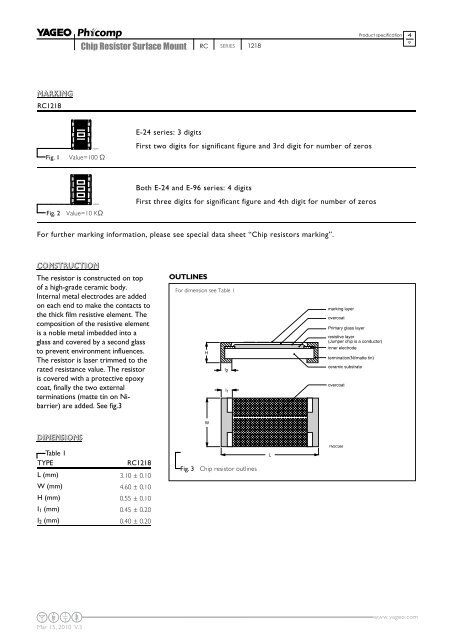
MARKING<br />
RC1218<br />
Mar 15, 2010 V.3<br />
Chip Resistor Surface Mount<br />
CONSTRUCTION<br />
The resistor is constructed on top<br />
of a high-grade ceramic body.<br />
Internal metal electrodes are added<br />
on each end to make the contacts to<br />
the thick film resistive element. The<br />
composition of the resistive element<br />
is a noble metal imbedded into a<br />
glass and covered by a second glass<br />
to prevent environment influences.<br />
The resistor is laser trimmed to the<br />
rated resistance value. The resistor<br />
is covered with a protective epoxy<br />
coat, finally the two external<br />
terminations (matte tin on Nibarrier)<br />
are added. See fig.3<br />
DIMENSIONS<br />
YNSC023<br />
Fig. 1 Value=100 Ω<br />
YNSC024<br />
Fig. 2 Value=10 KΩ<br />
Table 1<br />
TYPE RC1218<br />
L (mm) 3.10 ± 0.10<br />
W (mm) 4.60 ± 0.10<br />
H (mm) 0.55 ± 0.10<br />
I1 (mm) 0.45 ± 0.20<br />
I2 (mm) 0.40 ± 0.20<br />
RC SERIES 1218<br />
E-24 series: 3 digits<br />
First two digits for significant figure and 3rd digit for number of zeros<br />
Both E-24 and E-96 series: 4 digits<br />
First three digits for significant figure and 4th digit for number of zeros<br />
For further marking information, please see special data sheet “Chip resistors marking”.<br />
OUTLINES<br />
For dimension see Table 1<br />
H<br />
W<br />
Fig. 3 Chip resistor outlines<br />
I 2<br />
I 1<br />
L<br />
marking layer<br />
overcoat<br />
Product specification<br />
Primary glass layer<br />
resistive layer<br />
(Jumper chip is a conductor)<br />
inner electrode<br />
termination(Ni/matte tin)<br />
ceramic substrate<br />
overcoat<br />
YNSC066<br />
4<br />
9<br />
www.yageo.com