Electro Optical Characterisation of Short Wavelength Semiconductor ...
Electro Optical Characterisation of Short Wavelength Semiconductor ...
Electro Optical Characterisation of Short Wavelength Semiconductor ...

Create successful ePaper yourself
Turn your PDF publications into a flip-book with our unique Google optimized e-Paper software.
ZnSe Devices<br />
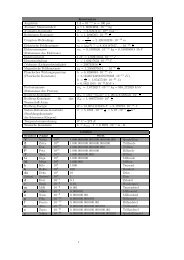
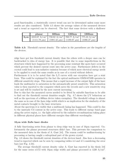
good functionality, a statistically correct trend can not be determined unless some more<br />
results are also considered. Table 4.5 shows the average values <strong>of</strong> the measured devices<br />
and a trend as expected can be observed. The fact that some devices with a shallower<br />
planar 600nm 1200nm 1800nm<br />
6µm 3310.67 A/cm 2 750.62 A/cm 2 769.77 A/cm 2 775.24 A/cm 2<br />
(1111.79 µm) (1081.42 µm) (1189.87 µm) (1086.27 µm)<br />
Table 4.3: Threshold current density. The values in the parentheses are the lengths <strong>of</strong><br />
the devices.<br />
ridge have got less threshold current density than the others with a deeper ones can be<br />
backtracked to idea <strong>of</strong> energy loss. It is possible that due to some imperfections in the<br />
structures which have happened by the processing some resistant like spots have occurred<br />
which prevent the desired current route into the active zone. Furthermore defects in the<br />
crystal could lead to non-radiative emission because <strong>of</strong> which more electrical energy needs<br />
to be applied to reach the same results as in case <strong>of</strong> a crystal without defects.<br />
Furthermore it is to be noted that the L/I curves with one exception have got a stair<br />
form. This could be explained by the fact the optical multimeter OMM-6710B operates in<br />
different sensitivity steps. This means that a rapid increase <strong>of</strong> the output light <strong>of</strong> the laser<br />
leads the multimeter to saturation in the automatically preset sensitivity. This saturation<br />
value is then reported to the computer which saves the records and a new sensitivity step<br />
is set and will be reached by the next current increasing.<br />
Due to this fact the measured curves needed to be fitted by suitable functions to be able<br />
to find out the threshold current densities sought. Fig. 4.7 shows the I/V behaviour as<br />
well as the spectrum <strong>of</strong> a 600nm device taken exemplary. The threshold voltage is almost<br />
the same as in case <strong>of</strong> the 2µm ridge width which is an implication for the similarity <strong>of</strong> the<br />
metal contacts brought to the laser structures.<br />
About the spectrum it is visible that a multimode lasing has happened. This could be due<br />
to the unsteady Cd content in the active zone. This leads to different energy band gaps<br />
along the active region, i.e. the light achieved by the radiative recombinations taking place<br />
in different physical places have different energies thus different wavelengths.<br />
10µm wide ZnSe laser diodes<br />
A fully functioning series from planar to deep ridge was in case <strong>of</strong> 10µm expected. Unfortunately<br />
the planar processed structures didn’t lase. This prevents the comparison to<br />
the measured data in the thesis <strong>of</strong> A. Gust [44]. The reason could be malfunctioning by<br />
processing or having caught a suboptimal part <strong>of</strong> the grown crystal.<br />
Fig. 4.8 shows the threshold current densities <strong>of</strong> the devices lased. Also here a decreasing<br />
trend is expected which can be seen by comparing tables 4.4 and 4.5 considering the error<br />
bars (see Fig. 4.10).<br />
The average threshold current density value A. Gust has reported in his thesis [44]<br />
for the same series s1172 with 10µm ridge width and planar processed is 1220 A/cm 2 .<br />
35