Electro Optical Characterisation of Short Wavelength Semiconductor ...
Electro Optical Characterisation of Short Wavelength Semiconductor ...
Electro Optical Characterisation of Short Wavelength Semiconductor ...

Create successful ePaper yourself
Turn your PDF publications into a flip-book with our unique Google optimized e-Paper software.
planar shallow ridge deep ridge<br />
2µm LED defect defect<br />
6µm lasing LED LED<br />
10µm LED lasing yellow light<br />
Table 4.6: Unmirrored GaN devices (g0975) measured in this thesis<br />
GaN Devices<br />
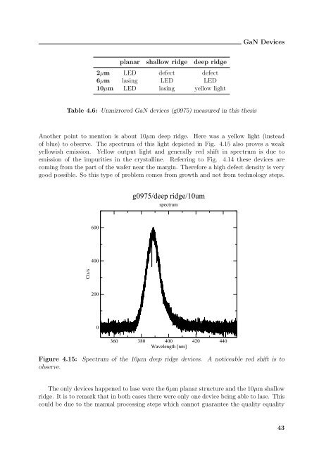
Another point to mention is about 10µm deep ridge. Here was a yellow light (instead<br />
<strong>of</strong> blue) to observe. The spectrum <strong>of</strong> this light depicted in Fig. 4.15 also proves a weak<br />
yellowish emission. Yellow output light and generally red shift in spectrum is due to<br />
emission <strong>of</strong> the impurities in the crystalline. Referring to Fig. 4.14 these devices are<br />
coming from the part <strong>of</strong> the wafer near the margin. Therefore a high defect density is very<br />
good possible. So this type <strong>of</strong> problem comes from growth and not from technology steps.<br />
Cts/s<br />
600<br />
400<br />
200<br />
0<br />
g0975/deep ridge/10um<br />
spectrum<br />
360 380 400 420 440<br />
<strong>Wavelength</strong> [nm]<br />
Figure 4.15: Spectrum <strong>of</strong> the 10µm deep ridge devices. A noticeable red shift is to<br />
observe.<br />
The only devices happened to lase were the 6µm planar structure and the 10µm shallow<br />
ridge. It is to remark that in both cases there were only one device being able to lase. This<br />
could be due to the manual processing steps which cannot guarantee the quality equality<br />
43