Electro Optical Characterisation of Short Wavelength Semiconductor ...
Electro Optical Characterisation of Short Wavelength Semiconductor ...
Electro Optical Characterisation of Short Wavelength Semiconductor ...

Create successful ePaper yourself
Turn your PDF publications into a flip-book with our unique Google optimized e-Paper software.
Data Analysis<br />
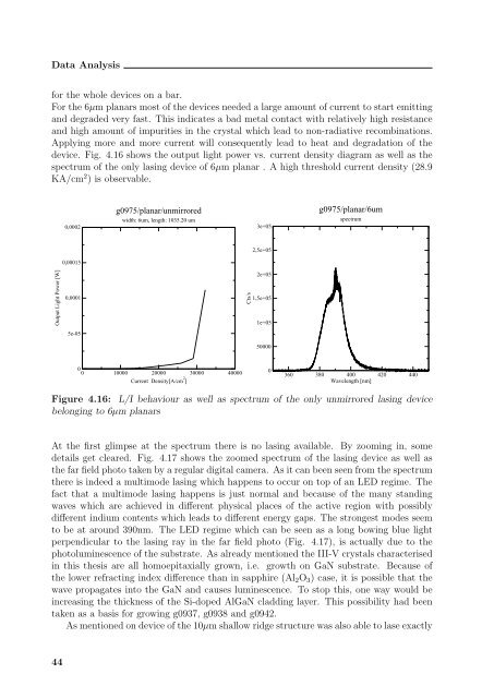
for the whole devices on a bar.<br />
For the 6µm planars most <strong>of</strong> the devices needed a large amount <strong>of</strong> current to start emitting<br />
and degraded very fast. This indicates a bad metal contact with relatively high resistance<br />
and high amount <strong>of</strong> impurities in the crystal which lead to non-radiative recombinations.<br />
Applying more and more current will consequently lead to heat and degradation <strong>of</strong> the<br />
device. Fig. 4.16 shows the output light power vs. current density diagram as well as the<br />
spectrum <strong>of</strong> the only lasing device <strong>of</strong> 6µm planar . A high threshold current density (28.9<br />
KA/cm 2 ) is observable.<br />
Output Light Power [W]<br />
0,0002<br />
0,00015<br />
0,0001<br />
5e-05<br />
g0975/planar/unmirrored<br />
width: 6um, length: 1035.20 um<br />
0 10000 20000<br />
Current Density[A/cm<br />
30000 40000<br />
2 0<br />
]<br />
Cts/s<br />
3e+05<br />
2,5e+05<br />
2e+05<br />
1,5e+05<br />
1e+05<br />
50000<br />
0<br />
g0975/planar/6um<br />
spectrum<br />
360 380 400 420 440<br />
<strong>Wavelength</strong> [nm]<br />
Figure 4.16: L/I behaviour as well as spectrum <strong>of</strong> the only unmirrored lasing device<br />
belonging to 6µm planars<br />
At the first glimpse at the spectrum there is no lasing available. By zooming in, some<br />
details get cleared. Fig. 4.17 shows the zoomed spectrum <strong>of</strong> the lasing device as well as<br />
the far field photo taken by a regular digital camera. As it can been seen from the spectrum<br />
there is indeed a multimode lasing which happens to occur on top <strong>of</strong> an LED regime. The<br />
fact that a multimode lasing happens is just normal and because <strong>of</strong> the many standing<br />
waves which are achieved in different physical places <strong>of</strong> the active region with possibly<br />
different indium contents which leads to different energy gaps. The strongest modes seem<br />
to be at around 390nm. The LED regime which can be seen as a long bowing blue light<br />
perpendicular to the lasing ray in the far field photo (Fig. 4.17), is actually due to the<br />
photoluminescence <strong>of</strong> the substrate. As already mentioned the III-V crystals characterised<br />
in this thesis are all homoepitaxially grown, i.e. growth on GaN substrate. Because <strong>of</strong><br />
the lower refracting index difference than in sapphire (Al2O3) case, it is possible that the<br />
wave propagates into the GaN and causes luminescence. To stop this, one way would be<br />
increasing the thickness <strong>of</strong> the Si-doped AlGaN cladding layer. This possibility had been<br />
taken as a basis for growing g0937, g0938 and g0942.<br />
As mentioned on device <strong>of</strong> the 10µm shallow ridge structure was also able to lase exactly<br />
44