Electro Optical Characterisation of Short Wavelength Semiconductor ...
Electro Optical Characterisation of Short Wavelength Semiconductor ...
Electro Optical Characterisation of Short Wavelength Semiconductor ...

Create successful ePaper yourself
Turn your PDF publications into a flip-book with our unique Google optimized e-Paper software.
GaN Devices<br />
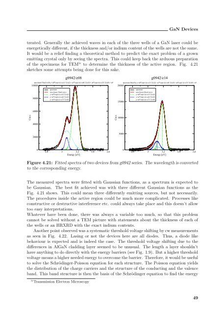
treated. Generally the achieved waves in each <strong>of</strong> the three wells <strong>of</strong> a GaN laser could be<br />
energetically different, if the thickness and/or indium content <strong>of</strong> the wells are not the same.<br />
It would be a relief finding a theoretical method to predict the exact problem <strong>of</strong> a grown<br />
emitting crystal only by seeing the spectra. This could keep back the arduous preparation<br />
<strong>of</strong> the specimens for TEM iv to determine the thickness <strong>of</strong> the active region. Fig. 4.21<br />
sketches some attempts being done for this sake.<br />
Cts/s<br />
spectrum fitted with y=a0*exp(-((x-a1)^2)/a2) +a3*exp(-((x-a4)^2)/a5)+ a6*exp(-((x-a7)^2)/a8) +a9<br />
10000<br />
8000<br />
6000<br />
4000<br />
2000<br />
0<br />
spectrum<br />
non-linear fitted curve<br />
y=a0*exp(-((x-a1)^2)/a2)<br />
y=a3*exp(-((x-a4)^2)/a5)<br />
y=a6*exp(-((x-a7)^2)/a8)<br />
g0942/e08<br />
2,8 3 3,2 3,4 3,6<br />
Energy [eV]<br />
Cts/s<br />
spectrum fitted by y=a0*exp(-((x-a1)^2)/a2) +a3*exp(-((x-a4)^2)/a5)+ a6*exp(-((x-a7)^2)/a8) +a9<br />
20000<br />
15000<br />
10000<br />
5000<br />
0<br />
spectrum<br />
non-linear fitted curve<br />
y=a0*exp(-((x-a1)^2)/a2)<br />
y=a3*exp(-((x-a4)^2)/a5)<br />
y=a6*exp(-((x-a7)^2)/a8)<br />
g0942/e14<br />
2,8 3 3,2 3,4 3,6<br />
Energy [eV]<br />
Figure 4.21: Fitted spectra <strong>of</strong> two devices from g0942 series. The wavelength is converted<br />
to the corresponding energy.<br />
The measured spectra were fitted with Gaussian functions, as a spectrum is expected to<br />
be Gaussian. The best fit achieved was with three different Gaussian functions as the<br />
Fig. 4.21 shows. This could mean three differently emitting sources, but not necessarily.<br />
The procedures inside the active region could be much more complicated. Processes like<br />
constructive or destructive interference etc. could always take place and this doesn’t allow<br />
too easy interpretations.<br />
Whatever have been done, there was always a variable too much, so that this problem<br />
cannot be solved without a TEM picture with statements about the thickness <strong>of</strong> each <strong>of</strong><br />
the wells or an HRXRD with the exact indium contents.<br />
Another point observed was a systematic threshold voltage shifting by cw measurements<br />
as seen in Fig. 4.22. Lasing or not the devices here are all diodes. Thus, a diode like<br />
behaviour is expected and is indeed the case. The threshold voltage shifting due to the<br />
differences in AlGaN cladding layer seemed to be unusual. The length a layer shouldn’t<br />
have anything to do directly with the energy barriers (see Fig. 1.9). But a higher threshold<br />
voltage means a higher needed energy to overcome the barrier. Therefore, it would be useful<br />
to solve the Schrödinger-Poisson equation for each structure. The Poisson equation yields<br />
the distribution <strong>of</strong> the charge carriers and the structure <strong>of</strong> the conducting and the valence<br />
band. This band structure is then the basis <strong>of</strong> the Schrödinger equation to find the energy<br />
iv Transmission <strong>Electro</strong>n Microscopy<br />
49