Modeling And Analysis Of Buck-Boost DC/DC Pulse Converter XII ...
Modeling And Analysis Of Buck-Boost DC/DC Pulse Converter XII ...
Modeling And Analysis Of Buck-Boost DC/DC Pulse Converter XII ...

Create successful ePaper yourself
Turn your PDF publications into a flip-book with our unique Google optimized e-Paper software.
⎛ 1 1 ⎞<br />
I ⎜<br />
⎟<br />
L min =<br />
⎜<br />
− kU d<br />
( k)<br />
R Lf ⎟<br />
, (15)<br />
2<br />
⎝ 1−<br />
2 ⎠<br />
- in the mode of operation with discontinuous<br />
inductance current<br />
I 0 . (16)<br />
L min =<br />
The boundary value of inductance resulting from<br />
the condition of continuity of the inductance<br />
current:<br />
( 1−<br />
k )<br />
Lmin<br />
=<br />
2 f<br />
R<br />
. (17)<br />
The continuity of the diode current<br />
L ≥ L .<br />
The ripple coefficient of the output voltage:<br />
for min<br />
U 0 r<br />
U 0<br />
∆<br />
= (18)<br />
- in the mode of operation with continuous<br />
inductance current<br />
k<br />
r = , (19)<br />
RCf<br />
- in the mode of operation with discontinuous<br />
inductance current<br />
2<br />
( k R − fL)<br />
1<br />
r = . (20)<br />
2 2<br />
2Lf<br />
R C<br />
The analysis of mathematical relationships shows<br />
several important characteristics of the converter<br />
under consideration. In the expression (4) describing<br />
the relationship between the input voltage and the<br />
output appears a k factor responsible for lowering<br />
1<br />
the voltage and the factor responsible for<br />
1−<br />
k<br />
increasing the voltage. Analogously, you can<br />
compose expression defining the relationship<br />
between the output and input current [6]. The<br />
continuity of the current in the inductance depends<br />
on: the value of inductance, the input voltage, the fill<br />
factor, the load and the PWM modulation frequency.<br />
The operating mode shown in Figure 2 in c), occurs<br />
when the inductance current reaches a value of zero<br />
during the modulation.<br />
The relative diode conduction time, can be<br />
determined according to the relation (3). The voltage<br />
ripple factor determines the quality of the output<br />
voltage regulation.<br />
2<br />
140<br />
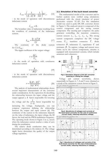
2.2. Simulation of the buck-boost converter<br />
The mathematical model of the converter and its<br />
further analysis were verified using simulations<br />
performed with the circuit simulator of power<br />
electronics systems TCAD. For this simulation<br />
model was used to pulse <strong>DC</strong>/<strong>DC</strong> converter shown<br />
in Figure 5. The analyzed circuit is composed of the<br />
control component and the strong current<br />
component. The steering part comprises: the pulse<br />
generator controlling the transistor connector,<br />
current sensors: i T , i D , i L , i C , i R . The strong<br />
current component comprises: the <strong>DC</strong> voltage<br />
source U d , transistor connector T , diode<br />
connector D , inductance L , capacitance C and<br />
resistance R . To register, voltage and current wave<br />
forms on/in the various components, circuitry is<br />
equipped with measurement systems, which include<br />
ammeters and voltmeters.<br />
Fig.5. Simulation diagram of <strong>DC</strong>/<strong>DC</strong> converter<br />
lowering or raising the voltage.<br />
Voltage and current waveforms, shown<br />
sequentially in Figures 6, 7, 8 and 9 were obtained as<br />
a result of the simulation system shown in Figure 5.<br />
i T<br />
i L<br />
i D<br />
i C<br />
Fig.6. Waveforms of voltages and currents of<br />
the buck-boost converter for the case of continuous<br />
current mode, reducing inductance voltage.<br />
i L<br />
i T<br />
i R<br />
i R<br />
i D<br />
i C<br />
U 0<br />
u L<br />
u L<br />
U 0<br />
Fig.7. Waveforms of voltages and currents of the<br />
buck-boost converter for the case of discontinuous<br />
current mode, reducing inductance in voltage.<br />
U d<br />
U d<br />
u T<br />
u T<br />
u<br />
D<br />
u D