PCISA-8450 User Manual - iEi
PCISA-8450 User Manual - iEi
PCISA-8450 User Manual - iEi

Create successful ePaper yourself
Turn your PDF publications into a flip-book with our unique Google optimized e-Paper software.
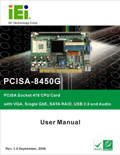
<strong>PCISA</strong>-<strong>8450</strong>G CPU Card<br />
0-1<br />
1
REVISION HISTORY<br />
Title<br />
<strong>PCISA</strong>-<strong>8450</strong>G Intel® Pentium® 4/ Celeron® D CPU Card<br />
Revision Number Description Date of Issue<br />
1.0 Initial release September 2006<br />
COPYRIGHT NOTICE<br />
The information in this document is subject to change without prior notice in order to<br />
improve reliability, design and function and does not represent a commitment on the part of<br />
the manufacturer.<br />
In no event will the manufacturer be liable for direct, indirect, special, incidental, or<br />
consequential damages arising out of the use or inability to use the product or<br />
documentation, even if advised of the possibility of such damages.<br />
This document contains proprietary information protected by copyright. All rights are<br />
reserved. No part of this manual may be reproduced by any mechanical, electronic, or<br />
other means in any form without prior written permission of the manufacturer.<br />
TRADEMARKS<br />
IBM PC is a registered trademark of International Business Machines Corporation. INTEL<br />
is a registered trademark of INTEL Corporation. AMI is registered trademarks of American<br />
Megatrends Inc. Other product names mentioned herein are used for identification<br />
purposes only and may be trademarks and/or registered trademarks of their respective<br />
owners.<br />
2 IEI ® Technology, Corp.
<strong>PCISA</strong>-<strong>8450</strong>G CPU Card<br />
Table of Contents<br />
1 INTRODUCTION................................................................................................... 15<br />
1.1 <strong>PCISA</strong>-<strong>8450</strong>G CPU CARD OVERVIEW.............................................................. 16<br />
1.1.1 <strong>PCISA</strong>-<strong>8450</strong>G CPU Card Applications ........................................................... 16<br />
1.1.2 <strong>PCISA</strong>-<strong>8450</strong>G CPU Card Benefits .................................................................. 16<br />
1.1.3 <strong>PCISA</strong>-<strong>8450</strong>G CPU Card Features ................................................................. 16<br />
1.2 <strong>PCISA</strong>-<strong>8450</strong>G CPU CARD OVERVIEW.............................................................. 17<br />
1.2.1 <strong>PCISA</strong>-<strong>8450</strong>G CPU Card Connectors............................................................. 18<br />
1.2.2 Technical Specifications: ................................................................................. 19<br />
2 DETAILED SPECIFICATIONS ........................................................................... 21<br />
2.1 COMPATIBLE IEI BACKPLANES .......................................................................... 22<br />
2.2 CPU SUPPORT.................................................................................................... 22<br />
2.2.1 Intel® Pentium® 4........................................................................................... 22<br />
2.2.2 Intel® Celeron® D........................................................................................... 22<br />
2.3 ONBOARD CHIPSETS .......................................................................................... 23<br />
2.3.1 Northbridge and Southbridge Chipsets ........................................................... 23<br />
2.3.2 845GV Northbridge Chipset ............................................................................ 23<br />
2.3.3 ICH4 Southbridge Chipset............................................................................... 24<br />
2.4 DATA FLOW........................................................................................................ 25<br />
2.5 GRAPHICS SUPPORT ........................................................................................... 26<br />
2.6 MEMORY SUPPORT............................................................................................. 28<br />
2.7 PCI BUS INTERFACE SUPPORT ........................................................................... 28<br />
2.8 GBE ETHERNET ................................................................................................. 28<br />
2.9 DRIVE INTERFACES ............................................................................................ 29<br />
2.9.1 SATA Drives ..................................................................................................... 29<br />
2.9.2 IDE HDD Interfaces ........................................................................................ 29<br />
2.9.3 Floppy Disk Drive (FDD)................................................................................ 30<br />
2.10 SERIAL PORTS .................................................................................................... 30<br />
2.11 REAL TIME CLOCK............................................................................................. 30<br />
2.12 SYSTEM MONITORING........................................................................................ 30<br />
2.13 INFRARED DATA ASSOCIATION (IRDA) INTERFACE............................................ 30<br />
2.14 USB INTERFACES............................................................................................... 31<br />
0-33
2.15 BIOS ................................................................................................................. 31<br />
2.16 OPERATING TEMPERATURE AND TEMPERATURE CONTROL................................. 31<br />
2.17 AUDIO CODEC.................................................................................................... 31<br />
2.18 POWER CONSUMPTION....................................................................................... 33<br />
2.19 PACKAGED CONTENTS AND OPTIONAL ACCESSORY ITEMS................................. 33<br />
2.19.1 Package Contents........................................................................................... 33<br />
2.19.2 Optional Accessory Items............................................................................... 34<br />
3 CONNECTORS AND JUMPERS ......................................................................... 35<br />
3.1 PERIPHERAL INTERFACE CONNECTORS .............................................................. 36<br />
3.1.1 <strong>PCISA</strong>-<strong>8450</strong>G CPU Card Layout .................................................................... 36<br />
3.1.2 Peripheral Interface Connectors ..................................................................... 37<br />
3.1.3 Rear Panel Connectors.................................................................................... 38<br />
3.1.4 Onboard Jumpers............................................................................................. 38<br />
3.2 INTERNAL PERIPHERAL CONNECTORS................................................................ 39<br />
3.2.1 8 Bit GPIO Connector ..................................................................................... 39<br />
3.2.2 ATX-12V Power Source Connector.................................................................. 40<br />
3.2.3 Backplane to Mainboard ATX Connector........................................................ 41<br />
3.2.4 Compact Flash Connector ............................................................................... 42<br />
3.2.5 CPU Cooling Fan Connector .......................................................................... 44<br />
3.2.6 FDD Connector ............................................................................................... 45<br />
3.2.7 Front Panel Connector .................................................................................... 47<br />
3.2.8 IDE Interface Connectors................................................................................ 49<br />
3.2.9 IrDA Connector................................................................................................ 50<br />
3.2.10 Keyboard Connector ...................................................................................... 51<br />
3.2.11 Line In Connector........................................................................................... 53<br />
3.2.12 Mic In Connector ........................................................................................... 54<br />
3.2.13 Parallel Port Connector ................................................................................ 55<br />
3.2.14 Power Switch Button...................................................................................... 56<br />
3.2.15 SATA Drive Ports ........................................................................................... 57<br />
3.2.16 Serial Communications Connector................................................................ 59<br />
3.2.17 SMI Switch Connector ................................................................................... 60<br />
3.2.18 Internal USB Connectors............................................................................... 61<br />
3.3 EXTERNAL (REAR PANEL) CONNECTORS ........................................................... 63<br />
3.3.1 Keyboard/Mouse Connector ............................................................................ 63<br />
3.3.2 USB Connectors............................................................................................... 64<br />
4 IEI ® Technology, Corp.
<strong>PCISA</strong>-<strong>8450</strong>G CPU Card<br />
3.3.3 Ethernet Connector.......................................................................................... 64<br />
3.3.4 VGA Connector ................................................................................................ 66<br />
3.3.5 Audio Line Out Connector ............................................................................... 67<br />
3.4 ONBOARD JUMPERS ........................................................................................... 67<br />
3.4.1 CF Card Setup Jumper .................................................................................... 68<br />
3.4.2 Reset CMOS Jumper........................................................................................ 69<br />
4 INSTALLATION AND CONFIGURATION ....................................................... 71<br />
4.1 INSTALLATION CONSIDERATIONS ....................................................................... 72<br />
4.1.1 Installation Notices .......................................................................................... 72<br />
4.2 UNPACKING........................................................................................................ 73<br />
4.2.1 Unpacking Precautions.................................................................................... 73<br />
4.2.2 Checklist........................................................................................................... 74<br />
4.3 <strong>PCISA</strong>-<strong>8450</strong>G CPU CARD INSTALLATION ........................................................ 74<br />
4.3.1 CPU Installation .............................................................................................. 75<br />
4.3.2 Optional Cooling Kit (CF-521-RS) Installation .............................................. 76<br />
4.3.3 DIMM Module Installation.............................................................................. 78<br />
4.3.3.1 Purchasing the Memory Module............................................................... 78<br />
4.3.3.2 DIMM Module Installation....................................................................... 78<br />
4.3.4 Peripheral Device Connection......................................................................... 80<br />
4.3.4.1 IDE Disk Drive Connector (IDE1) ........................................................... 80<br />
4.4 JUMPER CONFIGURATION ................................................................................... 81<br />
4.5 CHASSIS INSTALLATION ..................................................................................... 81<br />
4.6 REAR PANEL CONNECTORS ................................................................................ 81<br />
4.6.1 PS/2 Connection............................................................................................... 81<br />
4.6.2 USB Connection............................................................................................... 82<br />
4.6.3 Ethernet Connection ........................................................................................ 82<br />
4.6.4 VGA Connection .............................................................................................. 82<br />
4.6.5 Line Out Connection........................................................................................ 82<br />
5 AMI BIOS SETUP.................................................................................................. 83<br />
5.1 INTRODUCTION .................................................................................................. 84<br />
5.1.1 Starting Setup................................................................................................... 84<br />
5.1.2 Using Setup ...................................................................................................... 84<br />
5.1.3 Getting Help..................................................................................................... 85<br />
5.1.4 Unable to Reboot After Configuration Changes.............................................. 85<br />
5.1.5 BIOS Main Menu ............................................................................................. 85<br />
0-55
5.2 STANDARD CMOS SETUP.................................................................................. 88<br />
5.3 ADVANCED CMOS SETUP ................................................................................. 94<br />
5.4 ADVANCED CHIPSET SETUP.............................................................................. 103<br />
5.5 POWER MANAGEMENT SETUP.......................................................................... 109<br />
5.6 PCI / PLUG AND PLAY SETUP............................................................................119<br />
5.7 PERIPHERAL SETUP .......................................................................................... 122<br />
5.8 HARDWARE MONITOR SETUP........................................................................... 127<br />
5.9 AUTO-DETECT HARD DISKS ............................................................................ 128<br />
6 SOFTWARE DRIVERS ....................................................................................... 129<br />
6.1 AVAILABLE SOFTWARE DRIVERS...................................................................... 130<br />
6.2 CHIPSET DRIVER INSTALLATION....................................................................... 131<br />
6.3 INTEL® APPLICATION ACCELERATOR INSTALLATION....................................... 135<br />
6.4 INTEL® GRAPHICS MEDIA ACCELERATOR DRIVER .......................................... 136<br />
6.5 REALTEK LAN DRIVER (FOR GBE LAN) INSTALLATION................................. 140<br />
6.6 REALTEK AUDIO DRIVER INSTALLATION ......................................................... 143<br />
6.7 ALI SATA/RAID DRIVER ............................................................................... 146<br />
A BIOS CONFIGURATION OPTIONS ................................................................ 149<br />
A.1 BIOS CONFIGURATION OPTIONS ..................................................................... 150<br />
B WATCHDOG TIMER .......................................................................................... 155<br />
C ADDRESS MAPPING.......................................................................................... 159<br />
C.1 I/O ADDRESS MAP ........................................................................................... 160<br />
C.2 1 ST MB MEMORY ADDRESS MAP ..................................................................... 160<br />
C.3 IRQ MAPPING TABLE....................................................................................... 161<br />
C.4 DMA CHANNEL ASSIGNMENTS ....................................................................... 161<br />
D EXTERNAL AC’97 AUDIO CODEC ................................................................. 163<br />
D.1 INTRODUCTION ................................................................................................ 164<br />
D.2 DRIVER INSTALLATION..................................................................................... 164<br />
D.3 SOUND EFFECT CONFIGURATION ..................................................................... 165<br />
D.4 SOUND EFFECT ................................................................................................ 166<br />
D.5 ENVIRONMENT SIMULATION ............................................................................ 166<br />
D.6 KARAOKE MODE.............................................................................................. 167<br />
D.7 EQUALIZER SELECTION.................................................................................... 168<br />
D.8 SPEAKER CONFIGURATION............................................................................... 169<br />
6 IEI ® Technology, Corp.
<strong>PCISA</strong>-<strong>8450</strong>G CPU Card<br />
D.9 SPEAKER TEST ................................................................................................. 170<br />
D.10 S/PDIF-IN & S/PDIF-OUT .............................................................................. 171<br />
D.11 CONNECTOR SENSING ...................................................................................... 171<br />
D.12 HRTF DEMO.................................................................................................... 173<br />
D.13 MICROPHONE EFFECT ...................................................................................... 173<br />
D.14 GENERAL ......................................................................................................... 173<br />
E ALI ® RAID FOR SATA........................................................................................ 175<br />
E.1 INTRODUCTION ................................................................................................ 176<br />
E.1.1 Precautions ............................................................................................. 176<br />
E.2 FEATURES AND BENEFITS................................................................................. 177<br />
E.3 ACCESSING THE ALI RAID UTILITY................................................................ 177<br />
E.4 RAID OPTIONS:............................................................................................... 179<br />
E.4.1 Create RAID 0 Striping for Performance ............................................... 179<br />
E.4.2 Create RAID 1 Mirroring for Reliability ................................................ 181<br />
E.4.3 Create JBOD for Integrated Capacity .................................................... 182<br />
E.4.4 Stripe Size................................................................................................ 184<br />
E.4.5 Delete RAID Setting & Partition ............................................................ 184<br />
E.4.6 Delete All RAID Setting & Partition....................................................... 185<br />
E.4.7 Rebuild RAID Array................................................................................ 185<br />
E.4.8 Select Boot Drive .................................................................................... 186<br />
INDEX.................................................................................................................... 187<br />
0-77
List of Figures<br />
Figure 1-1 <strong>PCISA</strong>-<strong>8450</strong>G CPU Card Overview (Front Side) .....................................17<br />
Figure 1-2 <strong>PCISA</strong>-<strong>8450</strong>G CPU Card Overview (Solder Side) ...................................17<br />
Figure 2-1: Data Flow Block Diagram........................................................................25<br />
Figure 3-1: Connector and Jumper Locations (Front Side)....................................36<br />
Figure 3-2: Connector and Jumper Locations (Solder Side)..................................37<br />
Figure 3-3: CN5 Connector Location.........................................................................40<br />
Figure 3-4: PW1 Connector Location........................................................................41<br />
Figure 3-5: CN8 Connector Location.........................................................................42<br />
Figure 3-6: CF1 Connector Location.........................................................................44<br />
Figure 3-7 FAN1 Connector Location........................................................................45<br />
Figure 3-8: FDD Connector Location ........................................................................47<br />
Figure 3-9: CN6 Connector Location.........................................................................48<br />
Figure 3-10: IDE Interface Connector Locations......................................................50<br />
Figure 3-11: IrDA Connector Location ......................................................................51<br />
Figure 3-12: CN9 Connector Location.......................................................................52<br />
Figure 3-13: CN1 Connector Location.......................................................................53<br />
Figure 3-14: CN2 Connector Location.......................................................................54<br />
Figure 3-15: LPT1 Connector Location.....................................................................56<br />
Figure 3-16: CN4 Connector Locations.....................................................................57<br />
Figure 3-17: SATA Connector Locations..................................................................58<br />
Figure 3-18 COM1, COM2 Connector Location ........................................................60<br />
Figure 3-19: CN3 Connector Location.......................................................................61<br />
Figure 3-20: USB1 Connector Locations ..................................................................62<br />
Figure 3-21: <strong>PCISA</strong>-<strong>8450</strong>G CPU Card Rear Panel ....................................................63<br />
Figure 3-22: KB/MS1 Pinout locations ......................................................................64<br />
Figure 3-23: LAN1 Connector ....................................................................................65<br />
Figure 3-24: VGA1 Connector ....................................................................................66<br />
Figure 3-25: Jumper Locations..................................................................................67<br />
Figure 3-26: Jumper Locations..................................................................................68<br />
8 IEI ® Technology, Corp.
<strong>PCISA</strong>-<strong>8450</strong>G CPU Card<br />
Figure 4-1: Locking the CPU into the CPU Socket ..................................................76<br />
Figure 4-2: IEI CF-521-RS Cooling Kit.......................................................................76<br />
Figure 4-3: Securing the Cooling Kit.........................................................................77<br />
Figure 4-4: Connect the Cooling Fan Cable .............................................................78<br />
Figure 4-5: Installing the DIMM Module ....................................................................79<br />
Figure 4-6: Locking the DIMM Module ......................................................................79<br />
Figure 6-1: Chipset Software Installation Utility Extracting Files ....................... 131<br />
Figure 6-2: InstallShield Wizard Preparation Screen............................................ 131<br />
Figure 6-3: Chipset Software Installation Utility Welcome Screen ..................... 132<br />
Figure 6-4: Chipset Software Installation Utility License Agreement................. 132<br />
Figure 6-5: Chipset Software Installation Utility Readme File Information........ 133<br />
Figure 6-6: Installing Chipset Driver ...................................................................... 133<br />
Figure 6-7: Chipset Software Installation Utility Complete.................................. 134<br />
Figure 6-8: Intel® Chipset Graphics Driver Software InstallShield Wizard........ 136<br />
Figure 6-9: InstallShield Wizard Extracting Files.................................................. 137<br />
Figure 6-10: Intel® Graphics Media Accelerator Driver Welcome Screen ......... 137<br />
Figure 6-11: Intel® Graphics Media Accelerator Driver License Agreement ..... 138<br />
Figure 6-12: Intel® Graphics Media Accelerator Driver Installing Notice........... 138<br />
Figure 6-13: Intel® Graphics Media Accelerator Installation Complete ............. 139<br />
Figure 6-14: Realtek LAN Driver InstallShield Wizard.......................................... 140<br />
Figure 6-15: Realtek LAN Driver Welcome ............................................................ 141<br />
Figure 6-16: Realtek LAN Driver Ready to Install ................................................. 141<br />
Figure 6-17: Realtek LAN Driver Setup Status ...................................................... 142<br />
Figure 6-18: Realtek LAN Driver Installation Complete........................................ 142<br />
Figure 6-19: InstallShield Wizard Extracting Files................................................ 143<br />
Figure 6-20: Audio Driver Install Shield Wizard Starting ..................................... 143<br />
Figure 6-21: Audio Driver Setup Preparation ........................................................ 144<br />
Figure 6-22: Audio Driver Digital Signal ................................................................ 144<br />
Figure 6-23: Audio Driver Installation Continues ................................................. 145<br />
Figure 6-24: Audio Driver Installation Complete................................................... 145<br />
Figure 6-25: RAID Driver Preparing Setup Screen................................................ 146<br />
Figure 6-26: RAID Driver Install Wizard Welcome Screen ................................... 146<br />
Figure 6-27: RAID Driver Installing Screen............................................................ 147<br />
0-99
Figure 6-28: RAID Driver Digital Signal.................................................................. 148<br />
Figure 6-29: InstallShield Wizard Complete Screen ............................................. 148<br />
Figure 6-30: Accessing ALi RAID BIOS Utility ...................................................... 178<br />
Figure 6-31: RAID BIOS Setup Utility ..................................................................... 179<br />
10 IEI ® Technology, Corp.
<strong>PCISA</strong>-<strong>8450</strong>G CPU Card<br />
List of Tables<br />
Table 1-1: Technical Specifications ..........................................................................19<br />
Table 2-1: Supported CPUs........................................................................................22<br />
Table 2-2: Supported Celeron® D CPUs ...................................................................23<br />
Table 2-3: Power Consumption .................................................................................33<br />
Table 3-1: Peripheral Interface Connectors..............................................................38<br />
Table 3-2: Peripheral Interface Connectors..............................................................38<br />
Table 3-3: Onboard Jumpers .....................................................................................39<br />
Table 3-4: CN5 Connector Pinouts............................................................................39<br />
Table 3-5: PW1 Connector Pinouts ...........................................................................40<br />
Table 3-6: CN8 Connector Pinouts............................................................................42<br />
Table 3-7: CF1 Connector Pinouts ............................................................................43<br />
Table 3-8 FAN1 Connector Pinouts...........................................................................44<br />
Table 3-9: FDD Connector Pinouts............................................................................46<br />
Table 3-10: CN6 Connector Pinouts..........................................................................48<br />
Table 3-11: IDE Interface Connector Pinouts ...........................................................49<br />
Table 3-12: IrDA Connector Pinouts..........................................................................51<br />
Table 3-13: CN9 Connector Pinouts..........................................................................52<br />
Table 3-14: CN1 Connector Pin Outs ........................................................................53<br />
Table 3-15: CN2 Connector Pin Outs ........................................................................54<br />
Table 3-16: LPT1 Connector Pinouts ........................................................................55<br />
Table 3-17: CN4 Connector Pinouts..........................................................................56<br />
Table 3-18: SATA Connector Pinouts .......................................................................58<br />
Table 3-19: COM1, COM2 Connector Pinouts ..........................................................59<br />
Table 3-20: CN3Connector Pinouts...........................................................................61<br />
Table 3-21: USB1 Connector Pinouts........................................................................62<br />
Table 3-22: KB/MS1 Pinouts.......................................................................................64<br />
Table 3-23: USB3, USB2 Connector Pinouts............................................................64<br />
Table 3-24: LAN1 Connector Pinouts........................................................................65<br />
Table 3-25: LAN1 Connector LEDs............................................................................65<br />
0-11
Table 3-26: VGA1 Connector Pinouts .......................................................................66<br />
Table 3-27: CN7 Connector Pinouts..........................................................................67<br />
Table 3-28: CF Card Setup Jumper Settings ............................................................69<br />
Table 3-29: Reset CMOS Jumper Settings ...............................................................69<br />
Table 4-1: IEI Provided Cables...................................................................................80<br />
Table 5-1: BIOS Navigation Keys...............................................................................84<br />
12 IEI ® Technology, Corp.
<strong>PCISA</strong>-<strong>8450</strong>G CPU Card<br />
List of BIOS Menus<br />
BIOS Menu 1: BIOS Main Menu .................................................................................85<br />
BIOS Menu 2: Standard CMOS Setup Menu.............................................................88<br />
BIOS Menu 3: Advanced CMOS Setup Menu ...........................................................94<br />
BIOS Menu 4: Advanced CMOS Setup Menu ........................................................ 103<br />
BIOS Menu 5: Power Management Setup Menu ................................................... 109<br />
BIOS Menu 6: PCI / Plug and Play Setup Menu..................................................... 119<br />
BIOS Menu 7: Peripheral Setup Menu.................................................................... 122<br />
BIOS Menu 8: Hardware Monitor Setup Menu....................................................... 127<br />
0-13
Glossary<br />
AC ’97 Audio Codec 97<br />
ACPI Advanced Configuration and<br />
Power Interface<br />
APM Advanced Power Management<br />
ARMD ATAPI Removable Media Device<br />
ASKIR Shift Keyed Infrared<br />
ATA Advanced Technology<br />
Attachments<br />
BIOS Basic Input/Output System<br />
CFII Compact Flash Type 2<br />
CMOS Complementary Metal Oxide<br />
Semiconductor<br />
CPU Central Processing Unit<br />
Codec Compressor/Decompressor<br />
COM Serial Port<br />
DAC Digital to Analog Converter<br />
DDR Double Data Rate<br />
DIMM Dual Inline Memory Module<br />
DIO Digital Input/Output<br />
DMA Direct Memory Access<br />
EIDE Enhanced IDE<br />
EIST Enhanced Intel SpeedStep<br />
Technology<br />
FDD Floppy Disk Drive<br />
FDC Floppy Disk Connector<br />
FFIO Flexible File Input/Output<br />
FIFO First In/First Out<br />
FSB Front Side Bus<br />
IrDA Infrared Data Association<br />
HDD Hard Disk Drive<br />
IDE Integrated Data Electronics<br />
I/O Input/Output<br />
ICH4 I/O Controller Hub 4<br />
L1 Cache Level 1 Cache<br />
L2 Cache Level 2 Cache<br />
LCD Liquid Crystal Display<br />
LPT Parallel Port Connector<br />
LVDS Low Voltage Differential Signaling<br />
MAC Media Access Controller<br />
OS Operating System<br />
PCI Peripheral Connect Interface<br />
PIO Programmed Input Output<br />
PnP Plug and Play<br />
POST Power On Self Test<br />
RAM Random Access Memory<br />
SATA Serial ATA<br />
S.M.A.R.T Self Monitoring Analysis and<br />
Reporting Technology<br />
SPD Serial Presence Detect<br />
S/PDI Sony/Philips Digital Interface<br />
SDRAM Synchronous Dynamic Random<br />
Access Memory<br />
SIR Serial Infrared<br />
UART Universal Asynchronous<br />
Receiver-transmitter<br />
USB Universal Serial Bus<br />
VGA Video Graphics Adapter<br />
14 IEI ® Technology, Corp.
<strong>PCISA</strong>-<strong>8450</strong>G CPU Card<br />
Chapter<br />
1<br />
1<br />
Introduction<br />
1-15 15
1.1 <strong>PCISA</strong>-<strong>8450</strong>G CPU Card Overview<br />
The PICMG 1.0 form factor <strong>PCISA</strong>-<strong>8450</strong>G Intel® Pentium® CPU platform is fully equipped<br />
with a high performance processor and advanced multi-mode I/Os. The <strong>PCISA</strong>-<strong>8450</strong>G is<br />
designed for system manufacturers, integrators, and VARs that want performance,<br />
reliability, and quality at a reasonable price.<br />
1.1.1 <strong>PCISA</strong>-<strong>8450</strong>G CPU Card Applications<br />
The <strong>PCISA</strong>-<strong>8450</strong>G CPU card is designed for use in industrial applications where board<br />
expansion is critical and operational reliability is essential.<br />
1.1.2 <strong>PCISA</strong>-<strong>8450</strong>G CPU Card Benefits<br />
Some of the <strong>PCISA</strong>-<strong>8450</strong>G CPU card benefits include,<br />
• providing access to multiple PCI and ISA expansion slots for easy system<br />
expansion<br />
• operating reliably in harsh industrial environments with ambient<br />
temperatures as high as 60°C<br />
• rebooting automatically if the BIOS watchdog timer detects that the<br />
system is no longer operating<br />
1.1.3 <strong>PCISA</strong>-<strong>8450</strong>G CPU Card Features<br />
Some of the <strong>PCISA</strong>-<strong>8450</strong>G CPU card features are listed below:<br />
• Complies with PICMG 1.0<br />
• Complies with RoHS<br />
• Supports Socket 478 Intel® Pentium® 4/Intel® Celeron® D CPUs<br />
• Supports a maximum front side bus (FSB) speed up to 533MHz<br />
• Supports up to 1GB of 333MHz single channel DDR memory<br />
• Comes with one high performance gigabit Ethernet (GbE) controller<br />
• Supports two SATA channels with transfer rates up to 1.5Gb/s<br />
• Supports four USB 2.0 connectors<br />
16 IEI ® Technology, Corp.
<strong>PCISA</strong>-<strong>8450</strong>G CPU Card<br />
1.2 <strong>PCISA</strong>-<strong>8450</strong>G CPU Card Overview<br />
Figure 1-1 <strong>PCISA</strong>-<strong>8450</strong>G CPU Card Overview (Front Side)<br />
Figure 1-2 <strong>PCISA</strong>-<strong>8450</strong>G CPU Card Overview (Solder Side)<br />
1-17 17
1.2.1 <strong>PCISA</strong>-<strong>8450</strong>G CPU Card Connectors<br />
The <strong>PCISA</strong>-<strong>8450</strong>G CPU card has the following connectors onboard:<br />
• 1 x ATX 12V connector<br />
• 1 x CPU cooling fan connector<br />
• 1 x CFII type compact flash connector (solder side)<br />
• 1 x IrDA connector<br />
• 2 x IDE device connectors<br />
• 1 x FDD connector<br />
• 2 x RS-232 connectors<br />
• 1 x Parallel port connector<br />
• 1 x Front panel connector<br />
• 1 x ATX backplane power connector<br />
• 2 x SATA connectors<br />
• 1 x USB connector<br />
• 1 x GPIO connector<br />
• 1 x LINE_IN connector<br />
• 1 x MIC_IN connector<br />
• 1 x Keyboard connector<br />
The <strong>PCISA</strong>-<strong>8450</strong>G CPU card has the following connectors on the card rear panel:<br />
• 1 x PS/2 connector<br />
• 1 x VGA connector<br />
• 1 x Audio connector<br />
• 1 x RJ-45 Ethernet connector<br />
• 2 x USB ports<br />
The location of these connectors on the CPU card can be seen in Figure 3-21. These<br />
connectors are fully described in Chapter 2.<br />
18 IEI ® Technology, Corp.
<strong>PCISA</strong>-<strong>8450</strong>G CPU Card<br />
1.2.2 Technical Specifications:<br />
<strong>PCISA</strong>-<strong>8450</strong>G CPU card technical specifications are listed in Table 1-1. Detailed<br />
descriptions of each specification can be found in Chapter 2.<br />
SPECIFICATION<br />
CPUs Supported<br />
Chipsets<br />
Intel® Pentium® 4/Intel® Celeron® D<br />
Northbridge: Intel ® 845GV<br />
Southbridge: Intel ® ICH4<br />
I/O Controller<br />
Graphics Support<br />
Memory<br />
ICH4<br />
Intel® Extreme Graphic II Integrated Graphic Engine<br />
One DDR memory module (Max. 1GB)<br />
PCI Bus Interface 33MHz, Revision 2.3<br />
Serial ATA (SATA)<br />
HDD Interface<br />
Floppy Disk Drive (FDD)<br />
USB Interfaces<br />
Serial Ports<br />
Real Time Clock<br />
Hardware Monitoring<br />
Power Management<br />
Two SATA channels with 1.5Gb/s transfer rates<br />
Two IDE channels supports four Ultra ATA 100 devices<br />
Supports FDD<br />
Two USB 2.0 connectors support four USB 2.0 devices<br />
Two COM ports<br />
256-byte battery backed CMOS RAM<br />
Cooling fan, temperature and system voltages<br />
Supports Advanced Configuration and Power Interface<br />
(ACPI) Specifications Revision 2.0<br />
Infrared Support<br />
Ethernet<br />
BIOS<br />
Physical Dimensions<br />
Operating Temperature<br />
One Infrared Data Association (IrDA) interface<br />
Realtek RTL8110SC GbE<br />
AMI flash BIOS<br />
165mm x 118mm (width x length)<br />
Minimum: 0ºC (32°F)<br />
Maximum: 60°C (140°F)<br />
Audio Interfaces<br />
One Audio Codec ’97 (AC’97) version 2.3 connector<br />
Table 1-1: Technical Specifications<br />
1-19 19
THIS PAGE IS INTENTIONALLY LEFT BLANK<br />
20 IEI ® Technology, Corp.
<strong>PCISA</strong>-<strong>8450</strong>G CPU Card<br />
Chapter<br />
2<br />
2<br />
Detailed Specifications<br />
1-21
2.1 Compatible IEI Backplanes<br />
The <strong>PCISA</strong>-<strong>8450</strong>G CPU card is compatible with all IEI PICMG1.0 backplanes. For more<br />
information on these backplanes, please visit the IEI website or contact the CPU card<br />
reseller or vendor.<br />
2.2 CPU Support<br />
Table 2-1 lists the CPUs supported by the <strong>PCISA</strong>-<strong>8450</strong>G CPU card.<br />
Mfg. Model Max. Speed L2 Cache Max. FSB Socket<br />
Intel ® Pentium® 4 2.8GHz 512KB 533MHz 478<br />
Intel ® Celeron® D 3.2GHz 256KB 533MHz 478<br />
Table 2-1: Supported CPUs<br />
2.2.1 Intel® Pentium® 4<br />
The Intel® Pentium® 4 CPU comes with the following features:<br />
• Hyper-Threading Technology (HT Technology) ensures greater<br />
performance<br />
• SpeedStep® Technology improves overall system power management<br />
• Execute Disable Bit technology prevents certain classes of malicious<br />
"buffer overflow" attacks when combined with a supporting operating<br />
system.<br />
2.2.2 Intel® Celeron® D<br />
The Intel® Celeron® D CPU comes with the following features:<br />
• Advanced Dynamic Execution Technology keeps the execution units<br />
executing instructions<br />
• Intel® Streaming SIMD Extensions accelerates 3D graphics performance<br />
• Execute Disable Bit Technology prevents certain classes of malicious<br />
"buffer overflow" attacks when combined with a supporting operating<br />
system.<br />
22 IEI ® Technology, Corp.
<strong>PCISA</strong>-<strong>8450</strong>G CPU Card<br />
Table 2-2 lists the Intel ® Celeron ® D processors supported by the <strong>PCISA</strong>-<strong>8450</strong>G CPU<br />
card.<br />
Processor Number Power Architecture L2 Cache Speed FSB Execute Disable Bit<br />
335 Normal 90 nm 256 KB 2.80 GHz 533 MHz No<br />
330 Normal 90 nm 256 KB 2.66 GHz 533 MHz No<br />
325 Normal 90 nm 256 KB 2.53 GHz 533 MHz No<br />
320 Normal 90 nm 256 KB 2.40 GHz 533 MHz No<br />
315 Normal 90 nm 256 KB 2.26 GHz 533 MHz No<br />
310 Normal 90 nm 256 KB 2.13 GHz 533 MHz No<br />
Table 2-2: Supported Celeron® D CPUs<br />
2.3 Onboard Chipsets<br />
2.3.1 Northbridge and Southbridge Chipsets<br />
The following chipsets are preinstalled on the card:<br />
• Northbridge:<br />
• Southbridge:<br />
845GV<br />
ICH4<br />
The following two sections (Section 2.3.2 and Section 2.3.3) list some of the features of<br />
the 845GV and the ICH4 chipsets. For more information on these two chipsets please refer<br />
to the Intel® website.<br />
2.3.2 845GV Northbridge Chipset<br />
The 845GV northbridge chipset comes with the following features:<br />
• Host Interface Support<br />
• System Memory Controller (SDR and DDR)<br />
• AGP Interface<br />
• Integrated Graphics<br />
• Analog Display Support<br />
• Digital Display Channels<br />
1-23
2.3.3 ICH4 Southbridge Chipset<br />
The ICH4 southbridge chipset comes with the following features:<br />
• PCI Bus Interface<br />
• Integrated LAN Controller<br />
• Integrated IDE Controller<br />
• USB 2.0<br />
• AC-Link for Audio and Telephony CODECs<br />
• Interrupt Controller<br />
• 1.5 V operation with 3.3 V I/O<br />
• Timers Based on 82C54<br />
• Power Management Logic<br />
• External Glue Integration<br />
• Enhanced Hub Interface Buffers Improve Routing flexibility (Not available<br />
with all Memory Controller Hubs)<br />
• Firmware Hub (FWH) Interface Supports BIOS memory size up to 8 MB<br />
• Low Pin Count (LPC) Interface<br />
• Enhanced DMA Controller<br />
• Real-Time Clock<br />
• System TCO Reduction Circuits<br />
• SMBus<br />
• GPIO<br />
24 IEI ® Technology, Corp.
<strong>PCISA</strong>-<strong>8450</strong>G CPU Card<br />
2.4 Data Flow<br />
Figure 2-1 shows the data flow between the two onboard chipsets and other components<br />
installed on the CPU card and described in the following sections of this chapter.<br />
Figure 2-1: Data Flow Block Diagram<br />
1-25
2.5 Graphics Support<br />
The graphics features listed below are all integrated on the 845GV northbridge chipset.<br />
• 3D Setup and Render Engine<br />
o Discrete Triangles, Strips and Fans Support<br />
o Indexed Vertex and Flexible Vertex Formats<br />
o Pixel Accurate Fast Scissoring and Clipping Operation<br />
o Backface Culling Support<br />
o Supports D3D and OGL Pixelization Rules<br />
o Anti-Aliased Lines Support<br />
o Sprite Points Support<br />
• High Quality Texture Engine<br />
o Per Pixel Perspective Corrected Texture Mapping<br />
o Single Pass Texture Compositing (Multi-Textures) at rate<br />
o 12 Levels of Detail MIP Map Sizes from 1x1 to 2Kx2K<br />
o All texture formats including 32-bit RGBA<br />
o Alpha and Luminance Maps<br />
o Texture ChromaKeying<br />
o Bilinear, Trilinear, and Anisotropic MIPMapped Filtering<br />
o Cubic Environment Reflection Mapping<br />
o Embossed Bump-Mapping<br />
o DOT3-based Bump-Mapping<br />
o DXTn Texture Decompression<br />
o FXT1 Texture Decompression<br />
• 3D Graphics Rasterization Enhancements<br />
o 200 MegaPixel/Sec Fill Rate<br />
o Flat and Gouraud Shading<br />
o Color Alpha Blending for Transparency<br />
o Vertex and Programmable Pixel Fog and Atmospheric Effects<br />
o Color Specular Lighting<br />
o Z Bias Support<br />
o Dithering<br />
o Anti-Aliasied Lines<br />
o 16- and 24-bit Z Buffering<br />
o 16- and 24-bit W Buffering<br />
26 IEI ® Technology, Corp.
<strong>PCISA</strong>-<strong>8450</strong>G CPU Card<br />
o 8-bit Stencil Buffering<br />
o Double and Triple Render Buffer Support<br />
o 16- and 32-bit Color<br />
o Destination Alpha<br />
o Maximum 3D Resolution Supported: 1600x1200x32 at 85 Hz<br />
o Fast Clear Support<br />
• 2D Graphics<br />
o Optimized 256-bit BLT Engine<br />
o GDI+* Feature Support<br />
o Alpha Stretch Blitter<br />
o Anti-Aliased Lines<br />
o 32-bit Alpha Blended Cursor<br />
o Programmable 3-Color Transparent Cursor<br />
o Color Space Conversion<br />
o 8-, 16- and 32-bit Color<br />
o ROP Support<br />
• Video DVD/PC-VCR<br />
o Dynamic Bob and Weave Support for Video Streams<br />
o Synclock Display and TV-out to video source<br />
o Source Resolution: up to 720x480 with 2-vertical taps<br />
o Software DVD at 30 fps, Full Screen<br />
• Video Overlay<br />
o Single Scalable Overlay<br />
o Multiple Overlay Functionality provided via Stretch Blitter (PIP, Video<br />
Conferencing, etc.)<br />
o 5-tap Horizontal, 2-tap Vertical Filtered Scaling<br />
o Independent Gamma Correction<br />
o Independent Brightness/Contrast/Saturation<br />
o Independent Tint/Hue Support<br />
o Destination Color-keying<br />
o Source Chroma-keying<br />
o Maximum Source Resolution: 720x480 (576) Maximum Overlay<br />
Display Resolution: 1600x1200x32 at 60 Hz and<br />
1280x1024x32 at 85 Hz<br />
1-27
2.6 Memory Support<br />
The <strong>PCISA</strong>-<strong>8450</strong>G CPU has one 184-pin dual inline memory module (DIMM) socket and<br />
supports an un-buffered DDR DIMM with the following specifications:<br />
• Maximum RAM: 1GB<br />
• DIMM Transfer Rates: 266MHz, 333MHz<br />
2.7 PCI Bus Interface Support<br />
The PCI bus on the <strong>PCISA</strong>-<strong>8450</strong>G CPU card has the following features:<br />
2.8 GbE Ethernet<br />
• 33MHz Revision 2.3 is implemented<br />
• Up to six external bus masters are supported<br />
• Maximum throughput: 133MB/sec<br />
• Master devices: Maximum of six with three implemented<br />
• One PCI REQ/GNT pair can be given higher arbitration priority (intended<br />
for external 1394 host controller)<br />
• 44-bit addressing using the DAC protocol supported<br />
The Realtek RTL8110SC GbE controller combines a triple-speed IEEE 802.3 compliant<br />
Media Access Controller (MAC) with a triple-speed Ethernet transceiver, 32-bit PCI bus<br />
controller, and embedded memory. The controller has state-of-the-art DSP technology and<br />
mixed-mode signal technology and it offers high-speed transmission over CAT 5 UTP<br />
cables or CAT 3 UTP (10Mbps only) cables. The GbE controller specifications are below.<br />
• Integrated 10/100/1000 transceiver<br />
• Auto-Negotiation with Next Page capability<br />
• Supports PCI rev.2.3, 32-bit, 33/66MHz<br />
• Supports pair swap/polarity/skew correction<br />
• Crossover Detection & Auto-Correction<br />
• Wake-on-LAN and remote wake-up support<br />
• Microsoft® NDIS5 Checksum Offload (IP, TCP, UDP) and largesend<br />
offload support<br />
• Supports Full Duplex flow control (IEEE 802.3x)<br />
28 IEI ® Technology, Corp.
<strong>PCISA</strong>-<strong>8450</strong>G CPU Card<br />
2.9 Drive Interfaces<br />
• Fully compliant with IEEE 802.3, IEEE 802.3u, IEEE 802.3ab<br />
• Supports IEEE 802.1P Layer 2 Priority Encoding<br />
• Supports IEEE 802.1Q VLAN tagging<br />
• Serial EEPROM<br />
• 3.3V signaling, 5V PCI I/O tolerant<br />
• Transmit/Receive FIFO (8K/64K) support<br />
• Supports power down/link down power saving<br />
• Supports PCI Message Signaled Interrupt (MSI)<br />
The <strong>PCISA</strong>-<strong>8450</strong>G can support the following drive interfaces.<br />
2.9.1 SATA Drives<br />
• 2 x SATA drives<br />
• 2 x IDE devices<br />
• 1 x FDD<br />
The <strong>PCISA</strong>-<strong>8450</strong>G CPU card supports two first generation SATA drives with transfer rates<br />
up to 1.5 Gb/s.<br />
2.9.2 IDE HDD Interfaces<br />
The <strong>PCISA</strong>-<strong>8450</strong>G southbridge chipset IDE controller supports up to two HDDs with the<br />
following specifications:<br />
• Supports PIO IDE transfers up to 16 MB/s<br />
• Supports 8237 style DMA protocol with transfer rates of up to 16 MB/s<br />
• Supports the following Ultra ATA device:<br />
o Supports an Ultra ATA/100/66/33 DMA protocol with data transfer<br />
rates up to 100 MB/s<br />
1-29
2.9.3 Floppy Disk Drive (FDD)<br />
The <strong>PCISA</strong>-<strong>8450</strong>G CPU card supports a single FDD. The following FDD formats are<br />
compatible with the card.<br />
2.10 Serial Ports<br />
• 5.25”: 360KB and 1.2MB<br />
• 3.5”: 720KB, 1.44MB and 2.88MB<br />
The <strong>PCISA</strong>-<strong>8450</strong>G CPU card has two high-speed UART serial ports, configured as COM1<br />
and COM2. The serial ports have the following specifications.<br />
2.11 Real Time Clock<br />
• 16C550 UART with 16-byte FIFO buffer<br />
• 115.2Kbps transmission rate<br />
256-byte battery backed CMOS RAM<br />
2.12 System Monitoring<br />
The <strong>PCISA</strong>-<strong>8450</strong>G CPU card is capable of self-monitoring various aspects of its operating<br />
status including:<br />
• CPU, chipset, and battery voltage, +3.3V, +5V, and +12V<br />
• RPM of cooling fans<br />
• CPU and card temperatures (by the corresponding embedded sensors)<br />
2.13 Infrared Data Association (IrDA) Interface<br />
The <strong>PCISA</strong>-<strong>8450</strong>G CPU card IrDA supports the following interfaces.<br />
• Serial Infrared (SIR)<br />
• Shift Keyed Infrared (ASKIR)<br />
To use the IrDA port, configure SIR or ASKIR mode in the BIOS under Super IO devices.<br />
The normal RS-232 COM 2 will then be disabled.<br />
30 IEI ® Technology, Corp.
<strong>PCISA</strong>-<strong>8450</strong>G CPU Card<br />
2.14 USB Interfaces<br />
The <strong>PCISA</strong>-<strong>8450</strong>G CPU card has two internal USB interfaces. The USB interfaces support<br />
USB 2.0.<br />
2.15 BIOS<br />
The <strong>PCISA</strong>-<strong>8450</strong>G CPU card uses a licensed copy of AMI BIOS. Flash BIOS features used<br />
are listed below:<br />
• SMIBIOS (DMI) compliant<br />
• Console redirection function support<br />
• PXE (Pre-Boot Execution Environment) support<br />
• USB booting support<br />
2.16 Operating Temperature and Temperature Control<br />
The maximum and minimum operating temperatures for the <strong>PCISA</strong>-<strong>8450</strong>G CPU card are<br />
listed below.<br />
• Minimum Operating Temperature: 0ºC (32°F)<br />
• Maximum Operating Temperature: 60°C (140°F)<br />
A cooling fan and heat sink must be installed on the CPU. Thermal paste must be smeared<br />
on the lower side of the heat sink before it is mounted on the CPU. Heat sinks are also<br />
mounted on the northbridge and southbridge chipsets to ensure the operating temperature<br />
of these chips remain low.<br />
2.17 Audio Codec<br />
The <strong>PCISA</strong>-<strong>8450</strong>G has an integrated REALTEK ALC655 CODEC. The ALC655 CODEC is<br />
a 16-bit, full-duplex AC'97 Rev. 2.3 compatible six-channel audio CODEC designed for PC<br />
multimedia systems, including host/soft audio and AMR/CNR-based designs. Some of the<br />
features of the codec are listed below.<br />
• Meets performance requirements for audio on PC99/2001 systems<br />
• Meets Microsoft WHQL/WLP 2.0 audio requirements<br />
• 16-bit Stereo full-duplex CODEC with 48KHz sampling rate<br />
1-31
• Compliant with AC'97 Rev 2.3 specifications<br />
• Front-Out, Surround-Out, MIC-In and LINE-In Jack Sensing<br />
• 14.318MHz -> 24.576MHz PLL to eliminate crystal<br />
• 12.288MHz BITCLK input<br />
• Integrated PCBEEP generator to save buzzer<br />
• Interrupt capability<br />
• Three analog line-level stereo inputs with 5-bit volume control, LINE_IN,<br />
CD, AUX<br />
• High-quality differential CD input<br />
• Two analog line-level mono inputs: PCBEEP, PHONE-IN<br />
• Two software selectable MIC inputs<br />
• Dedicated Front-MIC input for front panel applications (software<br />
selectable)<br />
• Boost preamplifier for MIC input<br />
• LINE input shared with surround output; MIC input shared with Center<br />
and LFE output<br />
• Built-in 50mW/20ohm amplifier for both Front-out and Surround-Out<br />
• External Amplifier Power Down (EAPD) capability<br />
• Power management and enhanced power saving features<br />
• Supports Power-Off CD function<br />
• Adjustable VREFOUT control<br />
• Supports 48KHz S/PDIF output, complying with AC'97 Rev 2.3<br />
specifications<br />
• Supports 32K/44.1K/48KHz S/PDIF input<br />
• Power support: Digital: 3.3V; Analog: 3.3V/5V<br />
• Standard 48-pin LQFP package<br />
• EAX 1.0 & 2.0 compatible<br />
• Direct Sound 3D compatible<br />
• A3D compatible<br />
• I3DL2 compatible<br />
• HRTF 3D positional audio<br />
• 10-band software equalizer<br />
• Voice cancellation and key shifting in Karaoke mode<br />
• AVRack® Media Player<br />
• Configuration Panel for improved user convenience<br />
32 IEI ® Technology, Corp.
<strong>PCISA</strong>-<strong>8450</strong>G CPU Card<br />
2.18 Power Consumption<br />
Table 2-3 shows the power consumption parameters for the <strong>PCISA</strong>-<strong>8450</strong>G CPU card<br />
when a Intel® Pentium® 4/Intel® Celeron® D processor with a clock speed of 2.53GHz, an<br />
L2 cache of 256MB and a FSB 533MHz is running with a 1GB DDR266 module.<br />
Voltage<br />
Current<br />
+5V 2.9<br />
+12V 5.4<br />
Table 2-3: Power Consumption<br />
2.19 Packaged Contents and Optional Accessory Items<br />
2.19.1 Package Contents<br />
The <strong>PCISA</strong>-<strong>8450</strong>G CPU card, comes with the following components:<br />
• 1 x <strong>PCISA</strong>-<strong>8450</strong> single board computer<br />
• 1 x ATA66/100 HDD cable<br />
• 2 x SATA cable<br />
• 1 x SATA power cable<br />
• 1 x RS-232 cable<br />
• 1 x Keyboard/ PS2 mouse cable<br />
• 1 x Power cable for P4<br />
• 1 x mini jumper pack<br />
• 1 x Utility CD<br />
• 1 x QIG (quick installation guide)<br />
1-33
2.19.2 Optional Accessory Items<br />
The items shown in the list below are optional accessory items purchased separately.<br />
• Socket 478 type CPU Cooler<br />
• FDD cable<br />
• LPT cable<br />
• USB cable<br />
34 IEI ® Technology, Corp.
<strong>PCISA</strong>-<strong>8450</strong>G CPU Card<br />
Chapter<br />
3<br />
3 Connectors and Jumpers<br />
1-35
3.1 Peripheral Interface Connectors<br />
The locations of the peripheral interface connectors are shown in Section 3.1.1. A<br />
complete list of all the peripheral interface connectors can be seen in Section 3.1.2.<br />
3.1.1 <strong>PCISA</strong>-<strong>8450</strong>G CPU Card Layout<br />
Figure 3-1 shows the onboard peripheral connectors, backplane peripheral connectors<br />
and onboard jumpers on the front side of the card.<br />
Figure 3-1: Connector and Jumper Locations (Front Side)<br />
Figure 3-2 shows the onboard peripheral connectors on the solder side of the card.<br />
36 IEI ® Technology, Corp.
<strong>PCISA</strong>-<strong>8450</strong>G CPU Card<br />
Figure 3-2: Connector and Jumper Locations (Solder Side)<br />
3.1.2 Peripheral Interface Connectors<br />
Table 3-1 shows a list of the peripheral interface connectors on the <strong>PCISA</strong>-<strong>8450</strong>G CPU<br />
card. Detailed descriptions of these connectors can be found in Section 3.2.<br />
Connector Type Label<br />
8 Bit GPIO connector 10-pin header CN5<br />
ATX 12V connector 4-pin header PW1<br />
Backplane to Mainboard ATX Connector 3-pin header CN8<br />
Compact Flash Type II connector 50-pin header CF1<br />
CPU cooling fan connector 3-pin header FAN1<br />
FDD connector 34-pin header FDD1<br />
Front Panel connector 14-pin header CN6<br />
IDE Interface connector (Primary) 40-pin header IDE1<br />
IDE Interface connector (Secondary) 40-pin header IDE2<br />
IrDA connector 6-pin header IR1<br />
Keyboard connector 5-pin header CN9<br />
1-37
Connector Type Label<br />
Line In connector 4-pin header CN1<br />
Mic In connector 4-pin header CN2<br />
Parallel port connector 26-pin header LPT1<br />
Power Button Switch 2-pin header CN4<br />
SATA drive port (1.5Gb/s)<br />
SATA disk drive<br />
port<br />
SATA1<br />
SATA drive port (1.5Gb/s)<br />
SATA disk drive<br />
port<br />
SATA2<br />
Serial communications connector 10-pin header COM1<br />
Serial communications connector 10-pin header COM2<br />
SMI Switch 2-pin header CN3<br />
USB connector for 2 USB devices 8-pin header USB1<br />
Table 3-1: Peripheral Interface Connectors<br />
3.1.3 Rear Panel Connectors<br />
Table 3-2 lists the rear panel connectors on the <strong>PCISA</strong>-<strong>8450</strong>G CPU card. Detailed<br />
descriptions of these connectors can be found in Section 4.6.<br />
Connector Type Label<br />
Keyboard/Mouse connector PS/2 KB/MS1<br />
USB connector USB Port USB2<br />
USB connector USB Port USB3<br />
Ethernet connector RJ-45 LAN1<br />
VGA Connector 15-pin VGA connector VGA1<br />
Audio Line Out connector LINE OUT CN7<br />
Table 3-2: Peripheral Interface Connectors<br />
3.1.4 Onboard Jumpers<br />
Table 3-3 lists the onboard jumpers. Detailed descriptions of these jumpers can be found in<br />
Section 3.4.<br />
38 IEI ® Technology, Corp.
<strong>PCISA</strong>-<strong>8450</strong>G CPU Card<br />
Connector Type Label<br />
CF Card Setup 2-pin header JP1<br />
Clear CMOS Setup 3-pin header JP2<br />
Table 3-3: Onboard Jumpers<br />
3.2 Internal Peripheral Connectors<br />
Internal peripheral connectors are found on the CPU card and are only accessible when<br />
the CPU card is outside of the chassis. This section has complete descriptions of all the<br />
internal, peripheral connectors on the <strong>PCISA</strong>-<strong>8450</strong>G CPU card.<br />
3.2.1 8 Bit GPIO Connector<br />
CN Label:<br />
CN Type:<br />
CN5<br />
10-pin header (2x5 pins)<br />
CN Location: See Figure 3-3<br />
CN Pinouts: See Table 3-4<br />
The General Purpose Input/Output (GPIO) connector is a user-programmable<br />
general-purpose I/O controller. The GPIO connector is managed through an ITE<br />
IT8712F-A/IXS SI/O chip.<br />
PIN NO. DESCRIPTION PIN NO. DESCRIPTION<br />
1 GND 2 VCC5<br />
3 GPO3 4 GPO2<br />
5 GPO1 6 GPO0<br />
7 GPI3 8 GPI2<br />
9 GPI1 10 GPI0<br />
Table 3-4: CN5 Connector Pinouts<br />
1-39
Figure 3-3: CN5 Connector Location<br />
3.2.2 ATX-12V Power Source Connector<br />
CN Label:<br />
CN Type:<br />
PW1<br />
4-pin header (2x2 pins)<br />
CN Location: See Figure 3-4<br />
CN Pinouts: See Table 3-5<br />
This connector supports the ATX-12V power supply.<br />
PIN NO. DESCRIPTION PIN NO. DESCRIPTION<br />
1 GND 2 GND<br />
3 +12V 4 +12V<br />
Table 3-5: PW1 Connector Pinouts<br />
40 IEI ® Technology, Corp.
<strong>PCISA</strong>-<strong>8450</strong>G CPU Card<br />
Figure 3-4: PW1 Connector Location<br />
3.2.3 Backplane to Mainboard ATX Connector<br />
CN Label:<br />
CN Type:<br />
CN8<br />
3-pin header<br />
CN Location: See Figure 3-5<br />
CN Pinouts: See Table 3-6<br />
The backplane to mainboard ATX connector connects a power source from a backplane<br />
with an ATX Connector.<br />
1-41
PIN NO. DESCRIPTION<br />
1 5VSB<br />
2 ATX-ON<br />
3 GND<br />
Table 3-6: CN8 Connector Pinouts<br />
Figure 3-5: CN8 Connector Location<br />
3.2.4 Compact Flash Connector<br />
CN Label:<br />
CN Type:<br />
CF1<br />
50-pin header (2x25 pins)<br />
CN Location: See Figure 3-6<br />
42 IEI ® Technology, Corp.
<strong>PCISA</strong>-<strong>8450</strong>G CPU Card<br />
CN Pinouts: See Table 3-7<br />
This 50-pin header IS used to adapt Type II Compact Flash and CF+ cards for use in Type<br />
II (5 mm thick) PCMCIA card slots.<br />
PIN NO. DESCRIPTION PIN NO. DESCRIPTION<br />
1 GND 26 -CD1<br />
2 D03 27 D11<br />
3 D04 28 D12<br />
4 D05 29 D13<br />
5 D06 30 D14<br />
6 D07 31 D15<br />
7 -CE1 32 -CE2<br />
8 A10 33 -VS1<br />
9 -OE 34 -IORD<br />
10 A09 35 -IOWR<br />
11 A08 36 -WE<br />
12 A07 37 READY<br />
13 VCC 38 VCC<br />
14 A06 39 A25<br />
15 A05 40 -VS2<br />
16 A04 41 RESET<br />
17 A03 42 -WAIT<br />
18 A02 43 -INPACK<br />
19 A01 44 -REG<br />
20 A00 45 BVD2<br />
21 D00 46 BVD1<br />
22 D01 47 D08<br />
23 D02 48 D09<br />
24 WP 49 D10<br />
25 -2CD 50 GND<br />
Table 3-7: CF1 Connector Pinouts<br />
1-43
Figure 3-6: CF1 Connector Location<br />
3.2.5 CPU Cooling Fan Connector<br />
CN Label:<br />
CN Type:<br />
FAN1<br />
3-pin header<br />
CN Location: See Figure 3-7<br />
CN Pinouts: See Table 3-8<br />
The FAN1 cooling fan connector provides a 12V, 350mA ~ 740mA or 1A ~ 2.2A current to<br />
the cooling fan. The connector has a "rotation" pin to get rotation signals from the fan and<br />
notify the system so the system BIOS can recognize the fan speed. Please note that only<br />
certain fans can issue the rotation signals.<br />
PIN DESCRIPTION<br />
1 Sense Pulse<br />
2 +12V<br />
3 GND<br />
Table 3-8 FAN1 Connector Pinouts<br />
44 IEI ® Technology, Corp.
<strong>PCISA</strong>-<strong>8450</strong>G CPU Card<br />
Figure 3-7 FAN1 Connector Location<br />
3.2.6 FDD Connector<br />
CN Label:<br />
CN Type:<br />
FDD1<br />
34-pin header (2x17 pins)<br />
CN Location: See Figure 3-8<br />
CN Pinouts: See Table 3-9<br />
The <strong>PCISA</strong>-<strong>8450</strong>G is shipped with a 34-pin daisy-chain drive connector cable. This cable<br />
can be connected to the FDD connector.<br />
1-45
PIN DESCRIPTION PIN DESCRIPTION<br />
1 GND 2 REDUCE WRITE<br />
3 GND 4 N/C<br />
5 N/C 6 N/C<br />
7 GND 8 INDEX#<br />
9 GND 10 MOTOR ENABLE A#<br />
11 GND 12 DRIVE SELECT B#<br />
13 GND 14 DRIVE SELECT A#<br />
15 GND 16 MOTOR ENABLE B#<br />
17 GND 18 DIRECTION#<br />
19 GND 20 STEP#<br />
21 GND 22 WRITE DATA#<br />
23 GND 24 WRITE GATE#<br />
25 GND 26 TRACK 0#<br />
27 GND 28 WRITE PROTECT#<br />
29 GND 30 READ DATA#<br />
31 GND 32 HEAD#<br />
33 GND 34 DISK CHANGE#<br />
Table 3-9: FDD Connector Pinouts<br />
46 IEI ® Technology, Corp.
<strong>PCISA</strong>-<strong>8450</strong>G CPU Card<br />
Figure 3-8: FDD Connector Location<br />
3.2.7 Front Panel Connector<br />
CN Label:<br />
CN Type:<br />
CN6<br />
14-pin header (2x7 pins)<br />
CN Location: See Figure 3-9<br />
CN Pinouts: See Table 3-10<br />
The system panel connector connects to:<br />
• the system chassis front panel LEDs<br />
• the chassis speaker<br />
1-47
• the power switch<br />
• the reset button.<br />
PIN DESCRIPTION PIN DESCRIPTION<br />
1 X 2 +5V<br />
3 N/C 4 N/C<br />
5 GROUND 6 N/C<br />
7 KEYLOCK# 8 SPEAKER<br />
9 GROUND 10 RESET-<br />
11 GROUND 12 GROUND<br />
13 HDLED+ 14 HDLED-<br />
Table 3-10: CN6 Connector Pinouts<br />
Figure 3-9: CN6 Connector Location<br />
48 IEI ® Technology, Corp.
<strong>PCISA</strong>-<strong>8450</strong>G CPU Card<br />
3.2.8 IDE Interface Connectors<br />
CN Label:<br />
CN Type:<br />
IDE1 (primary) and IDE2 (secondary)<br />
40-pin header (2x20 pins)<br />
CN Location: See Figure 3-10<br />
CN Pinouts: See Table 3-11<br />
Two IDE connectors provide connectivity for four IDE devices.<br />
PIN NO. DESCRIPTION PIN NO. DESCRIPTION<br />
1 RESET# 2 GND<br />
3 DATA 7 4 DATA 8<br />
5 DATA 6 6 DATA 9<br />
7 DATA 5 8 DATA 10<br />
9 DATA 4 10 DATA 11<br />
11 DATA 3 12 DATA 12<br />
13 DATA 2 14 DATA 13<br />
15 DATA 1 16 DATA 14<br />
17 DATA 0 18 DATA 15<br />
19 GND 20 (KEY)<br />
21 IDE DRQ 22 GND<br />
23 IOW# 24 GND<br />
25 IOR# 26 GND<br />
27 IDE CHRDY 28 GND<br />
29 IDE DACK 30 GND<br />
31 INTERRUPT 32 N/C<br />
33 SA1 34 P66DET<br />
35 SA0 36 SA2<br />
37 HDC CS0# 38 HDC CS1#<br />
39 HDD ACTIVE# 40 GND<br />
Table 3-11: IDE Interface Connector Pinouts<br />
1-49
Figure 3-10: IDE Interface Connector Locations<br />
3.2.9 IrDA Connector<br />
CN Label:<br />
CN Type:<br />
IR1<br />
6-pin header<br />
CN Location: See Figure 3-11<br />
CN Pinouts: See Table 3-12<br />
The integrated IrDA connector supports both the SIR and ASKIR infrared protocols.<br />
50 IEI ® Technology, Corp.
<strong>PCISA</strong>-<strong>8450</strong>G CPU Card<br />
PIN DESCRIPTION<br />
1 VCC<br />
2 NC<br />
3 IR-RX<br />
4 GND<br />
5 IR-TX<br />
6 CIRRX<br />
Table 3-12: IrDA Connector Pinouts<br />
Figure 3-11: IrDA Connector Location<br />
3.2.10 Keyboard Connector<br />
CN Label:<br />
CN Type:<br />
CN9<br />
5-pin header<br />
CN Location: See Figure 3-12<br />
CN Pinouts: See Table 3-13<br />
1-51
For alternative applications, an on board keyboard pin header connector is also available.<br />
PIN NO. DESCRIPTION<br />
1 KEYBOARD CLOCK<br />
2 KEYBOARD DATA<br />
3 N/C<br />
4 GND<br />
5 +5V<br />
Table 3-13: CN9 Connector Pinouts<br />
Figure 3-12: CN9 Connector Location<br />
52 IEI ® Technology, Corp.
<strong>PCISA</strong>-<strong>8450</strong>G CPU Card<br />
3.2.11 Line In Connector<br />
CN Label:<br />
CN Type:<br />
CN1<br />
4-pin header<br />
CN Location: See Figure 3-13<br />
CN Pinouts: See Table 3-14<br />
The line in connector is used for connecting left and right channel signals of an internal<br />
audio device to the audio subsystem.<br />
PIN NO. DESCRIPTION<br />
1 Left<br />
2 GND<br />
3 GND<br />
4 Right<br />
Table 3-14: CN1 Connector Pin Outs<br />
Figure 3-13: CN1 Connector Location<br />
1-53
3.2.12 Mic In Connector<br />
CN Label:<br />
CN Type:<br />
CN2<br />
4-pin header<br />
CN Location: See Figure 3-14<br />
CN Pinouts: See Table 3-15<br />
This 4-pin header connects to a microphone.<br />
PIN NO. DESCRIPTION<br />
1 MIC-IN<br />
2 GND<br />
3 GND<br />
4 NC<br />
Table 3-15: CN2 Connector Pin Outs<br />
Figure 3-14: CN2 Connector Location<br />
54 IEI ® Technology, Corp.
<strong>PCISA</strong>-<strong>8450</strong>G CPU Card<br />
3.2.13 Parallel Port Connector<br />
CN Label:<br />
CN Type:<br />
LPT1<br />
26-pin header (2x13 pins)<br />
CN Location: See Figure 3-15<br />
CN Pinouts: See Table 3-16<br />
The parallel port connects to a printer or other parallel device with a 26-pin flat-cable<br />
connector.<br />
PIN DESCRIPTION PIN DESCRIPTION<br />
1 STROBE# 14 AUTO FORM FEED #<br />
2 DATA0 15 ERROR#<br />
3 DATA1 16 INITIALIZE#<br />
4 DATA2 17 PRINTER SELECT LN#<br />
5 DATA3 18 GND<br />
6 DATA4 19 GND<br />
7 DATA5 20 GND<br />
8 DATA6 21 GND<br />
9 DATA7 22 GND<br />
10 ACKNOWLEDGE# 23 GND<br />
11 BUSY 24 GND<br />
12 PAPER EMPTY 25 GND<br />
13 PRINTER SELECT<br />
Table 3-16: LPT1 Connector Pinouts<br />
1-55
Figure 3-15: LPT1 Connector Location<br />
3.2.14 Power Switch Button<br />
CN Label:<br />
CN Type:<br />
CN4<br />
2-pin header<br />
CN Location: See Figure 3-17<br />
CN Pinouts: See Table 3-18<br />
Attach the PWR_BTN Switch of the panel to the CN4 connector. Use the switch to power<br />
On/Off the system.<br />
PIN DESCRIPTION PIN DESCRIPTION<br />
1 PWR-BTN 2 GND<br />
Table 3-17: CN4 Connector Pinouts<br />
56 IEI ® Technology, Corp.
<strong>PCISA</strong>-<strong>8450</strong>G CPU Card<br />
Figure 3-16: CN4 Connector Locations<br />
3.2.15 SATA Drive Ports<br />
CN Label:<br />
CN Type:<br />
SATA1, SATA2<br />
7-pin port<br />
CN Location: See Figure 3-17<br />
CN Pinouts: See Table 3-18<br />
The SATA drive ports provide connectivity to SATA drives with a maximum data transfer<br />
rate of 1.5Gb/s.<br />
1-57
PIN DESCRIPTION PIN DESCRIPTION<br />
1 GND 5 RX-<br />
2 TX+ 6 RX+<br />
3 TX- 7 GND<br />
4 GND<br />
Table 3-18: SATA Connector Pinouts<br />
CAUTION!<br />
SATA hard drives may come with both a 4P power connector and a SATA power<br />
interface. Attach either the 4P connector or the SATA power cable to the SATA<br />
hard drives. DO NOT attach both the power connectors to the SATA hard drives<br />
at the same time! Doing so will cause damage.<br />
Figure 3-17: SATA Connector Locations<br />
58 IEI ® Technology, Corp.
<strong>PCISA</strong>-<strong>8450</strong>G CPU Card<br />
NOTE:<br />
1. SATA is supported by:<br />
• Windows 2000 SP4<br />
• Windows XP SP1<br />
• Windows 2003, or later versions.<br />
2. Older OSes, such as Windows 98SE or ME, do not support the SATA interface.<br />
3.2.16 Serial Communications Connector<br />
CN Label:<br />
CN Type:<br />
COM1, COM2<br />
10-pin headers (2x5 pins)<br />
CN Location: See Figure 3-18<br />
CN Pinouts: See Table 3-19<br />
The <strong>PCISA</strong>-<strong>8450</strong>G offers two ten-pin headers for serial connections.<br />
PIN DESCRIPTION PIN DESCRIPTION<br />
1 DATA CARRIER DETECT (DCD) 6 DATA SET READY (DSR)<br />
2 RECEIVE DATA (RXD) 7 REQUEST TO SEND (RTS)<br />
3 TRANSMIT DATA (TXD) 8 CLEAR TO SEND (CTS)<br />
4 DATA TERMINAL READY (DTR) 9 RING INDICATOR (RI)<br />
5 GND (GND) 10 NC<br />
Table 3-19: COM1, COM2 Connector Pinouts<br />
1-59
Figure 3-18 COM1, COM2 Connector Location<br />
3.2.17 SMI Switch Connector<br />
CN Label:<br />
CN Type:<br />
CN3<br />
2-pin header<br />
CN Location: See Figure 3-19<br />
CN Pinouts: See Table 3-20<br />
The SMI Switch connector connects to the sleep button on the chassis to put the computer<br />
into suspend mode.<br />
60 IEI ® Technology, Corp.
<strong>PCISA</strong>-<strong>8450</strong>G CPU Card<br />
PIN NO. DESCRIPTION<br />
1 EXT_SMI<br />
2 GND<br />
Table 3-20: CN3Connector Pinouts<br />
Figure 3-19: CN3 Connector Location<br />
3.2.18 Internal USB Connectors<br />
CN Label:<br />
CN Type:<br />
USB1<br />
8-pin header (2x4 pins)<br />
CN Location: See Figure 3-20<br />
CN Pinouts: See Table 3-21<br />
1-61
One 2x4 pin connector provides connectivity to two USB 2.0 ports. The USB ports are used<br />
for I/O bus expansion.<br />
PIN DESCRIPTION PIN DESCRIPTION<br />
1 USB Power 2 GND<br />
3 USBPX- 4 USBPX+<br />
5 USBPX+ 6 USBPX-<br />
7 GND 8 USB Power<br />
Table 3-21: USB1 Connector Pinouts<br />
Figure 3-20: USB1 Connector Locations<br />
62 IEI ® Technology, Corp.
<strong>PCISA</strong>-<strong>8450</strong>G CPU Card<br />
3.3 External (Rear Panel) Connectors<br />
Figure 3-21 shows the <strong>PCISA</strong>-<strong>8450</strong>G CPU card rear panel. The peripheral connectors on<br />
the back panel can connect to external devices when the CPU card is installed in a chassis.<br />
The peripheral connectors on the rear panel are:<br />
• 1 x PS/2 keyboard/mouse connector<br />
• 2 x USB connectors<br />
• 1 x RJ-45 GbE connector<br />
• 1 x VGA connector<br />
• 1 x Line-out connector<br />
Figure 3-21: <strong>PCISA</strong>-<strong>8450</strong>G CPU Card Rear Panel<br />
3.3.1 Keyboard/Mouse Connector<br />
CN Label:<br />
CN Type:<br />
KB/MS1<br />
PS/2<br />
CN Location: See Figure 3-21 (labeled number 1)<br />
CN Pinouts:<br />
See Table 3-22, Figure 3-22 shows PS/2 Pinout locations<br />
The KB/MS1 PS/2 mouse and keyboard connector connects to a mouse and keyboard.<br />
1-63
PIN DESCRIPTION PIN DESCRIPTION<br />
1 KB DATA 2 MS DATA<br />
3 GND 4 +5V<br />
5 KB CLOCK 6 MS CLOCK<br />
Table 3-22: KB/MS1 Pinouts<br />
Figure 3-22: KB/MS1 Pinout locations<br />
3.3.2 USB Connectors<br />
CN Label:<br />
CN Type:<br />
USB3, USB2<br />
USB port<br />
CN Location: See Figure 3-21 (labeled number 2)<br />
CN Pinouts: See Table 3-23<br />
USB devices connect directly to the USB connectors on the rear panel.<br />
PIN DESCRIPTION PIN DESCRIPTION<br />
1 +5V 2 DATA-<br />
3 DATA+ 4 GND<br />
Table 3-23: USB3, USB2 Connector Pinouts<br />
3.3.3 Ethernet Connector<br />
CN Label:<br />
CN Type:<br />
LAN1<br />
RJ-45<br />
CN Location: See Figure 3-21 (labeled number 3)<br />
CN Pinouts: See Table 3-24<br />
64 IEI ® Technology, Corp.
<strong>PCISA</strong>-<strong>8450</strong>G CPU Card<br />
A 1Gb connection can be made between the Ethernet connector (Figure 3-23) and a Local<br />
Area Network (LAN) through a network hub.<br />
PIN DESCRIPTION PIN DESCRIPTION<br />
1 TXD+ 8 GND<br />
2 TXD- 9 GRN+<br />
3 RXD+ 10 GRN-<br />
4 CT_TXD 11 YEL-<br />
5 CT_RXD 12 YEL+<br />
6 RXD- 13 S GND<br />
7 N/C 14 S GND<br />
Table 3-24: LAN1 Connector Pinouts<br />
Figure 3-23: LAN1 Connector<br />
The RJ-45 Ethernet connector has two status LEDs, one green and one yellow. The green<br />
LED indicates activity on the port and the yellow LED indicates the port is linked (Table<br />
3-25).<br />
SPEED LED<br />
ACT/LINK LED<br />
STATUS DESCRIPTION STATUS DESCRIPTION<br />
OFF 10 Mbps connection OFF No link<br />
ORANGE 100 Mbps connection YELLOW Linked<br />
GREEN 1 Gbps connection BLINKING Date activity<br />
Table 3-25: LAN1 Connector LEDs<br />
1-65
3.3.4 VGA Connector<br />
CN Label:<br />
VGA1<br />
CN Type: See Figure 3-24<br />
CN Location: See Figure 3-21 (labeled number 4)<br />
The standard 15-pin VGA connector connects to a CRT or LCD monitor.<br />
PIN DESCRIPTION PIN DESCRIPTION<br />
1 Red 9 No Connect<br />
2 Green 10 Ground<br />
3 Blue 11 No Connect<br />
4 No Connect 12 DDC DAT<br />
5 Ground 13 Horizontal Synchronization<br />
6 Ground 14 Vertical Synchronization<br />
7 Ground 15 DDC Clock<br />
8 Ground<br />
Table 3-26: VGA1 Connector Pinouts<br />
Figure 3-24: VGA1 Connector<br />
66 IEI ® Technology, Corp.
<strong>PCISA</strong>-<strong>8450</strong>G CPU Card<br />
3.3.5 Audio Line Out Connector<br />
CN Label:<br />
CN Type:<br />
CN7<br />
Line Out Connector<br />
CN Location: See Figure 3-21 (labeled number 5)<br />
Connect an audio device to the line out connector on the rear panel.<br />
PIN NO. DESCRIPTION<br />
1 GND<br />
2 Line-Out Left<br />
3 N/C<br />
4 Line-Out Right<br />
5 N/C<br />
Table 3-27: CN7 Connector Pinouts<br />
3.4 Onboard Jumpers<br />
NOTE:<br />
A jumper is a metal bridge used to close<br />
an electrical circuit. It consists of two<br />
metal pins and a small metal clip (often<br />
protected by a plastic cover) that slides<br />
over the pins to connect them. To<br />
CLOSE/SHORT a jumper means<br />
connecting the pins of the jumper with<br />
the plastic clip and to OPEN a jumper<br />
means removing the plastic clip from a<br />
jumper.<br />
Figure 3-25: Jumper Locations<br />
The <strong>PCISA</strong>-<strong>8450</strong>G CPU card has two onboard jumpers (Table 3-3).<br />
1-67
Figure 3-26: Jumper Locations<br />
3.4.1 CF Card Setup Jumper<br />
Jumper Label:<br />
Jumper Type:<br />
JP1<br />
2-pin header<br />
Jumper Settings: See Table 3-28<br />
Jumper Location: See Figure 3-25<br />
The JP1 jumper sets the CF card to "Master" or "Slave" on the IDE bus.<br />
68 IEI ® Technology, Corp.
<strong>PCISA</strong>-<strong>8450</strong>G CPU Card<br />
JP1<br />
Closed<br />
Open<br />
Description<br />
Master<br />
Slave (default)<br />
Table 3-28: CF Card Setup Jumper Settings<br />
3.4.2 Reset CMOS Jumper<br />
Jumper Label:<br />
Jumper Type:<br />
JP2<br />
3-pin header<br />
Jumper Settings: See Table 3-29<br />
Jumper Location: See Figure 3-25<br />
If the CPU card fails to boot due to improper BIOS settings, use this jumper to clear the<br />
CMOS data and reset the system BIOS information. To do this, use the jumper cap to close<br />
pins 2 and 3 for a few seconds then reinstall the jumper clip back to pins 1 and 2.<br />
If the “CMOS Settings Wrong” message displays during the boot up process, press F1 to<br />
enter the CMOS Setup menu, then do one of the following:<br />
• Enter the correct CMOS setting<br />
• Load Optimal Defaults<br />
• Load Failsafe Defaults.<br />
Save the changes and exit the CMOS Setup menu.<br />
JP2<br />
CLEAR CMOS<br />
1-2 closed Normal (default)<br />
2-3 closed Clear CMOS<br />
Table 3-29: Reset CMOS Jumper Settings<br />
1-69
THIS PAGE IS INTENTIONALLY LEFT BLANK<br />
70 IEI ® Technology, Corp.
<strong>PCISA</strong>-<strong>8450</strong>G CPU Card<br />
Chapter<br />
4<br />
4 Installation and<br />
Configuration<br />
1-71
4.1 Installation Considerations<br />
NOTE:<br />
The following installation notices and installation considerations should be<br />
read and understood before the CPU card is installed. All installation notices<br />
pertaining to the installation of the CPU card should be strictly adhered to.<br />
Failing to adhere to these precautions may lead to severe damage of the<br />
CPU card and injury to the person installing the CPU card.<br />
4.1.1 Installation Notices<br />
Before and during the installation of the <strong>PCISA</strong>-<strong>8450</strong>G CPU card:<br />
• Read the user manual<br />
o The user manual provides a complete description of the<br />
<strong>PCISA</strong>-<strong>8450</strong>G CPU card, installation instructions and configuration<br />
options.<br />
• Wear an electrostatic discharge cuff (ESD)<br />
o Electronic components are easily damaged by ESD. Wearing an ESD<br />
cuff will remove ESD and help to prevent ESD damage.<br />
• Place the CPU card on an antistatic pad<br />
o When installing or configuring the CPU card, place it on an antistatic<br />
pad. This will help to prevent potential ESD damage.<br />
• Turn off all power to the <strong>PCISA</strong>-<strong>8450</strong>G CPU card<br />
o When working with the CPU card, make sure that it is disconnected<br />
from all power supplies and that no electricity is being fed into the<br />
system.<br />
Before and during the installation of the <strong>PCISA</strong>-<strong>8450</strong>G CPU card, DO NOT:<br />
• Remove any of the stickers from the PCB. These stickers are required for<br />
warranty validation.<br />
72 IEI ® Technology, Corp.
<strong>PCISA</strong>-<strong>8450</strong>G CPU Card<br />
4.2 Unpacking<br />
• Use the product before verifying that all cables and power connectors are<br />
properly connected.<br />
• Allow screws to contact the PCB, connector pins, or its components.<br />
NOTE:<br />
If any of the items listed below are missing when the <strong>PCISA</strong>-<strong>8450</strong>G CPU<br />
card is unpacked, do not proceed with the installation and contact the<br />
reseller or vendor from whom the CPU card was purchased.<br />
4.2.1 Unpacking Precautions<br />
Unpack the <strong>PCISA</strong>-<strong>8450</strong>G CPU card before installing it. Some components on the<br />
<strong>PCISA</strong>-<strong>8450</strong>G are very sensitive to static electricity and can be damaged by a sudden rush<br />
of power. Follow these precautions to protect the CPU card from damage:<br />
• Ground yourself to remove any static charge before touching the CPU<br />
card by wearing a grounded wrist strap at all times or by frequently<br />
touching any conducting material that is connected to the ground.<br />
• Handle the CPU card by its edges. Do not touch the IC chips, leads, or<br />
circuitry if not necessary.<br />
Do not place a PCB on top of an anti-static bag. Only the inside of the bag is safe from<br />
static discharge.<br />
1-73
4.2.2 Checklist<br />
Please ensure the package contains the following items.<br />
• 1 x <strong>PCISA</strong>-<strong>8450</strong>G single card computer<br />
• 1 x ATA66/100 HDD cable<br />
• 2 x SATA cable<br />
• 1 x SATA power cable<br />
• 1 x RS-232 cable<br />
• 1 x Keyboard/ PS2 mouse cable<br />
• 1 x Power cable for P4<br />
• 1 x mini jumper pack<br />
• 1 x Utility CD<br />
• 1 x QIG (quick installation guide)<br />
If any of these items are missing, please contact the CPU card reseller or vendor and do<br />
not proceed any further with the installation.<br />
4.3 <strong>PCISA</strong>-<strong>8450</strong>G CPU Card Installation<br />
WARNING!<br />
1. Never run the CPU card without an appropriate heat sink and cooler.<br />
The appropriate heat sink and cooler can be ordered from IEI<br />
Technology or purchased separately.<br />
2. Use the CPU 12V power connector for the CPU power.<br />
WARNING!<br />
The installation instructions described in this manual should be carefully<br />
followed in order to avoid damage to the CPU card components and personal<br />
injury.<br />
74 IEI ® Technology, Corp.
<strong>PCISA</strong>-<strong>8450</strong>G CPU Card<br />
WARNING!<br />
When installing electronic components onto the CPU card always follow<br />
anti-static precautions in order to prevent ESD damage to the CPU card and<br />
other electronic components like the CPU and DIMM modules<br />
The following components must be installed on, or connected to the CPU card during the<br />
installation process.<br />
4.3.1 CPU Installation<br />
• CPU<br />
• CPU cooling kit<br />
• DIMM modules<br />
• Peripheral device connections<br />
WARNING!<br />
CPUs are expensive and sensitive components and CPU connector pins are<br />
easily bent during installation. Use care to prevent damage when installing the<br />
CPU module in the socket. Make sure the CPU is properly installed and that a<br />
heat sink and cooling fan are installed before connecting power to the CPU<br />
card. Failure to do so may damage the CPU or card.<br />
To install an Intel® 478 Socket CPU onto the <strong>PCISA</strong>-<strong>8450</strong>G card, follow the steps below:<br />
Step 1:<br />
Make sure the CPU socket contacts are free of foreign material. Remove any<br />
debris with compressed air.<br />
Step 2:<br />
Lift the lever on the side of the CPU socket (Figure 4-1).<br />
Step 3:<br />
Make sure there are no bent pins on the CPU and the pin 1 mark matches the<br />
cut edge on the CPU socket (Figure 4-1).<br />
Step 4:<br />
Place the CPU on top of the socket carefully.<br />
Step 5:<br />
Insert the CPU into the socket gently.<br />
1-75
Step 6:<br />
Lower the lever into the locked position.Step 0:<br />
Figure 4-1: Locking the CPU into the CPU Socket<br />
4.3.2 Optional Cooling Kit (CF-521-RS) Installation<br />
Figure 4-2: IEI CF-521-RS Cooling Kit<br />
IEI provides an optional cooling kit designed for Socket 478 CPUs (Figure 4-2). The<br />
cooling kit is comprised of a CPU heat sink and a cooling fan.<br />
76 IEI ® Technology, Corp.
<strong>PCISA</strong>-<strong>8450</strong>G CPU Card<br />
NOTE:<br />
The CF-521-RS heat sink comes with a sprayed layer of thermal paste.<br />
Do Not wipe away the thermal paste while unpacking or installing the heat<br />
sink. Thermal paste between the CPU and the heat sink is important for<br />
optimum heat dissipation.<br />
To install the CF-521-RS cooling kit, follow the steps below.<br />
Step 1:<br />
Place the cooling kit onto the CPU. Make sure the CPU cable can be properly<br />
routed when the cooling kit is installed.<br />
Step 2:<br />
Properly align the cooling kit. Make sure the four threaded screw fasteners<br />
can pass through the pre-drilled holes on the PCB.<br />
Step 3:<br />
Secure the cooling kit. Align the nut caps with the heat sink screw threads that<br />
protrude through the PCB holes. Secure the cooling kit to the PCB card without<br />
over tightening the nut caps (Figure 4-3).<br />
Figure 4-3: Securing the Cooling Kit<br />
1-77
Step 4:<br />
Connect the fan cable. Connect the cooling kit fan cable to the FAN1 connector<br />
on the CPU card. Carefully route the cable and avoid chips and fan blades<br />
(Figure 4-4).Step 0:<br />
Figure 4-4: Connect the Cooling Fan Cable<br />
4.3.3 DIMM Module Installation<br />
4.3.3.1 Purchasing the Memory Module<br />
The DIMM module can support a memory chip with a maximum size of 1GB.<br />
4.3.3.2 DIMM Module Installation<br />
The <strong>PCISA</strong>-<strong>8450</strong>G CPU card has one DDR SDRAM DIMM socket. Follow the steps below<br />
to install the DIMM module.<br />
Step 1:<br />
Make sure the two handles of the DIMM socket are in the "open" position,<br />
leaning outward (Figure 4-5).<br />
78 IEI ® Technology, Corp.
<strong>PCISA</strong>-<strong>8450</strong>G CPU Card<br />
Figure 4-5: Installing the DIMM Module<br />
Step 2:<br />
Slowly slide the DIMM module along the plastic guides on both ends of the<br />
socket. Press the DIMM module down into the socket until it clicks into position<br />
and the two handles have automatically locked the memory module into place<br />
(Figure 4-6).<br />
Figure 4-6: Locking the DIMM Module<br />
1-79
Step 3:<br />
To remove the memory module, push both handles outward, and the memory<br />
module is ejected by the mechanism in the socket.Step 0:<br />
4.3.4 Peripheral Device Connection<br />
Cables provided by IEI that connect peripheral devices to the CPU card are listed in Table<br />
4-1. Cables not included in the kit must be purchased separately.<br />
Quantity Type<br />
1 ATA66/100 HDD cable<br />
2 SATA cable<br />
1 SATA power cable<br />
1 RS-232 cable<br />
1 Keyboard/ PS2 mouse cable<br />
1 Power cable for P4<br />
1 mini jumper pack<br />
Table 4-1: IEI Provided Cables<br />
4.3.4.1 IDE Disk Drive Connector (IDE1)<br />
The cable used to connect the CPU card to the IDE HDD is a standard 40-pin ATA 66/100<br />
flat cable. Follow the instructions below to connect an IDE HDD to the CPU card.<br />
Step 1:<br />
Find the ATA 66/100 flat cable in the kit that came with the CPU card.<br />
Step 2:<br />
Connect one end of the cable to the IDE1 connector on the CPU card. A keyed<br />
pin on the IDE connectors prevents it from being connected incorrectly.<br />
Step 3:<br />
Locate the red wire on the cable that corresponds to the pin 1 connector.<br />
Step 4:<br />
Connect the cable to the HDD making sure that the pin 1 cable corresponds to<br />
pin 1 on the connector.Step 0:<br />
80 IEI ® Technology, Corp.
<strong>PCISA</strong>-<strong>8450</strong>G CPU Card<br />
NOTE:<br />
When two EIDE disk drives are connected together, back-end jumpers on<br />
the drives must be used to configure one drive as a master and the other as<br />
a slave.<br />
4.4 Jumper Configuration<br />
The <strong>PCISA</strong>-<strong>8450</strong>G CPU card has two onboard jumpers:<br />
• CF Card Setup (JP1)<br />
• Reset CMOS (JP2)<br />
Make sure the jumper settings are properly configured before the <strong>PCISA</strong>-<strong>8450</strong>G CPU card<br />
is installed into a chassis. For more information about jumper settings and configurations,<br />
refer to Section 3.4.<br />
4.5 Chassis Installation<br />
The CPU card can be mounted into a chassis only after the CPU, the cooling kit, and the<br />
DIMM module has been installed, the internal peripheral connectors have been connected<br />
to the peripheral devices and the jumpers have been configured.<br />
Refer to the chassis user guide for instructions on how to mount the CPU card into a<br />
chassis.<br />
4.6 Rear Panel Connectors<br />
4.6.1 PS/2 Connection<br />
The rear panel PS/2 connector provides easy and quick access to external PS/2 devices<br />
such as a mouse or keyboard.<br />
1-81
4.6.2 USB Connection<br />
The rear panel USB connectors provide easy and quick access to external USB devices.<br />
4.6.3 Ethernet Connection<br />
The rear panel RJ-45 connector can be connected to an external LAN and communicate<br />
with data transfer rates up to 1Gb/s.<br />
4.6.4 VGA Connection<br />
The conventional CRT monitor connector, VGA1, is a 15-pin, female D-SUB connector. It<br />
can be connected to an external monitor. Pin assignments are shown in Figure 3-24.<br />
4.6.5 Line Out Connection<br />
The rear panel line out connector can be connected to an external audio output device.<br />
82 IEI ® Technology, Corp.
<strong>PCISA</strong>-<strong>8450</strong>G CPU Card<br />
Chapter<br />
5<br />
5 AMI BIOS Setup<br />
1-83
5.1 Introduction<br />
A licensed copy of AMI BIOS is preprogrammed into the ROM BIOS. The BIOS setup<br />
program allows modifications to the basic system configuration. This chapter describes<br />
how to access the BIOS setup program and the configuration options.<br />
5.1.1 Starting Setup<br />
The AMI BIOS is activated when the computer starts. The setup program can be activated<br />
in one of two ways.<br />
1. Press the DELETE key as soon as the system starts.<br />
2. Press the DELETE key when the “Press Del to enter SETUP” message<br />
appears on the screen.0.<br />
If the message disappears before you respond, restart the computer and try again.<br />
5.1.2 Using Setup<br />
Use the arrow keys to highlight items, press ENTER to select, use the PAGE UP and PAGE<br />
DOWN keys to change entries, press F1 for help and press ESC to quit.<br />
Key<br />
Up arrow<br />
Down arrow<br />
Left arrow<br />
Right arrow<br />
Esc<br />
Page Up<br />
Page Down<br />
F1<br />
F2/F3<br />
F10<br />
Function<br />
Move to previous item<br />
Move to next item<br />
Move to the item on the left<br />
Move to the item on the right<br />
Main Menu – Quit and not save changes into CMOS<br />
Status Page Setup Menu and Option Page Setup Menu – Exit current page<br />
and return to Main Menu<br />
Increase the numeric value or make changes<br />
Decrease the numeric value or make changes<br />
General help, only for Status Page Setup Menu and Option Page Setup Menu<br />
Changes screen color.<br />
Save all CMOS changes, only for Main Menu<br />
Table 5-1: BIOS Navigation Keys<br />
84 IEI ® Technology, Corp.
<strong>PCISA</strong>-<strong>8450</strong>G CPU Card<br />
5.1.3 Getting Help<br />
Press F1 and a small help window appears describing the appropriate keys to use and the<br />
possible selections for the highlighted item. Press the ESC or F1 key again to exit the Help<br />
Window.<br />
5.1.4 Unable to Reboot After Configuration Changes<br />
If the computer is unable to reboot after changing the system configuration, restore the<br />
CMOS defaults using the jumper described in Chapter 3, Section 3.4.2.<br />
5.1.5 BIOS Main Menu<br />
Once the BIOS opens, the main menu (BIOS Menu 1) appears.<br />
BIOS Menu 1: BIOS Main Menu<br />
1-85
NOTE:<br />
The following sections will completely describe the menus listed below and<br />
the configuration options available to users.<br />
The following menu options are available in BIOS Menu 1.<br />
• Standard CMOS Setup: Standard CMOS setup for changing time, date,<br />
hard disk type, etc.<br />
• Advanced CMOS Setup: Advanced CMOS setup for configuring system<br />
options.<br />
• Advanced Chipset Setup: Advanced chipset setup for configuring<br />
chipset features.<br />
• Power Management Setup: Power management setup for configuring<br />
power management features.<br />
• PCI / Plug and Play Setup: Configure PCI / Plug and Play features.<br />
• Peripheral Setup: Configure peripheral features.<br />
• Hardware Monitor Setup: Configure hardware monitor features.<br />
• Auto-Detect Hard Disks: Auto-detect all hard disk parameters.<br />
The following user configurable options are also available in the BIOS Main Menu<br />
<br />
Change <strong>User</strong> Password<br />
This option is available only if a supervisor password has been set. By default, no user<br />
password is set. To create a user password, select this option and press ENTER. A dialogue<br />
box appears with “Enter new user password: ”. Type the new password and press<br />
ENTER. Retype the password in the “Retype new user password: ” dialogue box and<br />
press ENTER. A “New user password installed, press any key to continue: ”<br />
confirmation dialogue box appears. Press any key to return to the BIOS main menu.<br />
86 IEI ® Technology, Corp.
<strong>PCISA</strong>-<strong>8450</strong>G CPU Card<br />
<br />
Change Supervisor Password<br />
By default, no supervisor password is set. To create a supervisor password, select this<br />
option and press ENTER. A dialogue box appears with “Enter new supervisor password:<br />
”. Type the new password and press ENTER. Retype the password in the “Retype new<br />
supervisor password: ” dialogue box and press ENTER. A “New supervisor password<br />
installed, press any key to continue: ” confirmation dialogue box appears. Press any<br />
key to return to the BIOS main menu.<br />
<br />
Auto Configuration with Optimal Settings<br />
This option loads optimal configuration settings giving highest performance. To load the<br />
optimal configuration settings, select this option and press ENTER. A dialogue box appears<br />
with “Load high performance settings (Y/N)? ”. Type Y or N and press ENTER.<br />
<br />
Auto Configuration with Fail Safe Settings<br />
This option loads fail-safe configuration settings. To load the fail-safe configuration<br />
settings, select this option and press ENTER. A dialogue box appears with “Load failsafe<br />
settings (Y/N)? ”. Type Y or N and press ENTER.<br />
<br />
Save Settings and Exit<br />
This option saves the configuration settings. To save the current configuration settings,<br />
select this option and press ENTER. A dialogue box appears with “Save current settings<br />
and exit (Y/N)? ”. Type Y and press ENTER to save the current settings and exit, or type N<br />
and press ENTER to return to the BIOS main menu.<br />
<br />
Exit Without Saving<br />
This option exits the BIOS menu without saving the configuration settings. To exit the BIOS<br />
menu without saving the configuration settings, select this option and press ENTER. A<br />
dialogue box appears with “Quit without saving (Y/N)? ”. Type Y and press ENTER to exit<br />
the BIOS utility without saving the configuration settings, or type N and press ENTER to<br />
return to the BIOS main menu.<br />
1-87
5.2 Standard CMOS Setup<br />
The Standard CMOS Setup menu (BIOS Menu 2) changes basic BIOS configuration<br />
options.<br />
BIOS Menu 2: Standard CMOS Setup Menu<br />
The Standard CMOS Setup menu (BIOS Menu 2) has the following options that are not<br />
user configurable:<br />
<br />
Base Memory<br />
The Base Memory is NOT user configurable. The POST will determine the amount of base<br />
(or conventional) memory installed in the system. The value of the base memory is typically<br />
512K for systems with 512K memory installed on the CPU card or 640K for systems with<br />
640K or more memory installed on the CPU card.<br />
<br />
Extd Memory<br />
The Extd Memory is NOT user configurable. The BIOS determines how much extended<br />
memory is present during the POST. This is the amount of memory above 1MB located in<br />
the memory address map of the CPU.<br />
88 IEI ® Technology, Corp.
<strong>PCISA</strong>-<strong>8450</strong>G CPU Card<br />
The Standard CMOS Setup menu (BIOS Menu 2) has the following user configurable<br />
options:<br />
<br />
Date [mm:dd:yyyy]<br />
The Date option sets the system date.<br />
<br />
Time [hh/mm/ss]<br />
The Time option sets the system time.<br />
Floppy Drive A: [1.44 MB 3½]<br />
The Floppy Drive A configuration option determines the type of floppy drive installed in the<br />
system. The floppy drive configuration options are listed below.<br />
• Not Installed<br />
• 1.2 MB 5¼<br />
• 720 KB 3½<br />
• 1.44 MB 3½ (Default)<br />
• 2.88 MB 3½<br />
<br />
Floppy Drive B: [Not Installed]<br />
The Floppy Drive B configuration option determines the type of floppy drive installed in the<br />
system. The floppy drive configuration options are listed below.<br />
• Not Installed (Default)<br />
• 1.2 MB 5¼<br />
• 720 KB 3½<br />
• 1.44 MB 3½<br />
• 2.88 MB 3½<br />
<br />
Pri Master, Pri Slave, Sec Master and Sec Slave<br />
BIOS auto detects the presence of IDE devices and the Pri Master, Pri Slave, Sec Master<br />
and Sec Slave options display the status of the auto detected IDE devices. The following<br />
IDE devices are detected:<br />
1-89
• Pri Master: Primary IDE Master<br />
• Pri Slave: Primary IDE Slave<br />
• Sec Master: Secondary IDE Master<br />
• Sec Slave: Secondary IDE Slave<br />
The Pri Master, Pri Slave, Sec Master and Sec Slave options set the configurations for the<br />
IDE devices installed in the system. If an IDE device is detected, the following IDE<br />
configuration options appear:<br />
<br />
Type [Auto]<br />
The Type BIOS option determines the type of device that the AMIBIOS attempts to boot<br />
from after the Power-On Self-Test (POST) has completed.<br />
Not Installed Selecting this value prevents the BIOS from<br />
searching for an IDE disk drive on the specified<br />
channel.<br />
Auto (Default) This selection enables the BIOS to auto detect the<br />
IDE disk drive type attached to the specified channel.<br />
This setting should be used if an IDE hard disk drive<br />
is attached to the specified channel.<br />
CD/DVD The CD/DVD option specifies that an IDE CD-ROM<br />
drive is attached to the specified IDE channel. The<br />
BIOS will not attempt to search for other types of IDE<br />
disk drives on the specified channel.<br />
ARMD This option specifies an ATAPI Removable Media<br />
Device. These include, but are not limited to:<br />
<br />
ZIP<br />
<br />
LS-120<br />
90 IEI ® Technology, Corp.
<strong>PCISA</strong>-<strong>8450</strong>G CPU Card<br />
<strong>User</strong> This option allows user defined IDE device<br />
parameters.<br />
1 - 46 These options load predefined IDE device<br />
parameters.<br />
<br />
Size<br />
The Size specification indicates the storage capacity of the HDD installed in the system.<br />
<br />
Cyln<br />
The Cyln specification indicates the number of cylinders (tracks) on the HDD installed in<br />
the system.<br />
<br />
Head<br />
The Head specification indicates the number of logical heads on the HDD installed in the<br />
system.<br />
<br />
WPcom<br />
The WPcom specification indicates on which track the write precompensation begins.<br />
<br />
Sec<br />
The Sec specification indicates how many logical sectors the HDD is divided into.<br />
<br />
LBA Mode [On]<br />
The LBA Mode option specifies whether the LBA (Logical Block Addressing) method of<br />
addressing data on a disk drive is supported or not.<br />
On (Default) LBA addressing is supported.<br />
Off LBA addressing is not supported.<br />
1-91
Blk Mode [On]<br />
The Blk Mode option boosts IDE drive performance by increasing the amount of data<br />
transferred. Only 512 bytes of data can be transferred per interrupt if block mode is not<br />
used. Block mode allows transfers of up to 64 KB per interrupt.<br />
On (Default) Block Mode on.<br />
Off Block Mode off.<br />
<br />
PIO Mode [Auto]<br />
The PIO Mode option selects the IDE PIO (Programmable I/O) mode program timing<br />
cycles between the IDE drive and the programmable IDE controller. As the PIO mode<br />
increases, the cycle time decreases.<br />
Auto (Default) This setting allows the BIOS to auto detect the PIO mode. Use<br />
this value if the IDE disk drive support cannot be determined.<br />
0 PIO mode 0 selected with a maximum transfer rate of 3.3MBps<br />
1 PIO mode 1 selected with a maximum transfer rate of 5.2MBps<br />
2 PIO mode 2 selected with a maximum transfer rate of 8.3MBps<br />
3 PIO mode 3 selected with a maximum transfer rate of 11.1MBps<br />
4 PIO mode 4 selected with a maximum transfer rate of 16.6MBps<br />
(This setting generally works with all hard disk drives<br />
manufactured after 1999. For other disk drives, such as IDE<br />
CD-ROM drives, check the specifications of the drive.)<br />
5 PIO mode 5 selected with a maximum transfer rate of 22.2MBps<br />
<br />
32Bit Mode [Off]<br />
The 32Bit Mode option enables or disables 32-bit data transfers.<br />
92 IEI ® Technology, Corp.
<strong>PCISA</strong>-<strong>8450</strong>G CPU Card<br />
Off (Default) Prevents the BIOS from using 32-bit data transfers.<br />
On Allows BIOS to use 32-bit data transfers on support hard<br />
disk drives.<br />
<br />
Boot Sector Virus Protection [Disabled]<br />
Disabled (Default) Disables the boot sector virus protection<br />
Enabled Enables the boot sector virus protection<br />
1-93
5.3 Advanced CMOS Setup<br />
The Advanced CMOS Setup menu (BIOS Menu 3) accesses the CPU configuration<br />
options.<br />
BIOS Menu 3: Advanced CMOS Setup Menu<br />
94 IEI ® Technology, Corp.
<strong>PCISA</strong>-<strong>8450</strong>G CPU Card<br />
The following configuration options are available:<br />
<br />
Quick Boot [Disabled]<br />
The Quick Boot BIOS option makes the computer speed up the boot process.<br />
Disabled (Default) System does not skip any POST procedures<br />
Enabled Allows system to skip some POST procedures to<br />
decrease the system boot time<br />
<br />
1st Boot Device [Disabled]<br />
The 1st Boot Device option selects the device the computer will boot from first. The<br />
following list contains, but is not limited to, the boot devices a computer can boot from.<br />
Disabled The computer does not boot from this device<br />
IDE-0 (Default) The computer boots from the IDE-0 device<br />
CD/DVD-0 The computer boots from the CD/DVD-0 device<br />
<br />
2nd Boot Device [Disabled]<br />
The 2nd Boot Device option selects the device the computer will boot from second. The<br />
computer boots from this device if it cannot boot from the first device, or if the first boot<br />
device is disabled. The following list contains, but is not limited to, the boot devices a<br />
computer can boot from.<br />
Disabled (Default) The computer does not boot from this device<br />
IDE-0 The computer boots from the IDE-0 device<br />
CD/DVD-0 The computer boots from the CD/DVD-0 device<br />
<br />
3rd Boot Device [Disabled]<br />
The 3rd Boot Device option selects the device the computer will boot from third. The<br />
computer boots from this device if it cannot boot from the first or second devices, or if the<br />
1-95
first or second boot devices are disabled. The following list contains, but is not limited to,<br />
the boot devices a computer can boot from.<br />
Disabled (Default) The computer does not boot from this device<br />
IDE-0 The computer boots from the IDE-0 device<br />
CD/DVD-0 The computer boots from the CD/DVD-0 device<br />
<br />
Try Other Boot Devices [Yes]<br />
The Try Other Boot Devices option determines whether the CPU card uses a second or<br />
third boot device if the first boot device is not found.<br />
Yes (Default) The system looks for second and third boot devices if the<br />
first one is not found<br />
No<br />
The system does not look for second and third boot<br />
device if the first one is not found<br />
<br />
S.M.A.R.T. for Hard Disks [Disabled]<br />
The Self-Monitoring Analysis and Reporting Technology (SMART) feature can help predict<br />
impending drive failures. The S.M.A.R.T. for Hard Disks option enables or disables this<br />
function.<br />
Disabled (Default) Select this value to prevent the BIOS from using the<br />
SMART feature.<br />
Enabled Select this value to allow the BIOS to use the SMART<br />
feature on support hard disk drives.<br />
<br />
BootUp Num-Lock [On]<br />
The BootUp Num-Lock option allows the Number Lock setting to be modified during boot<br />
up.<br />
96 IEI ® Technology, Corp.
<strong>PCISA</strong>-<strong>8450</strong>G CPU Card<br />
Off Does not enable the keyboard number lock automatically. To<br />
use the 10-keys on the keypad, press the NUM LOCK key<br />
located on the upper left-hand corner of the 10-key pad. The<br />
NUM LOCK LED on the keyboard lights up when the number<br />
lock is engaged.<br />
On (Default) Allows the number lock on the keyboard to be enabled<br />
automatically when the computer system boots up. This allows<br />
the immediate use of the 10-key numeric keypad located on the<br />
right side of the keyboard. To confirm this, the NUM LOCK LED<br />
light on the keyboard is lit.<br />
<br />
Floppy Drive Swap [Disabled]<br />
The Floppy Drive Swap option allows drive A to be designated as drive B and drive B to<br />
be designated as drive A.<br />
Disabled (Default) Cannot designate A or B to a floppy drive without<br />
changing the physical connection<br />
Enabled<br />
Can designate A or B to a floppy drive without changing<br />
the physical connection<br />
<br />
Floppy Drive Seek [Disabled]<br />
During the POST, BIOS determines if the floppy disk drive installed has 40 or 80 tracks.<br />
360K FDDs have 40 tracks while 760K, 1.2M and 1.44M FDDs all have 80 tracks<br />
Enabled BIOS searches for an FDD to determine if it has 40 or 80<br />
tracks. Note that BIOS cannot tell the difference between<br />
720K, 1.2M or 1.44M drives as they all have 80 tracks.<br />
Disabled (Default) BIOS does not search for the type of FDD drive by track<br />
number. Note that there are no warning message if the<br />
1-97
drive installed is 360K.<br />
<br />
PS/2 Mouse Support [Enabled]<br />
The PS/2 Mouse Support option allows the PS/2 mouse support to be adjusted.<br />
Disabled Disables PS/2 mouse support and prevents the PS/2<br />
mouse port from using system resources.<br />
Enabled (Default) Allows the system to use a PS/2 mouse.<br />
<br />
Password Check [Setup]<br />
The Password Check option specifies when a user is prompted for the password.<br />
Setup (Default) <strong>User</strong>s have to enter their password only when they<br />
enter the Setup Utility<br />
Always <strong>User</strong>s have to enter their password whenever they<br />
boot the computer<br />
<br />
BIOS Protect [Normal]<br />
The BIOS Protect option controls write access to the BIOS. In Protected mode, BIOS is<br />
write-protected and cannot be flashed/updated.<br />
Normal BIOS can be flashed/updated normally.<br />
Protected (Default) BIOS is protected from being flashed/updated.<br />
<br />
Spread Spectrum Function [Disabled]<br />
The Spread Spectrum Function option can help to improve CPU EMI issues.<br />
Disabled (Default) The spread spectrum function is disabled<br />
Enabled The spread spectrum function is enabled<br />
98 IEI ® Technology, Corp.
<strong>PCISA</strong>-<strong>8450</strong>G CPU Card<br />
<br />
Boot to OS/2 [No]<br />
The Boot to OS/2 option specifies the operating system used as OS/2.<br />
No (Default) Select when not using the OS/2 operating system<br />
Yes Select when using the OS/2 operating system<br />
<br />
L1 Cache [Enabled]<br />
The L1 Cache option sets whether the CPU primary cache (L1) is turned on or off.<br />
Enabled (Default) The L1 CPU cache is turned on<br />
Disabled The L1 CPU cache is turned off<br />
<br />
L2 Cache [Disabled]<br />
The L2 Cache option sets whether the CPU secondary cache (L2) is turned on or off.<br />
Enabled (Default) The L2 CPU cache is turned on<br />
Disabled The L2 CPU cache is turned off<br />
<br />
System BIOS Cacheable [Disabled]<br />
The System BIOS Cacheable option allows the system BIOS to be cached in the L2<br />
cache.<br />
Disabled (Default) System BIOS is not cached in the L2 cache<br />
Enabled System BIOS is cached in the L2 cache<br />
1-99
C000, 32k Shadow [Cached]<br />
When this option is set to Enabled, the Video ROM area from C0000-C7FFF is copied<br />
(shadowed) to the RAM for faster execution.<br />
Disabled The contents of the video ROM are not copied to the<br />
RAM<br />
Enabled The contents of the video ROM area from C0000h -<br />
C7FFFh are copied (shadowed) from the ROM to the<br />
RAM for faster execution<br />
Cached (Default) The contents of the video ROM area from C0000h -<br />
C7FFFh are copied from the ROM to the RAM and can<br />
be written to or read from the cache memory<br />
<br />
C800, 16k Shadow [Disabled]<br />
This option enables shadowing of the contents of the ROM area named in the option title.<br />
The ROM area that is not used by ISA adapter cards will be allocated to PCI adapter<br />
cards.<br />
Disabled (Default) The contents of the ROM area are not copied to the<br />
RAM<br />
Enabled The contents of the ROM area are copied (shadowed)<br />
from the ROM to the RAM for faster execution<br />
Cached The contents of the ROM area are copied from the<br />
ROM to the RAM and can be written to or read from the<br />
cache memory<br />
100 IEI ® Technology, Corp.
<strong>PCISA</strong>-<strong>8450</strong>G CPU Card<br />
<br />
CC00, 16k Shadow [Disabled]<br />
This option enables shadowing of the contents of the ROM area named in the option title.<br />
The ROM area that is not used by ISA adapter cards will be allocated to PCI adapter<br />
cards.<br />
Disabled (Default)<br />
Enabled<br />
Cached<br />
The contents of the ROM area are not copied to the<br />
RAM<br />
The contents of the ROM area are copied (shadowed)<br />
from the ROM to the RAM for faster execution<br />
The contents of the ROM area are copied from the<br />
ROM to the RAM and can be written to or read from<br />
the cache memory<br />
<br />
D000, 16k Shadow [Disabled]<br />
This option enables shadowing of the contents of the ROM area named in the option title.<br />
The ROM area that is not used by ISA adapter cards will be allocated to PCI adapter<br />
cards.<br />
Disabled (Default)<br />
Enabled<br />
Cached<br />
The contents of the ROM area are not copied to the<br />
RAM<br />
The contents of the ROM area are copied (shadowed)<br />
from the ROM to the RAM for faster execution<br />
The contents of the ROM area are copied from the<br />
ROM to the RAM and can be written to or read from<br />
the cache memory<br />
<br />
D400, 16k Shadow [Disabled]<br />
This option enables shadowing of the contents of the ROM area named in the option title.<br />
The ROM area that is not used by ISA adapter cards will be allocated to PCI adapter<br />
cards.<br />
Disabled (Default)<br />
The contents of the ROM area are not copied to the<br />
RAM<br />
1-10<br />
101 1
Enabled<br />
Cached<br />
The contents of the ROM area are copied (shadowed)<br />
from the ROM to the RAM for faster execution<br />
The contents of the ROM area are copied from the<br />
ROM to the RAM and can be written to or read from<br />
the cache memory<br />
<br />
D800, 16k Shadow [Disabled]<br />
This option enables shadowing of the contents of the ROM area named in the option title.<br />
The ROM area that is not used by ISA adapter cards will be allocated to PCI adapter<br />
cards.<br />
Disabled (Default)<br />
Enabled<br />
Cached<br />
The contents of the ROM area are not copied to the<br />
RAM<br />
The contents of the ROM area are copied (shadowed)<br />
from the ROM to the RAM for faster execution<br />
The contents of the ROM area are copied from the<br />
ROM to the RAM and can be written to or read from<br />
the cache memory<br />
<br />
DC00, 16k Shadow [Disabled]<br />
This option enables shadowing of the contents of the ROM area named in the option title.<br />
The ROM area that is not used by ISA adapter cards will be allocated to PCI adapter<br />
cards.<br />
Disabled (Default)<br />
Enabled<br />
Cached<br />
The contents of the ROM area are not copied to the<br />
RAM<br />
The contents of the ROM area are copied (shadowed)<br />
from the ROM to the RAM for faster execution<br />
The contents of the ROM area are copied from the<br />
ROM to the RAM and can be written to or read from<br />
the cache memory<br />
102 IEI ® Technology, Corp.
<strong>PCISA</strong>-<strong>8450</strong>G CPU Card<br />
5.4 Advanced Chipset Setup<br />
The Advanced Chipset Setup menu (BIOS Menu 4) accesses the chipset configuration<br />
options.<br />
BIOS Menu 4: Advanced CMOS Setup Menu<br />
WARNING!<br />
Setting the wrong values for the Chipset BIOS options in the Advanced<br />
Chipset Setup menu may cause the system to malfunction.<br />
<br />
SDRAM Frequency [200mhZ]<br />
The SDRAM Frequency option specifies the SDRAM frequency or allow the system to<br />
automatically detect the SDRAM frequency.<br />
200MHz (Default) Sets the SDRAM frequency to 200MHz<br />
1-10<br />
103 3
266MHz Sets the SDRAM frequency to 266MHz<br />
333MHz Sets the SDRAM frequency to 333MHz<br />
Auto Automatically selects the SDRAM frequency<br />
<br />
Configure SDRAM Timing by SPD [Disabled]<br />
The Configure SDRAM Timing by SPD option determines if the system uses the SPD<br />
(Serial Presence Detect) EEPROM to configure the SDRAM timing. The SPD EEPROM<br />
contains all necessary DIMM specifications the including speed of the individual<br />
components such as CAS and bank cycle time as well as valid settings for the module and<br />
the manufacturer's code. The SPD enables the BIOS to read the spec sheet of the DIMMs<br />
on boot-up and then adjust the memory timing parameters accordingly.<br />
Disabled SDRAM timing parameters can be manually set using<br />
the SDRAM sub-items<br />
Enabled (Default) SDRAM timing parameter are set according to the<br />
SDRAM Serial Presence Detect (SPD)<br />
<br />
SDRAM CAS# Latency [2.5 Clocks]<br />
The Configure SDRAM Timing by SPD option must be disabled in order to change this<br />
configuration option. The SDRAM CAS# Latency configuration option refers to the<br />
Column Address Strobe (CAS) delay time. The following configuration options are<br />
available:<br />
• 2.5 Clocks (Default)<br />
• 2 Clocks<br />
• 1.5 Clocks<br />
<br />
SDRAM RAS# Precharge [3 clocks]<br />
The Configure SDRAM Timing by SPD option must be disabled in order to change this<br />
configuration option. The SDRAM RAS# Precharge option indicates how fast the RAM<br />
104 IEI ® Technology, Corp.
<strong>PCISA</strong>-<strong>8450</strong>G CPU Card<br />
can terminate the access of one row and start accessing another. The following<br />
configuration options are available:<br />
• 3 clocks (Default)<br />
• 2 clocks<br />
<br />
SDRAM RAS# to CAS# Delay [3 Clocks]<br />
The Configure SDRAM Timing by SPD option must be disabled in order to change this<br />
configuration option. The SDRAM RAS# to CAS# Delay option sets the delay between the<br />
RAS and CAS signals. The following configuration options are available:<br />
• 3 clocks (Default)<br />
• 2 clocks<br />
<br />
SDRAM Precharge Delay [7 clocks]<br />
The Configure SDRAM Timing by SPD option must be disabled in order to change this<br />
configuration option. The SDRAM Precharge Delay option sets the time it takes for the<br />
RAS to start retrieving the actual data after a request has been issued to the memory<br />
module. The following configuration options are available,<br />
• 7 clocks (Default)<br />
• 6 clocks<br />
• 5 clocks<br />
SDRAM Burst Length [4]<br />
The Configure SDRAM Timing by SPD option must be disabled in order to change this<br />
configuration option. The SDRAM Burst Length option selects the reads/writes per burst<br />
transaction. The following options are available:<br />
• 4 4 reads or writes per burst transaction (Default)<br />
• 8 8 reads or writes per burst transaction<br />
1-10<br />
105 5
Memory Hole [Disabled]<br />
The Memory Hole option reserves the memory space between 15MB and 16MB for ISA<br />
expansion cards that require a specified area of memory to work properly. If an older ISA<br />
expansion card is used, please refer to the documentation that came with the card to see if<br />
it is necessary to reserve the space.<br />
Disabled (Default) Memory is not reserved for ISA expansion cards<br />
15MB-16MB<br />
Memory is reserved for ISA expansion cards<br />
<br />
Hyper Threading Function [Disabled]<br />
Disabled (Default) Disables the use of hyper threading technology<br />
Enabled Enables the use of hyper threading technology<br />
MPS Revision [1.1]<br />
The Multiprocessor Specification (MPS) for OS specifies the MPS version used.<br />
1.1 (Default) MPS version 1.1 is used<br />
1.4 MPS version 1.4 is used<br />
<br />
APIC ACPI SCI IRQ [Disabled]<br />
Enables or disables the internal I/O APIC and Multiprocessor Tables.<br />
WARNING!<br />
Disabling the APIC ACPI SCI IRQ may require reinstalling the OS.<br />
Disabled (Default) Disables the internal I/O APIC and multiprocessor<br />
tables<br />
106 IEI ® Technology, Corp.
<strong>PCISA</strong>-<strong>8450</strong>G CPU Card<br />
Enabled Enables the internal I/O APIC and multiprocessor<br />
tables<br />
<br />
Internal Graphics Mode Select [1MB]<br />
The Internal Graphic Mode Select option determines the amount of system memory that<br />
can be used by the Internal graphics device.<br />
<br />
Disabled<br />
512KB 512KB of memory used by internal graphics device<br />
Enable, 1MB (Default) 1MB of memory used by internal graphics device<br />
Enable, 8MB 8MB of memory used by internal graphics device<br />
<br />
AGP Aperture Size [64MB]<br />
The AGP Aperture Size option selects the size of the AGP aperture. The aperture is a<br />
portion of the PCI memory address range dedicated as graphics memory address space.<br />
4MB Graphics aperture size set as 4MB<br />
8MB Graphics aperture size set as 8MB<br />
16MB Graphics aperture size set as 16MB<br />
32MB Graphics aperture size set as 32MB<br />
64MB (Default) Graphics aperture size set as 64MB<br />
128MB Graphics aperture size set as 128MB<br />
256MB Graphics aperture size set as 256MB<br />
<br />
USB Controller [Disabled]<br />
The USB Controller option activates or deactivates the onboard USB controller.<br />
Disabled<br />
The USB controller is deactivated<br />
1-10<br />
107 7
2 USB ports<br />
The USB controller activates 2 USB ports<br />
4 USB ports (Default) The USB controller activates 4 USB ports<br />
<br />
USB 1.1 Device Legacy Support<br />
The USB Controller option must not be disabled in order to change this configuration<br />
option. The USB 1.1 Device Legacy Support option refers to USB mouse and USB<br />
keyboard support. Normally if this option is not enabled, any attached USB mouse or USB<br />
keyboard does not become available until a USB compatible operating system is fully<br />
booted with all USB drivers loaded. When this option is enabled, any attached USB mouse<br />
or USB keyboard can control the system even when there is no USB driver loaded on the<br />
system.<br />
Disabled Legacy USB support disabled<br />
No Mice Legacy USB support disabled for mice<br />
All Device (Default) Legacy USB support enabled for all devices<br />
<br />
USB 1.1 Port 64/60 Emulation [Disabled]<br />
The USB Controller option must not be disabled in order to change this configuration<br />
option. The USB 1.1 Port 64/60 Emulation option enables or disables the “Port 60h/64h”<br />
trapping option. Port 60h/64h trapping allows the BIOS to provide full PS/2 based legacy<br />
support for the USB keyboard and mouse. This option is useful for the Microsoft Windows<br />
NT Operating System and for multi-language keyboards. Also, this option provides the<br />
PS/2 functionalities like keyboard locking, password setting, scan code selection, etc. to<br />
USB keyboards.<br />
Disabled (Default) Port 60h/64h trapping option enabled<br />
Enabled Port 60h/64h trapping option disabled<br />
108 IEI ® Technology, Corp.
<strong>PCISA</strong>-<strong>8450</strong>G CPU Card<br />
5.5 Power Management Setup<br />
The Power Management Setup menu (BIOS Menu 5) sets the power management and<br />
saving features in the BIOS.<br />
BIOS Menu 5: Power Management Setup Menu<br />
1-10<br />
109 9
Power Type [AT]<br />
The Power Type option specifies the power supply type.<br />
AT specifies the power supply type as AT<br />
ATX (Default) specifies the power supply type as ATX<br />
<br />
ACPI Aware O/S [Yes]<br />
The Power Type option must be set to ATX in order to change this configuration option.<br />
ACPI Aware O/S can only be configured the OS complies with the ACPI standard.<br />
Windows 98, Windows 2000, and Windows XP all comply with ACPI.<br />
No Disables the ACPI support for the OS. This selection should be<br />
disabled if the OS does not support ACPI<br />
Yes (Default) Enables the ACPI support for the operating system. This<br />
selection should be enabled if the OS supports ACPI<br />
<br />
Restore on AC Power Loss [Last State]<br />
The Power Type option must be set to ATX in order to change this configuration option.<br />
The Restore on AC Power Loss option specifies what state the system returns to if there<br />
is a sudden loss of power to the system.<br />
Power Off The system remains turned off<br />
Power On The system turns on<br />
Last State (Default) The system returns to its previous state. If it was on, it<br />
turns itself on. If it was off, it remains off.<br />
<br />
Power Button Function [On/Off]<br />
The Power Type option must be set to ATX in order to change this configuration option.<br />
The Power Button Function option specifies how the power button functions.<br />
110 IEI ® Technology, Corp.
<strong>PCISA</strong>-<strong>8450</strong>G CPU Card<br />
On/Off (Default) When the power button is pressed the system is either<br />
turned on or off<br />
Suspend When the power button is pressed the system goes into<br />
suspend mode<br />
<br />
Power Management/APM [Disabled]<br />
The Power Management/APM option accesses the advanced power management<br />
features.<br />
Disabled (Default) Disables the Advanced Power Management (APM)<br />
feature<br />
Enabled Enables the APM feature<br />
<br />
Video Power Down Mode [Disabled]<br />
The Power Management/APM option must be enabled in order to change this<br />
configuration option. The Video Power Down Mode option specifies in what system mode<br />
the video device can be turned off.<br />
Disabled (Default) The Video cannot be turned off in the Suspend or<br />
Standby mode<br />
Standby The video can be turned off in the Standby mode<br />
Suspend The video can be turned off in the Suspend mode<br />
<br />
Hard Disk Power Down Mode [Disabled]<br />
The Power Management/APM option must be enabled in order to change this<br />
configuration option. The Hard Disk Power Down Mode option specifies in what system<br />
mode the hard disk device can be turned off.<br />
Disabled (Default) The hard disk cannot be turned off in the Suspend or<br />
Standby mode<br />
1-11<br />
111 1
Standby The hard disk can be turned off in the Standby mode<br />
Suspend The hard disk can be turned off in the Suspend mode<br />
<br />
Standby Time Out (Minute) [Disabled]<br />
The Power Management/APM option must be enabled in order to change this<br />
configuration option. The Standby Time Out (Minute) option specifies what length of time<br />
without activity on certain components will place those components in a standby state. The<br />
options are:<br />
• Disabled (Default)<br />
• 1 Min<br />
• 2 Min<br />
• 4 Min<br />
• 8 Min<br />
• 10 Min<br />
• 20 Min<br />
• 30 Min<br />
• 40 Min<br />
• 50 Min<br />
• 60 Min<br />
<br />
Suspend Time Out (Minute) [Disabled]<br />
The Power Management/APM option must be enabled in order to change this<br />
configuration option. The Suspend Time Out (Minute) option specifies what length of time<br />
without activity on certain components will place those components in a suspended state.<br />
The options are:<br />
• Disabled (Default)<br />
• 1 Min<br />
• 2 Min<br />
• 4 Min<br />
• 8 Min<br />
• 10 Min<br />
• 20 Min<br />
112 IEI ® Technology, Corp.
<strong>PCISA</strong>-<strong>8450</strong>G CPU Card<br />
• 30 Min<br />
• 40 Min<br />
• 50 Min<br />
• 60 Min<br />
Throttle Slow Clock Ratio [50%]<br />
The Power Management/APM option must be enabled in order to change this<br />
configuration option. The Throttle Slow Clock Ratio option allows the BIOS to throttle the<br />
CPU clock to reduce power consumption. For example, a throttle ratio of 50% means the<br />
BIOS throttles back the CPU clock to operate at 50% of its normal operational time. Throttle<br />
slow clock ratio options are:<br />
• 87.5%<br />
• 75%<br />
• 62.5%<br />
• 50% (Default)<br />
• 37.5%<br />
• 25%<br />
• 12.5%<br />
<br />
FDC/LPT/COM Ports [Monitor]<br />
The Power Management/APM option must be enabled in order to change this<br />
configuration option. The FDC/LPT/COM Ports option enables monitoring of activity on the<br />
FDC/LPT/COM ports and rouses the system from a sleep or suspend state.<br />
Ignore The system does not monitor the FDC/LPT/COM ports<br />
and does not rouse the system from a sleep or suspend<br />
state when an IRQ is detected.<br />
Monitor (Default) The system monitors the FDC/LPT/COM ports and<br />
rouses the system from a sleep or suspend state when<br />
an IRQ is detected.<br />
1-11<br />
113 3
MIDI Ports [Ignore]<br />
The Power Management/APM option must be enabled in order to change this<br />
configuration option. The MIDI Ports option enables monitoring of activity on the MIDI ports<br />
and rouses the system from a sleep or suspend state.<br />
Ignore (Default) The system does not monitor the MIDI ports and does not<br />
rouse the system from a sleep or suspend state when an<br />
IRQ is detected.<br />
Monitor The system monitors the MIDI ports and rouses the<br />
system from a sleep or suspend state when an IRQ is<br />
detected.<br />
<br />
Primary Master IDE [Monitor]<br />
The Power Management/APM option must be enabled in order to change this<br />
configuration option. The Primary Master IDE option enables monitoring of activity of the<br />
primary master IDE device and rouses the system from a sleep or suspend state.<br />
Ignore The system does not monitor the primary master IDE<br />
device and does not rouse the system from a sleep or<br />
suspend state when an IRQ is detected.<br />
Monitor (Default) The system monitors the primary master IDE device and<br />
rouses the system from a sleep or suspend state when<br />
an IRQ is detected.<br />
<br />
Primary Slave IDE [Ignore]<br />
The Power Management/APM option must be enabled in order to change this<br />
configuration option. The Primary Slave IDE option enables monitoring of activity of the<br />
primary slave IDE device and rouses the system from a sleep or suspend state.<br />
114 IEI ® Technology, Corp.
<strong>PCISA</strong>-<strong>8450</strong>G CPU Card<br />
Ignore (Default) The system does not monitor the primary slave IDE<br />
device and does not rouse the system from a sleep or<br />
suspend state when an IRQ is detected.<br />
Monitor The system monitors the primary slave IDE device and<br />
rouses the system from a sleep or suspend state when<br />
an IRQ is detected.<br />
<br />
Secondary Master IDE [Monitor]<br />
The Power Management/APM option must be enabled in order to change this<br />
configuration option. The Secondary Master IDE option enables monitoring of activity of<br />
the secondary master IDE device and rouses the system from a sleep or suspend state.<br />
Ignore The system does not monitor the secondary master IDE<br />
device and does not rouse the system from a sleep or<br />
suspend state when an IRQ is detected.<br />
Monitor (Default) The system monitors the secondary master IDE device<br />
and rouses the system from a sleep or suspend state<br />
when an IRQ is detected.<br />
<br />
Secondary Slave IDE [Ignore]<br />
The Power Management/APM option must be enabled in order to change this<br />
configuration option. The Secondary Slave IDE option enables monitoring of activity of the<br />
secondary slave IDE device and rouses the system from a sleep or suspend state.<br />
Ignore (Default) The system does not monitor the secondary slave IDE<br />
device and does not rouse the system from a sleep or<br />
suspend state when an IRQ is detected.<br />
1-11<br />
115 5
Monitor The system monitors the secondary slave IDE device<br />
and rouses the system from a sleep or suspend state<br />
when an IRQ is detected.<br />
<br />
System Thermal [Disabled]<br />
The System Thermal option enables the manual setting of the Thermal Active<br />
Temperature and the Thermal Slow Clock Ratio options.<br />
Disabled (Default) Thermal Active Temperature and Thermal Slow Clock<br />
Ratio options cannot be set manually.<br />
Enabled Thermal Active Temperature and Thermal Slow Clock<br />
Ratio options can be set manually.<br />
<br />
Thermal Active Temperature [65°C/149°F]<br />
The Thermal Active Temperature option can only be configured if the System Thermal<br />
option is enabled. The Thermal Active Temperature option has the following settings:<br />
• 40°C/104°F<br />
• 45°C/113°F<br />
• 50°C/122°F<br />
• 55°C/131°F<br />
• 60°C/140°F<br />
• 65°C/149°F (Default)<br />
• 70°C/158°F<br />
• 75°C/167°F<br />
Thermal Slow Clock Ratio [50%]<br />
The Thermal Slow Clock Ratio option can only be configured if the System Thermal<br />
option is enabled. The Thermal Slow Clock Ratio option lowers power consumption and<br />
reduces thermals. For example, a Thermal Slow Clock Ratio of 50% means the BIOS<br />
116 IEI ® Technology, Corp.
<strong>PCISA</strong>-<strong>8450</strong>G CPU Card<br />
throttles back the CPU clock to operate at 50% of its normal operational time. The thermal<br />
throttle ratios are:<br />
• 87.5%<br />
• 75%<br />
• 62.5%<br />
• 50% (Default)<br />
• 37.5%<br />
• 25%<br />
• 12.5%<br />
<br />
Resume On Ring [Disabled]<br />
The Resume On Ring option specifies if the system will be roused from a suspended or<br />
standby state when there is activity on the RI (ring in) modem line. That is, the system will<br />
be roused by an incoming call on a modem.<br />
Disabled (Default) Wake event not generated by an incoming call<br />
Enabled Wake event generated by an incoming call<br />
<br />
Resume On Lan [Disabled]<br />
The Resume On Lan option specifies if the system is roused from a suspended or standby<br />
state when there is activity on the LAN.<br />
Disabled (Default) Wake event not generated by LAN activity<br />
Enabled Wake event generated by LAN activity<br />
<br />
Resume On PME# [Disabled]<br />
The Resume On PME# option specifies if the system will be roused from a suspended or<br />
standby state when there is activity on the PCI PME (power management event) controller.<br />
Disabled (Default) Wake event not generated by PCI PME controller<br />
activity<br />
1-11<br />
117 7
Enabled Wake event generated by PCI PME controller activity<br />
<br />
Resume On RTC Alarm [Disabled]<br />
The Resume On RTC Alarm option determines when the computer will be roused from a<br />
suspended state.<br />
Disabled (Default) The real time clock (RTC) cannot generate a wake<br />
event<br />
Enabled If selected, the following will appear with values that<br />
can be selected:<br />
<br />
RTC Alarm Date (Days)<br />
<br />
RTC Alarm Hour (Hours)<br />
<br />
RTC Alarm Minute (Minutes)<br />
<br />
RTC Alarm Second (Seconds)<br />
After setting the alarm, the computer will turn itself on<br />
from a suspend state when the alarm goes off.<br />
118 IEI ® Technology, Corp.
<strong>PCISA</strong>-<strong>8450</strong>G CPU Card<br />
5.6 PCI / Plug and Play Setup<br />
The PCI / Plug and Play Setup menu (BIOS Menu 6) sets the PCI and plug and play<br />
options.<br />
BIOS Menu 6: PCI / Plug and Play Setup Menu<br />
<br />
Plug and Play Aware O/S [No]<br />
The Plug and Play Aware O/S option determines whether the Plug and Play devices<br />
connected to the system are configured by the operating system or the BIOS.<br />
No (Default) If the operating system does not meet the Plug and<br />
Play specifications, this option allows the BIOS to<br />
configure all the devices in the system.<br />
Yes This setting allows the operating system to change<br />
the interrupt, I/O, and DMA settings. Set this option if<br />
the system is running Plug and Play aware operating<br />
systems.<br />
1-11<br />
119 9
Clear NVRAM [No]<br />
The Clear NVRAM option specifies whether the contents of the NVRAM (Non-Volatile<br />
RAM) is cleared when the power is turned off.<br />
No (Default) System does not clear NVRAM during system boot<br />
Yes System clears NVRAM during system boot<br />
PCI Latency Timer [32]<br />
The values stipulated in the PCI Latency Timer are in units of PCI clock cycles for the PCI<br />
device latency timer register. Options are:<br />
• 32 (Default)<br />
• 64<br />
• 96<br />
• 128<br />
• 160<br />
• 192<br />
• 224<br />
• 248<br />
<br />
PCI IDE BusMaster [Disabled]<br />
The PCI IDE BusMaster option enables or prevents the use of PCI IDE busmastering.<br />
Disabled (Default) Busmastering is prevented<br />
No IDE controller on the PCI local bus has mastering<br />
capabilities<br />
<br />
DMA Channel# [PnP]<br />
PnP (Default) The specified DMA is available to be used by<br />
PCI/PnP devices<br />
120 IEI ® Technology, Corp.
<strong>PCISA</strong>-<strong>8450</strong>G CPU Card<br />
ISA/EISA The specified DMA is reserved for use by Legacy ISA<br />
devices<br />
Available DMA Channels are:<br />
• DMA Channel 0<br />
• DMA Channel 1<br />
• DMA Channel 3<br />
• DMA Channel 5<br />
• DMA Channel 6<br />
• DMA Channel 7<br />
<br />
IRQ# [PCI/PnP]<br />
PCI/PnP (Default) The specified IRQ is available to be used by PCI/PnP<br />
devices<br />
ISA/EISA The specified IRQ is reserved for use by Legacy<br />
ISA/EISA devices<br />
Available IRQ addresses are:<br />
• IRQ3<br />
• IRQ4<br />
• IRQ5<br />
• IRQ7<br />
• IRQ9<br />
• IRQ10<br />
• IRQ 11<br />
• IRQ 14<br />
• IRQ 15<br />
1-12<br />
121 1
5.7 Peripheral Setup<br />
The Peripheral Setup menu (BIOS Menu 7) sets the PCI and plug and play options.<br />
BIOS Menu 7: Peripheral Setup Menu<br />
<br />
OnBoard IDE [Both]<br />
The OnBoard IDE option specifies the IDE channels used by the onboard PCI IDE<br />
controller.<br />
Disabled Prevents the system from using the onboard IDE<br />
controller<br />
Primary Only allows the system to detect the Primary IDE<br />
channel, including both the Primary Master and Primary<br />
Slave<br />
Secondary Only allows the system to detect the Secondary IDE<br />
channel, including both the Secondary Master and<br />
Secondary Slave<br />
122 IEI ® Technology, Corp.
<strong>PCISA</strong>-<strong>8450</strong>G CPU Card<br />
Both (Default) Allows the system to detect both the Primary and<br />
Secondary IDE channels including the Primary Master,<br />
Primary Slave, Secondary Master and Secondary Slave.<br />
<br />
OnBoard AC’97 Audio [Disabled]<br />
The OnBoard AC’97 Audio option enables or disables the AC’97 CODEC.<br />
Disabled The onboard AC’97 is disabled<br />
Auto (Default) The onboard AC’97 automatically detected and enabled<br />
<br />
OnBoard MC’97 Modem [Disabled]<br />
The OnBoard MC’97 Audio enables or disables the MC’97 modem controller.<br />
Disabled The onboard MC’97 modem controller is disabled<br />
Auto (Default) The onboard MC’97 modem controller is detected and<br />
enabled<br />
<br />
OnBoard FDC [Auto]<br />
The OnBoard FDC option enables or disables the floppy controller.<br />
Disabled<br />
Enabled<br />
Allows BIOS to disable the floppy controller<br />
Allows BIOS to enable the floppy controller<br />
Auto (Default) The onboard floppy controller is detected and enabled<br />
<br />
OnBoard Serial Port1 [3F8/COM1]<br />
The OnBoard Serial Port1 option allows BIOS to select the Serial Port 1 base address.<br />
Disabled No base address is assigned to Serial Port 1<br />
1-12<br />
123 3
3F8/COM1 (Default) Serial Port 1 I/O port address is 3F8 and the interrupt<br />
address is IRQ4<br />
2F8/COM2<br />
Serial Port 1 I/O port address is 2F8 and the interrupt<br />
address is IRQ3<br />
3E8/COM3<br />
Serial Port 1 I/O port address is 3E8 and the interrupt<br />
address is IRQ4<br />
2E8/COM4<br />
Serial Port 1 I/O port address is 2E8 and the interrupt<br />
address is IRQ3<br />
<br />
OnBoard Serial Port2 [2F8/COM2]<br />
The OnBoard Serial Port2 option allows BIOS to select the Serial Port 1 base address.<br />
Disabled No base address is assigned to Serial Port 1<br />
3F8/COM1<br />
Serial Port 1 I/O port address is 3F8 and the interrupt<br />
address is IRQ4<br />
2F8/COM2 (Default) Serial Port 1 I/O port address is 2F8 and the interrupt<br />
address is IRQ3<br />
3E8/COM3<br />
Serial Port 1 I/O port address is 3E8 and the interrupt<br />
address is IRQ4<br />
2E8/COM4<br />
Serial Port 1 I/O port address is 2E8 and the interrupt<br />
address is IRQ3<br />
<br />
Serial Port2 Mode [Normal]<br />
The Serial Port2 Mode is configurable when the OnBoard Serial Port2 option is not<br />
disabled. The Serial Port2 Mode selects the mode for Serial Port 2.<br />
Normal (Default) Serial Port 2 mode is normal<br />
124 IEI ® Technology, Corp.
<strong>PCISA</strong>-<strong>8450</strong>G CPU Card<br />
IrDA<br />
ASK IR<br />
Serial Port 2 mode is IrDA<br />
Serial Port 2 mode is ASK IR<br />
OnBoard Parallel Port [378]<br />
The OnBoard Parallel Port option assigns the I/O port address of the parallel port. The<br />
following address options are available:<br />
Auto<br />
Disabled<br />
Parallel Port I/O port address is automatically set<br />
No I/O port address is assigned to the parallel port<br />
378 (Default) Parallel Port I/O port address is 378<br />
278 Parallel Port I/O port address is 278<br />
3BC<br />
Parallel Port I/O port address is 3BC<br />
<br />
Parallel Port Mode [ECP]<br />
The Parallel Port Mode option is configurable when the OnBoard Parallel Port option is<br />
not disabled. The Parallel Port Mode option selects the mode the parallel port operates in.<br />
Normal<br />
The normal parallel port mode is the standard mode<br />
for parallel port operation.<br />
EPP<br />
The parallel port operates in the enhanced parallel<br />
port mode (EPP). The EPP mode supports<br />
bi-directional communication between the system<br />
and the parallel port device and the transmission<br />
rates between the two are much faster than the<br />
Normal mode.<br />
Bi-Directional<br />
Bi-Directional parallel port is able to receive 8 lines<br />
of data into the computer.<br />
1-12<br />
125 5
ECP (Default) The parallel port operates in the extended<br />
capabilities port (ECP) mode. The ECP mode<br />
supports bi-directional communication between the<br />
system and the parallel port device and the<br />
transmission rates between the two are much faster<br />
than the SPP mode.<br />
ECP+EPP The parallel port operates in the extended<br />
capabilities port (ECP) mode. The ECP mode<br />
supports bi-directional communication between the<br />
system and the parallel port device and the<br />
transmission rates between the two are much faster<br />
than the Normal mode. The parallel port also<br />
becomes compatible with EPP devices described<br />
above.<br />
<br />
Parallel Port IRQ [IRQ7]<br />
The Parallel Port IRQ option is configurable when the OnBoard Parallel Port option is not<br />
disabled and when ECP or EPP+ECP is selected in the Parallel Port Mode option. The<br />
Parallel Port IRQ option assigns the parallel port interrupt address. The following address<br />
options are available.<br />
IRQ5<br />
Parallel port interrupt address is IRQ5<br />
IRQ7 (Default) Parallel port interrupt address is IRQ7<br />
Parallel Port DMA Channel [3]<br />
The Parallel Port DMA Channel option is configurable when the OnBoard Parallel Port<br />
option is not disabled and when ECP or EPP+ECP is selected in the Parallel Port Mode<br />
option. The Parallel Port DMA Channel option determines the DMA channel the parallel<br />
port uses when in ECP mode.<br />
126 IEI ® Technology, Corp.
<strong>PCISA</strong>-<strong>8450</strong>G CPU Card<br />
0<br />
1<br />
Parallel port uses DMA Channel 0 in ECP or EPP+ECP mode<br />
Parallel port uses DMA Channel 1 in ECP or EPP+ECP mode<br />
3 (Default) Parallel port uses DMA Channel 3 in ECP or EPP+ECP mode<br />
5.8 Hardware Monitor Setup<br />
The Hardware Monitor Setup menu (BIOS Menu 8) sets the hardware monitor options.<br />
BIOS Menu 8: Hardware Monitor Setup Menu<br />
<br />
CPU FAN Mode: [Full On]<br />
The CPU FAN Mode has the following options:<br />
Full On (Default)<br />
Automatic<br />
Control<br />
If selected, the following will appear with values that can<br />
be selected:<br />
Fan Off Temperature: Always Start, 15ºC, 20ºC<br />
(Default) or 25ºC<br />
1-12<br />
127 7
Fan-Start Temperature: 30ºC, 35ºC, 40ºC<br />
(Default) or 45ºC<br />
Fan-Full Running Temperature: 50ºC, 55ºC<br />
(Default), 60ºC or 65ºC<br />
<br />
PWM slope: 0 PWM value/ºC, 2 PWM value/ºC<br />
(Default), 4 PWM value/ºC or 8 PWM value/ºC<br />
<br />
PWM Value: 40 PWM Value, 50 PWM Value<br />
(Default), 60 PWM Value, 70 PWM Value or 80<br />
PWM Value<br />
PWM<br />
Control<br />
If selected, the following will appear with values that can<br />
be selected:<br />
<br />
PWM Value: 40 PWM Value, 50 PWM Value<br />
(Default), 60 PWM Value, 70 PWM Value or 80<br />
PWM Value<br />
The Hardware Monitor Setup menu (BIOS Menu 8) also has the following<br />
non-configurable options:<br />
• CPU Temperature<br />
• CPU Fan Speed<br />
• CPU1 VCORE<br />
• + 1.500V<br />
• + 3.300V<br />
• + 5.000V<br />
• + 2.500V<br />
• + 12.00V<br />
5.9 Auto-Detect Hard Disks<br />
The Auto-Detect Hard Disks menu option will automatically detect any disks connected to<br />
the system and display the results in the Standard CMOS Setup menu (BIOS Menu 2).<br />
128 IEI ® Technology, Corp.
<strong>PCISA</strong>-<strong>8450</strong>G CPU Card<br />
Chapter<br />
6<br />
6<br />
Software Drivers<br />
1-12<br />
129 9
6.1 Available Software Drivers<br />
NOTE:<br />
The content of the CD may vary throughout the life cycle of the product and<br />
is subject to change without prior notice. Visit the IEI website or contact<br />
technical support for the latest updates.<br />
The <strong>PCISA</strong>-<strong>8450</strong> CPU card has six software drivers:<br />
• Intel ® Chipset Software Installation Utility<br />
• Intel® Application Accelerator<br />
• Intel ® Graphics Media Accelerator<br />
• Realtek LAN Driver (for GbE LAN)<br />
• Realtek AC'97 Codec (ALC655)<br />
• ALi SATA/RAID Controller (M5281/M5283)<br />
All six drivers can be found on the CD that came with the CPU card. To install the drivers<br />
please follow these instructions:<br />
130 IEI ® Technology, Corp.
<strong>PCISA</strong>-<strong>8450</strong>G CPU Card<br />
6.2 Chipset Driver Installation<br />
To install the chipset driver, please follow the steps below.<br />
Step 1:<br />
Insert the CD into the system that contains the <strong>PCISA</strong>-<strong>8450</strong>. Open the X:\1-INF\<br />
directory (where X:\ is the system CD drive) and double-click the<br />
infinst_autol.exe installation file to begin extracting files (Figure 6-1).<br />
Figure 6-1: Chipset Software Installation Utility Extracting Files<br />
Step 2:<br />
The Chipset Software Installation Utility prepares the InstallShield Wizard<br />
(Figure 6-2).<br />
Figure 6-2: InstallShield Wizard Preparation Screen<br />
1-13<br />
131 1
Step 3:<br />
The InstallShield Wizard Welcome screen appears (Figure 6-3).<br />
Figure 6-3: Chipset Software Installation Utility Welcome Screen<br />
Step 4:<br />
Click NEXT and the license agreement appears (Figure 6-4).<br />
Figure 6-4: Chipset Software Installation Utility License Agreement<br />
132 IEI ® Technology, Corp.
<strong>PCISA</strong>-<strong>8450</strong>G CPU Card<br />
Step 5:<br />
Read the license agreement (Figure 6-4). To accept the terms and conditions<br />
stipulated in the agreement, click YES and the Readme file information appears<br />
(Figure 6-5).<br />
Figure 6-5: Chipset Software Installation Utility Readme File Information<br />
Step 6:<br />
Read the Readme file information (Figure 6-5). Click NEXT and the chipset<br />
driver is installed (Figure 6-6).<br />
Figure 6-6: Installing Chipset Driver<br />
Step 7:<br />
After the driver installation process is complete, a confirmation screen appears<br />
(Figure 6-7).<br />
1-13<br />
133 3
Figure 6-7: Chipset Software Installation Utility Complete<br />
Step 8:<br />
The confirmation screen (Figure 6-7) offers the option of restarting the computer<br />
now or later. For the settings to take effect, the computer must be restarted.<br />
Click FINISH to restart the computer.Step 0:<br />
134 IEI ® Technology, Corp.
<strong>PCISA</strong>-<strong>8450</strong>G CPU Card<br />
6.3 Intel® Application Accelerator Installation<br />
The Intel® Application Accelerator is a performance software package that provides:<br />
• Faster boot time via accelerated operating system load time<br />
• Accelerated disk I/O for games, graphics applications, disk utilities, and<br />
media authoring applications<br />
• Performance-enhancing data pre-fetcher for Intel® Pentium® 4<br />
processor-based systems<br />
• Support for 137GB and larger hard drives<br />
To install the Intel® Application Accelerator, please follow the steps below.<br />
Step 1:<br />
Insert the CD into the system that contains the <strong>PCISA</strong>-<strong>8450</strong>. Open the<br />
X:\1-INF\Performance software\ directory (where X:\ is the system CD drive).<br />
Step 2:<br />
Open the Readme file contained in the directory and follow the instructions for<br />
installing the driver.Step 0:<br />
1-13<br />
135 5
6.4 Intel® Graphics Media Accelerator Driver<br />
To install the Intel® Graphics Media Accelerator driver, please follow the steps below.<br />
Step 1:<br />
Insert the CD into the system that contains the <strong>PCISA</strong>-<strong>8450</strong>. Open the<br />
X:\2-VGA\???\ directory (where X:\ is the system CD drive and ???\ is the<br />
appropriate operating system) and double-click the corresponding .exe<br />
installation file to view the Intel® Chipset Graphics Driver Software<br />
InstallShield Wizard readme.txt file (Figure 6-8).<br />
Figure 6-8: Intel® Chipset Graphics Driver Software InstallShield Wizard<br />
Step 2:<br />
Read the Readme file information. Click NEXT to begin extracting files (Figure<br />
6-9).<br />
136 IEI ® Technology, Corp.
<strong>PCISA</strong>-<strong>8450</strong>G CPU Card<br />
Figure 6-9: InstallShield Wizard Extracting Files<br />
Step 3:<br />
The InstallShield Wizard Welcome screen appears (Figure 6-10).<br />
Figure 6-10: Intel® Graphics Media Accelerator Driver Welcome Screen<br />
1-13<br />
137 7
Step 4:<br />
Click NEXT and a license agreement appears (Figure 6-11).<br />
Figure 6-11: Intel® Graphics Media Accelerator Driver License Agreement<br />
Step 5:<br />
Read the license agreement. To accept the terms and conditions stipulated in<br />
the license agreement shown, click YES and the installation notice appears<br />
(Figure 6-12).<br />
Figure 6-12: Intel® Graphics Media Accelerator Driver Installing Notice<br />
Step 6:<br />
After the driver installation process is complete, a confirmation screen appears<br />
(Figure 6-13).<br />
138 IEI ® Technology, Corp.
<strong>PCISA</strong>-<strong>8450</strong>G CPU Card<br />
Figure 6-13: Intel® Graphics Media Accelerator Installation Complete<br />
Step 7:<br />
The confirmation screen offers the option of restarting the computer now or later.<br />
For the settings to take effect, the computer must be restarted. Click FINISH to<br />
restart the computer.Step 0:<br />
1-13<br />
139 9
6.5 Realtek LAN Driver (for GbE LAN) Installation<br />
To install the Realtek LAN driver, please follow the steps below.<br />
Step 1:<br />
Insert the CD into the system that contains the <strong>PCISA</strong>-<strong>8450</strong>. Open the<br />
X:\3-LAN\Realtek\ directory (where X:\ is the system CD drive) and double-click<br />
the setup.exe installation file to initiate the InstallShield Wizard (Figure 6-14).<br />
Figure 6-14: Realtek LAN Driver InstallShield Wizard<br />
Step 2:<br />
The InstallShield Wizard Welcome screen appears (Figure 6-15).<br />
140 IEI ® Technology, Corp.
<strong>PCISA</strong>-<strong>8450</strong>G CPU Card<br />
Figure 6-15: Realtek LAN Driver Welcome<br />
Step 3:<br />
Click NEXT and the Ready to Install screen appears (Figure 6-16).<br />
Figure 6-16: Realtek LAN Driver Ready to Install<br />
Step 4:<br />
Click INSTALL and the Setup Status screen appears as the driver is installed<br />
(Figure 6-17).<br />
1-14<br />
141 1
Figure 6-17: Realtek LAN Driver Setup Status<br />
Step 5:<br />
After the driver installation process is complete, a confirmation screen appears<br />
(Figure 6-18).<br />
Figure 6-18: Realtek LAN Driver Installation Complete<br />
Step 6:<br />
Click FINISH to exit the InstallShield wizard.Step 0:<br />
142 IEI ® Technology, Corp.
<strong>PCISA</strong>-<strong>8450</strong>G CPU Card<br />
6.6 RealTek Audio Driver Installation<br />
To install the Realtek Audio driver, please follow the steps below.<br />
Step 1:<br />
Insert the CD into the system that contains the <strong>PCISA</strong>-<strong>8450</strong>. Open the<br />
X:\4-Audio\ directory (where X:\ is the system CD drive) and double-click the<br />
WDM_A384.exe installation file to begin extracting files (Figure 6-19).<br />
Figure 6-19: InstallShield Wizard Extracting Files<br />
Step 2:<br />
The Realtek AC’97 Audio Setup prepares the InstallShield Wizard (Figure<br />
6-20).<br />
Figure 6-20: Audio Driver Install Shield Wizard Starting<br />
Step 3:<br />
The Setup Status screen appears as the driver is installed (Figure 6-21).<br />
1-14<br />
143 3
Figure 6-21: Audio Driver Setup Preparation<br />
Step 4:<br />
At this stage the Digital Signal Not Found screen appears (Figure 6-22). Click<br />
YES to continue.<br />
Figure 6-22: Audio Driver Digital Signal<br />
Step 5:<br />
The audio driver installation continues (Figure 6-23).<br />
144 IEI ® Technology, Corp.
<strong>PCISA</strong>-<strong>8450</strong>G CPU Card<br />
Figure 6-23: Audio Driver Installation Continues<br />
Step 6:<br />
After the driver installation process is complete, a confirmation screen appears<br />
(Figure 6-24).<br />
Figure 6-24: Audio Driver Installation Complete<br />
Step 7:<br />
The confirmation screen offers the option of restarting the computer now or later.<br />
For the settings to take effect, the computer must be restarted. Click FINISH to<br />
restart the computer.Step 0:<br />
1-14<br />
145 5
6.7 ALi SATA/RAID Driver<br />
To install the ALi SATA/RAID driver, please follow the steps below.<br />
Step 1:<br />
Insert the CD into the system that contains the <strong>PCISA</strong>-<strong>8450</strong>. Open the<br />
X:\5-SATA RAID\ directory (where X:\ is the system CD drive) and double-click<br />
the setup.exe installation file.<br />
Step 2:<br />
The Install Shield Wizard (Figure 6-25) is prepared to guide the user through<br />
the rest of the process.<br />
Figure 6-25: RAID Driver Preparing Setup Screen<br />
Step 3:<br />
Once initialized, the Install Wizard welcome screen appears (Figure 6-26).<br />
Figure 6-26: RAID Driver Install Wizard Welcome Screen<br />
146 IEI ® Technology, Corp.
<strong>PCISA</strong>-<strong>8450</strong>G CPU Card<br />
Step 4:<br />
Click NEXT to continue the installation or CANCEL to stop the installation.<br />
Step 5:<br />
The Install Wizard starts to install the driver (Figure 6-27).<br />
Figure 6-27: RAID Driver Installing Screen<br />
Step 6:<br />
A Digital Signal Not Found screen appears (Figure 6-28). Click YES to<br />
continue the installation process.<br />
1-14<br />
147 7
Figure 6-28: RAID Driver Digital Signal<br />
Step 7:<br />
Once the installation is complete, the InstallShield Wizard Complete screen<br />
appears (Figure 6-29).<br />
Figure 6-29: InstallShield Wizard Complete Screen<br />
Step 8:<br />
Once the installation process is complete, the computer may be restarted<br />
immediately or later. For the settings to take effect, the computer must be<br />
restarted. Click FINISH to restart the computer.Step 0:<br />
148 IEI ® Technology, Corp.
<strong>PCISA</strong>-<strong>8450</strong>G CPU Card<br />
Appendix<br />
A<br />
A<br />
BIOS Configuration<br />
Options<br />
1-14<br />
149 9
A.1 BIOS Configuration Options<br />
Below is a list of BIOS configuration options described in Chapter 5.<br />
Change <strong>User</strong> Password.........................................................................................86<br />
Change Supervisor Password..............................................................................87<br />
Auto Configuration with Optimal Settings ..........................................................87<br />
Auto Configuration with Fail Safe Settings.........................................................87<br />
Save Settings and Exit ..........................................................................................87<br />
Exit Without Saving ...............................................................................................87<br />
Base Memory..........................................................................................................88<br />
Extd Memory ..........................................................................................................88<br />
Date [mm:dd:yyyy] ................................................................................................89<br />
Time [hh/mm/ss] ....................................................................................................89<br />
Floppy Drive A: [1.44 MB 3½] ...............................................................................89<br />
Floppy Drive B: [Not Installed] .............................................................................89<br />
Pri Master, Pri Slave, Sec Master and Sec Slave................................................89<br />
Type [Auto] ............................................................................................................90<br />
ZIP ............................................................................................................90<br />
LS-120 ............................................................................................................90<br />
Size ............................................................................................................91<br />
Cyln ............................................................................................................91<br />
Head ............................................................................................................91<br />
Wpcom ............................................................................................................91<br />
Sec ............................................................................................................91<br />
LBA Mode [On].......................................................................................................91<br />
Blk Mode [On].........................................................................................................92<br />
PIO Mode [Auto].....................................................................................................92<br />
32Bit Mode [Off] .....................................................................................................92<br />
Boot Sector Virus Protection [Disabled] .............................................................93<br />
Quick Boot [Disabled] ...........................................................................................95<br />
1st Boot Device [Disabled] ...................................................................................95<br />
2nd Boot Device [Disabled] ..................................................................................95<br />
150 IEI ® Technology, Corp.
<strong>PCISA</strong>-<strong>8450</strong>G CPU Card<br />
3rd Boot Device [Disabled] ...................................................................................95<br />
Try Other Boot Devices [Yes]...............................................................................96<br />
S.M.A.R.T. for Hard Disks [Disabled]...................................................................96<br />
BootUp Num-Lock [On].........................................................................................96<br />
Floppy Drive Swap [Disabled] ..............................................................................97<br />
Floppy Drive Seek [Disabled] ...............................................................................97<br />
PS/2 Mouse Support [Enabled] ............................................................................98<br />
Password Check [Setup].......................................................................................98<br />
BIOS Protect [Normal]...........................................................................................98<br />
Spread Spectrum Function [Disabled] ................................................................98<br />
Boot to OS/2 [No]...................................................................................................99<br />
L1 Cache [Enabled] ...............................................................................................99<br />
L2 Cache [Disabled]...............................................................................................99<br />
System BIOS Cacheable [Disabled].....................................................................99<br />
C000, 32k Shadow [Cached] .............................................................................. 100<br />
C800, 16k Shadow [Disabled]............................................................................ 100<br />
CC00, 16k Shadow [Disabled] ........................................................................... 101<br />
D000, 16k Shadow [Disabled]............................................................................ 101<br />
D400, 16k Shadow [Disabled]............................................................................ 101<br />
D800, 16k Shadow [Disabled]............................................................................ 102<br />
DC00, 16k Shadow [Disabled] ........................................................................... 102<br />
SDRAM Frequency [200mhZ] ............................................................................ 103<br />
Configure SDRAM Timing by SPD [Disabled].................................................. 104<br />
SDRAM CAS# Latency [2.5 Clocks] .................................................................. 104<br />
SDRAM RAS# Precharge [3 clocks].................................................................. 104<br />
SDRAM RAS# to CAS# Delay [3 Clocks] .......................................................... 105<br />
SDRAM Precharge Delay [7 clocks].................................................................. 105<br />
SDRAM Burst Length [4].................................................................................... 105<br />
Memory Hole [Disabled]..................................................................................... 106<br />
Hyper Threading Function [Disabled] .............................................................. 106<br />
MPS Revision [1.1].............................................................................................. 106<br />
APIC ACPI SCI IRQ [Disabled]........................................................................... 106<br />
1-15<br />
151 1
Internal Graphics Mode Select [1MB] ............................................................... 107<br />
AGP Aperture Size [64MB]................................................................................. 107<br />
USB Controller [Disabled].................................................................................. 107<br />
USB 1.1 Device Legacy Support ....................................................................... 108<br />
USB 1.1 Port 64/60 Emulation [Disabled] ......................................................... 108<br />
Power Type [AT].................................................................................................. 110<br />
ACPI Aware O/S [Yes] ........................................................................................ 110<br />
Restore on AC Power Loss [Last State]........................................................... 110<br />
Power Button Function [On/Off]........................................................................ 110<br />
Power Management/APM [Disabled]................................................................. 111<br />
Video Power Down Mode [Disabled]................................................................. 111<br />
Hard Disk Power Down Mode [Disabled] ......................................................... 111<br />
Standby Time Out (Minute) [Disabled].............................................................. 112<br />
Suspend Time Out (Minute) [Disabled]............................................................. 112<br />
Throttle Slow Clock Ratio [50%]........................................................................ 113<br />
FDC/LPT/COM Ports [Monitor] .......................................................................... 113<br />
MIDI Ports [Ignore].............................................................................................. 114<br />
Primary Master IDE [Monitor] ............................................................................ 114<br />
Primary Slave IDE [Ignore]................................................................................. 114<br />
Secondary Master IDE [Monitor] ....................................................................... 115<br />
Secondary Slave IDE [Ignore]............................................................................ 115<br />
System Thermal [Disabled]................................................................................ 116<br />
Thermal Active Temperature [65°C/149°F]....................................................... 116<br />
Thermal Slow Clock Ratio [50%] ....................................................................... 116<br />
Resume On Ring [Disabled] .............................................................................. 117<br />
Resume On Lan [Disabled] ................................................................................ 117<br />
Resume On PME# [Disabled]............................................................................. 117<br />
Resume On RTC Alarm [Disabled].................................................................... 118<br />
RTC Alarm Date (Days) ...................................................................................... 118<br />
RTC Alarm Hour (Hours) .................................................................................... 118<br />
RTC Alarm Minute (Minutes).............................................................................. 118<br />
RTC Alarm Second (Seconds)........................................................................... 118<br />
152 IEI ® Technology, Corp.
<strong>PCISA</strong>-<strong>8450</strong>G CPU Card<br />
Plug and Play Aware O/S [No] ........................................................................... 119<br />
Clear NVRAM [No]............................................................................................... 120<br />
PCI Latency Timer [32] ....................................................................................... 120<br />
PCI IDE BusMaster [Disabled] ........................................................................... 120<br />
DMA Channel# [PnP] .......................................................................................... 120<br />
IRQ# [PCI/PnP].................................................................................................. 121<br />
OnBoard IDE [Both]............................................................................................ 122<br />
OnBoard AC’97 Audio [Disabled]...................................................................... 123<br />
OnBoard MC’97 Modem [Disabled]................................................................... 123<br />
OnBoard FDC [Auto]........................................................................................... 123<br />
OnBoard Serial Port1 [3F8/COM1] .................................................................... 123<br />
OnBoard Serial Port2 [2F8/COM2] .................................................................... 124<br />
Serial Port2 Mode [Normal]................................................................................ 124<br />
OnBoard Parallel Port [378] ............................................................................... 125<br />
Parallel Port Mode [ECP].................................................................................... 125<br />
Parallel Port IRQ [IRQ7]...................................................................................... 126<br />
Parallel Port DMA Channel [3] ........................................................................... 126<br />
CPU FAN Mode: [Full On] .................................................................................. 127<br />
Fan Off Temperature: Always Start, 15ºC, 20ºC (Default) or 25ºC ................. 127<br />
Fan-Start Temperature: 30ºC, 35ºC, 40ºC (Default) or 45ºC............................ 128<br />
Fan-Full Running Temperature: 50ºC, 55ºC (Default), 60ºC or 65ºC.............. 128<br />
PWM slope: ........................................................................................................ 128<br />
PWM Value: ........................................................................................................ 128<br />
PWM Value: ........................................................................................................ 128<br />
1-15<br />
153 3
THIS PAGE IS INTENTIONALLY LEFT BLANK<br />
154 IEI ® Technology, Corp.
<strong>PCISA</strong>-<strong>8450</strong>G CPU Card<br />
Appendix<br />
B<br />
B Watchdog Timer<br />
1-15<br />
155 5
NOTE:<br />
The following discussion applies to DOS environment. Contact IEI support<br />
or visit the IEI website for specific drivers for more sophisticated operating<br />
systems, e.g., Windows and Linux.<br />
The Watchdog Timer is provided to ensure that standalone systems can always recover<br />
from catastrophic conditions that cause the CPU to crash. This condition may have<br />
occurred by external EMI or a software bug. When the CPU stops working correctly,<br />
Watchdog Timer will either perform a hardware reset (cold boot) or a Non-Maskable<br />
Interrupt (NMI) to bring the system back to a known state.<br />
A BIOS function call (INT 15H) is used to control the Watchdog Timer:<br />
INT 15H:<br />
AH – 6FH Sub-function:<br />
AL – 2:<br />
BL:<br />
Sets the Watchdog Timer’s period.<br />
Time-out value (Its unit-second is dependent on the item “Watchdog<br />
Timer unit select” in CMOS setup).<br />
Table B-1: AH-6FH Sub-function<br />
Call sub-function 2 to set the time-out period of Watchdog Timer first. If the time-out value<br />
is not zero, the Watchdog Timer will start counting down. While the timer value reaches<br />
zero, the system will reset. To ensure that this reset condition does not occur, calling<br />
sub-function 2 must periodically refresh the Watchdog Timer. However, the Watchdog<br />
timer will be disabled if the time-out value is set to zero.<br />
A tolerance of at least 10% must be maintained to avoid unknown routines within the<br />
operating system (DOS), such as disk I/O that can be very time-consuming.<br />
156 IEI ® Technology, Corp.
<strong>PCISA</strong>-<strong>8450</strong>G CPU Card<br />
NOTE:<br />
When exiting a program it is necessary to disable the Watchdog Timer,<br />
otherwise the system will reset.<br />
Example program:<br />
; INITIAL TIMER PERIOD COUNTER<br />
;<br />
W_LOOP:<br />
MOV AX, 6F02H ;setting the time-out value<br />
MOV BL, 30 ;time-out value is 48 seconds<br />
INT 15H<br />
;<br />
; ADD YOUR APPLICATION PROGRAM HERE<br />
;<br />
CMP EXIT_AP, 1 ;is your application over?<br />
JNE W_LOOP ;No, restart your application<br />
;<br />
; EXIT ;<br />
MOV AX, 6F02H ;disable Watchdog Timer<br />
MOV BL, 0 ;<br />
INT 15H<br />
1-15<br />
157 7
THIS PAGE IS INTENTIONALLY LEFT BLANK<br />
158 IEI ® Technology, Corp.
<strong>PCISA</strong>-<strong>8450</strong>G CPU Card<br />
Appendix<br />
C<br />
C Address Mapping<br />
1-15<br />
159 9
C.1 I/O Address Map<br />
I/O Address<br />
Range<br />
Description<br />
000-01F DMA Controller<br />
020-021 Interrupt Controller<br />
040-043 System time<br />
060-06F Keyboard Controller<br />
070-07F System CMOS/Real time Clock<br />
080-09F DMA Controller<br />
0A0-0A1<br />
Interrupt Controller<br />
0C0-0DF<br />
DMA Controller<br />
0F0-0FF<br />
Numeric data processor<br />
1F0-1F7<br />
Primary IDE Channel<br />
2F8-2FF<br />
Serial Port 2 (COM2)<br />
378-37F Parallel Printer Port 1 (LPT1)<br />
3B0-3BB<br />
Intel(R) Graphics Controller<br />
3C0-3DF<br />
Intel(R) Graphics Controller<br />
3F6-3F6<br />
Primary IDE Channel<br />
3F7-3F7<br />
Standard floppy disk controller<br />
3F8-3FF<br />
Serial Port 1 (COM1)<br />
Table C-1: I/O Address Map<br />
C.2 1 st MB Memory Address Map<br />
Memory address<br />
00000-9FFFF<br />
A0000-BFFFF<br />
F0000-FFFFF<br />
Description<br />
System memory<br />
VGA buffer<br />
System BIOS<br />
1000000- Extend BIOS<br />
Table C-2: 1 st MB Memory Address Map<br />
160 IEI ® Technology, Corp.
<strong>PCISA</strong>-<strong>8450</strong>G CPU Card<br />
C.3 IRQ Mapping Table<br />
IRQ# Description IRQ# Description<br />
IRQ0 System Timer IRQ8 RTC clock<br />
IRQ1 Keyboard IRQ9 ACPI<br />
IRQ2 Available IRQ10 LAN<br />
IRQ3 COM2 IRQ11 LAN/USB2.0/SATA<br />
IRQ4 COM1 IRQ12 PS/2 mouse<br />
IRQ5 SMBus Controller IRQ13 FPU<br />
IRQ6 FDC IRQ14 Primary IDE<br />
IRQ7 Available IRQ15 Secondary IDE<br />
Table C-3: IRQ Mapping Table<br />
C.4 DMA Channel Assignments<br />
Channel<br />
Function<br />
0 Available<br />
1 Available<br />
2 Floppy disk (8-bit transfer)<br />
3 Available<br />
4 Cascade for DMA controller 1<br />
5 Available<br />
6 Available<br />
7 Available<br />
Table C-4: IRQ Mapping Table<br />
1-16<br />
161 1
THIS PAGE IS INTENTIONALLY LEFT BLANK<br />
162 IEI ® Technology, Corp.
<strong>PCISA</strong>-<strong>8450</strong>G CPU Card<br />
Appendix<br />
D<br />
D External AC’97 Audio<br />
CODEC<br />
1-16<br />
163 3
D.1 Introduction<br />
The audio functionalities of the <strong>PCISA</strong>-<strong>8450</strong>G CPU come with an onboard Realtek ALC655<br />
16-bit, full duplex AC’97 2.3 compatible audio CODEC with 48KHz sampling rate. The<br />
CODEC is accessed through one phone jack connector and two three-pin headers<br />
including:<br />
1. A LINE input shared with surround output<br />
2. A MIC input shared with Center and LFE output<br />
3. A LINE output<br />
4. A MIC input line.<br />
The ALC655 supports host/soft audio from Intel ICHx chipsets as well as audio controller<br />
based VIA/SIS/Ali/ATI chipset with bundled Windows series drivers (XP/ME/2000/98/NT),<br />
EAX/Direct Sound 3D/I3DL2/A3D compatible sound effect utilities supporting Karaoke, 26<br />
kinds of environment sound emulations with 10-band equalizer, and HRTF 3D positional<br />
audio. The audio kit provides an excellent entertainment package sufficient for today’s<br />
multimedia systems.<br />
D.2 Driver Installation<br />
The driver installation has been described in Chapter 6, Section 6.6.<br />
After reboot, the sound effect configuration utility should be in the Windows Control Panel<br />
(Figure D-1), and if peripheral speakers have been properly connected, hear the sound<br />
effects.<br />
164 IEI ® Technology, Corp.
<strong>PCISA</strong>-<strong>8450</strong>G CPU Card<br />
Figure D-1: Sound Effect Manager Icon<br />
D.3 Sound Effect Configuration<br />
After installing the audio CODEC driver, the multi-channel audio features are available for<br />
use. Click the audio icon from the Notification Area from system task bar (Figure D-3). The<br />
shortcut to the configuration utility is also available through the Sound Effect Manager<br />
icon in the Control Panel (Figure D-2).<br />
Figure D-2: Sound Effect Manager Icon [Control Panel]<br />
1-16<br />
165 5
Figure D-3: Sound Effect Manager Icon [Task Bar]<br />
D.4 Sound Effect<br />
Select a pre-configured sound environment setting with the preset equalizer settings, load<br />
an equalizer setting, or make a new equalizer setting using the Load EQ Setting and Save<br />
Preset buttons (Figure D-5).<br />
Figure D-4: Setting Sound Effects<br />
D.5 Environment Simulation<br />
This is the default screen whenever the configuration utility is opened.<br />
Select different sound environment modes by a single click on the Environment pull-down<br />
list. There are a total of 23 preset environment modes (See Figure D-5). Fine-tune the<br />
environment setting by clicking the Edit button, which displays an editor window. Select a<br />
preset mode, and then select one of the property values from the list below by a single<br />
166 IEI ® Technology, Corp.
<strong>PCISA</strong>-<strong>8450</strong>G CPU Card<br />
click. Use the scroll bar to adjust the properties’ settings. When the adjustment is done,<br />
click the Save button to proceed.<br />
Figure D-5: Sound Effects Properties Editor<br />
D.6 Karaoke Mode<br />
Figure D-6: Karaoke Mode<br />
1-16<br />
167 7
Karaoke mode (Figure D-6) eliminates the vocal track of the music. The configuration<br />
options that come with the Karaoke function include:<br />
Voice Cancellation: Disables the vocal part of the music while the background music<br />
remains.<br />
Key adjustment: Click the arrows to find a key that fits the vocal range.<br />
NOTE:<br />
The Equalizer button on the default display displays the same<br />
configuration window as the Equalizer tab.<br />
D.7 Equalizer Selection<br />
Figure D-7: Equalizer Settings<br />
The equalizer (Figure D-7) changes the sound effect parameters. The default screen<br />
shows the equalized values. Preset modes may be selected from the buttons below. The<br />
configurable values include 10 bands of equalizer ranging from 100Hz to 16KHz. Use the<br />
scroll bars to fine-tune each setting, and use the Load, Save, Delete, and Reset buttons to<br />
edit the settings.<br />
168 IEI ® Technology, Corp.
<strong>PCISA</strong>-<strong>8450</strong>G CPU Card<br />
D.8 Speaker Configuration<br />
Figure D-8: Speaker Configuration<br />
The speaker configuration tab (Figure D-8) configures the multi-channel speaker settings.<br />
Select the appropriate audio configuration from the No. of Speakers.<br />
The configurable options are:<br />
• Headphone<br />
• Channel mode for stereo speaker output<br />
• Channel mode for 4 speaker output<br />
• Channel mode for 5.1 speaker output<br />
• Synchronize the phonejack switch with speakers settings<br />
Select the appropriate speaker configuration, and then click OK to apply the configuration<br />
change.<br />
Connect speakers to the corresponding phonejack switch. Write down the speaker<br />
configuration and power off the system before completing the physical connections.<br />
Select from the Phonejack Switch section to re-define the phonejacks. Click the specific<br />
phonejack button to change its input/output functionality.<br />
1-16<br />
169 9
D.9 Speaker Test<br />
Figure D-9: Audio Configuration<br />
The audio configuration window (Figure D-9) tests each connected speaker to see if the<br />
4-channel or 6-channel audio operates properly. If any speaker malfunctions, check the<br />
cabling or replace the malfunctioning parts.<br />
Select each specific speaker to test its functionality. The selected speaker is highlighted<br />
and a sound should be heard.<br />
NOTE:<br />
1. The test scenario that appears in the Speaker Test window<br />
corresponds to the number of speakers selected in the Sound Effect<br />
window.<br />
2. Select and deselect the Swap Center/Subwoofer Output check box<br />
to see if these two devices properly work.<br />
170 IEI ® Technology, Corp.
<strong>PCISA</strong>-<strong>8450</strong>G CPU Card<br />
D.10 S/PDIF-In & S/PDIF-Out<br />
These functions are currently not supported.<br />
D.11 Connector Sensing<br />
Figure D-10: Connector Sensing<br />
Realtek ALC655 supports Jack Sensing functionality. If an audio device is plugged into the<br />
wrong connector, a warning message will be displayed informing the user to correct the<br />
physical connections.<br />
Click the Start button (Figure D-10) to start the sensing. Please remember to close all<br />
running audio-related programs before executing the sensing operation.<br />
The EZ-Connection screen (Figure D-11) shows the result of sensing test.<br />
1-17<br />
171 1
Figure D-11: EX Connection<br />
The Audio Connector column shows the settings used in the Speaker Configuration<br />
window.<br />
The Current Connection column shows the types of devices detected during test. If the<br />
result does not match the physical connection, an exclamation mark will appear (Figure<br />
D-12).<br />
Figure D-12: Connector Sensing Test Result<br />
172 IEI ® Technology, Corp.
<strong>PCISA</strong>-<strong>8450</strong>G CPU Card<br />
After closing the EZ-Connector screen, the following window (Figure D-12) should appear<br />
showing the latest connection status.<br />
D.12 HRTF Demo<br />
Figure D-13: HRTF Demo<br />
The HRTF window (Figure D-13) adjusts the HRTF (Head Related Transfer Functions) 3D<br />
positional audio before playing 3D applications. Select a preferred Environment mode<br />
and/or different Sound and Moving Path settings.<br />
D.13 Microphone Effect<br />
This tab provides optional Noise Suppression. Select the check box to enable this<br />
function.<br />
D.14 General<br />
The general tab (Figure D-14) provides information about the AC’97 audio configuration<br />
utility including Audio Driver version, DirectX version, Audio Controller and AC’97<br />
Codec. Change the language of this utility through the Language pull-down menu.<br />
1-17<br />
173 3
Figure D-14: General<br />
174 IEI ® Technology, Corp.
<strong>PCISA</strong>-<strong>8450</strong>G CPU Card<br />
Appendix<br />
E<br />
E ALi ® RAID for SATA<br />
1-17<br />
175 5
E.1 Introduction<br />
The ALi M5283 SATA RAID chipset can control parallel ATA (PATA) and serial ATA<br />
(SATA) disks. The ALi controller supports PATA UDMA transfer mode up to mode 6 and<br />
SATA 1 disk drives. The ALi M5283 also has a cost-effective RAID functionality that can<br />
increase the data read/write speed and provide protection to data by distributing mirrored<br />
duplicates of data onto two disk drives (RAID 1).<br />
CAUTION!<br />
A configured RAID volume (which may consist of multiple hard drives) appears<br />
to an operating system as a contingent storage space. The operating system<br />
will not be able to distinguish the physical disk drives contained in a RAID<br />
configuration.<br />
E.1.1<br />
Precautions<br />
One key benefit a RAID configuration brings is that a single hard drive can fail within a<br />
RAID array without damaging data. With RAID1 array, a failed drive can be replaced and<br />
the RAID configuration restored.<br />
WARNING!<br />
Irrecoverable data loss occurs if a working drive is removed when trying to<br />
remove a failed drive. It is strongly recommended to mark the physical<br />
connections of all SATA disk drives. Drive locations can be identified by<br />
attaching stickers to the drive bays. If a drive member of a RAID array should<br />
fail, the failed drive can then be correctly identified.<br />
176 IEI ® Technology, Corp.
<strong>PCISA</strong>-<strong>8450</strong>G CPU Card<br />
CAUTION!<br />
Do not accidentally disconnect the SATA drive cables. Carefully route the<br />
cables within the chassis to avoid system down time.<br />
E.2 Features and Benefits<br />
• Supports RAID levels 0, 1, and JBOD<br />
• Supports connectivity to two disk drives<br />
• Supported Operating Systems include: Windows 98/Me, Windows 2000<br />
and Windows XP<br />
• Windows-based software for RAID management<br />
E.3 Accessing the ALi RAID Utility<br />
To access the Ali RAID Utility, please follow the steps below:<br />
Step 1:<br />
Connect SATA drives to the system. Connect two SATA drives to the system.<br />
Make sure the drives have the same capacity, are the same type and have the<br />
same speed.<br />
NOTE:<br />
Make sure the SATA drives are EXACTLY the same when they are<br />
configured in a RAID configuration (JBOD, RAID 0 or RAID 1). If they are<br />
not the same size, disk drive capacity is sacrificed and overall performance<br />
affected.<br />
Step 2:<br />
Enable SATA drives in BIOS. Start the computer and access the AMI BIOS<br />
setup program. Next, open the Advanced CMOS Setup menu. Enable the<br />
SATA ROM Support BIOS option.<br />
1-17<br />
177 7
Step 3:<br />
Save and Exit BIOS. After the SATA ROM Support BIOS option is enabled,<br />
save and exit the BIOS.<br />
Step 4:<br />
Reboot the system. Reboot the system after saving and exiting the BIOS.<br />
Step 5:<br />
Press Ctrl-A. When the screen in Figure 6-30 appears press Ctrl-A to enter the<br />
ALi RAID BIOS setup program.<br />
Figure 6-30: Accessing ALi RAID BIOS Utility<br />
Step 6:<br />
Delete RAID settings and partitions. The RAID BIOS Setup Utility in Figure<br />
6-31 appears. Before configuring the array select the “Delete All RAID Setting<br />
& Partition”.<br />
178 IEI ® Technology, Corp.
<strong>PCISA</strong>-<strong>8450</strong>G CPU Card<br />
Figure 6-31: RAID BIOS Setup Utility<br />
Step 7:<br />
Configure the RAID settings. Use the RAID BIOS Setup Utility in Figure 6-31<br />
to configure the RAID array. Brief descriptions are given below.<br />
Step 8:<br />
Install the OS. After the RAID array has been configured (see below) install the<br />
OS. To do this, please refer to the documentation that came with the OS.Step 0:<br />
E.4 RAID Options:<br />
E.4.1<br />
Create RAID 0 Striping for Performance<br />
WARNING!<br />
All data previously stored on the member drives of a RAID configuration are<br />
destroyed during the RAID initialization process. If “used” drives are used to<br />
create a RAID array, make sure the data has been moved or backed up<br />
before creating a RAID array out of the disk drives.<br />
Step 1:<br />
Select “Create RAID 0 Striping for Performance”. Use the arrow keys to<br />
highlight Create RAID0 Striping for Performance and press ENTER. A flashing<br />
1-17<br />
179 9
‘S’ appears on the Drive Menu where the member drives to be included in the<br />
RAID 0 array can be chosen.<br />
Step 2:<br />
Select RAID array drive members. Use the space bar to select members of the<br />
RAID array. The flashing cursor changes to a lower case ‘s’ once any of the<br />
connected disk drives has been selected. Follow the same method to select<br />
another member drive.<br />
Step 3:<br />
Confirm. The Create RAID0(Y/N) confirm box appears. Press Y.<br />
Step 4:<br />
Name the array. Enter a nickname for the created array. Upper and lower case<br />
alphabetic, numeric, space, and underscore characters are all applicable for<br />
naming an array.Step 0:<br />
NOTE:<br />
1. To reduce the chance of losing data, ALi imposes certain limitations on the<br />
RAID configuration options. PATA drives connected on the same IDE<br />
channel cannot be selected as the members of a RAID 0 array. Avoid<br />
mixing PATA and SATA disk drives in a RAID 0 array.<br />
2. Always use disk drives of the same capacity to create a RAID array. The<br />
excessive capacity of a larger disk drive cannot be utilized because data<br />
stripes are equally distributed across all members of a RAID array.<br />
180 IEI ® Technology, Corp.
<strong>PCISA</strong>-<strong>8450</strong>G CPU Card<br />
E.4.2<br />
Create RAID 1 Mirroring for Reliability<br />
WARNING!<br />
All data previously stored on the member drives of a RAID configuration is<br />
destroyed during the RAID initialization process. If “used” drives are used to<br />
create a RAID array, make sure the data has been moved or backed up<br />
before creating a RAID array out of the disk drives.<br />
Step 1:<br />
Select “Create RAID 1 Striping for Reliability”. Use the arrow keys to highlight<br />
Create RAID 1 Striping for Reliability and press ENTER. A flashing ‘S’ appears<br />
on the Drive Menu where the member drives to be included in the RAID 0 array<br />
can be chosen.<br />
Step 2:<br />
Select RAID array drive members. Use the space bar to select members of the<br />
RAID array. The flashing cursor changes to a lower case ‘s’ once any of the<br />
connected disk drives has been selected. Follow the same method to select<br />
another member drive.<br />
Step 3:<br />
Step 4:<br />
Confirm. The Create RAID0(Y/N) confirm box appears. Press Y.<br />
Name the array. Enter a nickname for the created array. Upper and lower case<br />
alphabetic, numeric, space, and underscore characters are all applicable for<br />
naming an array<br />
Step 5:<br />
View the array. A prompt appears to proceed with drive copy. The Source and<br />
Destination drives are indicated as “M” and “m” in the Drive Menu. Step 0:<br />
1-18<br />
181 1
NOTE:<br />
1. To reduce the chance of losing data, ALi imposes certain limitations on<br />
the RAID configuration options. PATA drives connected on the same<br />
IDE channel cannot be selected as the members of a RAID 1 array.<br />
Avoid mixing PATA and SATA disk drives in a RAID 1 array.<br />
2. Always use disk drives of the same capacity to create a RAID array. The<br />
excessive capacity of a larger disk drive cannot be utilized because data<br />
stripes are equally distributed across all members of a RAID array.<br />
E.4.3<br />
Create JBOD for Integrated Capacity<br />
JBOD is defined as “Just a Bunch of Drives.” JBOD provides neither performance gains nor<br />
data redundancy.<br />
182 IEI ® Technology, Corp.
<strong>PCISA</strong>-<strong>8450</strong>G CPU Card<br />
WARNING!<br />
All data previously stored on the member drives of a RAID configuration is<br />
destroyed during the RAID initialization process. If “used” drives are used to<br />
create a RAID array, make sure the data has been moved or backed up<br />
before creating a RAID array out of the disk drives.<br />
Step 1:<br />
Select “Create JBOD for Integrated Capacity”. Use the arrow keys to highlight<br />
Create JBOD for Integrated Capacity and press ENTER. A flashing ‘J’ appears<br />
on the Drive Menu where the member drives to be included in the JBOD array<br />
can be chosen.<br />
Step 2:<br />
Select RAID array drive members. Use the space bar to select members of the<br />
RAID array. The flashing cursor changes to a lower case ‘s’ once any of the<br />
connected disk drives has been selected. Follow the same method to select<br />
another member drive.<br />
Step 3:<br />
Confirm. The Create RAID 0 (Y/N) confirm box appears. Press Y.<br />
Step 4:<br />
Name the array. Enter a nickname for the created array. Upper and lower case<br />
alphabetic, numeric, space, and underscore characters are all applicable for<br />
naming an array Step 0:<br />
NOTE:<br />
To reduce the chance of losing data, ALi imposes certain limitations on the<br />
RAID configuration options. Parallel-ATA drives connected on the same IDE<br />
channel cannot be selected as the members of a RAID1 array. Avoid mixing<br />
Parallel-ATA and Serial-ATA disk drives in a RAID1 array.<br />
1-18<br />
183 3
E.4.4<br />
Stripe Size<br />
Changing the stripe size effects RAID 0 arrays. Configurable options are:<br />
• 64K (default)<br />
• 32K<br />
• 16K<br />
• 8K<br />
• 4K<br />
Select a small stripe size if the I/Os to the hard drives are small and occur randomly.<br />
Choose a larger stripe size if the I/Os are mostly large and come in sequential orders, e.g.,<br />
A/V playback and editing applications. The default value should be appropriate for most<br />
applications.<br />
E.4.5<br />
Delete RAID Setting & Partition<br />
WARNING!<br />
If a RAID configuration is deleted, all data previously stored on the member<br />
drives of the RAID configuration will also be deleted.<br />
Step 1:<br />
Delete a RAID setting. Use the arrow keys to highlight Delete RAID Setting &<br />
Partition and press ENTER. A flashing ‘E’ appears at the Drive Menu where the<br />
member drives to be removed can be chosen.<br />
Step 2:<br />
Confirm Delete. The Data on RAID drives will be erased (Y/N) confirm box<br />
appears. Press Y.Step<br />
0:<br />
184 IEI ® Technology, Corp.
<strong>PCISA</strong>-<strong>8450</strong>G CPU Card<br />
E.4.6<br />
Delete All RAID Setting & Partition<br />
WARNING!<br />
If a RAID configuration is deleted, all data previously stored on the member<br />
drives of the RAID configuration will also be deleted.<br />
Step 1:<br />
Delete RAID Settings. Use the arrow keys to highlight Delete All RAID Setting<br />
& Partition and press ENTER.<br />
Step 2:<br />
Confirm delete. The Data on RAID drives will be erased (Y/N) confirm box<br />
appears. Press Y.Step<br />
0:<br />
E.4.7<br />
Rebuild RAID Array<br />
The Rebuild RAID Array option can rebuild a RAID array if a member of a RAID<br />
configuration should fail. Neither RAID 0 nor JBOD provides data redundancy. The<br />
Rebuild RAID Array option only applies to RAID1 arrays and is applicable when a<br />
member of a RAID1 configuration has failed.<br />
Step 1:<br />
Select Rebuild Array. Use the arrow keys to highlight Rebuild RAID Array and<br />
press ENTER. A flashing ‘R’ appears in the list of existing arrays. The source and<br />
destination drives will be displayed.<br />
Step 2:<br />
Confirm rebuild array. Press Y to begin the rebuild process. Step 0:<br />
NOTE:<br />
A status bar will indicate the rebuild progress. Rebuild consumes<br />
considerable system resources and the time required for rebuilding a RAID<br />
array may vary depending on the size of stored data, disk drive capacity, and<br />
drive performance.<br />
1-18<br />
185 5
E.4.8<br />
Select Boot Drive<br />
Step 1:<br />
Select the Boot Drive. Use the arrow keys to highlight Select Boot Drive and<br />
press ENTER. A flashing ‘A’ appears at the Drive Menu where the boot drive can<br />
be chosen.<br />
Step 2:<br />
Press ENTER. Press ENTER or the space bar to finish the configuration.Step 0:<br />
186 IEI ® Technology, Corp.
<strong>PCISA</strong>-<strong>8450</strong>G CPU Card<br />
F Index<br />
1-18<br />
187 7
A<br />
ACPI......................................14, 19, 110<br />
Address Mapping.............................. 159<br />
Advanced Chipset Setup..................... 86<br />
Advanced Chipset Setup................... 103<br />
Advanced CMOS Setup...................... 86<br />
Advanced CMOS Setup...................... 94<br />
Advanced Dynamic Execution<br />
Technology...................................... 22<br />
Advanced Power Management ........ 14<br />
ALC655 CODEC .............................. 163<br />
AMI flash BIOS............................ 19, 31<br />
Application Accelerator .................... 130<br />
ASKIR..................................... 14, 30, 50<br />
ATA ................................... 14, 19, 29, 80<br />
ATX 12V connector ............................ 18<br />
ATX 12V power supply ...................... 40<br />
ATX backplane power connector........ 18<br />
Auto-Detect Hard Disks...................... 86<br />
B<br />
Base Memory..................................... 88<br />
battery voltage..................................... 30<br />
BIOS.. 14, 16, 19, 30, 31, 44, 69, 83, 84,<br />
85, 149, 150, 156, 160<br />
buffer overflow ................................... 22<br />
bus masters.......................................... 28<br />
C<br />
Celeron D................................ 16, 19, 33<br />
CF Card Setup Jumper ........................ 68<br />
chassis speaker.................................... 47<br />
chipset driver..................................... 130<br />
Chipsets......................................... 19, 23<br />
CMOS RAM ................................. 19, 30<br />
CODEC..................................... 164, 165<br />
COM ports .......................................... 59<br />
compact flash connector ..................... 18<br />
cooling fan .................. 31, 44, 75, 76, 78<br />
cooling fan connector.......................... 18<br />
Cooling fans........................................ 19<br />
cooling kit ..................................... 75, 81<br />
Cooling Kit ......................................... 76<br />
CPU card .. 2, 16, 19, 22, 23, 25, 30, 33,<br />
39, 63, 72, 73, 74, 80, 130<br />
D<br />
daisy-chain .......................................... 45<br />
data flow ............................................. 25<br />
DDR2............................................ 16, 19<br />
DIMM modules............................. 75, 81<br />
DIO ..................................................... 14<br />
DOS environment ............................. 156<br />
dual channel ........................................ 16<br />
dual inline memory module ................ 28<br />
E<br />
Environment Simulation ................... 166<br />
Ethernet......................................... 81, 82<br />
Ethernet connector .............................. 65<br />
Ethernet transceiver ............................ 28<br />
Example program ........................... 157<br />
Execute Disable Bit Technology......... 22<br />
Extended Memory............................. 88<br />
F<br />
FDD .......... 14, 19, 29, 30, 45, 46, 47, 97<br />
FDD connector.................................... 18<br />
Floppy Disk Drive .................. 14, 19, 30<br />
188 IEI ® Technology, Corp.
<strong>PCISA</strong>-<strong>8450</strong>G CPU Card<br />
front panel ........................................... 47<br />
front panel connector .......................... 18<br />
FSB ................................... 14, 16, 22, 33<br />
G<br />
Gigabit Ethernet............................ 16, 19<br />
gigabit Ethernet controller driver...... 130<br />
GPIO ................................................... 39<br />
GPIO connector .................................. 18<br />
graphics features ................................. 26<br />
Graphics Media Accelerator ............. 130<br />
Graphics Media Accelerator .......... 136<br />
H<br />
Hardware Monitor Setup..................... 86<br />
HDD...................... 14, 19, 29, 49, 80, 91<br />
HDD Interface..................................... 19<br />
Head Related Transfer Functions...... 173<br />
heat dissipation ..................................... 77<br />
heat sink .............................................. 31<br />
I<br />
ICH4................................................... 24<br />
IDE...................................................... 80<br />
IDE channel ........................................ 19<br />
IDE device connectors ........................ 18<br />
Intel ® 845GV ..................................... 23<br />
Intel ® 845GV .......................... 19, 23, 26<br />
Intel® Extreme Graphic Engine ......... 19<br />
Intel ® ICH4 ................................... 19, 23<br />
Intel® Streaming SIMD Extensions ... 22<br />
IrDA .................... 14, 19, 30, 50, 51, 125<br />
IrDA connector.................................... 18<br />
J<br />
Jack Sensing...................................... 171<br />
jumpers................................................ 81<br />
K<br />
Karaoke mode ................................... 168<br />
keyboard connector............................. 18<br />
L<br />
LCD Panel........................................... 82<br />
LINE_IN connector ............................ 18<br />
LINE_OUT connector ........................ 18<br />
locked position.................................... 76<br />
LPT ......................................... 14, 55, 56<br />
M<br />
Media Access Controller............... 14, 28<br />
MIC_IN connector.............................. 18<br />
Microphone Effect ............................ 173<br />
multi-mode I/Os.................................. 16<br />
N<br />
Northbridge................................... 19, 23<br />
O<br />
onboard jumpers.................................. 81<br />
P<br />
parallel port ................................. 55, 125<br />
parallel port connector ........................ 18<br />
password ...................................... 86, 87<br />
PCI / Plug and Play Setup................... 86<br />
PCI bus................................................ 28<br />
PCI bus controller ............................... 28<br />
PCI Bus Interface.......................... 19, 28<br />
<strong>PCISA</strong>-<strong>8450</strong>...................................... 130<br />
<strong>PCISA</strong>-<strong>8450</strong>G 16, 18, 19, 22, 23, 28, 29,<br />
30, 31, 33, 36, 39, 45, 63, 67, 73, 74,<br />
1-18<br />
189 9
78, 81, 164<br />
Pentium 4 ................................ 16, 19, 33<br />
peripheral connectors.............. 39, 63, 81<br />
peripheral interface connectors..... 36, 37<br />
Peripheral Setup.................................. 86<br />
PICMG................................................ 16<br />
PIO IDE .............................................. 29<br />
Power Button Function....................110<br />
Power Management Setup .......... 86, 109<br />
power switch ....................................... 48<br />
Pre-Boot Execution Environment....... 31<br />
PS/2 connector .............................. 18, 63<br />
R<br />
RAID ................................................ 175<br />
Real Time Clock ........................... 19, 30<br />
REALTEK ALC655 CODEC ............. 31<br />
rear panel connectors .......................... 38<br />
reset button.......................................... 48<br />
Reset CMOS Jumper........................... 69<br />
RJ-45 Ethernet connector.............. 18, 65<br />
RoHS................................................... 16<br />
RPM .................................................... 30<br />
RS-232 ................................................ 30<br />
RS-232 connectors.............................. 18<br />
S<br />
SATA channels .............................. 16, 19<br />
SATA connector .................................. 18<br />
SATA drive ports................................. 57<br />
SATA drives ........................................ 29<br />
SATA power cable............................... 58<br />
Serial Infrared ............................... 14, 30<br />
Serial Ports.................................... 19, 30<br />
Shift Keyed Infrared ..................... 14, 30<br />
SIR .......................................... 14, 30, 50<br />
six-channel audio CODEC.................. 31<br />
SMI switch.......................................... 60<br />
SMIBIOS ............................................ 31<br />
Socket 478..................................... 16, 22<br />
software drivers................................. 130<br />
Sound Effect Manager............ 165, 166<br />
sound environment............................ 166<br />
Southbridge............................. 19, 23, 24<br />
SpeedStep............................................ 14<br />
Standard CMOS Setup........................ 86<br />
Standard CMOS Setup........................ 88<br />
Standby Time Out ............................112<br />
Suspend Time Out............................112<br />
system panel connector....................... 47<br />
system voltages ................................... 19<br />
T<br />
technical specifications ....................... 19<br />
temperature ................................... 19, 31<br />
through holes....................................... 77<br />
U<br />
UART............................................ 14, 30<br />
Unpacking........................................... 73<br />
USB..... 14, 16, 19, 31, 61, 62, 64, 81, 82<br />
USB connectors ............................ 18, 64<br />
USB ports............................................ 18<br />
V<br />
VGA connector ................. 18, 38, 63, 66<br />
W<br />
Watchdog Timer................ 155, 156, 157<br />
190 IEI ® Technology, Corp.