Electromigration and Its Impact on Physical Design in Future ...
Electromigration and Its Impact on Physical Design in Future ...
Electromigration and Its Impact on Physical Design in Future ...

You also want an ePaper? Increase the reach of your titles
YUMPU automatically turns print PDFs into web optimized ePapers that Google loves.
arrier, it is higher <strong>in</strong> the adjacent copper wire <str<strong>on</strong>g>and</str<strong>on</strong>g> tungsten via.<br />
C<strong>on</strong>sequently, electr<strong>on</strong>s pass<strong>in</strong>g through the diffusi<strong>on</strong> barrier can<br />
cause voids <strong>in</strong> the material beh<strong>in</strong>d the barrier. The impact of<br />
excessive current density is a functi<strong>on</strong> of the geometry, <str<strong>on</strong>g>and</str<strong>on</strong>g> can<br />
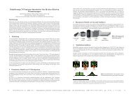
cause a variety of damage [5][39]. Figure 11 shows that even a<br />
low-volume void causes a failure if placed directly underneath the<br />
via, whereas a void <strong>in</strong> a via-below c<strong>on</strong>figurati<strong>on</strong> has to grow<br />
larger before the <strong>in</strong>terc<strong>on</strong>nect is destroyed.<br />
Via-above C<strong>on</strong>figurati<strong>on</strong><br />
Metal1 Cu<br />
Via-below C<strong>on</strong>figurati<strong>on</strong><br />
Metal1 Cu e -<br />
e -<br />
Void<br />
Metal2 Cu<br />
Void<br />
Metal2 Cu<br />
Ta/TaN<br />
L<strong>in</strong>er Layer<br />
SiN, NSiC<br />
Cap Layer<br />
Low <br />
Dielectric<br />
Ta/TaN<br />
L<strong>in</strong>er Layer<br />
SiN, NSiC<br />
Cap Layer<br />
Low <br />
Dielectric<br />
Figure 11. Via-above <str<strong>on</strong>g>and</str<strong>on</strong>g> via-below c<strong>on</strong>figurati<strong>on</strong>s with their<br />
different damage locati<strong>on</strong>s partly due to the <strong>in</strong>terface/surface<br />
diffusi<strong>on</strong> prevalent <strong>in</strong> copper wires.<br />
5.6 Surface Coat<strong>in</strong>g / Metal Capp<strong>in</strong>g<br />
As menti<strong>on</strong>ed <strong>in</strong> Secti<strong>on</strong> 2, the Cu/cap layer <strong>in</strong>terface is the<br />
dom<strong>in</strong>ant diffusi<strong>on</strong> path for electromigrati<strong>on</strong> <strong>in</strong> submicr<strong>on</strong> copper<br />
<strong>in</strong>terc<strong>on</strong>nects. <str<strong>on</strong>g>Electromigrati<strong>on</strong></str<strong>on</strong>g> studies <strong>in</strong> copper l<strong>in</strong>e structures<br />
show that mass transport is dom<strong>in</strong>ated by diffusi<strong>on</strong> at the Cu/cap<br />
layer <strong>in</strong>terface, probably due to the presence of defects (voids)<br />
<strong>in</strong>duced by the chemical mechanical polish (CMP) process prior<br />
to cap depositi<strong>on</strong> [11][35]. The effect of a dielectric capp<strong>in</strong>g layer<br />
<strong>on</strong> <strong>in</strong>terfacial mass transport for copper <strong>in</strong>terc<strong>on</strong>nects can<br />
therefore be exploited. For that purpose cap layers which <strong>in</strong>crease<br />
activati<strong>on</strong> energies at the <strong>in</strong>terface <str<strong>on</strong>g>and</str<strong>on</strong>g> which provide a high<br />
degree of stiffness (see Secti<strong>on</strong> 5.2) will improve EM resistance.<br />
For example, Hu et al. [16] dem<strong>on</strong>strated a significant<br />
improvement <strong>in</strong> EM lifetime by coat<strong>in</strong>g the Cu surface with a th<strong>in</strong><br />
10-nm electroless layer of CoWP.<br />
5.7 Frequency Dependency<br />
The lifetime of a wire carry<strong>in</strong>g alternat<strong>in</strong>g currents (AC) is<br />
significantly l<strong>on</strong>ger than that of a wire with direct currents (DC),<br />
due to damage-heal<strong>in</strong>g effects (Figure 12). Material migrat<strong>in</strong>g <strong>in</strong><br />
<strong>on</strong>e directi<strong>on</strong> can partially migrate back to its orig<strong>in</strong>al locati<strong>on</strong><br />
under beneficial c<strong>on</strong>diti<strong>on</strong>s. C<strong>on</strong>sequently, the <strong>in</strong>terc<strong>on</strong>nect<br />
suffers less damage from electromigrati<strong>on</strong> under AC c<strong>on</strong>diti<strong>on</strong>s.<br />
Experiments <strong>in</strong> [38] reveal that the effect of self-heal<strong>in</strong>g becomes<br />
noticeable above 10 Hz <str<strong>on</strong>g>and</str<strong>on</strong>g> <strong>in</strong>creases with the switch<strong>in</strong>g<br />
frequency up to about 10 kHz where it reaches a saturati<strong>on</strong> value.<br />
There is no improvement <strong>in</strong> circuit durability at frequencies above<br />
this po<strong>in</strong>t.<br />
Tao et al. [38] report that AC lifetime at high frequencies is<br />
typically over 1,000 times l<strong>on</strong>ger for Al-2% Si <str<strong>on</strong>g>and</str<strong>on</strong>g> Al-4% Cu <str<strong>on</strong>g>and</str<strong>on</strong>g><br />
over 500 times l<strong>on</strong>ger for Cu <strong>in</strong>terc<strong>on</strong>nects.<br />
As a c<strong>on</strong>sequence, two different sets of maximum allowable<br />
current densities are comm<strong>on</strong>ly used <strong>in</strong> practical current-density<br />
verificati<strong>on</strong>, <strong>on</strong>e for signal nets with frequencies above 10 kHz<br />
<str<strong>on</strong>g>and</str<strong>on</strong>g> <strong>on</strong>e for the rema<strong>in</strong><strong>in</strong>g (DC) nets, such as power supply l<strong>in</strong>es.<br />
MTTF (AC)<br />
MTTF (DC)<br />
10 3<br />
10 2<br />
10 1<br />
10 0<br />
10 -2<br />
10 -1<br />
10 0<br />
10 1<br />
10 2<br />
10 3<br />
Frequency <strong>in</strong> Hz<br />
10 4<br />
Figure 12. Mean time to failure (MTTF) if <strong>in</strong>terc<strong>on</strong>nect is<br />
stressed by an alternat<strong>in</strong>g current (AC) compared to MTTF if a<br />
directed current (DC) is applied [38].<br />
6. OUTLOOK<br />
<str<strong>on</strong>g>Electromigrati<strong>on</strong></str<strong>on</strong>g> (EM) is becom<strong>in</strong>g an <strong>in</strong>creas<strong>in</strong>gly difficult<br />
design challenge due to higher <strong>in</strong>terc<strong>on</strong>nect current densities. The<br />
<strong>on</strong>-go<strong>in</strong>g trend <strong>in</strong> IC downscal<strong>in</strong>g is produc<strong>in</strong>g physical designs<br />
with ever-smaller feature sizes, which can easily give rise to<br />
current densities that exceed their maximum allowable value.<br />
In order to address this problem dur<strong>in</strong>g layout synthesis, this talk<br />
has focused <strong>on</strong> basic design issues that affect electromigrati<strong>on</strong><br />
dur<strong>in</strong>g <strong>in</strong>terc<strong>on</strong>nect physical design. The aim is to <strong>in</strong>crease<br />
current density limits <strong>in</strong> the <strong>in</strong>terc<strong>on</strong>nect by utiliz<strong>in</strong>g<br />
electromigrati<strong>on</strong>-<strong>in</strong>hibit<strong>in</strong>g measures, such as short-length <str<strong>on</strong>g>and</str<strong>on</strong>g><br />
reservoir effects. Exploitati<strong>on</strong> of these effects at the layout stage<br />
provides partial relief of EM c<strong>on</strong>cerns <strong>in</strong> today’s design flows.<br />
In order to use these effects <strong>in</strong> next generati<strong>on</strong> design flows, we<br />
propose establish<strong>in</strong>g a dependence between the applied current<br />
density limits <strong>on</strong> the specific circuit geometry <str<strong>on</strong>g>and</str<strong>on</strong>g> the<br />
applicati<strong>on</strong>’s missi<strong>on</strong> profile. <strong>Design</strong> tools can significantly<br />
improve the EM robustness of the generated layout by utiliz<strong>in</strong>g<br />
EM-optimized layout c<strong>on</strong>figurati<strong>on</strong>s as c<strong>on</strong>stra<strong>in</strong>ts dur<strong>in</strong>g<br />
synthesis steps, such as rout<strong>in</strong>g. We believe that this <strong>in</strong>clusi<strong>on</strong> of<br />
EM-specific requirements <strong>in</strong> the physical design can provide<br />
relief from severe reliability c<strong>on</strong>stra<strong>in</strong>ts <strong>in</strong> future technologies.<br />
ACKNOWLEDGEMENTS<br />
The author wishes to thank Matthias Thiele <str<strong>on</strong>g>and</str<strong>on</strong>g> Tilo Meister for<br />
their c<strong>on</strong>tributi<strong>on</strong>s to this paper. This work was d<strong>on</strong>e <strong>in</strong> close<br />
collaborati<strong>on</strong> with Göran Jerke at Robert Bosch GmbH <str<strong>on</strong>g>and</str<strong>on</strong>g><br />
Shanthi Siemes <str<strong>on</strong>g>and</str<strong>on</strong>g> Uwe Hahn of GlobalFoundries Inc. Their<br />
valuable practical <strong>in</strong>put is greatly appreciated.<br />
REFERENCES<br />
[1] V. K. Andleigh, V. T. Srikar, Y.-J. Park, C. V. Thomps<strong>on</strong>, “Mechanism<br />
maps for electromigrati<strong>on</strong>-<strong>in</strong>duced failure of metal <str<strong>on</strong>g>and</str<strong>on</strong>g> alloy<br />
<strong>in</strong>terc<strong>on</strong>nects,” J. Appl. Phys. 86 (1999), 6737. DOI=<br />
http://dx.doi.org/10.1063/1.371750<br />
[2] L. Arnaud, G. Tartavel, T. Berger, D. Mariolle, Y. Gobil, I. Touet,<br />
“Microstructure <str<strong>on</strong>g>and</str<strong>on</strong>g> electromigrati<strong>on</strong> <strong>in</strong> copper damascene l<strong>in</strong>es,” Proc.<br />
37th Annual Reliability Physics Symposium (1999), 263 -269. DOI=<br />
http://dx.doi.org/10.1109/RELPHY.1999.761624<br />
[3] J. R. Black, “<str<strong>on</strong>g>Electromigrati<strong>on</strong></str<strong>on</strong>g> – A brief survey <str<strong>on</strong>g>and</str<strong>on</strong>g> some recent<br />
results,” IEEE Trans. <strong>on</strong> Electr<strong>on</strong>ic Devices (April 1969), 338-347.<br />
DOI= http://dx.doi.org/10.1109/T-ED.1969.16754<br />
10 5<br />
10 6<br />
10 7<br />
10 8<br />
39