Why Silicon Photonics? - Institute of Microelectronics - A*Star
Why Silicon Photonics? - Institute of Microelectronics - A*Star
Why Silicon Photonics? - Institute of Microelectronics - A*Star

Create successful ePaper yourself
Turn your PDF publications into a flip-book with our unique Google optimized e-Paper software.
An ISO 9001 Certified Organisation<br />
A publication <strong>of</strong> the <strong>Institute</strong> <strong>of</strong> <strong>Microelectronics</strong><br />
Issue 3 October 2009<br />
B u l l e t i n<br />
EISSN 0218-7477 MICA (P) 193/04/2009<br />
<strong>Why</strong> <strong>Silicon</strong><br />
<strong>Photonics</strong>?<br />
Monolithic 10 Gbs -1<br />
<strong>Silicon</strong> Optical<br />
Modulators<br />
Diffraction<br />
Grating Effect<br />
on Waveguided<br />
Germanium MSM<br />
Photodetector<br />
Response<br />
Germanium<br />
Photodetector<br />
Technology for<br />
Next Generation<br />
Optical Interconnects<br />
Applications<br />
Light Extraction<br />
Improvement from<br />
Si-based Multilayers<br />
with Photonic<br />
Crystal Patterns<br />
Exclusive Interviews:<br />
Dr. Young-Kai Chen<br />
Bell Laboratories, Alcatel-Lucent<br />
Pr<strong>of</strong>essor Fujio Masuoka<br />
Unisantis Electronics (Japan) Ltd.
Executive Director’s<br />
Foreword<br />
Kwong Dim-Lee<br />
Executive Director<br />
Dear Readers,<br />
As we live through the Information Age, we witnessed the progression <strong>of</strong> smoke signals to Morse code,<br />
analog voice transmission to digital voice/video/data content and now massive bandwidth demand for<br />
data communication. The image communications with the World Wide Web created further bandwidth<br />
demand and the advent <strong>of</strong> interactive computation and imaging activities drive even higher bandwidth<br />
requirements. Optical interconnect technology has been utilized in long haul communications for the past<br />
two to three decades but its applications in short reach communication is not widespread primarily due<br />
to its cost. <strong>Silicon</strong> <strong>Photonics</strong> has emerged as a viable alternative for high volume manufacture <strong>of</strong> photonic<br />
integrated circuits.<br />
In analogy to what <strong>Silicon</strong> has done for <strong>Silicon</strong> Electronics and how it influenced our daily life and business<br />
operation, <strong>Silicon</strong> <strong>Photonics</strong> is set to revolutionize the traditional multi-billion-dollar optoelectronics<br />
industry. In the near future, applications that can benefit from <strong>Silicon</strong> <strong>Photonics</strong> include high data-rate<br />
communications (tera-bit, i.e., 10 12 bit) and high-performance computing. Possible applications <strong>of</strong> silicon<br />
photonics include optical communications, environmental monitoring, chemical and biochemical analysis, medical, healthcare and<br />
diagnostic areas.<br />
To promote Singapore’s competitive edge at the forefront <strong>of</strong> this emerging technology, the <strong>Institute</strong> <strong>of</strong> <strong>Microelectronics</strong> (IME) has<br />
made significant contributions to the establishment <strong>of</strong> a cost effective <strong>Silicon</strong> <strong>Photonics</strong> technology platform since late 2006. The<br />
central goal <strong>of</strong> the Nano-<strong>Photonics</strong> programme is focused on the development <strong>of</strong> process technologies and designs needed to<br />
develop application-specific electronic-photonic integrated circuit (AS-EPIC). By leveraging on the well established Si-CMOS<br />
fabrication technology, IME <strong>Photonics</strong> Team has successfully built up a comprehensive passive and active photonic device library<br />
with versatile building blocks required to support the design and demonstration <strong>of</strong> EPIC. In this issue <strong>of</strong> MicroE, we will be providing<br />
readers an overview <strong>of</strong> IME’s research and development in this technology.<br />
Editorial Team<br />
Kwong Dim-Lee<br />
Teo Yong Chua<br />
Tan Su-Lynn<br />
Contributors<br />
Kwong Dim-Lee<br />
Teo Yong Chua<br />
Tan Su-Lynn<br />
Patrick Lo G.Q.<br />
Ang Kah-Wee<br />
Liow Tsung-Yang<br />
Yu Mingbin<br />
Ren Fang-Fang<br />
Guest Interviewees<br />
Dr. Young-Kai Chen <strong>of</strong> Bell Laboratories,<br />
Alcatel-Lucent<br />
Pr<strong>of</strong>essor Fujio Masuoka <strong>of</strong> Unisantis<br />
Electronics (Japan) Ltd<br />
For enquiries and comments, please write to:<br />
IME Editorial Team<br />
<strong>Institute</strong> Of <strong>Microelectronics</strong><br />
11 Science Park Road<br />
Singapore Science Park II<br />
Singapore 117685<br />
Tel: +65 6779 7522<br />
Fax: +65 6778 0136<br />
Email: editorial@ime.a-star.edu.sg<br />
www.ime.a-star.edu.sg<br />
For research collaboration and business opportunities,<br />
please email: ID@ime.a-star.edu.sg<br />
microE Bulletin is a bi-yearly publication <strong>of</strong> IME.<br />
All Rights Reserved. No part <strong>of</strong> this publication may be reproduced or used<br />
in any form without the written permission <strong>of</strong> IME.<br />
THIS MONTH: OCTOBER 2009<br />
COVER STORY<br />
3 Germanium Photodetector Technology for Next<br />
Generation Optical Interconnects Applications<br />
R&D NEWS<br />
8 <strong>Why</strong> <strong>Silicon</strong> <strong>Photonics</strong><br />
10 Monolithic 10 Gbs -1 <strong>Silicon</strong> Optical Modulators<br />
11 Diffraction Grating Effect on Waveguided Germanium<br />
MSM Photodetector Response<br />
13 Light Extraction Improvement from<br />
Si-based Multilayers with Photonic Crystal Patterns<br />
INDUSTRY COLLABORATIONS<br />
Exclusive Interviews:<br />
16 Dr. Young-Kai Chen <strong>of</strong> Bell Laboratories,<br />
Alcatel-Lucent<br />
17 Pr<strong>of</strong>essor Fujio Masuoka <strong>of</strong> Unisantis Electronics<br />
(Japan) Ltd.<br />
PEOPLE<br />
18 Zhao Hui, a former PhD student attached to IME<br />
19 Jiang Yu, PhD graduate from NUS<br />
A Research <strong>Institute</strong> <strong>of</strong> the Agency for Science, Technology and Research (A*STAR)
Cover<br />
Story<br />
Germanium Photodetector Technology<br />
for Next Generation Optical Interconnects<br />
Applications<br />
Dr. Ang Kah-Wee<br />
Senior Research Engineer, Nano-<br />
Electronics and <strong>Photonics</strong> Programme<br />
Dr. Patrick Lo G. Q.<br />
Program Director, Nano-Electronics<br />
and <strong>Photonics</strong> Programme<br />
Executive Summary<br />
Research into the limits <strong>of</strong><br />
electrical interconnects indicates<br />
that the requirements for data<br />
communication in future generations <strong>of</strong><br />
CMOS integrated circuits can hardly be<br />
met with metal wires. While the demand<br />
for on-chip functionality continues to<br />
grow as predicted by Moore’s Law, it<br />
is now widely recognized that copper<br />
interconnect will increasingly suffer from<br />
severe propagation delays for clock<br />
signals, overheating, information latency<br />
and electromagnetic interference. Optical<br />
interconnects which readily <strong>of</strong>fer greater<br />
bandwidth, lower power, and resistance<br />
to electromagnetic interference and<br />
signal crosstalk has emerged as one<br />
promising alternative that has attracted<br />
growing interests. This article presents<br />
a brief perspective on the exploration<br />
<strong>of</strong> silicon photonics to provide high<br />
performance optical interconnects<br />
solutions to support the growing needs<br />
<strong>of</strong> data communication. In particular,<br />
the progress and development <strong>of</strong> optical<br />
detections technology using Group-IV<br />
based heterostructure materials are<br />
reviewed. A successful implementation<br />
<strong>of</strong> such state-<strong>of</strong>-the-art Ge-based<br />
photodetector technologies is poised to<br />
become an enabling technology to realize<br />
on-chip optical interconnects for nextgeneration<br />
high bandwidth computing<br />
applications. The overall goal is to<br />
develop a scalable approach that extends<br />
the reach and impact <strong>of</strong> Moore’s Law for<br />
many more generations to come.<br />
Introduction<br />
Continuous scaling <strong>of</strong> complementary<br />
metal-oxide-semiconductor (CMOS)<br />
transistor technology as driven by<br />
Moore’s Law leads to significant<br />
enhancement in the speed performance<br />
<strong>of</strong> microprocessor. Over the past<br />
few decades, this was achieved by<br />
aggressively shrinking the physical<br />
dimension <strong>of</strong> the transistor from one<br />
technology generation to another for<br />
improved drivability and integrated circuits<br />
density. Recent advancement in CMOS<br />
extension via innovative ‘More Moore’<br />
approaches such as the application <strong>of</strong><br />
strained channel engineering, metal gate/<br />
high- , and multiple gate structure have<br />
pushed the device performance closer to<br />
its fundamental limits. This has led to a<br />
new generation <strong>of</strong> microprocessors that<br />
are capable <strong>of</strong> handling data computation<br />
at a rate that outpaces their abilities<br />
to transmit or receive it from external<br />
circuits.<br />
However, the evolution <strong>of</strong> Moore’s Law<br />
will soon encounter red-brick walls.<br />
Though the CMOS transistors switching<br />
speed has been significantly enhanced,<br />
the performance gain at the system<br />
level does not seem to match up with<br />
the improvement. This is because a<br />
higher transistor packing density leads<br />
to an increased demand for longer<br />
interconnects, which resulted in a<br />
higher parasitic resistance. Moreover,<br />
the additional capacitive coupling also<br />
causes longer signal delay and power<br />
consumption. While there is a tendency<br />
in high performance computing system to<br />
shifts towards increasing the parallelism<br />
in data processing by partitioning the<br />
microprocessor into multi-cores, such<br />
approach is perceived to be unable to<br />
<strong>of</strong>fer the ultimate solution. The complexity<br />
introduced in this approach is enormous,<br />
and will eventually strained in meeting the<br />
requirements <strong>of</strong> low power consumption<br />
and high bandwidth data communication<br />
beyond 10Gb/s. Thus, there is an<br />
obvious need to create a radically new<br />
communication technology landscape<br />
to meet the stringent requirements <strong>of</strong><br />
data communication in future technology<br />
generations.<br />
Optical interconnect technology is an<br />
increasingly attractive alternative and<br />
has become essential for computing<br />
and communication industries. This<br />
is because optical interconnects <strong>of</strong>fer<br />
advantages such as greater bandwidth,<br />
lower power, reduced interconnects<br />
delay, and immunity to electro-magnetic<br />
interference and signal crosstalk. Over<br />
the last few decades, traditional optical<br />
components are typically made <strong>of</strong><br />
exotic III-V compound materials such<br />
as gallium-arsenide (GaAs) and indiumphosphide<br />
(InP) due to their excellent<br />
light emission and absorption properties.<br />
However, compound-semiconductor<br />
devices are generally too complicated<br />
to process and costly to implement<br />
in optical interconnects. To be widely<br />
adopted, this technology must be made<br />
cost effective over the traditional copper<br />
interconnects approach. In search<br />
for such cost-competitive solution,<br />
Si photonics emerges to hold great<br />
promise for its inexpensive material and<br />
its compatibility with current CMOS<br />
fabrication technology. In addition, the<br />
ability to integrate different types <strong>of</strong> optical<br />
components such as photodetector,<br />
modulator, light source, and waveguide<br />
to form a photonics integrated circuit on<br />
a single silicon chip platform makes it an<br />
extremely favourable approach.<br />
Figure 1 shows a schematic illustration<br />
<strong>of</strong> the essential optical components<br />
to construct a photonics integrated<br />
circuit for data communication. In a way<br />
analogous to powering the electronic<br />
www.ime.a-star.edu.sg<br />
microE Bulletin | Issue 3 October 2009 3
Cover<br />
Story<br />
regime (1.3~1.55μm), germanium (Ge)<br />
could be exploited as alternative for<br />
the realization <strong>of</strong> high performance<br />
photodetector due to its favourable<br />
absorption coefficient. However, Ge can<br />
be a challenging material to integrate in<br />
a CMOS environment for its low thermal<br />
budget constraint and its large lattice<br />
mismatch <strong>of</strong> ~4.2% with Si [1]. High defect<br />
densities seen in the Ge-on-<strong>Silicon</strong>on-<br />
Insulator (Ge-on-SOI) epitaxial film could<br />
induce unfavourable carrier recombination<br />
process that would degrade the detector’s<br />
quantum efficiency.<br />
Development <strong>of</strong> Hetero-Epitaxy <strong>of</strong><br />
Germanium on <strong>Silicon</strong><br />
Figure 1: Schematic illustration <strong>of</strong> on-chip optical interconnects realized using a photonics integrated<br />
circuit platform.<br />
circuit using an electrical power supply,<br />
a high quantum efficiency laser source<br />
is employed to provide the required<br />
optical power in a photonics integrated<br />
circuit. By leveraging on the high index<br />
contrast between the Si core and the<br />
silicon-dioxide cladding, routing <strong>of</strong><br />
optical signals using photonic waveguide<br />
with low propagation loss can be<br />
made possible. To harness increased<br />
data capacity, a wavelength division<br />
multiplexing (WDM) based on arrayedwaveguide<br />
grating (AWG) composed<br />
<strong>of</strong> rib SOI waveguides or ring resonator<br />
in photonic domain can be exploited to<br />
provide multiple channels transmission<br />
for parallel data processing. Using an<br />
optical filter, a particular wavelength<br />
(λ n<br />
) can be selected into the photonic<br />
waveguide data bus. While Si-based<br />
modulator exhibits weaker electrooptical<br />
coefficients due to its central symmetry in<br />
the lattice structure, a free carrier plasma<br />
dispersion effect can be exploited to<br />
enable effective optical modulation. The<br />
modulated optical signals are channelled<br />
through the photonic waveguide data bus<br />
where multiple wavelengths signals can<br />
be delivered on the same channel without<br />
suffering interference from one another.<br />
At the receiving end, signal <strong>of</strong> a specific<br />
wavelength channel is filtered and fed<br />
into a photodetector for enabling opticalto-electrical<br />
encoding. The encoded<br />
electrical signal will then pass through the<br />
CMOS circuitry for data processing.<br />
Although it appears promising that an<br />
electronic-photonic integration could<br />
enable the convergence <strong>of</strong> computing<br />
and communication capabilities on<br />
single ship platform, its wide spread<br />
implementation has been hindered by<br />
the grand challenge in demonstrating an<br />
important active photonic component<br />
needed to perform opto-electric (OE)<br />
signal conversion. The search for a new<br />
material that is compatible with the<br />
mainstream CMOS process technology is<br />
<strong>of</strong> particular interest. While silicon (Si) has<br />
been shown to be unsuitable for optical<br />
detection in the near-infrared wavelength<br />
The key challenge to high quality<br />
germanium (Ge) epitaxy growth on silicon<br />
(Si) rests with the huge lattice mismatch<br />
between the two heterostructure<br />
materials. The existence <strong>of</strong> ~4.2% lattice<br />
mismatch strain has been shown to<br />
give rise to two major issues: (1) high<br />
densities <strong>of</strong> threading dislocations and<br />
(2) rough surface morphology due to 3D<br />
Stranski-Krastanov (SK) growth. Both <strong>of</strong><br />
these defects present much concerns<br />
for the generation <strong>of</strong> high leakage<br />
current which would compromise the<br />
efficiency <strong>of</strong> a photodetector. Strategies<br />
proposed in the literature to overcome<br />
these challenges vary to a large extent.<br />
Colace et al. proposed a direct heteroepitaxy<br />
growth <strong>of</strong> Ge on Si through the<br />
use <strong>of</strong> a low temperature thin SiGe buffer<br />
layer (a few 10nm) [2]. The insertion <strong>of</strong><br />
such thin buffer avoids the occurrence<br />
<strong>of</strong> 3D SK growth and allows the misfit<br />
dislocations to be concentrated at<br />
the hetero-interfaces. However such<br />
approach requires a cyclic annealing<br />
process to be carried out at both high<br />
and low temperature (900°C/780°C) to<br />
reduce the threading dislocation density<br />
within the Ge active film. Using a similar<br />
cyclic thermal annealing approach, Luan<br />
et al. had also demonstrated a significant<br />
improvement in both the surface<br />
roughness and the dislocation density<br />
[1]. Unfortunately, the needs for a high<br />
temperature post-epitaxy Ge anneal with<br />
long cycle time present a major concern<br />
for CMOS implementation.<br />
4 <strong>Institute</strong> <strong>of</strong> <strong>Microelectronics</strong>
Cover<br />
Story<br />
In our approach, selective epitaxial<br />
growth <strong>of</strong> Ge on silicon-on-insulator<br />
(SOI) was performed using an ultra-high<br />
vacuum chemical vapor deposition<br />
reactor [3]-[13]. Unlike the conventional<br />
approaches, a thin pseudo-graded<br />
SiGe buffer with a thickness <strong>of</strong> ~20nm<br />
is proposed in this study to relieve the<br />
large lattice mismatch stress between<br />
the two heterostructure materials (Figure<br />
2). The Ge mole fraction within the SiGe<br />
buffer is compositionally graded from<br />
10% to ~50%. The precursor gases used<br />
for the SiGe growth comprise <strong>of</strong> diluted<br />
germane (GeH 4<br />
) and pure disilane (Si 2<br />
H 6<br />
).<br />
A relatively thin Ge seed layer <strong>of</strong> ~30nm<br />
is subsequently grown on the SiGe buffer<br />
at a process temperature <strong>of</strong> 370°C.<br />
The use <strong>of</strong> a low temperature growth is<br />
intended to suppress adatoms migration<br />
on Si and thus prevents the formation<br />
<strong>of</strong> 3D SK growth, which allows a flat<br />
Ge surface morphology to be achieved.<br />
Upon obtaining a smooth Ge seed layer,<br />
the epitaxy process temperature is then<br />
increased to ~550°C to facilitate faster<br />
epitaxy growth to obtain the desired Ge<br />
thickness. Using this approach, high<br />
quality Ge epilayer with a thickness <strong>of</strong><br />
up to ~2μm has been demonstrated,<br />
along with the achievement <strong>of</strong> threading<br />
dislocation density as low as ~107 cm -2<br />
without undergoing any high temperature<br />
cyclical thermal annealing step. In<br />
addition, selective area growth <strong>of</strong> Ge on Si<br />
has also been developed using a cyclical<br />
deposition and etch back approach. In<br />
each deposition cycle, the Ge growth<br />
time is carefully optimized to avoid<br />
exceeding the incubation time needed<br />
for Ge seeds to nucleate on the dielectric<br />
film. After every Ge deposition cycle, a<br />
short etch back process using chlorine<br />
(Cl 2<br />
) precursor gas is then introduced<br />
to remove possible Ge nucleation sites<br />
on the dielectric. This allows a highly<br />
selective Ge epitaxy process to be<br />
developed, along with the achievement <strong>of</strong><br />
excellent surface roughness <strong>of</strong> ~0.28nm.<br />
Waveguided Ge Photodetector<br />
Platform Technology<br />
For future realization <strong>of</strong> ultra-compact<br />
photonics integrated circuit, the<br />
integration <strong>of</strong> Ge photodetector with<br />
optical waveguide and the demonstration<br />
<strong>of</strong> high sensitivity with thin Ge epilayer<br />
(
Cover<br />
Story<br />
the optical mode within the core <strong>of</strong> the Si<br />
waveguide so as to prevent leakage into<br />
the underneath Si substrate.<br />
Performance Metrics <strong>of</strong> Waveguided<br />
Ge Photodetector<br />
Figure 4(a) examines the current-voltage<br />
characteristics <strong>of</strong> the VPD and LPD<br />
detectors under dark and illumination<br />
conditions. Excellent rectifying<br />
characteristics were demonstrated in<br />
both the detectors, showing a forwardto-reverse<br />
current ratio <strong>of</strong> ~4 orders <strong>of</strong><br />
magnitude. For a given applied bias <strong>of</strong><br />
−1.0V, the dark current (I dark<br />
) in a VPD<br />
was measured to be ~0.57μA (or ~0.7nA/<br />
μm 2 ), which is below the typical 1.0μA<br />
generally considered to be the upper limit<br />
for high speed receiver design. On the<br />
other hand, the dark current performance<br />
in a LPD showed a much higher I dark<br />
value<br />
<strong>of</strong> ~3.8μA (or ~1.9nA/μm 2 ).<br />
the VPD and LPD detectors achieved a<br />
comparable photocurrent level at high<br />
applied biases beyond -1.0V. Figure<br />
4(b) compares the responsivity <strong>of</strong> the<br />
detectors as a function <strong>of</strong> the applied<br />
voltages. It is interesting to note that<br />
the vertical PIN detector demonstrated<br />
a lower responsivity as compared to the<br />
lateral PIN detector for biases below−0.5<br />
V. This could possibly be due to an<br />
enhanced carrier recombination process<br />
at the high density <strong>of</strong> defect centres near<br />
the Ge-Si heterojunction. This is set to<br />
compromise the absolute photocurrent<br />
value <strong>of</strong> a vertical PIN detector under low<br />
field influence. For an applied bias larger<br />
than −1.0 V, a comparable responsivity<br />
was measured for both the vertical and<br />
lateral PIN detectors. Despite that the<br />
metallurgical junction is separated by<br />
merely 0.8μm, a lateral PIN detector also<br />
showed a high absolute responsivity <strong>of</strong><br />
~0.9 A/W.<br />
compared to that <strong>of</strong> LPD detector with<br />
a slightly larger FWHM <strong>of</strong> ~28.9ps.<br />
This could be attributed to the smaller<br />
depletion layer width design in a VPD<br />
detector which reduces the carrier transit<br />
time. The FWHM pulse width is related<br />
to the bandwidth and can be used as a<br />
metric to gauge the speed performance <strong>of</strong><br />
the detectors. The theoretical modelling<br />
results <strong>of</strong> the RC-time constant and the<br />
transit-time bandwidth are also plotted<br />
in Figure 5(b). Reducing the depletion<br />
spacing could be exploited to enhance<br />
the transit-time bandwidth performance<br />
significantly, but it could impose concern<br />
for a degraded RC-time bandwidth. To<br />
overcome such trade-<strong>of</strong>f, one could scale<br />
the detector’s optical absorption length<br />
to achieve lower device capacitance for<br />
enabling bandwidth improvement.<br />
Industry Collaborations and MPW<br />
Services<br />
In order to compare the sensitivity<br />
performance between the VPD and LPD,<br />
optical measurements were performed<br />
by injecting an incident photon with<br />
a wavelength <strong>of</strong> 1550nm into the SOI<br />
micro-waveguide. The typical optical<br />
propagation loss in our SOI microwaveguide<br />
under TE polarization mode<br />
is ~2dB/cm. No coupler was integrated<br />
with the Si waveguide and the incidence<br />
light was coupled through a single mode<br />
lensed fiber directly into the Si nano-taper.<br />
For an incident light power <strong>of</strong> ~300μW,<br />
optical measurements showed that both<br />
To investigate the factors affecting the<br />
speed performance <strong>of</strong> the VPD and LPD<br />
detectors used in this study, impulse<br />
response measurements were performed<br />
at a photon wavelength <strong>of</strong> 1550nm. A<br />
pulsed laser source having a 80fs pulse<br />
width was used in the measurements.<br />
Both the detectors were characterized<br />
using microwave probes and the impulse<br />
responses were captured with a high<br />
speed sampling oscilloscope. Figure<br />
5(a) shows that a VPD detector achieved<br />
a smaller full-width-at-half-maximum<br />
(FWHM) pulse width <strong>of</strong> ~24.4ps as<br />
Figure 4: (a) The current-voltage characteristics <strong>of</strong> the VPD and LPD detectors measured under dark<br />
and illumination conditions. (b) Responsivity as a function <strong>of</strong> applied voltages for both the VPD and LPD<br />
detectors measured at a wavelength <strong>of</strong> 1550nm.<br />
Since the inception <strong>of</strong> silicon photonics<br />
program in 2006, the <strong>Institute</strong> <strong>of</strong><br />
<strong>Microelectronics</strong> (IME) has been<br />
actively engaged with industry partners<br />
in developing and prototyping high<br />
performance optical components and<br />
photonics integrated circuits. Such<br />
prototyping services can be divided into<br />
two categories - Multi-Project-Wafer<br />
(MPW) prototyping and customized<br />
prototyping, both <strong>of</strong> which <strong>of</strong>fer high-end<br />
fabrication services at a cost affordable<br />
to research groups and companies.<br />
MPW prototyping works on the principle<br />
<strong>of</strong> combining designs from various<br />
users on shared masks, sharing a large<br />
fraction <strong>of</strong> the process cost among the<br />
users. On the other hand, many <strong>of</strong> IME’s<br />
existing partners welcome the flexibility<br />
that customized prototyping <strong>of</strong>fers. To<br />
shorten the development life-cycle, IME<br />
also provides a host <strong>of</strong> both active and<br />
passive baseline photonic devices in its<br />
design libraries. Fabrication is performed<br />
using standard CMOS processes in its<br />
200 mm R&D foundry, which facilitates<br />
quick technology transfers to commercial<br />
foundries for mass production. The<br />
service has proven to be a boost for users<br />
- fabless companies and research groups.<br />
An excellent example <strong>of</strong> a company<br />
which has benefited from this service<br />
6 <strong>Institute</strong> <strong>of</strong> <strong>Microelectronics</strong>
Cover<br />
Story<br />
Figure 5: (a) Impulse responses <strong>of</strong> the VPD and LPD detectors measured at a wavelength <strong>of</strong> 1550nm.<br />
A smaller FWHM pulse width <strong>of</strong> ~24.4 ps was achieved in a VPD as compared to a LPD with a pulse<br />
width <strong>of</strong> ~28.9ps. (b) Downscaling <strong>of</strong> detector length results in bandwidth enhancement due to a<br />
reduced device capacitance.<br />
is Lightwire, a US-based interconnect<br />
company.<br />
The Future Evolution <strong>of</strong> <strong>Silicon</strong><br />
<strong>Photonics</strong><br />
The future evolution <strong>of</strong> <strong>Silicon</strong> <strong>Photonics</strong><br />
will become increasingly promising<br />
with the development <strong>of</strong> cutting edge<br />
nanophotonic technologies. As the<br />
electronics devices continue to scale in<br />
advanced CMOS technology nodes, the<br />
foot-print <strong>of</strong> existing photonics devices<br />
which are typically in the micrometer<br />
scale seems to impose much constraint<br />
to enable the realization <strong>of</strong> ultra-compact<br />
electronic-photonic integrated circuit<br />
(EPIC). In order to address the needs<br />
for small form factor, low power and<br />
high speed integration while achieving<br />
costeffectiveness, the introduction <strong>of</strong><br />
Si nano-photonics solutions become<br />
imperative. However, aggressive<br />
downsizing <strong>of</strong> physical dimensions could<br />
compromise the device performance.<br />
Innovative approaches to enhance the<br />
efficiency <strong>of</strong> these nano-scale photonics<br />
devices are therefore highly desirable.<br />
For instance, the application <strong>of</strong> surface<br />
plasmon antenna technology to boost<br />
the quantum efficiency <strong>of</strong> nano-photodetector<br />
emerges as a practical solution.<br />
The discovery <strong>of</strong> surface plasmons can<br />
be exploited to generate resonance at the<br />
metal-dielectric interface with the same<br />
frequency as the impinging electromagnetic<br />
waves, but with a much shorter<br />
wavelength. By exploiting this effect,<br />
it becomes possible to guide optical<br />
signals in nanoscale structures, resulting<br />
in the miniaturization <strong>of</strong> the photonic<br />
circuits. It is believed that nanophotonic<br />
technologies can potentially change the<br />
landscape for <strong>Silicon</strong> <strong>Photonics</strong>, allowing<br />
for greater miniaturization and taking the<br />
performance to new heights.<br />
References<br />
[1]<br />
[2]<br />
[3]<br />
[4]<br />
[5]<br />
[6]<br />
[7]<br />
H.-C. Luan, D. R. Lim, K. K. Lee, K. M. Chen, J. G. Sandland, K.<br />
Wada, and L. C. Kimerling, “High-quality Ge epilayers on Si with low<br />
threading-dislocation densities”, Applied Physics Letters, Vol. 75, No.<br />
19, pp. 2909–2911, 1999.<br />
L. Colace, G. Masini, and G. Assanto, “Ge-on-Si approaches to the<br />
detection <strong>of</strong> nearinfrared light”, IEEE Journal <strong>of</strong> Quantum Electronics,<br />
Vol. 35, No. 12, pp. 1843–1852, 1999.<br />
K.-W. Ang, T.-Y. Liow, M.-B. Yu, Q. Fang, J. Song, G.-Q. Lo, and D.-L<br />
Kwong, “Low thermal budget monolithic integration <strong>of</strong> evanescent<br />
coupled Ge-on-SOI photodetector on Si-CMOS platform”, IEEE<br />
Journal <strong>of</strong> Selected Topics in Quantum Electronics, Vol. 14, In Press.<br />
T.-Y. Liow, K.-W. Ang, Q. Fang, J. Song, Y. Xiong, M.-B. Yu, G.-Q. Lo,<br />
and D.-L. Kwong, “<strong>Silicon</strong> Modulators and Germanium Photodetectors<br />
on SOI: Monolithic Integration, Compatibility and Performance<br />
Optimization”, IEEE Journal <strong>of</strong> Selected Topics in Quantum<br />
Electronics, Vol. 14, In Press.<br />
K.-W. Ang, T.-Y. Liow, Q. Fang, M. B. Yu, F. F. Ren, S. Y. Zhu, J.<br />
Zhang, J. W. Ng, J. F. Song, Y. Z. Xiong, G. Q. Lo, and D.-L. Kwong,<br />
“<strong>Silicon</strong> <strong>Photonics</strong> Technologies for Monolithic Electronic-Photonic<br />
Integrated Circuit (EPIC) Applications: Current Progress and Future<br />
Outlook”, IEEE International Electron Device Meeting 2009, Baltimore,<br />
Dec. 7-9, 2009.<br />
K.-W. Ang, J. W. Ng, G.-Q. Lo, and D.-L. Kwong, “Impact <strong>of</strong> fieldenhanced<br />
band-trapsband tunneling on the dark current generation<br />
in germanium (Ge) p-i-n photodetector”, Applied Physics Letters, vol.<br />
94(22), 223515, Jun. 2009.<br />
J. Wang, W. Y. Loh, K. T. Chua, H. Zang, Y. Z. Xiong, S. M. F.<br />
Tan, M. B. Yu, S. J. Lee, G. Q. Lo, and D. L. Kwong, “Low-Voltage<br />
High-Speed (18 GHz/1 V) Evanescent-Coupled Thin-Film-Ge Lateral<br />
PIN Photodetectors Integrated on Si Waveguide”, IEEE <strong>Photonics</strong><br />
Technology Letters, vol. 20(17-20), pp. 1485–1487, Sep. 2008.<br />
[8]<br />
[9]<br />
K.-W. Ang, S. Y. Zhu, J. Wang, K. T. Chua, M. B. Yu, G. Q. Lo,<br />
and D. L. Kwong, “Novel <strong>Silicon</strong>-Carbon (Si:C) Schottky Barrier<br />
Enhancement Layer for Dark Current Suppression in Ge-on-SOI<br />
MSM Photodetectors”, IEEE Electron Device Letters, vol. 29(7), pp.<br />
708–710, Jul. 2008.<br />
K.-W. Ang, M.-B. Yu, S.-Y. Zhu, K.-T. Chua, G.-Q. Lo, and D.-L.<br />
Kwong, “Novel NiGe MSM Photodetector Featuring Asymmetrical<br />
Schottky Barriers using Sulfur Co-Implantation and Segregation”, IEEE<br />
Electron Device Letters, vol. 29(7), pp. 704–707, Jul. 2008.<br />
[10] K.-W. Ang, S. Zhu, M. Yu, G.-Q. Lo, and D.-L. Kwong, “High<br />
Performance Waveguided Ge-on-SOI Metal-Semiconductor-Metal<br />
Photodetectors with Novel <strong>Silicon</strong>-Carbon (Si:C) Schottky Barrier<br />
Enhancement Layer”, IEEE <strong>Photonics</strong> Technology Letters,vol. 20(9),<br />
pp. 754–756, May 2008. Germanium Photodetector Technologies for<br />
Next Generation Optical Interconnects Applications 9<br />
[11] S. Y. Zhu, M. B. Yu, G. Q. Lo, and D.-L. Kwong, “Near-infrared<br />
waveguide-based nickel silicide Schottky-barrier photodetector for<br />
optical communications”, Applied Physics Letters, Vol. 92, No. 8, p.<br />
081103, Feb. 2008.<br />
[12] W. Y. Loh, J. Wang, J. D. Ye, R. Yang, H. S. Nguyen, K. T. Chua, J.<br />
F. Song, T. H. Loh, Y. Z. Xiong, S. J. Lee, M. B. Yu, G. Q. Lo, and D.<br />
L. Kwong, “Impact <strong>of</strong> local strain from selective epitaxial germanium<br />
with thin Si/SiGe buffer on high-performance p-i-n photodetectors with<br />
a low thermal budget”, IEEE Electron Device Letters, vol. 28(11), pp.<br />
984–986, Nov. 2007.<br />
[13] T. H. Loh, H. S. Nguyen, R. Murthy, M. B. Yu, W. Y. Loh, G. Q. Lo, N.<br />
Balasubramanian, D. L. Kwong, J. Wang, and S. J. Lee, “Selective<br />
epitaxial germanium on silicon-on-insulator high speed photodetectors<br />
using low-temperature ultrathin Si 0.8<br />
Ge 0.2<br />
buffer”, Applied Physics<br />
Letters, Vol. 91, No. 7, p. 073503, Aug. 2007.<br />
www.ime.a-star.edu.sg<br />
microE Bulletin | Issue 3 October 2009 7
R&D News<br />
<strong>Why</strong> <strong>Silicon</strong> <strong>Photonics</strong>?<br />
Dr. Liow Tsung-Yang<br />
Senior Research Engineer, Nano-<br />
Electronics and <strong>Photonics</strong> Programme<br />
Dr. Patrick Lo G. Q.<br />
Program Director, Nano-Electronics<br />
and <strong>Photonics</strong> Programme<br />
The convergence <strong>of</strong> electronic and<br />
photonic technologies holds great<br />
promise for keeping up with the<br />
performance roadmap known as Moore’s<br />
Law. Today, it is generally known that high<br />
data rate communication beyond 10 Gb/s<br />
requires the replacement <strong>of</strong> conventional<br />
copper interconnect technology with<br />
optical interconnect technology, due<br />
to its advantages in bandwidth, power<br />
consumption and reach. Optical<br />
interconnect technology has been utilized<br />
in long haul communications for the<br />
past two to three decades. However, its<br />
presence in shorter reach applications is<br />
not widespread and has primarily been<br />
limited by cost. Due to rising bandwidth<br />
demands for short reach applications,<br />
there is potentially a huge market for<br />
optical technology. These include<br />
consumer applications such as Fiber-tothe-home<br />
(FTTH), which will enable the<br />
delivery <strong>of</strong> high bandwidth content such<br />
as high definition video and interactive<br />
entertainment to individual homes. There<br />
are also a variety <strong>of</strong> applications for<br />
much shorter reach optical interconnect<br />
technologies in the next-generation high<br />
performance computers.<br />
<strong>Silicon</strong> photonics is expected to play a<br />
vital role in the market growth <strong>of</strong> short<br />
to mid-range communications, since<br />
it combines both low-cost and massproductivity.<br />
<strong>Silicon</strong> is a compelling<br />
platform for integrated optics, with<br />
largely available infrastructure, toolsets,<br />
knowledge, and capacity that have been<br />
developed for <strong>Silicon</strong>-microelectronics.<br />
With the adoption <strong>of</strong> <strong>Silicon</strong> MEMS<br />
technique to create <strong>Silicon</strong>-trenches,<br />
grooves and other micro-structures, the<br />
cost <strong>of</strong> laser and fiber precision assembly<br />
can be significantly reduced. Perhaps the<br />
greatest benefit <strong>of</strong> <strong>Silicon</strong> photonics is<br />
the cost effectiveness, in addition to the<br />
performance gain via integrating different<br />
types <strong>of</strong> optical devices (e.g., signal<br />
routers, modulators, photodetectors) onto<br />
a single silicon platform together with the<br />
existing integrated electronics. Besides<br />
lowering production costs, <strong>Silicon</strong><br />
photonics also provides the facilities for<br />
product designers to add more integrated<br />
functions.<br />
On top <strong>of</strong> optical communications, <strong>Silicon</strong><br />
photonics may also be applied to new<br />
applications in environmental monitoring,<br />
chemical and biochemical analysis,<br />
medical, healthcare and diagnostic areas.<br />
All <strong>of</strong> these again have the common<br />
requirement <strong>of</strong> low cost, small form factor,<br />
and high-volume manufacturability, which<br />
will only be possible if one can deliver<br />
these technologies on an integrated<br />
silicon platform cost-effectively. In brief,<br />
the emerging demand for low-cost<br />
high-volume production <strong>of</strong> components<br />
with integrated functionality is the<br />
pull factor for <strong>Silicon</strong> photonics. Upon<br />
successful introduction <strong>of</strong> this technology,<br />
the impact it has on applications and the<br />
quality <strong>of</strong> human life will be <strong>of</strong> the same<br />
magnitude as what we have experienced<br />
from the introduction <strong>of</strong> electronic IC.<br />
IME’s <strong>Silicon</strong> <strong>Photonics</strong> Program<br />
IME’s <strong>Silicon</strong> <strong>Photonics</strong> Program was<br />
launched in late 2006. Since then, the<br />
fundamental process technologies and<br />
device building blocks were aggressively<br />
developed. This included the development<br />
<strong>of</strong> dedicated processes such as the<br />
selective epitaxial growth <strong>of</strong> germanium<br />
on silicon (for forming Ge photodetectors),<br />
high selectivity silicon deep reactive ion<br />
etching (DRIE) process (for fiber coupling)<br />
and the different process modules. Most<br />
importantly, process integration schemes<br />
and techniques were developed to<br />
enable the monolithic integration <strong>of</strong> the<br />
various types <strong>of</strong> photonic devices. In<br />
parallel, device development involving<br />
both electrical and optical design<br />
and simulation work was also carried<br />
out with experimental fabrication and<br />
characterization. As a result <strong>of</strong> these<br />
intensive effort, IME was able to develop<br />
a <strong>Silicon</strong> photonic device library which<br />
includes both active and passive<br />
functional blocks such as photodetectors,<br />
modulators, mode-converters, optical<br />
filters, etc. Some examples are shown in<br />
Figure 1.<br />
The <strong>Silicon</strong> <strong>Photonics</strong> Program has<br />
well-balanced efforts in core-research<br />
development as evidenced by active<br />
patent portfolio establishment, academic<br />
collaborations and industry partnerships<br />
in a near complete spectrum <strong>of</strong> research<br />
activities revolving around the optical<br />
transceiver. IME’s <strong>Silicon</strong> photonic<br />
device library greatly expedites the joint<br />
development projects with its industry<br />
partners, while the <strong>Silicon</strong> photonics<br />
platform is flexible enough to cater to<br />
the differing needs <strong>of</strong> each industry<br />
partner. As the <strong>Silicon</strong> photonics platform<br />
is developed on existing standard 200<br />
mm CMOS processes, rapid technology<br />
transfers to customer-identified<br />
commercial foundries is facilitated (e.g.<br />
Chartered Semiconductor has received<br />
IME’s technology for its modulator<br />
process for SiOptical/Lightwire for massproduction).<br />
The industrial collaborations<br />
are gradually seeing active participation<br />
from multinational corporations (e.g.<br />
Alcatel-Lucent) in the tele-communications<br />
industry. Not only does this indicate strong<br />
industrial interest in <strong>Silicon</strong> photonics,<br />
it also strongly validates the program’s<br />
industrial applicability.<br />
The future <strong>of</strong> <strong>Silicon</strong> photonics is<br />
expected to become even more exciting<br />
with the development <strong>of</strong> cutting edge<br />
nano-photonic technologies such as<br />
8 <strong>Institute</strong> <strong>of</strong> <strong>Microelectronics</strong>
R&D News<br />
Figure 1: Examples <strong>of</strong> devices in IME’s <strong>Silicon</strong> photonics library<br />
plasmonics and photonic crystals. The<br />
sizes <strong>of</strong> <strong>Silicon</strong> photonic waveguides or<br />
devices are constrained by the diffraction<br />
limit, which is related to the wavelength<br />
<strong>of</strong> light propagating inside the material<br />
(i.e. silicon). Researchers have found<br />
a way <strong>of</strong> exceeding this constraint by<br />
using plasmonics. They discovered that<br />
surface plasmons can be generated<br />
at a metal-dielectric interface with the<br />
resonant frequency as the impinging<br />
electromagnetic waves, but with a much<br />
shorter wavelength. By exploiting this<br />
effect, it becomes possible to guide<br />
optical signals in nanoscale structures,<br />
resulting in the miniaturization <strong>of</strong> the<br />
photonic circuits. Recently, IME has<br />
demonstrated the use <strong>of</strong> plasmonics<br />
to enhance the photo-response <strong>of</strong> Ge<br />
photodetectors. The technology is<br />
expected to yield smaller and faster<br />
photodetectors. In parallel, a photonic<br />
crystal is the optical analogue <strong>of</strong> the<br />
semiconductor crystal. Photonic crystals<br />
comprise periodic patterns <strong>of</strong> nanoscale<br />
dielectric or metal and dielectric<br />
structures. The propagation behavior <strong>of</strong><br />
electromagnetic waves through a photonic<br />
crystal depends on its wavelength. A<br />
photonic crystal can be designed such<br />
that certain wavelengths are disallowed<br />
or allowed. Control and manipulation <strong>of</strong><br />
light can also be engineered. Interesting<br />
applications <strong>of</strong> photonic crystals include<br />
lossless 90˚ waveguide bends, compact<br />
modulators and even nanocavity lasers.<br />
IME researchers have also shown the<br />
enhanced photoluminescence <strong>of</strong> light<br />
emitting devices with the use <strong>of</strong> photonic<br />
crystals. We believed that nanophotonic<br />
technologies can potentially change the<br />
landscape for <strong>Silicon</strong> photonics, allowing<br />
for greater miniaturization and it is the<br />
goal <strong>of</strong> the <strong>Silicon</strong> <strong>Photonics</strong> team to take<br />
its performance to a new height.<br />
microE Bulletin | Issue 3 October 2009 9
R&D News<br />
Monolithic 10 Gbs -1 <strong>Silicon</strong><br />
Optical Modulators<br />
Dr. Liow Tsung-Yang<br />
Senior Research Engineer, Nano-<br />
Electronics and <strong>Photonics</strong> Programme<br />
<strong>Silicon</strong> <strong>Photonics</strong> is set to revolutionize<br />
the Optical Communications<br />
industry due to its low cost,<br />
volume manufacturability and intrinsic<br />
compatibility for monolithic integration with<br />
CMOS circuits. An optical modulator is a<br />
vital component <strong>of</strong> an optical transceiver.<br />
Current commercial optical modulators<br />
are fabricated using expensive materials<br />
such as III-V compound semiconductors<br />
or Lithium Niobate (LiNbO 3<br />
). In addition,<br />
such modulators necessitate the use<br />
<strong>of</strong> hybrid integration techniques during<br />
manufacturing. This involves higher cost<br />
and complexity compared to monolithic<br />
integration.<br />
IME researchers have developed<br />
monolithic silicon optical modulators<br />
capable <strong>of</strong> wavelength independent<br />
operation at data transmission rates <strong>of</strong><br />
up to 10 Gbs -1 . Excellent phase-shifting<br />
efficiency and jitter performance were<br />
also demonstrated.<br />
IME’s silicon modulators are based on<br />
a Mach-Zehnder interferometer (MZI)<br />
design and exploit the free carrier<br />
plasma dispersion effect to achieve<br />
optical modulation. In MZI modulators,<br />
light from a continuous laser source<br />
enters the modulator and is split into two<br />
beams. The two beams are re-combined<br />
at the output after each <strong>of</strong> them passes<br />
through a phase-shifter waveguide. By<br />
electrically controlling the carrier density<br />
in each phase-shifter, the refractive index<br />
<strong>of</strong> silicon can be controlled and in turn<br />
induces a phase difference in the two<br />
beams <strong>of</strong> light, resulting in constructive<br />
or destructive interference at the point<br />
<strong>of</strong> re-combination. Hence, the intensity<br />
<strong>of</strong> light at the output can be modulated<br />
by controlling the carrier density in the<br />
phase-shifters.<br />
The modulators utilize p-n junction phaseshifters<br />
which are embedded in siliconon-insulator<br />
(SOI) rib waveguides. These<br />
are operated in the carrier depletion<br />
regime (much faster carrier transport<br />
compared to operating in the carrier<br />
injection regime), resulting in excellent<br />
speed characteristics Fig. 1 shows the eye<br />
pattern measurements for a modulator<br />
tested at 10 Gbs -1 . An extinction ratio <strong>of</strong> 6<br />
dB was achieved with an electrical driving<br />
signal <strong>of</strong> 5 V peak-to-peak. Excellent jitter<br />
performance <strong>of</strong> ~4 ps was also measured.<br />
The speed measurement is limited by the<br />
measurement equipment. Nevertheless,<br />
the short rise and fall-times indicate that<br />
the modulator can be operated at even<br />
higher speeds.<br />
The phase-shifting efficiency (V π<br />
.L π<br />
~2.6<br />
V.cm) is comparable to or exceeds those<br />
<strong>of</strong> the best reported carrier depletion<br />
type modulators. Detailed results are<br />
published in the Journal <strong>of</strong> Selected<br />
Topics in Quantum Electronics: Issue on<br />
<strong>Silicon</strong> <strong>Photonics</strong>, “<strong>Silicon</strong> Modulators<br />
and Germanium Photodetectors on SOI:<br />
Monolithic Integration, Compatibility and<br />
Performance Optimization”.<br />
The monolithic carrier depletion-type<br />
silicon optical modulator will be an<br />
attractive component for future silicon<br />
photonic transceivers due to its high<br />
performance and simplicity in fabrication.<br />
Such monolithically integrated silicon<br />
optical modulators will become the<br />
enabling components for low-cost optical<br />
transceivers. It is likely that this can extend<br />
high performance optical communications<br />
capabilities even to mainstream consumer<br />
applications in the near future.<br />
Fig. 1 Eye pattern measurements showing an extinction ratio <strong>of</strong> ~6 dB and jitter (RMS) <strong>of</strong> ~4 ps for<br />
operation at 10 Gbs -1 .<br />
10 <strong>Institute</strong> <strong>of</strong> <strong>Microelectronics</strong>
R&D News<br />
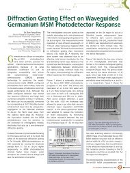
Diffraction Grating Effect on Waveguided<br />
Germanium MSM Photodetector Response<br />
Dr. Ren Fang-Fang<br />
Senior Research Engineer, Nano-<br />
Electronics and <strong>Photonics</strong> Programme<br />
Dr. Ang Kah-Wee<br />
Senior Research Engineer, Nano-<br />
Electronics and <strong>Photonics</strong> Programme<br />
Dr. Patrick Lo G. Q.<br />
Program Director, Nano-Electronics<br />
and <strong>Photonics</strong> Programme<br />
Germanium-on-silicon-on-insulator<br />
(Ge-on-SOI) photodetectors<br />
have been actively pursued for<br />
optical interconnection/communication<br />
applications because <strong>of</strong> its large<br />
absorption coefficient [1] and its<br />
integration compatibility with silicon<br />
(Si) complementary metal-oxidesemiconductor<br />
(CMOS) process<br />
technology. In particular, the metalsemiconductor-metal<br />
(MSM) configured<br />
photodiodes have been widely used due<br />
to its relative ease <strong>of</strong> fabrication and high<br />
speed performance [2,3]. Although the<br />
MSM configured detector may exhibit<br />
low quantum efficiency and large dark<br />
current as compared to the p-i-n detector,<br />
the latter can be successfully overcome<br />
by incorporating a Si:C Schottky-barrier<br />
enhancement layer [4] or by using sulfursegregation<br />
at the NiGe/Ge interface<br />
to de-pin the Fermi level away from<br />
the valence band edge [5]. However,<br />
the illumination incident into the MSM<br />
photodetectors may be sensitive to<br />
the dimension <strong>of</strong> interdigitated metallic<br />
electrodes that acts as a one-dimension<br />
diffraction grating.<br />
The interdigitated structure acted as the<br />
metallic electrodes and a one-dimensional<br />
(1D) metallic rectangular grating above the<br />
Ge active region. The measurements were<br />
operated at near-infrared wavelength <strong>of</strong><br />
1.55 µm under transverse magnetic (TM)<br />
mode, because TM mode is more sensitive<br />
to diffraction grating than transverse<br />
electric (TE) mode [6]. A relatively low<br />
dark current was observed due to an<br />
effective hole barrier modulation by the<br />
Si:C Schottky barrier layer. Based on the<br />
optical near-field simulation, we analyzed<br />
the relationship between photocurrent<br />
and optical energy confined inside the<br />
Ge region, demonstrating the diffraction<br />
effect induced by the metallic grating.<br />
Figure 1 shows a schematic structure<br />
<strong>of</strong> the Ge-on-SOI MSM photodetector<br />
proposed in this work. The device was<br />
fabricated on an 8-inch SOI wafer with<br />
a 2 µm thick buried oxide. Dry etching<br />
was used to form a Si waveguide 220<br />
nm in thickness and 500 nm in width.<br />
After active window definition, a pure<br />
Ge film with ~500 nm thickness was<br />
allowed to grow in an ultra-high vacuum<br />
chemical vapor deposition (UHVCVD)<br />
reactor. A thin silicon-germanium buffer<br />
was adopted to reduce the formation<br />
<strong>of</strong> misfit dislocations by minimizing<br />
the lattice mismatch between the two<br />
heterostructure materials [4]. A crystalline<br />
Si:C interfacial layer <strong>of</strong> ~20 nm was then<br />
deposited on the Ge region to act as a<br />
Schottky barrier enhancement layer<br />
for effective dark current reduction.<br />
Subsequently, the SiO 2<br />
passivation layer<br />
<strong>of</strong> 400nm was deposited and selectively<br />
dry etched to form contact hole. The<br />
metallization comprising <strong>of</strong> aluminum (Al)<br />
was deposited and patterned to complete<br />
the device fabrication.<br />
Figure 1(a) depicts the top-view scheme<br />
<strong>of</strong> the interdigitated electrodes that<br />
formed a 1D metallic rectangular grating<br />
as shown from the cross-sectional<br />
viewpoint [Figure 1(b)]. The groove depth<br />
was having the same thickness <strong>of</strong> Al<br />
layer, which was fixed at 400 nm in this<br />
experiment. The finger width, spacing and<br />
periodicity were indicated by w, s, and Λ=<br />
w + s, respectively. Figure 2 shows the<br />
Figure 2: Top-view SEM image <strong>of</strong> the Ge-on-<br />
SOI MSM photodetector featuring interdigitated<br />
electrodes with an effective device width W <strong>of</strong> 25<br />
µm and length L <strong>of</strong> 50 µm.<br />
To date, there are only few studies focusing<br />
on this issue and our aim is to study the<br />
effect <strong>of</strong> the electrode diffraction grating<br />
in Ge Schottky MSM photodetectors on<br />
SOI substrate by varying the electrode<br />
periods from 1.7, 1.8, to 1.9 µm. Higher<br />
responsivity in MSM photodetectors<br />
indicate higher noise margin, wider<br />
allowance for smaller device design and<br />
also the elimination <strong>of</strong> amplifier.<br />
Figure 1: Schematic illustration <strong>of</strong> the Ge-on-<br />
SOI MSM photodetector with interdigitated<br />
metal electrodes. (a) Top view <strong>of</strong> the<br />
interdigitated fingers. (b) Cross-sectional view<br />
<strong>of</strong> the device structure.<br />
top-view scanning electron microscopy<br />
(SEM) image <strong>of</strong> our fabricated Ge-on-SOI<br />
MSM detector structure with an effective<br />
device width W <strong>of</strong> 25 μm and a length L<br />
<strong>of</strong> 50 μm, respectively. Due to a difference<br />
in the refractive index between Si and Ge,<br />
the incidence photon traveling in the Si<br />
waveguide would be up-coupled into the<br />
Ge region for absorption.<br />
The photoresponse characteristics <strong>of</strong> the<br />
Ge-on-SOI MSM photodetectors were<br />
www.ime.a-star.edu.sg<br />
microE Bulletin | Issue 3 October 2009 11
R&D News<br />
By comparing Figure 5(a) with 5(b), the<br />
measured photocurrent showed good<br />
consistency with the simulated optical<br />
energy. The extent <strong>of</strong> confinement<br />
and resonant quality factor due to the<br />
diffraction effect was shown to exhibit<br />
strong dependence on the finger width<br />
geometry, which in turn resulted in a<br />
difference in the photon absorption. During<br />
the process <strong>of</strong> simulation, we assumed<br />
there were no optical absorption by the<br />
Ge layer so that we could estimate the<br />
optical energy inside the active region.<br />
Figure 3: Photoresponse characteristics <strong>of</strong> a Ge-on-SOI interdigitated MSM photodetector with finger<br />
width w <strong>of</strong> 1.2 μm and spacing s <strong>of</strong> 0.6 μm. The optical measurement was performed by injecting a<br />
TM-mode incident electromagnetic (EM) wave with a wavelength λ <strong>of</strong> 1.55 μm into the Si waveguide<br />
and coupled into the Ge active region for absorption. The responsivity <strong>of</strong> the detector was calculated by<br />
subtracting the waveguide transmission loss <strong>of</strong> ~3.5 dB/cm and a coupling loss <strong>of</strong> ~4.5 dB.<br />
plotted in Figure 3. The devices were<br />
featuring w <strong>of</strong> 1.2 μm and s <strong>of</strong> 0.6 μm. At<br />
an applied bias <strong>of</strong> 1.0 V, a low dark current<br />
<strong>of</strong> 0.5 μA (0.4 nA/μm²) was measured.<br />
This measurement was below the typical<br />
1.0 µA generally considered to be the<br />
upper limit for high speed receiver design<br />
and consistent with the previous reported<br />
value on MSM devices [3]. The optical<br />
measurement was performed by injecting<br />
a TM mode incident electromagnetic<br />
(EM) wave with a wavelength λ <strong>of</strong> 1.55<br />
µm into the Si waveguide and coupled<br />
into Ge active region for absorption. The<br />
incidence light power was estimated<br />
to be ~1 mW. At an applied bias <strong>of</strong> 1 V,<br />
the photocurrent was measured to be<br />
~1.51 mA. The responsivities were well<br />
demonstrated to be over 1 A/W.<br />
Figure 4: The normalized distribution <strong>of</strong> magnetic<br />
field under TM mode in a photodetector with finger<br />
width w <strong>of</strong> 1.2 µm and spacing s <strong>of</strong> 0.6 µm.<br />
12 <strong>Institute</strong> <strong>of</strong> <strong>Microelectronics</strong><br />
In order to evaluate the effect <strong>of</strong> the<br />
electrode diffraction grating on the<br />
response performance, the spatial<br />
distribution <strong>of</strong> the magnetic field in the<br />
structure based on the Finite-Difference<br />
Time-Domain method was calculated as<br />
shown in Figure 4, for a detector with a<br />
w <strong>of</strong> 1.2 μm and s <strong>of</strong> 0.6 μm. It was noted<br />
that the optical field appeared to be locally<br />
concentrated beneath the electrodes<br />
attributed to the diffraction grating effect<br />
<strong>of</strong> metallic electrodes.<br />
To further confirm the impact <strong>of</strong> the<br />
metallic grating, we compared the<br />
measurement and simulation results<br />
for samples with varied electrode width<br />
w <strong>of</strong> 1.2, 1.3, and 1.4 µm (period Λ<br />
corresponding to 1.7, 1.8, and 1.9 µm)<br />
under TM modes, as shown in Figure 5(a)<br />
and 5(b). The spacing width s was fixed<br />
at 0.5 μm to maintain the same lateral<br />
spacing between the two adjacent fingers.<br />
The other structural parameters such as l<br />
and g (refer to Figure 1) were designed<br />
to ensure the same order dark current<br />
density. Photocurrent measurements<br />
were performed at an applied bias <strong>of</strong><br />
1 V. In Figure 5(b), we integrated the<br />
optical energy localized in the whole Ge<br />
active layer for these three dimensions.<br />
Figure 5: Effects <strong>of</strong> the electrode diffraction<br />
grating on the detector’s photoresponse. (a) is the<br />
photocurrent measurement results at an applied<br />
bias <strong>of</strong> 1 V. (b) shows the calculated optical energy<br />
confinement within the Ge region.<br />
In summary, Schottky interdigitated<br />
Ge-on-SOI MSM photodetectors with<br />
various finger width were fabricated<br />
with low dark current leakage. The<br />
photoresponse exhibited strong<br />
dependence on the finger width geometry,<br />
and showed good consistency with<br />
the numerical simulation. The results<br />
imply that the occurrence <strong>of</strong> optical<br />
energy localization beneath the metallic<br />
electrodes is beneficial to achieve<br />
higher photoresponse, which allows<br />
simultaneous achievement <strong>of</strong> high-speed<br />
response and sufficient responsivity in a<br />
small semiconductor element.<br />
References<br />
[1]<br />
[2]<br />
[3]<br />
[4]<br />
[5]<br />
[6]<br />
R. A. Soref, Proc. IEEE, 81(12), 1687<br />
(1993).<br />
J. Oh, S. Csutak, and J. C. Campbell, IEEE<br />
Photon. Technol. Lett., 14, 369 (2002).<br />
K. W. Ang, S. Zhu, M. Yu, G. Q. Lo, and<br />
D. L. Kwong, IEEE Photon. Technol. Lett.,<br />
20(9), 754 (2008).<br />
K. W. Ang, S. Y. Zhu, J. Wang, K. T. Chua,<br />
M. B. Yu, G. Q. Lo, and D. L. Kwong, IEEE<br />
Elect. Dev. Lett., 29(7), 704 (2008).<br />
K. W. Ang, M. B. Yu, S.Y. Zhu, K. T. Chua,<br />
G. Q. Lo, and D. L. Kwong, IEEE Elect.<br />
Dev. Lett., 29(7), 708 (2008).<br />
A. S. Vengurlekar, Optics Lett., 33, 1669<br />
(2008).
Efficient silicon-based light<br />
source could enable full<br />
monolithically integrated photonic<br />
circuits leveraging on Si-CMOS<br />
technology [1-7]. However, the brightness<br />
<strong>of</strong> light emission from silicon-based<br />
materials is insufficient due to the low<br />
radiative recombination efficiency in the<br />
indirect-gap system. As an alternative<br />
approach, the <strong>Photonics</strong> team in IME<br />
designed and fabricated triangularlattice<br />
airhole photonic crystal patterns<br />
in the silicon rich oxide (SRO)/SiO 2<br />
multilayer stacks to improve the light<br />
extraction by providing a convenient<br />
way <strong>of</strong> redistribution the light energy<br />
in desired form and orientation<br />
[8-13]. As a result, the intensity and<br />
pr<strong>of</strong>ile <strong>of</strong> spontaneous emission<br />
were found to be efficiently modulated<br />
by controlling the optical modes via<br />
varying the structural dimensions<br />
<strong>of</strong> photonic crystals. With lattice<br />
constant/radius <strong>of</strong> 700 nm/280 nm, the<br />
roomtemperature photoluminescence<br />
intensity was enhanced up to ~9 times in<br />
the vertical direction. The mechanisms for<br />
different enhancement features have also<br />
been theoretically analyzed based on<br />
coherent scattering and quantum<br />
electrodynamic effects, well consistent<br />
with the experiment observation.<br />
R&D News<br />
Light Extraction Improvement from<br />
Si-based Multilayers with Photonic<br />
Crystal Patterns<br />
Dr. Yu Mingbin<br />
Member <strong>of</strong> Technical Staff, Nano-<br />
Electronics and <strong>Photonics</strong> Programme<br />
Dr. Ren Fang-Fang<br />
Senior Research Engineer, Nano-<br />
Electronics and <strong>Photonics</strong> Programme<br />
Figure 1: (a) Schematic diagram <strong>of</strong> the<br />
3D-confined structure. (b) X-TEM image <strong>of</strong><br />
the active region composed <strong>of</strong> ten periods<br />
<strong>of</strong> SRO/SiO 2<br />
multiple quantum well. (c) SEM<br />
top view <strong>of</strong> a 2D triangular-lattice air-hole<br />
photonic crystal (PC) geometry.<br />
(100) by plasmaenhanced chemical vapor<br />
deposition (PECVD) system using SiH 4<br />
and N 2<br />
O as the source gases. Figure 1(b)<br />
shows the cross-sectional transmission<br />
electron microscopy (X-TEM) <strong>of</strong> the<br />
SRO (~12.9nm)/SiO 2<br />
(~13.1nm) MQW<br />
layers. As shown in Figure 1(c), the<br />
top-view image <strong>of</strong> scanning electron<br />
microscope (SEM) exhibited the exact<br />
regular 2D triangular-lattice air-hole PC<br />
geometry, which was fabricated by dry<br />
etching <strong>of</strong> the upper cladding down<br />
through the entire active region with the<br />
etching depth <strong>of</strong> h = 300 nm. The lattice<br />
constant and the radius were labeled as a<br />
and r, and thus the duty cycle <strong>of</strong> air holes<br />
was described as 2πρ 2 √¯3 , here ρ = r / a .<br />
Two groups <strong>of</strong> PC patterns (A-B and<br />
C-E) were fabricated and tested with<br />
various lattice constants and duty cycles,<br />
as listed in Table I. All fabricated samples<br />
were annealed at 900 o C for 30 minutes<br />
in N 2<br />
-ambient to enhance the internal<br />
light emission efficiency.<br />
The photoluminescence (PL) spectra<br />
were collected at room temperature using<br />
a Renishaw Micro-PL system with the<br />
excitation source <strong>of</strong> He-Cd laser (325 nm)<br />
and the incident power <strong>of</strong> ~1 mW. The light<br />
emissions were recorded for wavelength<br />
<strong>of</strong> 400-900 nm by the liquid-N 2<br />
cooled<br />
CCD system in the vertical direction<br />
through the microscope. Figure 2 shows<br />
the PL emissions from the patterned<br />
regions A-E, and from an unpatterned<br />
region as reference. To illustrate the<br />
enhancement features, the PL intensities<br />
have been normalized to the effective<br />
area <strong>of</strong> the active material (1 – 2πρ 2 √¯3) for<br />
each pattern. The light emission around<br />
620 nm dominated the spectrum <strong>of</strong> the<br />
unpatterned region and appeared in the<br />
patterned areas without discernable shift,<br />
which was originated from the vertical<br />
quantum confinement effect in the MQW<br />
layers. The significant enhancements <strong>of</strong><br />
light emissions were observed around<br />
720 nm from all the patterned regions,<br />
but the enhancement magnitudes and<br />
peak positions were strongly dependent<br />
on the lattice constants and duty cycles.<br />
Figure 1(a) shows the schematic <strong>of</strong> the<br />
patterned structure. The upper and lower<br />
claddings were Si 3<br />
N 4<br />
and SiO 2<br />
with<br />
thickness <strong>of</strong> 50 and 150 nm, respectively.<br />
A 10-period thin SRO/SiO 2<br />
multilayer<br />
stack acted as the light emitting source<br />
with vertical quantum confinement in<br />
SRO well layers. These multilayers were<br />
deposited sequentially on silicon substrate<br />
Table 1: Structural parameters <strong>of</strong> patterns A-E<br />
microE Bulletin | Issue 3 October 2009 13
R&D News<br />
Especially, for the pattern E with a=700<br />
nm and ρ=0.40, the spectral integrated<br />
PL intensity in the vertical direction was<br />
boosted up to 9 folds, indicating that such<br />
2D PC arrays had a large impact on the<br />
output <strong>of</strong> the spontaneous emission. The<br />
exact origin <strong>of</strong> such enhancement features<br />
Figure 2: PL spectra recorded in the vertical<br />
direction at room temperature for patterns A-E<br />
and an unpatterned region.<br />
could be well explained theoretically<br />
based on the band structure modulation<br />
<strong>of</strong> 2D PC slabs.<br />
In this study, a non-linear equation<br />
method based on plane-wave expansion<br />
was employed to calculate the band<br />
structures <strong>of</strong> PC patterns [14-16]. Here,<br />
only the results for pattern E (a=700 nm,<br />
ρ=0.40) is shown in Figure 3.<br />
Figure 3: The photonic band diagrams for phonic<br />
crystal slabs with pattern E (a=700 nm, ρ=0.40).<br />
Results<br />
As shown in Figure 2, the PL intensities<br />
from patterns with a=700 nm (C, D and<br />
E) were much stronger than those from<br />
patterns with a=400 nm (A and B), which<br />
indicated that the enhancement factor<br />
<strong>of</strong> emission was primarily influenced by<br />
the variation <strong>of</strong> lattice constant rather<br />
than duty cycle in the tested range. In the<br />
case <strong>of</strong> pattern E (a=700 nm, ρ=0.40), the<br />
PL peak around 694 nm corresponded to<br />
the normalized frequency a / λ = 1.0, near<br />
the ρ point <strong>of</strong> the TE-like leaky conduction<br />
band (indicated by arrow) in Figure 3. The<br />
light generated thus strongly coupled with<br />
the high-Q (quality factor) leaky modes [8]<br />
and eventually escaped into free space<br />
from the slab in the vertical direction<br />
[13, 15]. Based on the same mechanism,<br />
PL intensities <strong>of</strong> the regions with patterns<br />
C (a=700 nm, ρ=0.25) and D (a=700 nm,<br />
ρ=0.35) were also greatly improved. As<br />
for patterns A (a=400 nm, ρ=0.35) and<br />
B (a=400 nm, ρ=0.40), the PL intensities<br />
exhibited about 2 -3× enhancement over<br />
the reference, mainly within the range<br />
<strong>of</strong> 550-800 nm. The corresponding<br />
optical modes <strong>of</strong> PC slab move to the<br />
lower normalized frequencies from about<br />
0.5 to 0.73 due to the smaller constant<br />
lattice compared with C, D and E, which<br />
overlapped with the photonic band gap<br />
(PBG) region and the TM-like resonant<br />
radiation band (not shown).<br />
We therefore speculated that the<br />
enhancement in this case was mainly due<br />
to two possible mechanisms. First <strong>of</strong> all,<br />
since the lateral propagation <strong>of</strong> guided<br />
modes in PBG region was prohibited<br />
in the slab, light generated could only<br />
radiate in the vertical direction, which<br />
was described as the redistribution <strong>of</strong><br />
saved energy by PBG effect [17]. Secondly,<br />
the light emission corresponding to<br />
TM-like guided modes was folded to<br />
high-Q resonant radiation modes at<br />
the Brillouin zone boundaries by phase<br />
compensation from a reciprocal lattice<br />
vector, thus leading to higher external<br />
quantum efficiencies [10]. The relatively<br />
small enhancement factor observed was<br />
partially due to the inhibition <strong>of</strong><br />
recombination <strong>of</strong> excited carriers in the<br />
in-plane direction by PBG effect [13].<br />
With the radius <strong>of</strong> air hole being increased<br />
from C, D to E, the significant PL peak<br />
exhibited blue-shift from 750 to 694<br />
nm. Similar phenomena also occur in<br />
the cases <strong>of</strong> patterns A and B. That was<br />
because the effective refractive index <strong>of</strong><br />
PC slab decreased with the increasing<br />
<strong>of</strong> duty cycle while maintaining the<br />
lattice constant and slab depth, which<br />
consequently resulted in the blue-shift<br />
<strong>of</strong> photonic band structures [15]. When<br />
the value <strong>of</strong> ρ was reduced down to 0.25<br />
in pattern C, the states around K point<br />
lying in the conduction band would fall<br />
outside the light cone and become guided<br />
modes, which might be responsible for<br />
the smaller enhancement compared with<br />
D and E.<br />
Although the active material was partially<br />
removed by the dry etching process,<br />
spontaneous emission could also be<br />
compensated through two beneficial ways<br />
dominated by quantum electrodynamic<br />
effects. The first was the so-called Purcell<br />
spontaneous emission rate enhancement<br />
occurring in the wavelength-size cavities<br />
<strong>of</strong> PC, due to the high quality factor<br />
and small mode volume [16]. The second<br />
was the redistribution <strong>of</strong> pump energy in<br />
the active region. As an example, we<br />
calculated the electromagnetic (EM) field<br />
distribution <strong>of</strong> pump light (325 nm) in the<br />
plane <strong>of</strong> h/2 for the sample with pattern<br />
E, based on the Rigorous Coupled<br />
Wave Analysis (RCWA) method [18]. The<br />
image had been chosen as the cover<br />
image for Applied Physics Letters (Vol. 93,<br />
Issue 9) (Figure 4). From the electric and<br />
magnetic fields distribution, we could<br />
clearly notice that most <strong>of</strong> the energy was<br />
concentrated in the dielectric material<br />
region outside the air holes, thus provide<br />
Figure 4: The normalized electric and magnetic field<br />
intensity distribution <strong>of</strong> excitation incidence (325<br />
nm) in the plane <strong>of</strong> h/2 for the sample with pattern<br />
E. This was published on the cover page <strong>of</strong> Applied<br />
Physics Letters (Vol. 93, Issue 9).<br />
14 <strong>Institute</strong> <strong>of</strong> <strong>Microelectronics</strong>
R&D News<br />
magnified pump power intensities for<br />
spontaneous emission.<br />
Starting from 2006, the <strong>Photonics</strong> team<br />
made significant progress in Si-based<br />
light emission (as shown in Figure 5).<br />
Good PL and EL (Electroluminescence)<br />
performance from amorphous Si and<br />
PL from erbium (Er) doped materials<br />
were demonstrated over the visible or<br />
infrared communication wavelength<br />
range, which provide a potential platform<br />
for the integrated solution application.<br />
Figure 5: IME Roadmap for Si and Er based Emission<br />
References<br />
[1]<br />
[2]<br />
[3]<br />
[4]<br />
[5]<br />
[6]<br />
[7]<br />
[8]<br />
[9]<br />
L. T. Canham, Appl. Phys. Lett. 57, 1046 (1990).<br />
A. Polman, Nat. Mater. 1, 10 (2002).<br />
R. J. Walters, G. I. Bourian<strong>of</strong>f, and H. A. Atwater, Nat. Mater. 4, 143<br />
(2005).<br />
I. Bineva, D. Nesheva, Z. Aneva, and Z. Levi, J. Lumin. 126, 497<br />
(2007).<br />
W. K. Tan, M. B. Yu, Q. Chen, J. D. Ye, G. Q. Lo, and D. L. Kwong,<br />
Appl. Phys. Lett. 90, 221103 (2007).<br />
A. Morales-Sánchez, J. Barreto, C. Domínguez-Horna, M. Aceves-<br />
Mijares, and J. A. Luna-López, Sens. Actuat. A 142, 12 (2008).<br />
M. H. Wang, D. R. Yang, D. S. Li, Z. Z. Yuan, and D. L. Que, J. Appl.<br />
Phys. 101, 103504 (2007).<br />
M. Boroditsky, T. F. Krauss, R. Coccioli, R. Vrijen, R. Bhat, and E.<br />
Yablonovitch, Appl. Phys. Lett. 75, 1036 (1999).<br />
S. Fan, P. R. Villeneuve, J. D. Joannopoulos, and E. F. Schubert,<br />
Phys. Rev. Lett. 78, 3294 (1997).<br />
[10] A. A. Erchak, D. J. Ripin, S. Fan, P. Rakich, J. D. Joannopoulos, E. P.<br />
Ippen, G. S. Petrich, and L. A. Kolodziejski, Appl. Phys. Lett. 78, 563<br />
(2001).<br />
[11] J. Y. Kim, M. K. Kwon, K. S. Lee, S. J. Park, S. H. Kim, and K. D. Lee,<br />
Appl. Phys. Lett. 91, 181109 (2007).<br />
[12] S. H. Kim, K. D. Lee, J. Y. Kim, M. K. Kwon, and S. J. Park,<br />
Nanotechnology 18, 055306 (2007).<br />
[13] H. Y. Ryu, Y. H. Lee, R. L. Sellin, and D. Bimberg, Appl. Phys. Lett. 79,<br />
3573 (2001).<br />
[14] D. S. Gao and Z. P. Zhou, Appl. Phys. Lett. 88, 163105 (2006).<br />
[15] S. G. Johnson, S. Fan, P. R. Villeneuve, J. D. Joannopoulos, and L. A.<br />
Kolodziejski, Phys. Rev. B 60, 5751 (1999).<br />
[16] M. Boroditsky, R. Vrijen, T. F. Krauss, R. Coccioli, R. Bhat, and E.<br />
Yablonovitch, J. Lightwave Technol. 17, 2096 (1999).<br />
[17] S. Noda, M. Fujita, and T. Asano, Nat. <strong>Photonics</strong> 1, 449 (2007).<br />
[18] E. Noponen and J. Turunen, J. Opt. Soc. Am. A 11, 2494 (1994).<br />
www.ime.a-star.edu.sg<br />
microE Bulletin | Issue 3 October 2009 15
Industry<br />
Collaboration<br />
Bell Laboratories, Alcatel-Lucent<br />
Bell Laboratories began to work with IME in September 2008 to<br />
realize a siliconbased coherent optical receiver on a single chip.<br />
Dr. Young-Kai Chen<br />
Director <strong>of</strong> High<br />
Speed Electronics and<br />
Optoelectronics Research,<br />
Bell Laboratories<br />
On 15 th June 2009, the <strong>Institute</strong> <strong>of</strong> <strong>Microelectronics</strong> and<br />
Bell Labs, the central research and development division<br />
<strong>of</strong> Alcatel-Lucent, signed a research collaboration<br />
agreement to jointly develop advanced photonics technology<br />
for next generation cost-effective high data-rate communication<br />
networks. The Editorial Team took this opportunity to interview<br />
Dr. Young-Kai Chen, Director <strong>of</strong> High Speed Electronics and<br />
Optoelectronics Research at the Bell Laboratories on his vision<br />
for the project and the partnership.<br />
“The joint research project with IME is to investigate advanced<br />
silicon photonic circuits. <strong>Silicon</strong> photonic circuit is a low cost and<br />
high functionality solution for future optic fiber communication<br />
systems to transport high capacity data and multi-media<br />
contents. The CMOS fabrication technology today is able to<br />
delineate features with dimensions below the commonly used<br />
wavelengths in optical communications. It will be promising to<br />
integrate the optical elements on the CMOS electronics platform<br />
for added intelligence and functionalities at a lower cost.” said<br />
Dr. Chen.<br />
He continued, “Bell Laboratories is exploring several areas to<br />
provide our customers with cost effective infrastructure products<br />
for optic fiber data links and fiber at their homes. Our initial<br />
objective was to explore the speed limit <strong>of</strong> the silicon photonics<br />
technology and we achieved the next generation optic fiber<br />
communications at 100 Gb/s. This result is very promising as<br />
it enables many new applications in delivering high speed data<br />
and multimedia contents to our customers in a “green” and cost<br />
effective manner.”<br />
“The result is amazing.” Dr Chen disclosed, “The team achieved a<br />
world-record data rate <strong>of</strong> 112 Gb/s which is ten-times faster than<br />
the current optical receivers being used in today’s back-bone<br />
optic fiber networks. The device integrates many functions<br />
such as polarization beam splitter, precision optical mixers<br />
and balanced photodetector array on a single chip to receive<br />
and decode received optical signals with complex modulated<br />
signaling format.” The record is reported in the post-deadline<br />
session <strong>of</strong> the Optical Fiber Communication Conference in April<br />
2009 and Bell Laboratories is continuing to work with IME to<br />
investigate new silicon photonic devices and circuits as well as<br />
to explore the manufacturing capability <strong>of</strong> the technology in the<br />
next phase <strong>of</strong> the collaboration.<br />
On the working relationship with IME, Dr. Chen revealed, “We are<br />
aware <strong>of</strong> IME’s <strong>of</strong>ferings in silicon photonics foundry. IME has<br />
excellent semiconductor researchers and fabrication facilities<br />
which have successfully powered Singapore’s semiconductor<br />
industry over the past few decades. Their close collaborations<br />
with the local foundries are definitely a very good path for future<br />
ramp up in manufacturing for our joint project.” Dr. Chen went<br />
on, “Researchers at IME provide excellent knowledge and<br />
timely feedback on our proposed advanced components and<br />
processes such that we have fully functional devices and circuits<br />
from the first pass <strong>of</strong> the fabrication. We are very impressed by<br />
the “can-do” attitude <strong>of</strong> IME’s researchers. Despite the 12-hours<br />
difference between our time zones, we were able to carry our<br />
conference calls in late evenings and even weekends on both<br />
sides and got the problem resolved within 24 hours.”<br />
“This successful research collaboration with IME has<br />
demonstrated and realized many advantages <strong>of</strong> our open<br />
research initiative at Alcatel-Lucent. By leveraging on the global<br />
expertise <strong>of</strong> the joint Bell Labs-IME team, we are able to carry<br />
out state-<strong>of</strong>-the-art research in a timely and effective manner.<br />
Bell Laboratories is very pleased to participate in developing the<br />
next generation silicon photonics technology in Singapore.”<br />
16 <strong>Institute</strong> <strong>of</strong> <strong>Microelectronics</strong>
Industry<br />
Collaboration<br />
Unisantis Electronics (Japan) Ltd.<br />
We at Unisantis are now engaged in the prototyping <strong>of</strong><br />
Surrounding Gate Transistor (SGT) with IME. The collaboration<br />
with IME aims to develop the basic process technology <strong>of</strong> SGT<br />
and to overcome the limitations <strong>of</strong> existing planar technology<br />
(as defined by Moore’s Law) by shrinking the chip size. This will<br />
be realized by shrinking the occupied area <strong>of</strong> the transistor and<br />
creation <strong>of</strong> an integrated circuit using such three dimensional<br />
transistors. With IME’s technical expertise in integrated circuits<br />
and their excellent integrated process capabilities, I am confident<br />
<strong>of</strong> achieving our mission.<br />
Q: What are the results <strong>of</strong> the collaboration and how<br />
will this invention change or impact end users?<br />
Pr<strong>of</strong>essor Fujio Masuoka<br />
Chief Technology Officer,<br />
Unisantis Electronics (Japan) Ltd.<br />
Unisantis Electronics (Japan) Ltd., is part <strong>of</strong> Newscope<br />
Group Holdings AG. The NewScope Group is a science<br />
and innovation driven conglomerate with widely diversified<br />
individual technology businesses and activities including<br />
design, research, development, manufacturing, marketing, and<br />
supplying innovative products. Unisantis Electronics (Japan) Ltd<br />
was established in 2004 and, under the leadership <strong>of</strong> its CTO<br />
Pr<strong>of</strong>essor Fujio Masuoka, is engaged in the development <strong>of</strong> a<br />
new three dimensional (3-D) transistor called the Surrounding<br />
Gate Transistor (SGT).<br />
In Dec 2007, Unisantis Electronics and IME inked a research<br />
collaboration agreement to jointly develop the SGT in Singapore,<br />
marking the beginning <strong>of</strong> the 24 months journey aimed at<br />
transforming the technological world. In this month’s exclusive<br />
interview, MicroE editorial team takes you behind the scene <strong>of</strong><br />
the development <strong>of</strong> the world’s first 3-D transistor with the man<br />
behind this astonishing invention, Pr<strong>of</strong>essor Fujio Masuoka.<br />
Q: What are the motivating factors for the project<br />
collaboration?<br />
Pr<strong>of</strong>. Masuoka: The Semiconductor industry has grown with<br />
“micronization” over the past 50 years and it is well known and<br />
acknowledged that “micronization” will soon reach its physical<br />
limits. I believe that a structural change <strong>of</strong> the transistor from<br />
planar to three dimensional will provide a solution to this<br />
challenging issue.<br />
Pr<strong>of</strong>. Masuoka: I am pleased and proud that the collaboration<br />
team is progressing much ahead <strong>of</strong> their schedule and will be<br />
embarking on the new phase <strong>of</strong> the collaboration with IME<br />
for further development <strong>of</strong> SGT technology. I believe that our<br />
collaborative efforts with IME will take successful shape and will<br />
bring plenty <strong>of</strong> chances to generate inventive patents related<br />
to SGT. We are also calling out to all capable and ambitious<br />
researchers to join us and be part <strong>of</strong> the team responsible in<br />
changing the world with SGT.<br />
The industry is poised to experience a major milestone upon<br />
successful completion <strong>of</strong> the project. The SGT will create a<br />
global impact and will change the way many technologies work.<br />
First and foremost, SGT will enable higher processing speeds<br />
and higher image resolution on computers. Researchers will be<br />
able to carry out most <strong>of</strong> their work on their own workstations in<br />
real time instead <strong>of</strong> depending on advanced computing facilities.<br />
With increased speeds, SGT can be used to screen new drugs<br />
for life threatening diseases in Biomedical research, to achieve<br />
faster and accurate mapping <strong>of</strong> DNA in Genome Research,<br />
for faster generation <strong>of</strong> weather forecasting models in Climate<br />
research, and to attain complex designs in the Aircraft and<br />
Automobile industries. The potential applications <strong>of</strong> SGT are vast<br />
and boundless.<br />
Q: How was your experience in the collaboration<br />
with IME?<br />
Pr<strong>of</strong>. Masuoka: The IME research team has lived up to the<br />
challenges <strong>of</strong> this unique development and had consistently<br />
contributed at a superior level throughout the course <strong>of</strong> the joint<br />
project. From the planning to the development stage, the IME<br />
team has demonstrated their high enthusiasm and passion in the<br />
development <strong>of</strong> the SGT. I am very pleased and satisfied with<br />
their work, attitude, excellent skill levels and cooperation.<br />
www.ime.a-star.edu.sg<br />
microE Bulletin | Issue 3 October 2009 17
People<br />
IME is indeed an excellent training<br />
place for researchers and engineers<br />
specializing in semiconductor<br />
research.<br />
Zhao Hui<br />
a former PhD student attached to IME.<br />
Graduated recently from the National University <strong>of</strong><br />
Singapore (NUS), Zhao Hui is one <strong>of</strong> the pool <strong>of</strong> students<br />
who have pursued their PhD project in a research<br />
institute through A*STAR research attachment programme. She<br />
was attached to IME’s Nano-Electronics & <strong>Photonics</strong> (NanoEP)<br />
Programme for three years under the Joint <strong>Microelectronics</strong><br />
Laboratory (JML) scheme from the Department <strong>of</strong> Electrical and<br />
Computer Engineering.<br />
When the editorial team caught up with the young post graduate,<br />
she was all perky and excited about the interview. The bubbly<br />
graduate was fast to get down to the interview and quipped, “The<br />
attachment opportunity in IME was arranged by my university’s<br />
supervisor but the main motivation factors for me were its first<br />
class facilities and expertise in the field <strong>of</strong> nan<strong>of</strong>abrication.”<br />
Zhao Hui recently joined one <strong>of</strong> the largestelectronic design<br />
automation (EDA) company for IC industry, Synopsys, as a<br />
Corporate Application Engineer. Looking back on her attachment<br />
in IME, she said, “I had gained and picked up important technical<br />
knowledge from my attachment in IME. I was given opportunities<br />
to propose and test out my ideas through experiments with the<br />
comprehensive facilities in the institute. These had given me<br />
invaluable hands-on experience <strong>of</strong> the equipment and processes<br />
in nano device fabrication.”<br />
Zhao Hui was working on the design, fabrication and characterization<br />
<strong>of</strong> Nanowire devices during her attachment. “I<br />
had simulated, designed, and fabricated the test keys for<br />
femto-farad nanowire capacitance measurement. The fabricated<br />
devices were used for measurement <strong>of</strong> current and capacitance.<br />
Series resistance and carrier mobility were then extracted for<br />
further device study”, she disclosed. Under the guidance <strong>of</strong> Dr.<br />
Subhash, Zhao Hui’s research work on “CBCM Measurement <strong>of</strong><br />
Femto-Farad Nanowire Capacitance” was published in IEDM<br />
2008. This is the first demonstration <strong>of</strong> a single channel silicon<br />
nanowire capacitance and mobility extraction. “It provides a very<br />
simple and innovative approach to measuring extremely small<br />
capacitances accurately. I am very proud and pleased <strong>of</strong> the<br />
result and I want to thank the team for their contribution”, Zhao<br />
Hui continued.<br />
”My supervisor at IME was Dr. Subhash Chander and I could<br />
not wish for any better or friendlier supervisor than him. Apart<br />
from his expertise in modeling and characterization, he is<br />
also a very patient and bighearted mentor. His generosity in<br />
sharing his knowledge and patience helped me most during<br />
my attachment. As a very hands-on person, he would sit down<br />
with us to brainstorm, whenever we experience any difficulties<br />
in the research work. Through his guidance, I learnt that to be<br />
an outstanding researcher, apart from overcoming the technical<br />
challenges, it also involving prioritizing, working in a team and<br />
managing stress. I am extremely fortunate to work with IME and<br />
Dr. Subhash over the past 3 years. It is an experience I would<br />
cherish forever.”<br />
18 <strong>Institute</strong> <strong>of</strong> <strong>Microelectronics</strong>
People<br />
Similarly, Jiang Yu, a former PhD student from the Electrical<br />
and Computer Engineering department, National University<br />
<strong>of</strong> Singapore, was attached to IME for her research work,<br />
through the A*STAR Joint <strong>Microelectronics</strong> Laboratory scheme.<br />
She was attached to IME’s Nano-Electronics & <strong>Photonics</strong><br />
(NanoEP) Programme, under the mentorship <strong>of</strong> Pr<strong>of</strong>. Kwong<br />
Dim-Lee.<br />
Known as a pleasant and outstanding student, Jiang Yu’s<br />
research focus was on exploring solutions for advanced high<br />
performance nanowire transistors. On her view about IME,<br />
Jiang Yu commented, “IME possesses advance research and<br />
semiconductor device fabrication facilities. It is full <strong>of</strong> experts and<br />
senior engineers in many diverse research fields. The research<br />
atmosphere in IME is very active. The environment promotes<br />
constructive discussions between fellow attached students and<br />
its research staffs. The research topics <strong>of</strong>fered by IME are both<br />
attractive and interesting and the focus on staying relevant to<br />
the industry brings significant worth to researchers’ work and<br />
publications. IME has a conducive environment for students to<br />
learn and the opportunity to work as part <strong>of</strong> the team.”<br />
During her attachment, Jiang Yu had presented 4 papers in<br />
prestigious international conferences. Of these, 2 papers were<br />
published in VLSI 2008 and IEDM 2008, the top conferences in<br />
her research field. One <strong>of</strong> her papers was awarded the Maruban<br />
Foundation Award in SSDM 2007, while another was selected as<br />
one <strong>of</strong> the technical highlights in SSDM 2008. Jiang Yu has filed<br />
a patent for high speed SiGe nanowire transistors.<br />
On her mentor, she said, “Pr<strong>of</strong>. Kwong was a really nice supervisor<br />
to work with. I remember the first time I met Pr<strong>of</strong>. Kwong. He<br />
was very friendly and provided many valuable suggestions and<br />
options on the selection <strong>of</strong> my research topic. He wanted me to<br />
know and understand my options before making a choice. I am<br />
very grateful to him as I was able to work on a research topic that<br />
I had keen interest in. This approach enticed my commitment to<br />
the research. On top <strong>of</strong> that, Pr<strong>of</strong>. Kwong encouraged me to read<br />
at least one journal paper each day, which he practices despite<br />
his busy work schedule. He trained my analytical skills and my<br />
ability to work independently.”<br />
“IME had prepared me well for a career in R&D. The institute has<br />
many experts in the different research fields and I was always<br />
able to find experts like Dr. Patrick Lo, Dr. Navab Singh and<br />
many other module engineers to discuss my work at the different<br />
stages <strong>of</strong> my research. Besides technical, I learned to work in a<br />
team. I would not have gained such valuable experiences from<br />
the university environment. IME has indeed helped in preparing<br />
me for the R&D workforce.”<br />
Jiang Yu is currently a researcher with Unisantis Electronics<br />
(Japan) Ltd., one <strong>of</strong> IME’s most valuable R&D partners. IME and<br />
Unisantis are in a partnership to jointly develop the Surrounding<br />
Gate Transistor (SGT) in Singapore and Jiang Yu is part <strong>of</strong> the<br />
team working on the project.<br />
Jiang Yu shared further, “My goal is to become a world-class<br />
researcher and I hope to be able to contribute significantly in the<br />
field <strong>of</strong> semiconductor devices.”<br />
The research atmosphere in<br />
IME is really active and promotes<br />
constructive discussions between<br />
fellow attached students and its<br />
research staffs.<br />
Jiang Yu<br />
PhD graduate from NUS<br />
Successful Master/PhD applicants with NTU or NUS as well as AGS scholars who are<br />
interested to conduct their graduate research work in our young and vibrant research<br />
atmosphere, please write to uni-collaboration@ime.astar.edu.sg.<br />
microE Bulletin | Issue 3 October 2009 19
SUBSCRIBE TODAY<br />
E<br />
Flash<br />
bi-yearly issue<br />
monthly e-newsletter (digital only)<br />
To qualify for the subscription <strong>of</strong> IME’s MicroE Bulletin and eFlash newsletter, please complete the<br />
form below. Incomplete forms will not be processed.<br />
Do you wish to receive / continue to receive Free subscription <strong>of</strong> MicroE Bulletin?<br />
Yes [ ] New [ ] Renew<br />
No<br />
Do you wish to receive monthly IME e-newsletter eFlash (Digital only)?<br />
Yes [ ] New [ ] Renew<br />
No<br />
MAIL THIS FORM<br />
TO:<br />
Editorial Team<br />
<strong>Institute</strong> <strong>of</strong><br />
<strong>Microelectronics</strong><br />
11 Science Park Road<br />
Singapore Science Park II<br />
Singapore 117685<br />
OR<br />
SEND IT TO:<br />
editorial@ime.a-star.edu.sg<br />
X<br />
Signature (Required)<br />
Email Address<br />
Tel<br />
Fax<br />
Reader’s Information<br />
First Name<br />
Job Title<br />
Company Name<br />
Address<br />
Date<br />
Last Name<br />
Department<br />
City<br />
State<br />
Country<br />
Postal Code