8086 Microprocessor (cont..) - nptel
8086 Microprocessor (cont..) - nptel
8086 Microprocessor (cont..) - nptel

You also want an ePaper? Increase the reach of your titles
YUMPU automatically turns print PDFs into web optimized ePapers that Google loves.
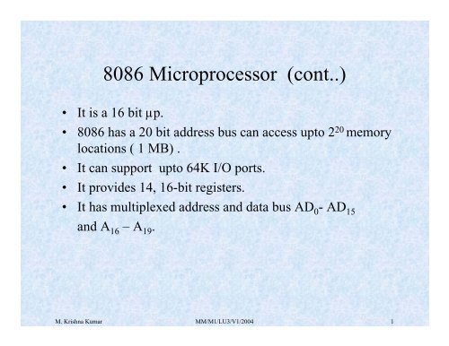
<strong>8086</strong> <strong>Microprocessor</strong> (<strong>cont</strong>..)<br />
• It is a 16 bit µp.<br />
• <strong>8086</strong> has a 20 bit address bus can access upto 2 20 memory<br />
locations ( 1 MB) .<br />
• It can support upto 64K I/O ports.<br />
• It provides 14, 16-bit registers.<br />
• It has multiplexed address and data bus AD 0 -AD 15<br />
and A 16 –A 19 .<br />
M. Krishna Kumar MM/M1/LU3/V1/2004 1
<strong>8086</strong> <strong>Microprocessor</strong> (<strong>cont</strong>..)<br />
• It requires single phase clock with 33% duty cycle to<br />
provide internal timing.<br />
• <strong>8086</strong> is designed to operate in two modes, Minimum and<br />
Maximum.<br />
• It can prefetches upto 6 instruction bytes from memory and<br />
queues them in order to speed up instruction execution.<br />
• It requires +5V power supply.<br />
• A 40 pin dual in line package.<br />
M. Krishna Kumar MM/M1/LU3/V1/2004 2
<strong>8086</strong> <strong>Microprocessor</strong> (<strong>cont</strong>..)<br />
Minimum and Maximum Modes:<br />
• The minimum mode is selected by applying logic 1 to the<br />
MN / MX# input pin. This is a single microprocessor<br />
configuration.<br />
• The maximum mode is selected by applying logic 0 to the<br />
MN / MX# input pin. This is a multi micro processors<br />
configuration.<br />
M. Krishna Kumar MM/M1/LU3/V1/2004 3
<strong>8086</strong> <strong>Microprocessor</strong> (<strong>cont</strong>..)<br />
GENERAL<br />
REGISTERS<br />
AH<br />
BH<br />
CH<br />
DH<br />
SP<br />
BP<br />
SI<br />
DI<br />
AL<br />
BL<br />
CL<br />
DL<br />
∑<br />
ADDRESS BUS<br />
( 20 )<br />
BITS<br />
DATA BUS<br />
( 16 )<br />
BITS<br />
ES<br />
CS<br />
SS<br />
ALU DATA BUS<br />
16 BITS<br />
DS<br />
IP<br />
BUS<br />
8<br />
0<br />
8<br />
TEMPORARY REGISTERS<br />
CONTROL<br />
LOGIC<br />
6<br />
B<br />
U<br />
S<br />
ALU<br />
EU<br />
CONTROL<br />
SYSTEM<br />
Q BUS<br />
1<br />
INSTRUCTION QUEUE<br />
2 3 4 5 6<br />
8 BIT<br />
FLAGS<br />
BUS INTERFACE UNIT ( BIU)<br />
EXECUTION UNIT ( EU )<br />
Fig:<br />
M. Krishna Kumar MM/M1/LU3/V1/2004 4
Pin Diagram of <strong>8086</strong><br />
GND<br />
AD 14<br />
AD 13<br />
AD 12<br />
AD 11<br />
AD 10<br />
AD 9<br />
AD 8<br />
AD 7<br />
AD 6<br />
AD 5<br />
AD 4<br />
AD 3<br />
AD 2<br />
AD 1<br />
AD 0<br />
NMI<br />
INTR<br />
CLK<br />
GND<br />
1<br />
2<br />
3<br />
4<br />
5<br />
6<br />
7<br />
8<br />
9<br />
10<br />
11<br />
12<br />
13<br />
14<br />
15<br />
16<br />
17<br />
18<br />
19<br />
20<br />
<strong>8086</strong><br />
CPU<br />
40<br />
39<br />
38<br />
37<br />
36<br />
35<br />
34<br />
33<br />
32<br />
31<br />
30<br />
29<br />
28<br />
27<br />
26<br />
25<br />
24<br />
23<br />
22<br />
21<br />
V CC<br />
AD 15<br />
A 16 / S 3<br />
A 17 / S 4<br />
A 19 /S 6<br />
____<br />
___<br />
MN/MX<br />
RD<br />
___ _____ RQ / GT 0<br />
( HOLD)<br />
RQ / GT 1<br />
( HLDA)<br />
_______<br />
LOCK<br />
___<br />
S___<br />
1<br />
______<br />
TEST<br />
READY<br />
RESET<br />
_____<br />
___<br />
(WR)<br />
A 18 / S 5<br />
_____<br />
BHE / S 7<br />
_____ _____<br />
___<br />
(DT / R)<br />
____<br />
S 2<br />
S 0 (DEN)<br />
________ QS 0<br />
QS 1 (INTA)<br />
(ALE)<br />
____<br />
(M / IO )<br />
M. Krishna Kumar MM/M1/LU3/V1/2004 5
V CC<br />
<strong>8086</strong><br />
GND<br />
A 0<br />
- A15, A 16<br />
/ S 3<br />
–A 19<br />
/S 6<br />
INTR<br />
_____<br />
INTA<br />
______<br />
TEST<br />
INTERRUPT<br />
INTERFACE<br />
ADDRESS / DATA BUS<br />
D 0<br />
- D 15<br />
NMI<br />
RESET<br />
MPU<br />
ALE<br />
___<br />
BHE / S 7<br />
__<br />
HOLD<br />
HLDA<br />
V CC<br />
____<br />
MN / MX<br />
DMA<br />
INTERFACE<br />
MODE<br />
SELECT<br />
MEMORY<br />
I / O<br />
CONTROLS<br />
M / IO<br />
____<br />
RD<br />
_____<br />
WR<br />
_____<br />
DEN<br />
READY<br />
__<br />
DT / R<br />
CLK<br />
M. Krishna Kumar MM/M1/LU3/V1/2004 6
Internal Architecture of <strong>8086</strong><br />
• <strong>8086</strong> has two blocks BIU and EU.<br />
• The BIU performs all bus operations such as instruction<br />
fetching, reading and writing operands for memory and<br />
calculating the addresses of the memory operands.<br />
• The instruction bytes are transferred to the instruction<br />
queue.<br />
• EU executes instructions from the instruction system byte<br />
queue.<br />
M. Krishna Kumar MM/M1/LU3/V1/2004 7
Internal Architecture of <strong>8086</strong> (<strong>cont</strong>..)<br />
• Both units operate asynchronously to give the <strong>8086</strong> an<br />
overlapping instruction fetch and execution mechanism<br />
which is called as Pipelining. This results in efficient use<br />
of the system bus and system performance.<br />
• BIU <strong>cont</strong>ains Instruction queue, Segment registers,<br />
Instruction pointer, Address adder.<br />
• EU <strong>cont</strong>ains Control circuitry, Instruction decoder, ALU,<br />
Pointer and Index register, Flag register.<br />
M. Krishna Kumar MM/M1/LU3/V1/2004 8
Internal Architecture of <strong>8086</strong> (<strong>cont</strong>..)<br />
• Bus Interfacr Unit:<br />
• It provides a full 16 bit bidirectional data bus and 20 bit<br />
address bus.<br />
• The bus interface unit is responsible for performing all<br />
external bus operations.<br />
Specifically it has the following functions:<br />
• Instruction fetch, Instruction queuing, Operand fetch and<br />
storage, Address relocation and Bus <strong>cont</strong>rol.<br />
• The BIU uses a mechanism known as an instruction stream<br />
queue to implement a pipeline architecture.<br />
M. Krishna Kumar MM/M1/LU3/V1/2004 9
Internal Architecture of <strong>8086</strong> (<strong>cont</strong>..)<br />
• This queue permits prefetch of up to six bytes of<br />
instruction code. When ever the queue of the BIU is not<br />
full, it has room for at least two more bytes and at the same<br />
time the EU is not requesting it to read or write operands<br />
from memory, the BIU is free to look ahead in the program<br />
by prefetching the next sequential instruction.<br />
• These prefetching instructions are held in its FIFO queue.<br />
With its 16 bit data bus, the BIU fetches two instruction<br />
bytes in a single memory cycle.<br />
• After a byte is loaded at the input end of the queue, it<br />
automatically shifts up through the FIFO to the empty<br />
location nearest the output.<br />
M. Krishna Kumar MM/M1/LU3/V1/2004 10
Internal Architecture of <strong>8086</strong> (<strong>cont</strong>..)<br />
• The EU accesses the queue from the output end. It reads<br />
one instruction byte after the other from the output of the<br />
queue. If the queue is full and the EU is not requesting<br />
access to operand in memory.<br />
• These intervals of no bus activity, which may occur<br />
between bus cycles are known as Idle state.<br />
• If the BIU is already in the process of fetching an<br />
instruction when the EU request it to read or write<br />
operands from memory or I/O, the BIU first completes the<br />
instruction fetch bus cycle before initiating the operand<br />
read / write cycle.<br />
M. Krishna Kumar MM/M1/LU3/V1/2004 11
Internal Architecture of <strong>8086</strong> (<strong>cont</strong>..)<br />
• The BIU also <strong>cont</strong>ains a dedicated adder which is used to<br />
generate the 20 bit physical address that is output on the<br />
address bus. This address is formed by adding an appended<br />
16 bit segment address and a 16 bit offset address.<br />
• For example, the physical address of the next instruction to<br />
be fetched is formed by combining the current <strong>cont</strong>ents of<br />
the code segment CS register and the current <strong>cont</strong>ents of<br />
the instruction pointer IP register.<br />
• The BIU is also responsible for generating bus <strong>cont</strong>rol<br />
signals such as those for memory read or write and I/O<br />
read or write.<br />
M. Krishna Kumar MM/M1/LU3/V1/2004 12
Internal Architecture of <strong>8086</strong> (<strong>cont</strong>..)<br />
• EXECUTION UNIT : The Execution unit is responsible<br />
for decoding and executing all instructions.<br />
• The EU extracts instructions from the top of the queue in<br />
the BIU, decodes them, generates operands if necessary,<br />
passes them to the BIU and requests it to perform the read<br />
or write bys cycles to memory or I/O and perform the<br />
operation specified by the instruction on the operands.<br />
• During the execution of the instruction, the EU tests the<br />
status and <strong>cont</strong>rol flags and updates them based on the<br />
results of executing the instruction.<br />
M. Krishna Kumar MM/M1/LU3/V1/2004 13
Internal Architecture of <strong>8086</strong> (<strong>cont</strong>..)<br />
• If the queue is empty, the EU waits for the next instruction<br />
byte to be fetched and shifted to top of the queue.<br />
• When the EU executes a branch or jump instruction, it<br />
transfers <strong>cont</strong>rol to a location corresponding to another set<br />
of sequential instructions.<br />
• Whenever this happens, the BIU automatically resets the<br />
queue and then begins to fetch instructions from this new<br />
location to refill the queue.<br />
M. Krishna Kumar MM/M1/LU3/V1/2004 14
Internal Architecture of <strong>8086</strong> (<strong>cont</strong>..)<br />
COMMON SIGNALS<br />
Name Function Type<br />
AD 15 –AD 0<br />
Address/ Data Bus<br />
Bidirectional<br />
3-state<br />
A 19 / 6 –A 16 /S 3 Address / Status Output 3- State<br />
BHE / S 7 Bus High Enable /<br />
Status<br />
Output<br />
3- State<br />
MN / MX Minimum / Input<br />
Maximum Mode<br />
Control<br />
RD<br />
Read Control Output 3- State<br />
TEST Wait On Test Control Input<br />
READY Wait State Controls Input<br />
RESET System Reset Input<br />
NMI<br />
Non - Maskable<br />
Interrupt Request<br />
Input<br />
INTR<br />
Interrupt Request<br />
Input<br />
CLK<br />
System Clock<br />
Input<br />
Vcc<br />
+ 5 V<br />
Input<br />
GND<br />
Ground<br />
M. Krishna Kumar MM/M1/LU3/V1/2004 15
Internal Architecture of <strong>8086</strong> (<strong>cont</strong>..)<br />
Minimum Mode Signals ( MN / MX = Vcc )<br />
Name Function Type<br />
HOLD Hold Request Input<br />
HLDA<br />
Hold Acknowledge Output<br />
WR Write Control Output ,<br />
3- state<br />
M/IO Memory or IO Control Output ,<br />
3-State<br />
DT/R Data Transmit /<br />
Receiver<br />
Output ,<br />
3- State<br />
DEN Date Enable Output ,<br />
3-State<br />
ALE<br />
Address Latch Enable Output<br />
INTA<br />
Interrupt Acknowledge Output<br />
M. Krishna Kumar MM/M1/LU3/V1/2004 16
Internal Architecture of <strong>8086</strong> (<strong>cont</strong>..)<br />
Maximum mode signals ( MN / MX = GND )<br />
Name Function Type<br />
RQ / GT1, 0<br />
LOCK<br />
Request / Grant Bus<br />
Access Control<br />
Bus Priority Lock Control<br />
Bidirectional<br />
Output,<br />
3- State<br />
S 2<br />
–S 0<br />
QS1, QS0<br />
Bus Cycle Status<br />
Instruction Queue Status<br />
Output,<br />
3- State<br />
Output<br />
M. Krishna Kumar MM/M1/LU3/V1/2004 17
Minimum Mode Interface<br />
• When the Minimum mode operation is selected, the <strong>8086</strong><br />
provides all <strong>cont</strong>rol signals needed to implement the<br />
memory and I/O interface.<br />
• The minimum mode signal can be divided into the<br />
following basic groups : address/data bus, status, <strong>cont</strong>rol,<br />
interrupt and DMA.<br />
• Address/Data Bus : these lines serve two functions. As an<br />
address bus is 20 bits long and consists of signal lines A 0<br />
through A 19 . A 19 represents the MSB and A 0 LSB. A 20bit<br />
address gives the <strong>8086</strong> a 1Mbyte memory address space.<br />
More over it has an independent I/O address space which<br />
is 64K bytes in length.<br />
M. Krishna Kumar MM/M1/LU3/V1/2004 18
Minimum Mode Interface ( <strong>cont</strong>..)<br />
• The 16 data bus lines D 0 through D 15 are actually<br />
multiplexed with address lines A 0 through A 15<br />
respectively. By multiplexed we mean that the bus work as<br />
an address bus during first machine cycle and as a data bus<br />
during next machine cycles. D 15 is the MSB and D 0 LSB.<br />
• When acting as a data bus, they carry read/write data for<br />
memory, input/output data for I/O devices, and interrupt<br />
type codes from an interrupt <strong>cont</strong>roller.<br />
M. Krishna Kumar MM/M1/LU3/V1/2004 19
Minimum Mode Interface ( <strong>cont</strong>..)<br />
Vcc<br />
GND<br />
Interrupt<br />
interface<br />
INTR<br />
INTA<br />
TEST<br />
A 0 -A 15 ,A 16 /S 3 –A 19 /S 6<br />
Address / data bus<br />
NMI<br />
RESET<br />
<strong>8086</strong><br />
MPU<br />
D 0 –D 15<br />
ALE<br />
BHE / S 7<br />
DMA<br />
interface<br />
HOLD<br />
HLDA<br />
M / IO<br />
DT / R<br />
RD<br />
Memory<br />
I/O <strong>cont</strong>rols<br />
WR<br />
Mode select<br />
Vcc<br />
MN / MX<br />
DEN<br />
READY<br />
CLK clock<br />
Block Diagram of the Minimum Mode <strong>8086</strong> MPU<br />
M. Krishna Kumar MM/M1/LU3/V1/2004 20
Minimum Mode Interface ( <strong>cont</strong>..)<br />
• Status signal : The four most significant address lines A 19<br />
through A 16 are also multiplexed but in this case with<br />
status signals S 6 through S 3 . These status bits are output on<br />
the bus at the same time that data are transferred over the<br />
other bus lines.<br />
• Bit S 4 and S 3 together from a 2 bit binary code that<br />
identifies which of the <strong>8086</strong> internal segment registers are<br />
used to generate the physical address that was output on<br />
the address bus during the current bus cycle.<br />
• Code S 4 S 3 = 00 identifies a register known as extra<br />
segment register as the source of the segment address.<br />
M. Krishna Kumar MM/M1/LU3/V1/2004 21
Minimum Mode Interface ( <strong>cont</strong>..)<br />
S 4 S 3 Segment Register<br />
0 0<br />
0 1<br />
1 0<br />
1 1<br />
Extra<br />
Stack<br />
Code / none<br />
Data<br />
Memory segment status codes.<br />
M. Krishna Kumar MM/M1/LU3/V1/2004 22
Minimum Mode Interface ( <strong>cont</strong>..)<br />
• Status line S 5 reflects the status of another internal<br />
characteristic of the <strong>8086</strong>. It is the logic level of the<br />
internal enable flag. The last status bit S 6 is always at the<br />
logic 0 level.<br />
• Control Signals : The <strong>cont</strong>rol signals are provided to<br />
support the <strong>8086</strong> memory I/O interfaces. They <strong>cont</strong>rol<br />
functions such as when the bus is to carry a valid address<br />
in which direction data are to be transferred over the bus,<br />
when valid write data are on the bus and when to put read<br />
data on the system bus.<br />
M. Krishna Kumar MM/M1/LU3/V1/2004 23
Minimum Mode Interface ( <strong>cont</strong>..)<br />
• ALE is a pulse to logic 1 that signals external circuitry<br />
when a valid address word is on the bus. This address must<br />
be latched in external circuitry on the 1-to-0 edge of the<br />
pulse at ALE.<br />
• Another <strong>cont</strong>rol signal that is produced during the bus<br />
cycle is BHE bank high enable. Logic 0 on this used as a<br />
memory enable signal for the most significant byte half of<br />
the data bus D 8 through D 1 . These lines also serves a<br />
second function, which is as the S 7 status line.<br />
• Using the M/IO and DT/R lines, the <strong>8086</strong> signals which<br />
type of bus cycle is in progress and in which direction data<br />
are to be transferred over the bus.<br />
M. Krishna Kumar MM/M1/LU3/V1/2004 24
Minimum Mode Interface ( <strong>cont</strong>..)<br />
• The logic level of M/IO tells external circuitry whether a<br />
memory or I/O transfer is taking place over the bus. Logic<br />
1 at this output signals a memory operation and logic 0 an<br />
I/O operation.<br />
• The direction of data transfer over the bus is signaled by<br />
the logic level output at DT/R. When this line is logic 1<br />
during the data transfer part of a bus cycle, the bus is in the<br />
transmit mode. Therefore, data are either written into<br />
memory or output to an I/O device.<br />
• On the other hand, logic 0 at DT/R signals that the bus is in<br />
the receive mode. This corresponds to reading data from<br />
memory or input of data from an input port.<br />
M. Krishna Kumar MM/M1/LU3/V1/2004 25
Minimum Mode Interface ( <strong>cont</strong>..)<br />
• The signal read RD and write WR indicates that a read bus<br />
cycle or a write bus cycle is in progress. The <strong>8086</strong> switches<br />
WR to logic 0 to signal external device that valid write or<br />
output data are on the bus.<br />
• On the other hand, RD indicates that the <strong>8086</strong> is<br />
performing a read of data of the bus. During read<br />
operations, one other <strong>cont</strong>rol signal is also supplied. This is<br />
DEN ( data enable) and it signals external devices when<br />
they should put data on the bus.<br />
• There is one other <strong>cont</strong>rol signal that is involved with the<br />
memory and I/O interface. This is the READY signal.<br />
M. Krishna Kumar MM/M1/LU3/V1/2004 26
Minimum Mode Interface ( <strong>cont</strong>..)<br />
• READY signal is used to insert wait states into the bus<br />
cycle such that it is extended by a number of clock periods.<br />
This signal is provided by an external clock generator<br />
device and can be supplied by the memory or I/O subsystem<br />
to signal the <strong>8086</strong> when they are ready to permit<br />
the data transfer to be completed.<br />
• Interrupt signals : The key interrupt interface signals are<br />
interrupt request (INTR) and interrupt acknowledge<br />
( INTA).<br />
• INTR is an input to the <strong>8086</strong> that can be used by an<br />
external device to signal that it need to be serviced.<br />
M. Krishna Kumar MM/M1/LU3/V1/2004 27
Minimum Mode Interface ( <strong>cont</strong>..)<br />
• Logic 1 at INTR represents an active interrupt request.<br />
When an interrupt request has been recognized by the<br />
<strong>8086</strong>, it indicates this fact to external circuit with pulse to<br />
logic 0 at the INTA output.<br />
• The TEST input is also related to the external interrupt<br />
interface. Execution of a WAIT instruction causes the <strong>8086</strong><br />
to check the logic level at the TEST input.<br />
• If the logic 1 is found, the MPU suspend operation and<br />
goes into the idle state. The <strong>8086</strong> no longer executes<br />
instructions, instead it repeatedly checks the logic level of<br />
the TEST input waiting for its transition back to logic 0.<br />
M. Krishna Kumar MM/M1/LU3/V1/2004 28
Minimum Mode Interface ( <strong>cont</strong>..)<br />
• As TEST switches to 0, execution resume with the next<br />
instruction in the program. This feature can be used to<br />
synchronize the operation of the <strong>8086</strong> to an event in<br />
external hardware.<br />
• There are two more inputs in the interrupt interface: the<br />
nonmaskable interrupt NMI and the reset interrupt RESET.<br />
• On the 0-to-1 transition of NMI <strong>cont</strong>rol is passed to a<br />
nonmaskable interrupt service routine. The RESET input is<br />
used to provide a hardware reset for the <strong>8086</strong>. Switching<br />
RESET to logic 0 initializes the internal register of the<br />
<strong>8086</strong> and initiates a reset service routine.<br />
M. Krishna Kumar MM/M1/LU3/V1/2004 29
Minimum Mode Interface.<br />
• DMA Interface signals :The direct memory access DMA<br />
interface of the <strong>8086</strong> minimum mode consist of the HOLD<br />
and HLDA signals.<br />
• When an external device wants to take <strong>cont</strong>rol of the<br />
system bus, it signals to the <strong>8086</strong> by switching HOLD to<br />
the logic 1 level. At the completion of the current bus<br />
cycle, the <strong>8086</strong> enters the hold state. In the hold state,<br />
signal lines AD 0 through AD 15 , A 16 /S 3 through A 19 /S 6 ,<br />
BHE, M/IO, DT/R, RD, WR, DEN and INTR are all in the<br />
high Z state. The <strong>8086</strong> signals external device that it is in<br />
this state by switching its HLDA output to logic 1 level.<br />
M. Krishna Kumar MM/M1/LU3/V1/2004 30
Maximum Mode Interface<br />
• When the <strong>8086</strong> is set for the maximum-mode<br />
configuration, it provides signals for implementing a<br />
multiprocessor / coprocessor system environment.<br />
• By multiprocessor environment we mean that one<br />
microprocessor exists in the system and that each<br />
processor is executing its own program.<br />
• Usually in this type of system environment, there are<br />
some system resources that are common to all processors.<br />
• They are called as global resources. There are also other<br />
resources that are assigned to specific processors. These<br />
are known as local or private resources.<br />
M. Krishna Kumar MM/M1/LU3/V1/2004 31
Maximum Mode Interface (<strong>cont</strong>..)<br />
• Coprocessor also means that there is a second processor in<br />
the system. In this two processor does not access the bus at<br />
the same time.<br />
• One passes the <strong>cont</strong>rol of the system bus to the other and<br />
then may suspend its operation.<br />
• In the maximum-mode <strong>8086</strong> system, facilities are provided<br />
for implementing allocation of global resources and<br />
passing bus <strong>cont</strong>rol to other microprocessor or<br />
coprocessor.<br />
M. Krishna Kumar MM/M1/LU3/V1/2004 32
CLK<br />
INTR<br />
Vcc GND<br />
LOCK<br />
CLK<br />
CRQLCK<br />
RESB<br />
SYSB/RESB<br />
ANYREQ<br />
AEN<br />
S 0<br />
S 1<br />
S 2<br />
LOCK<br />
INIT<br />
8289 Bus<br />
arbiter<br />
CLK AEN IOB<br />
IOB<br />
BUSY<br />
CBRQ<br />
BPRO<br />
BPRN<br />
BREQ<br />
BCLK<br />
Multi Bus<br />
TEST<br />
NMI<br />
RESET<br />
MN/MX<br />
<strong>8086</strong> MPU<br />
S 0<br />
S 1<br />
S 2<br />
CLK AEN IOB<br />
S 0<br />
S 1<br />
S 2<br />
DEN<br />
DT/ R<br />
ALE<br />
8288 Bus<br />
<strong>cont</strong>roller<br />
IOWC<br />
MRDC<br />
MWTC<br />
AMWC<br />
IORC<br />
AIOWC<br />
INTA<br />
MCE / PDEN<br />
DEN<br />
DT / R<br />
ALE<br />
A 0 -A 15 ,<br />
A 16 /S 3 -A 19 /S 6<br />
D 0 –D 15<br />
BHE<br />
RD<br />
READY<br />
QS 1 , QS 0<br />
RQ / GT 1 RQ / GT 0<br />
Local bus <strong>cont</strong>rol<br />
<strong>8086</strong> Maximum mode Block Diagram<br />
M. Krishna Kumar MM/M1/LU3/V1/2004 33
Maximum Mode Interface (<strong>cont</strong>..)<br />
• 8288 Bus Controller – Bus Command and Control<br />
Signals: <strong>8086</strong> does not directly provide all the signals that<br />
are required to <strong>cont</strong>rol the memory, I/O and interrupt<br />
interfaces.<br />
• Specially the WR, M/IO, DT/R, DEN, ALE and INTA,<br />
signals are no longer produced by the <strong>8086</strong>. Instead it<br />
outputs three status signals S 0 , S 1 , S 2 prior to the initiation<br />
of each bus cycle. This 3- bit bus status code identifies<br />
which type of bus cycle is to follow.<br />
• S 2 S 1 S 0 are input to the external bus <strong>cont</strong>roller device, the<br />
bus <strong>cont</strong>roller generates the appropriately timed command<br />
and <strong>cont</strong>rol signals.<br />
M. Krishna Kumar MM/M1/LU3/V1/2004 34
Maximum Mode Interface (<strong>cont</strong>..)<br />
Status Inputs<br />
S 2<br />
S 1<br />
S 0<br />
0<br />
0<br />
0<br />
0<br />
1<br />
1<br />
0<br />
0<br />
1<br />
1<br />
0<br />
0<br />
1 1<br />
1 1<br />
0<br />
1<br />
0<br />
1<br />
0<br />
1<br />
0<br />
1<br />
CPU Cycles 8288<br />
Command<br />
Interrupt Acknowledge<br />
Read I/O Port<br />
Write I/O Port<br />
Halt<br />
Instruction Fetch<br />
Read Memory<br />
INTA<br />
IORC<br />
IOWC,<br />
None<br />
MRDC<br />
MRDC<br />
AIOWC<br />
Write Memory<br />
Passive<br />
MWTC, AMWC<br />
None<br />
Bus Status Codes<br />
M. Krishna Kumar MM/M1/LU3/V1/2004 35
Maximum Mode Interface (<strong>cont</strong>..)<br />
• The 8288 produces one or two of these eight command<br />
signals for each bus cycles. For instance, when the <strong>8086</strong><br />
outputs the code S 2 S 1 S 0 equals 001, it indicates that an I/O<br />
read cycle is to be performed.<br />
• In the code 111 is output by the <strong>8086</strong>, it is signaling that no<br />
bus activity is to take place.<br />
• The <strong>cont</strong>rol outputs produced by the 8288 are DEN, DT/R<br />
and ALE. These 3 signals provide the same functions as<br />
those described for the minimum system mode. This set of<br />
bus commands and <strong>cont</strong>rol signals is compatible with the<br />
Multibus and industry standard for interfacing<br />
microprocessor systems.<br />
M. Krishna Kumar MM/M1/LU3/V1/2004 36
Maximum Mode Interface (<strong>cont</strong>..)<br />
• 8289 Bus Arbiter – Bus Arbitration and Lock Signals :<br />
This device permits processors to reside on the system bus.<br />
It does this by implementing the Multibus arbitration<br />
protocol in an <strong>8086</strong>-based system.<br />
• Addition of the 8288 bus <strong>cont</strong>roller and 8289 bus arbiter<br />
frees a number of the <strong>8086</strong> pins for use to produce <strong>cont</strong>rol<br />
signals that are needed to support multiple processors.<br />
• Bus priority lock ( LOCK) is one of these signals. It is<br />
input to the bus arbiter together with status signals S 0<br />
through S 2 .<br />
M. Krishna Kumar MM/M1/LU3/V1/2004 37
Maximum Mode Interface (<strong>cont</strong>..)<br />
• The output of 8289 are bus arbitration signals: bus busy<br />
(BUSY), common bus request (CBRQ), bus priority out<br />
(BPRO), bus priority in (BPRN), bus request (BREQ) and<br />
bus clock (BCLK).<br />
• They correspond to the bus exchange signals of the<br />
Multibus and are used to lock other processor off the<br />
system bus during the execution of an instruction by the<br />
<strong>8086</strong>.<br />
• In this way the processor can be assured of uninterrupted<br />
access to common system resources such as global<br />
memory.<br />
M. Krishna Kumar MM/M1/LU3/V1/2004 38
Maximum Mode Interface (<strong>cont</strong>..)<br />
• Queue Status Signals : Two new signals that are produced<br />
by the <strong>8086</strong> in the maximum-mode system are queue status<br />
outputs QS 0 and QS 1 . Together they form a 2-bit queue<br />
status code, QS 1 QS 0 .<br />
• Following table shows the four different queue status.<br />
M. Krishna Kumar MM/M1/LU3/V1/2004 39
Maximum Mode Interface (<strong>cont</strong>..)<br />
QS 1<br />
QS 0<br />
Queue Status<br />
0 (low) 0 No Operation. During the last clock cycle, nothing was<br />
taken from the queue.<br />
0 1 First Byte. The byte taken from the queue was the first<br />
byte of the instruction.<br />
1 (high) 0 Queue Empty. The queue has been reinitialized as a result<br />
of the execution of a transfer instruction.<br />
1 1<br />
Subsequent Byte. The byte taken from the queue was a<br />
subsequent byte of the instruction.<br />
Queue status codes<br />
M. Krishna Kumar MM/M1/LU3/V1/2004 40
Maximum Mode Interface (<strong>cont</strong>..)<br />
• Local Bus Control Signal – Request / Grant Signals: In<br />
a maximum mode configuration, the minimum mode<br />
HOLD, HLDA interface is also changed. These two are<br />
replaced by request/grant lines RQ/ GT 0 and RQ/ GT 1 ,<br />
respectively. They provide a prioritized bus access<br />
mechanism for accessing the local bus.<br />
M. Krishna Kumar MM/M1/LU3/V1/2004 41
Minimum Mode <strong>8086</strong> System<br />
• In a minimum mode <strong>8086</strong> system, the microprocessor<br />
<strong>8086</strong> is operated in minimum mode by strapping its<br />
MN/MX pin to logic 1.<br />
• In this mode, all the <strong>cont</strong>rol signals are given out by the<br />
microprocessor chip itself. There is a single<br />
microprocessor in the minimum mode system.<br />
• The remaining components in the system are latches,<br />
transreceivers, clock generator, memory and I/O devices.<br />
Some type of chip selection logic may be required for<br />
selecting memory or I/O devices, depending upon the<br />
address map of the system.<br />
M. Krishna Kumar MM/M1/LU3/V1/2004 42
Minimum Mode <strong>8086</strong> System (<strong>cont</strong>..)<br />
• Latches are generally buffered output D-type flip-flops like<br />
74LS373 or 8282. They are used for separating the valid<br />
address from the multiplexed address/data signals and are<br />
<strong>cont</strong>rolled by the ALE signal generated by <strong>8086</strong>.<br />
• Transreceivers are the bidirectional buffers and some times<br />
they are called as data amplifiers. They are required to<br />
separate the valid data from the time multiplexed<br />
address/data signals.<br />
• They are <strong>cont</strong>rolled by two signals namely, DEN and<br />
DT/R.<br />
M. Krishna Kumar MM/M1/LU3/V1/2004 43
Minimum Mode <strong>8086</strong> System (<strong>cont</strong>..)<br />
• The DEN signal indicates the direction of data, i.e. from or<br />
to the processor. The system <strong>cont</strong>ains memory for the<br />
monitor and users program storage.<br />
• Usually, EPROM are used for monitor storage, while<br />
RAM for users program storage. A system may <strong>cont</strong>ain I/O<br />
devices.<br />
M. Krishna Kumar MM/M1/LU3/V1/2004 44
Minimum Mode <strong>8086</strong> System (<strong>cont</strong>..)<br />
• The clock generator generates the clock from the crystal<br />
oscillator and then shapes it and divides to make it more<br />
precise so that it can be used as an accurate timing<br />
reference for the system.<br />
• The clock generator also synchronizes some external signal<br />
with the system clock. The general system organisation is<br />
as shown in below fig.<br />
• It has 20 address lines and 16 data lines, the <strong>8086</strong> CPU<br />
requires three octal address latches and two octal data<br />
buffers for the complete address and data separation.<br />
M. Krishna Kumar MM/M1/LU3/V1/2004 45
Minimum Mode <strong>8086</strong> System (<strong>cont</strong>..)<br />
• The working of the minimum mode configuration system<br />
can be better described in terms of the timing diagrams<br />
rather than qualitatively describing the operations.<br />
• The opcode fetch and read cycles are similar. Hence the<br />
timing diagram can be categorized in two parts, the first is<br />
the timing diagram for read cycle and the second is the<br />
timing diagram for write cycle.<br />
• The read cycle begins in T 1 with the assertion of address<br />
latch enable (ALE) signal and also M / IO signal. During<br />
the negative going edge of this signal, the valid address is<br />
latched on the local bus.<br />
M. Krishna Kumar MM/M1/LU3/V1/2004 46
Minimum Mode <strong>8086</strong> System (<strong>cont</strong>..)<br />
• The BHE and A 0 signals address low, high or both bytes.<br />
From T 1 to T 4 , the M/IO signal indicates a memory or I/O<br />
operation.<br />
• At T 2 , the address is removed from the local bus and is<br />
sent to the output. The bus is then tristated. The read (RD)<br />
<strong>cont</strong>rol signal is also activated in T 2 .<br />
• The read (RD) signal causes the address device to enable<br />
its data bus drivers. After RD goes low, the valid data is<br />
available on the data bus.<br />
• The addressed device will drive the READY line high.<br />
When the processor returns the read signal to high level,<br />
the addressed device will again tristate its bus drivers.<br />
M. Krishna Kumar MM/M1/LU3/V1/2004 47
Minimum Mode <strong>8086</strong> System (<strong>cont</strong>..)<br />
• A write cycle also begins with the assertion of ALE and<br />
the emission of the address. The M/IO signal is again<br />
asserted to indicate a memory or I/O operation. In T 2 , after<br />
sending the address in T 1 , the processor sends the data to<br />
be written to the addressed location.<br />
• The data remains on the bus until middle of T 4 state. The<br />
WR becomes active at the beginning of T 2 (unlike RD is<br />
somewhat delayed in T 2 to provide time for floating).<br />
• The BHE and A 0 signals are used to select the proper byte<br />
or bytes of memory or I/O word to be read or write.<br />
• The M/IO, RD and WR signals indicate the type of data<br />
transfer as specified in table below.<br />
M. Krishna Kumar MM/M1/LU3/V1/2004 48
Minimum Mode <strong>8086</strong> System (<strong>cont</strong>..)<br />
M / IO RD WR Transfer Type<br />
0<br />
0<br />
1<br />
0<br />
1<br />
0<br />
1<br />
0<br />
1<br />
I / O read<br />
I/O write<br />
Memory read<br />
1<br />
1<br />
0<br />
Memory write<br />
Data Transfer table<br />
M. Krishna Kumar MM/M1/LU3/V1/2004 49
Minimum Mode <strong>8086</strong> System (<strong>cont</strong>..)<br />
Clk<br />
T 1 T 2 T 3 T W T 4<br />
ALE<br />
ADD / STATUS<br />
ADD / DATA<br />
RD<br />
BHE<br />
A 19 –A 16<br />
A 15 –A 0<br />
S 7 –S 3<br />
Bus reserved<br />
for data in D 15 –D 0<br />
DEN<br />
DT / R<br />
Read Cycle Timing Diagram for Minimum Mode<br />
M. Krishna Kumar MM/M1/LU3/V1/2004 50
Minimum Mode <strong>8086</strong> System (<strong>cont</strong>..)<br />
T 1 T 2 T 3 T W T 4<br />
T 1<br />
Clk<br />
ALE<br />
ADD / STATUS<br />
BHE<br />
A 19 –A 16<br />
S 7 –S 3<br />
ADD / DATA A 15 –A 0 Valid data D 15 –D 0<br />
WR<br />
DEN<br />
DT / R<br />
Write Cycle Timing Diagram for Minimum Mode<br />
M. Krishna Kumar MM/M1/LU3/V1/2004 51
Minimum Mode <strong>8086</strong> System (<strong>cont</strong>..)<br />
• Hold Response sequence: The HOLD pin is checked at<br />
leading edge of each clock pulse. If it is received active by<br />
the processor before T 4 of the previous cycle or during T 1<br />
state of the current cycle, the CPU activates HLDA in the<br />
next clock cycle and for succeeding bus cycles, the bus<br />
will be given to another requesting master.<br />
• The <strong>cont</strong>rol of the bus is not regained by the processor<br />
until the requesting master does not drop the HOLD pin<br />
low. When the request is dropped by the requesting master,<br />
the HLDA is dropped by the processor at the trailing edge<br />
of the next clock.<br />
M. Krishna Kumar MM/M1/LU3/V1/2004 52
Minimum Mode <strong>8086</strong> System (<strong>cont</strong>..)<br />
Clk<br />
HOLD<br />
HLDA<br />
Bus Request and Bus Grant Timings in Minimum Mode System<br />
M. Krishna Kumar MM/M1/LU3/V1/2004 53
Maximum Mode <strong>8086</strong> System<br />
• In the maximum mode, the <strong>8086</strong> is operated by strapping<br />
the MN/MX pin to ground.<br />
• In this mode, the processor derives the status signal S 2 , S 1 ,<br />
S 0 . Another chip called bus <strong>cont</strong>roller derives the <strong>cont</strong>rol<br />
signal using this status information .<br />
• In the maximum mode, there may be more than one<br />
microprocessor in the system configuration.<br />
• The components in the system are same as in the minimum<br />
mode system.<br />
M. Krishna Kumar MM/M1/LU3/V1/2004 54
Maximum Mode <strong>8086</strong> System (<strong>cont</strong>..)<br />
• The basic function of the bus <strong>cont</strong>roller chip IC8288, is to<br />
derive <strong>cont</strong>rol signals like RD and WR ( for memory and<br />
I/O devices), DEN, DT/R, ALE etc. using the information<br />
by the processor on the status lines.<br />
• The bus <strong>cont</strong>roller chip has input lines S 2 , S 1 , S 0 and CLK.<br />
These inputs to 8288 are driven by CPU.<br />
• It derives the outputs ALE, DEN, DT/R, MRDC, MWTC,<br />
AMWC, IORC, IOWC and AIOWC. The AEN, IOB and<br />
CEN pins are specially useful for multiprocessor systems.<br />
M. Krishna Kumar MM/M1/LU3/V1/2004 55
Maximum Mode <strong>8086</strong> System ( <strong>cont</strong>..)<br />
• AEN and IOB are generally grounded. CEN pin is usually<br />
tied to +5V. The significance of the MCE/PDEN output<br />
depends upon the status of the IOB pin.<br />
• If IOB is grounded, it acts as master cascade enable to<br />
<strong>cont</strong>rol cascade 8259A, else it acts as peripheral data<br />
enable used in the multiple bus configurations.<br />
• INTA pin used to issue two interrupt acknowledge pulses<br />
to the interrupt <strong>cont</strong>roller or to an interrupting device.<br />
M. Krishna Kumar MM/M1/LU3/V1/2004 56
Maximum Mode <strong>8086</strong> System ( <strong>cont</strong>..)<br />
• IORC, IOWC are I/O read command and I/O write<br />
command signals respectively . These signals enable an IO<br />
interface to read or write the data from or to the address<br />
port.<br />
• The MRDC, MWTC are memory read command and<br />
memory write command signals respectively and may be<br />
used as memory read or write signals.<br />
• All these command signals instructs the memory to accept<br />
or send data from or to the bus.<br />
• For both of these write command signals, the advanced<br />
signals namely AIOWC and AMWTC are available.<br />
M. Krishna Kumar MM/M1/LU3/V1/2004 57
Maximum Mode <strong>8086</strong> System ( <strong>cont</strong>..)<br />
• They also serve the same purpose, but are activated one<br />
clock cycle earlier than the IOWC and MWTC signals<br />
respectively.<br />
• The maximum mode system timing diagrams are divided<br />
in two portions as read (input) and write (output) timing<br />
diagrams.<br />
• The address/data and address/status timings are similar to<br />
the minimum mode.<br />
• ALE is asserted in T 1 , just like minimum mode. The only<br />
difference lies in the status signal used and the available<br />
<strong>cont</strong>rol and advanced command signals.<br />
M. Krishna Kumar MM/M1/LU3/V1/2004 58
Maximum Mode <strong>8086</strong> System ( <strong>cont</strong>..)<br />
Reset<br />
Clk<br />
Generator<br />
RDY 8284<br />
Reset<br />
Clk<br />
Ready<br />
<strong>8086</strong><br />
AD 6 -AD 15<br />
A 16 -A 19<br />
A/D<br />
Clk<br />
S 0<br />
S 1<br />
S 2<br />
S 0<br />
AEN<br />
IOB<br />
S 1 CEN<br />
S 2<br />
+ 5V<br />
8288<br />
DEN<br />
DT/ R<br />
IORC<br />
IOWTC<br />
ALE MRDC<br />
CLK<br />
Latches<br />
MWTC<br />
Address bus<br />
Control bus<br />
DEN<br />
G<br />
DIR<br />
Data<br />
buffer<br />
DT/R<br />
BHE<br />
A 0<br />
Add bus<br />
CS0 H CS0 L RD<br />
Memory WR<br />
CS WR RD<br />
Peripherals<br />
Data bus<br />
Maximum Mode <strong>8086</strong> System.<br />
M. Krishna Kumar MM/M1/LU3/V1/2004 59
Maximum Mode <strong>8086</strong> System ( <strong>cont</strong>..)<br />
• Here the only difference between in timing diagram<br />
between minimum mode and maximum mode is the status<br />
signals used and the available <strong>cont</strong>rol and advanced<br />
command signals.<br />
• R 0 , S 1 , S 2 are set at the beginning of bus cycle.8288 bus<br />
<strong>cont</strong>roller will output a pulse as on the ALE and apply a<br />
required signal to its DT / R pin during T 1 .<br />
M. Krishna Kumar MM/M1/LU3/V1/2004 60
Maximum Mode <strong>8086</strong> System ( <strong>cont</strong>..)<br />
• In T 2 , 8288 will set DEN=1 thus enabling transceivers, and<br />
for an input it will activate MRDC or IORC. These signals<br />
are activated until T 4 . For an output, the AMWC or<br />
AIOWC is activated from T 2 to T 4 and MWTC or IOWC is<br />
activated from T 3 to T 4 .<br />
• The status bit S 0 to S 2 remains active until T 3 and become<br />
passive during T 3 and T 4 .<br />
• If reader input is not activated before T 3 , wait state will be<br />
inserted between T 3 and T 4 .<br />
M. Krishna Kumar MM/M1/LU3/V1/2004 61
Maximum Mode <strong>8086</strong> System ( <strong>cont</strong>..)<br />
• Timings for RQ/ GT Signals :The request/grant response<br />
sequence <strong>cont</strong>ains a series of three pulses. The<br />
request/grant pins are checked at each rising pulse of clock<br />
input.<br />
• When a request is detected and if the condition for HOLD<br />
request are satisfied, the processor issues a grant pulse over<br />
the RQ/GT pin immediately during T 4 (current) or T 1<br />
(next) state.<br />
• When the requesting master receives this pulse, it accepts<br />
the <strong>cont</strong>rol of the bus, it sends a release pulse to the<br />
processor using RQ/GT pin.<br />
M. Krishna Kumar MM/M1/LU3/V1/2004 62
Maximum Mode <strong>8086</strong> System ( <strong>cont</strong>..)<br />
Clk<br />
One bus cycle<br />
T 1 T 2 T 3 T 4 T 1<br />
AL<br />
E<br />
S 2 –S 0 Active Inactive Active<br />
Add/Status BHE, A 19 –A 16 S 7 –S 3<br />
Add/Data<br />
A 15 –A 0 D 15 –D 0<br />
MRDC<br />
DT / R<br />
DEN<br />
Memory Read Timing in Maximum Mode<br />
M. Krishna Kumar MM/M1/LU3/V1/2004 63
Maximum Mode <strong>8086</strong> System ( <strong>cont</strong>..)<br />
Clk<br />
ALE<br />
One bus cycle<br />
T 1 T 2 T 3 T 4 T 1<br />
S 2 –S 0 Active Inactive Active<br />
ADD/STATUS BHE S 7 –S 3<br />
ADD/DATA<br />
AMWC or<br />
AIOWC<br />
MWTC or IOWC<br />
A 15 -A 0 Data out D 15 –D 0<br />
DT / R<br />
DEN<br />
high<br />
Memory Write Timing in Maximum mode.<br />
M. Krishna Kumar MM/M1/LU3/V1/2004 64
Maximum Mode <strong>8086</strong> System ( <strong>cont</strong>..)<br />
Clk<br />
RQ / GT<br />
Another master<br />
request bus access<br />
CPU grant bus<br />
Master releases bus<br />
RQ/GT Timings in Maximum Mode.<br />
M. Krishna Kumar MM/M1/LU3/V1/2004 65
Internal Registers of <strong>8086</strong> (<strong>cont</strong>..)<br />
• The <strong>8086</strong> has four groups of the user accessible internal<br />
registers. They are the instruction pointer, four data<br />
registers, four pointer and index register, four segment<br />
registers.<br />
• The <strong>8086</strong> has a total of fourteen 16-bit registers including a<br />
16 bit register called the status register, with 9 of bits<br />
implemented for status and <strong>cont</strong>rol flags.<br />
M. Krishna Kumar MM/M1/LU3/V1/2004 66
Internal Registers of <strong>8086</strong> (<strong>cont</strong>..)<br />
• Most of the registers <strong>cont</strong>ain data/instruction offsets within<br />
64 KB memory segment. There are four different 64 KB<br />
segments for instructions, stack, data and extra data. To<br />
specify where in 1 MB of processor memory these 4<br />
segments are located the processor uses four segment<br />
registers:<br />
• Code segment (CS) is a 16-bit register <strong>cont</strong>aining address<br />
of 64 KB segment with processor instructions. The<br />
processor uses CS segment for all accesses to instructions<br />
referenced by instruction pointer (IP) register. CS register<br />
cannot be changed directly. The CS register is<br />
automatically updated during far jump, far call and far<br />
return instructions.<br />
M. Krishna Kumar MM/M1/LU3/V1/2004 67
Internal Registers of <strong>8086</strong> (<strong>cont</strong>..)<br />
• Stack segment (SS) is a 16-bit register <strong>cont</strong>aining address<br />
of 64KB segment with program stack. By default, the<br />
processor assumes that all data referenced by the stack<br />
pointer (SP) and base pointer (BP) registers is located in<br />
the stack segment. SS register can be changed directly<br />
using POP instruction.<br />
• Data segment (DS) is a 16-bit register <strong>cont</strong>aining address<br />
of 64KB segment with program data. By default, the<br />
processor assumes that all data referenced by general<br />
registers (AX, BX, CX, DX) and index register (SI, DI) is<br />
located in the data segment. DS register can be changed<br />
directly using POP and LDS instructions.<br />
M. Krishna Kumar MM/M1/LU3/V1/2004 68
Internal Registers of <strong>8086</strong> (<strong>cont</strong>..)<br />
• Extra segment (ES) is a 16-bit register <strong>cont</strong>aining address<br />
of 64KB segment, usually with program data. By default,<br />
the processor assumes that the DI register references the<br />
ES segment in string manipulation instructions. ES register<br />
can be changed directly using POP and LES instructions.<br />
• It is possible to change default segments used by general<br />
and index registers by prefixing instructions with a CS, SS,<br />
DS or ES prefix.<br />
• All general registers of the <strong>8086</strong> microprocessor can be<br />
used for arithmetic and logic operations. The general<br />
registers are:<br />
M. Krishna Kumar MM/M1/LU3/V1/2004 69
Internal Registers of <strong>8086</strong> (<strong>cont</strong>..)<br />
• Accumulator register consists of two 8-bit registers AL<br />
and AH, which can be combined together and used as a 16-<br />
bit register AX. AL in this case <strong>cont</strong>ains the low-order byte<br />
of the word, and AH <strong>cont</strong>ains the high-order byte.<br />
Accumulator can be used for I/O operations and string<br />
manipulation.<br />
• Base register consists of two 8-bit registers BL and BH,<br />
which can be combined together and used as a 16-bit<br />
register BX. BL in this case <strong>cont</strong>ains the low-order byte of<br />
the word, and BH <strong>cont</strong>ains the high-order byte. BX register<br />
usually <strong>cont</strong>ains a data pointer used for based, based<br />
indexed or register indirect addressing.<br />
M. Krishna Kumar MM/M1/LU3/V1/2004 70
Internal Registers of <strong>8086</strong> (<strong>cont</strong>..)<br />
• Count register consists of two 8-bit registers CL and CH,<br />
which can be combined together and used as a 16-bit<br />
register CX. When combined, CL register <strong>cont</strong>ains the<br />
low-order byte of the word, and CH <strong>cont</strong>ains the highorder<br />
byte. Count register can be used in Loop, shift/rotate<br />
instructions and as a counter in string manipulation,.<br />
• Data register consists of two 8-bit registers DL and DH,<br />
which can be combined together and used as a 16-bit<br />
register DX. When combined, DL register <strong>cont</strong>ains the<br />
low-order byte of the word, and DH <strong>cont</strong>ains the highorder<br />
byte. Data register can be used as a port number in<br />
I/O operations. In integer 32-bit multiply and divide<br />
instruction the DX register <strong>cont</strong>ains high-order word of the<br />
initial or resulting number.<br />
M. Krishna Kumar MM/M1/LU3/V1/2004 71
Internal Registers of <strong>8086</strong> (<strong>cont</strong>..)<br />
• The following registers are both general and index<br />
registers:<br />
• Stack Pointer (SP) is a 16-bit register pointing to program<br />
stack.<br />
• Base Pointer (BP) is a 16-bit register pointing to data in<br />
stack segment. BP register is usually used for based, based<br />
indexed or register indirect addressing.<br />
• Source Index (SI) is a 16-bit register. SI is used for<br />
indexed, based indexed and register indirect addressing, as<br />
well as a source data address in string manipulation<br />
instructions.<br />
M. Krishna Kumar MM/M1/LU3/V1/2004 72
Internal Registers of <strong>8086</strong> (<strong>cont</strong>..)<br />
• Destination Index (DI) is a 16-bit register. DI is used for<br />
indexed, based indexed and register indirect addressing, as<br />
well as a destination data address in string manipulation<br />
instructions.<br />
Other registers:<br />
• Instruction Pointer (IP) is a 16-bit register.<br />
• Flags is a 16-bit register <strong>cont</strong>aining 9 one bit flags.<br />
• Overflow Flag (OF) - set if the result is too large positive<br />
number, or is too small negative number to fit into<br />
destination operand.<br />
M. Krishna Kumar MM/M1/LU3/V1/2004 73
Internal Registers of <strong>8086</strong> (<strong>cont</strong>..)<br />
• Direction Flag (DF) - if set then string manipulation<br />
instructions will auto-decrement index registers. If cleared<br />
then the index registers will be auto-incremented.<br />
• Interrupt-enable Flag (IF) - setting this bit enables<br />
maskable interrupts.<br />
• Single-step Flag (TF) - if set then single-step interrupt will<br />
occur after the next instruction.<br />
• Sign Flag (SF) - set if the most significant bit of the result<br />
is set.<br />
• Zero Flag (ZF) - set if the result is zero.<br />
M. Krishna Kumar MM/M1/LU3/V1/2004 74
Internal Registers of <strong>8086</strong><br />
• Auxiliary carry Flag (AF) - set if there was a carry from<br />
or borrow to bits 0-3 in the AL register.<br />
• Parity Flag (PF) - set if parity (the number of "1" bits) in<br />
the low-order byte of the result is even.<br />
• Carry Flag (CF) - set if there was a carry from or borrow<br />
to the most significant bit during last result calculation.<br />
M. Krishna Kumar MM/M1/LU3/V1/2004 75
Addressing Modes (<strong>cont</strong>..)<br />
• Implied - the data value/data address is implicitly<br />
associated with the instruction.<br />
• Register - references the data in a register or in a register<br />
pair.<br />
• Immediate - the data is provided in the instruction.<br />
• Direct - the instruction operand specifies the memory<br />
address where data is located.<br />
• Register indirect - instruction specifies a register<br />
<strong>cont</strong>aining an address, where data is located. This<br />
addressing mode works with SI, DI, BX and BP registers.<br />
• Based :- 8-bit or 16-bit instruction operand is added to the<br />
<strong>cont</strong>ents of a base register (BX or BP), the resulting value<br />
is a pointer to location where data resides.<br />
M. Krishna Kumar MM/M1/LU3/V1/2004 76
Addressing Modes<br />
• Indexed :- 8-bit or 16-bit instruction operand is added to<br />
the <strong>cont</strong>ents of an index register (SI or DI), the resulting<br />
value is a pointer to location where data resides.<br />
• Based Indexed :- the <strong>cont</strong>ents of a base register (BX or<br />
BP) is added to the <strong>cont</strong>ents of an index register (SI or DI),<br />
the resulting value is a pointer to location where data<br />
resides.<br />
• Based Indexed with displacement :- 8-bit or 16-bit<br />
instruction operand is added to the <strong>cont</strong>ents of a base<br />
register (BX or BP) and index register (SI or DI), the<br />
resulting value is a pointer to location where data resides.<br />
M. Krishna Kumar MM/M1/LU3/V1/2004 77
Memory (<strong>cont</strong>..)<br />
• Program, data and stack memories occupy the same<br />
memory space. As the most of the processor instructions<br />
use 16-bit pointers the processor can effectively address<br />
only 64 KB of memory.<br />
• To access memory outside of 64 KB the CPU uses special<br />
segment registers to specify where the code, stack and data<br />
64 KB segments are positioned within 1 MB of memory<br />
(see the "Registers" section below).<br />
• 16-bit pointers and data are stored as:<br />
address: low-order byte<br />
address+1: high-order byte<br />
M. Krishna Kumar MM/M1/LU3/V1/2004 78
Memory (<strong>cont</strong>..)<br />
• 32-bit addresses are stored in "segment: offset" format as:<br />
address: low-order byte of segment<br />
address+1: high-order byte of segment<br />
address+2: low-order byte of offset<br />
address+3: high-order byte of offset<br />
• Physical memory address pointed by segment: offset pair<br />
is calculated as:<br />
• address = ( * 16) + <br />
M. Krishna Kumar MM/M1/LU3/V1/2004 79
Memory (<strong>cont</strong>..)<br />
• Program memory - program can be located anywhere in<br />
memory. Jump and call instructions can be used for short<br />
jumps within currently selected 64 KB code segment, as<br />
well as for far jumps anywhere within 1 MB of memory.<br />
• All conditional jump instructions can be used to jump<br />
within approximately +127 to -127 bytes from current<br />
instruction.<br />
• Data memory - the processor can access data in any one<br />
out of 4 available segments, which limits the size of<br />
accessible memory to 256 KB (if all four segments point to<br />
different 64 KB blocks).<br />
M. Krishna Kumar MM/M1/LU3/V1/2004 80
Memory (<strong>cont</strong>..)<br />
• Accessing data from the Data, Code, Stack or Extra<br />
segments can be usually done by prefixing instructions<br />
with the DS:, CS:, SS: or ES: (some registers and<br />
instructions by default may use the ES or SS segments<br />
instead of DS segment).<br />
• Word data can be located at odd or even byte boundaries.<br />
The processor uses two memory accesses to read 16-bit<br />
word located at odd byte boundaries. Reading word data<br />
from even byte boundaries requires only one memory<br />
access.<br />
M. Krishna Kumar MM/M1/LU3/V1/2004 81
Memory<br />
• Stack memory can be placed anywhere in memory. The<br />
stack can be located at odd memory addresses, but it is not<br />
recommended for performance reasons (see "Data<br />
Memory" above).<br />
Reserved locations:<br />
• 0000h - 03FFh are reserved for interrupt vectors. Each<br />
interrupt vector is a 32-bit pointer in format segment:<br />
offset.<br />
• FFFF0h - FFFFFh - after RESET the processor always<br />
starts program execution at the FFFF0h address.<br />
M. Krishna Kumar MM/M1/LU3/V1/2004 82
Interrupts (<strong>cont</strong>..)<br />
The processor has the following interrupts:<br />
• INTR is a maskable hardware interrupt. The interrupt can<br />
be enabled/disabled using STI/CLI instructions or using<br />
more complicated method of updating the FLAGS register<br />
with the help of the POPF instruction.<br />
• When an interrupt occurs, the processor stores FLAGS<br />
register into stack, disables further interrupts, fetches from<br />
the bus one byte representing interrupt type, and jumps to<br />
interrupt processing routine address of which is stored in<br />
location 4 * . Interrupt processing routine<br />
should return with the IRET instruction.<br />
M. Krishna Kumar MM/M1/LU3/V1/2004 83
Interrupts (<strong>cont</strong>..)<br />
• NMI is a non-maskable interrupt. Interrupt is processed in<br />
the same way as the INTR interrupt. Interrupt type of the<br />
NMI is 2, i.e. the address of the NMI processing routine is<br />
stored in location 0008h. This interrupt has higher priority<br />
then the maskable interrupt.<br />
• Software interrupts can be caused by:<br />
• INT instruction - breakpoint interrupt. This is a type 3<br />
interrupt.<br />
• INT instruction - any one interrupt<br />
from available 256 interrupts.<br />
• INTO instruction - interrupt on overflow<br />
M. Krishna Kumar MM/M1/LU3/V1/2004 84
Interrupts<br />
• Single-step interrupt - generated if the TF flag is set. This<br />
is a type 1 interrupt. When the CPU processes this<br />
interrupt it clears TF flag before calling the interrupt<br />
processing routine.<br />
• Processor exceptions: Divide Error (Type 0), Unused<br />
Opcode (type 6) and Escape opcode (type 7).<br />
• Software interrupt processing is the same as for the<br />
hardware interrupts.<br />
M. Krishna Kumar MM/M1/LU3/V1/2004 85