Minimization of DDS Spurious Content in Multi-Channel Systems
Minimization of DDS Spurious Content in Multi-Channel Systems
Minimization of DDS Spurious Content in Multi-Channel Systems

Create successful ePaper yourself
Turn your PDF publications into a flip-book with our unique Google optimized e-Paper software.
High Frequency Design<br />
MINIMIZING <strong>DDS</strong> SPURS<br />
Delta Frequency (MHz) Harmonic #<br />
–24.75 54<br />
–22.5 73<br />
–22.5 95<br />
–20.25 32<br />
–18 9<br />
–15.75 50<br />
–13.5 77<br />
–13.5 91<br />
–11.25 36<br />
–9 5<br />
–6.75 46<br />
–4.5 81<br />
–4.5 87<br />
–2.25 40<br />
0 1<br />
2.25 42<br />
4.5 83<br />
4.5 85<br />
6.75 44<br />
9 3<br />
11.25 38<br />
13.5 79<br />
13.5 89<br />
15.75 48<br />
18 7<br />
20.25 34<br />
22.5 75<br />
22.5 93<br />
24.75 52<br />
Table 1 · List <strong>of</strong> spurious frequencies due to harmonic<br />
remapp<strong>in</strong>g, from the MatLab simulation.<br />
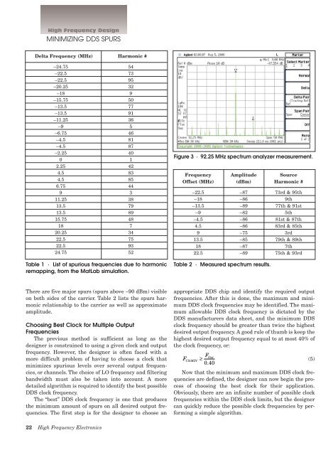
Figure 3 · 92.25 MHz spectrum analyzer measurement.<br />
Frequency Amplitude Source<br />
Offset (MHz) (dBm) Harmonic #<br />
–22.5 –87 73rd & 95th<br />
–18 –86 9th<br />
–13.5 –89 77th & 91st<br />
–9 –82 5th<br />
–4.5 –86 81st & 87th<br />
4.5 –86 83rd & 85th<br />
9 –75 3rd<br />
13.5 –85 79th & 89th<br />
18 –87 7th<br />
22.5 –89 75th & 93rd<br />
Table 2 · Measured spectrum results.<br />
There are five major spurs (spurs above –90 dBm) visible<br />
on both sides <strong>of</strong> the carrier. Table 2 lists the spurs harmonic<br />
relationship to the carrier as well as approximate<br />
amplitude.<br />
Choos<strong>in</strong>g Best Clock for <strong>Multi</strong>ple Output<br />
Frequencies<br />
The previous method is sufficient as long as the<br />
designer is constra<strong>in</strong>ed to us<strong>in</strong>g a given clock and output<br />
frequency. However, the designer is <strong>of</strong>ten faced with a<br />
more difficult problem <strong>of</strong> hav<strong>in</strong>g to choose a clock that<br />
m<strong>in</strong>imizes spurious levels over several output frequencies,<br />
or channels. The choice <strong>of</strong> LO frequency and filter<strong>in</strong>g<br />
bandwidth must also be taken <strong>in</strong>to account. A more<br />
detailed algorithm is required to identify the best possible<br />
<strong>DDS</strong> clock frequency.<br />
The “best” <strong>DDS</strong> clock frequency is one that produces<br />
the m<strong>in</strong>imum amount <strong>of</strong> spurs on all desired output frequencies.<br />
The first step is for the designer to choose an<br />
appropriate <strong>DDS</strong> chip and identify the required output<br />
frequencies. After this is done, the maximum and m<strong>in</strong>imum<br />
<strong>DDS</strong> clock frequencies may be identified. The maximum<br />
allowable <strong>DDS</strong> clock frequency is dictated by the<br />
<strong>DDS</strong> manufacturers data sheet, and the m<strong>in</strong>imum <strong>DDS</strong><br />
clock frequency should be greater than twice the highest<br />
desired output frequency. A good rule <strong>of</strong> thumb is keep the<br />
highest desired output frequency equal to at most 40% <strong>of</strong><br />
the clock frequency, or:<br />
FOut<br />
FClkMIN<br />
≥ (5)<br />
040 .<br />
Now that the m<strong>in</strong>imum and maximum <strong>DDS</strong> clock frequencies<br />
are def<strong>in</strong>ed, the designer can now beg<strong>in</strong> the process<br />
<strong>of</strong> choos<strong>in</strong>g the best clock for their application.<br />
Obviously, there are an <strong>in</strong>f<strong>in</strong>ite number <strong>of</strong> possible clock<br />
frequencies with<strong>in</strong> the <strong>DDS</strong> clock limits, but the designer<br />
can quickly reduce the possible clock frequencies by perform<strong>in</strong>g<br />
a simple algorithm.<br />
22 High Frequency Electronics