Improving the Bandwidth of Simple Matching Networks
Improving the Bandwidth of Simple Matching Networks
Improving the Bandwidth of Simple Matching Networks

You also want an ePaper? Increase the reach of your titles
YUMPU automatically turns print PDFs into web optimized ePapers that Google loves.
High Frequency Design<br />
MATCHING NETWORKS<br />
From March 2008 High Frequency Electronics<br />
Copyright © 2008 Summit Technical Media, LLC<br />
<strong>Improving</strong> <strong>the</strong> <strong>Bandwidth</strong><br />
<strong>of</strong> <strong>Simple</strong> <strong>Matching</strong> <strong>Networks</strong><br />
By Gary Breed<br />
Editorial Director<br />
This tutorial describes<br />
methods for broadbanding<br />
matching networks using<br />
cascaded sections and<br />
compensating reactance<br />
Impedance matching<br />
is probably <strong>the</strong> most<br />
engineering task in<br />
RF/microwave design.<br />
This tutorial is intended<br />
to demonstrate <strong>the</strong> first<br />
steps from simple twoand<br />
three-element networks that are designed<br />
for a specific center frequency, to larger networks<br />
that provide an acceptable match over a<br />
wider bandwidth. These wider bandwidth networks<br />
are important for modern communications<br />
systems that have operating bandwidths<br />
that are much wider than older technologies<br />
using FM and BPSK modulation. Even at narrower<br />
bandwidths, many digital modulation<br />
formats require flat amplitude and linear<br />
phase response, which can be achieved by<br />
using wideband matching networks, which<br />
have much smaller variation over a signal’s<br />
occupied bandwidth.<br />
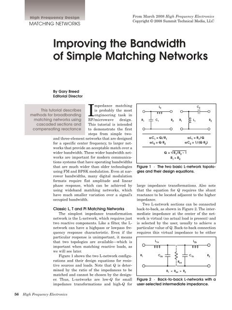
Classic L, T and Pi <strong>Matching</strong> <strong>Networks</strong><br />
The simplest impedance transformation<br />
network is <strong>the</strong> L-network, which requires just<br />
two reactive components. Like a filter, <strong>the</strong> L-<br />
network can have a highpass or lowpass frequency<br />
response characteristic. Even if <strong>the</strong><br />
particular response is unimportant, it means<br />
that two topologies are available—which is<br />
important when matching reactive loads, as<br />
we will see later.<br />
Figure 1 shows <strong>the</strong> two L-network configurations<br />
and <strong>the</strong>ir design equations for resistive<br />
sources and loads. Note that Q is determined<br />
by <strong>the</strong> ratio <strong>of</strong> <strong>the</strong> impedances to be<br />
matched and cannot be chosen by <strong>the</strong> designer.<br />
Thus, L-networks are low-Q for small<br />
impedance transformations and high-Q for<br />
R 1 C 1 R 2 R 1<br />
ω C 1 = Q/R 1<br />
ω L 2 = Q·R 2<br />
Q= √ R 1 /R 2 – 1<br />
ω C 2 = 1/(Q·R 2 )<br />
R 1 > R 2<br />
ω L 1 = R 1 /Q<br />
Figure 1 · The two basic L-network topologies<br />
and <strong>the</strong>ir design equations.<br />
large impedance transformations. Also note<br />
that <strong>the</strong> equation for Q requires <strong>the</strong> shunt<br />
reactance to be located adjacent to <strong>the</strong> higher<br />
impedance.<br />
Two L-network sections can be connected<br />
back-to-back, as shown in Figure 2. The intermediate<br />
impedance at <strong>the</strong> center <strong>of</strong> <strong>the</strong> network<br />
is virtual (no actual load is present) and<br />
is selected by <strong>the</strong> user, usually to achieve a<br />
particular value <strong>of</strong> Q. Back-to-back connection<br />
requires this virtual impedance to be ei<strong>the</strong>r<br />
Figure 2 · Back-to-back L-networks with a<br />
user-selected intermediate impedance.<br />
C 2<br />
L 2<br />
L 1 R 2<br />
L 1a<br />
R 1 C 2a<br />
C 1b<br />
R Int<br />
R 1 < R Int > R 2<br />
L 2b<br />
R 2<br />
56 High Frequency Electronics
High Frequency Design<br />
MATCHING NETWORKS<br />
Figure 3 · T- and Pi-networks combine <strong>the</strong> center components<br />
<strong>of</strong> back-to-back L-networks. Additional topologies<br />
are illustrated in Ref. [1).<br />
higher (as shown in Fig. 2) or lower than both <strong>the</strong> source<br />
and load impedance.<br />
The center components <strong>of</strong> Figure 2 can be combined<br />
into a single component, with <strong>the</strong> result being <strong>the</strong> T-network.<br />
When <strong>the</strong> intermediate impedance is lower than<br />
<strong>the</strong> source and load, <strong>the</strong> result <strong>of</strong> combining <strong>the</strong> center<br />
components is <strong>the</strong> Pi-network. Figure 3 shows some <strong>of</strong> <strong>the</strong><br />
ways that two L-networks can create T- and Pi-networks<br />
[1]. The choice among <strong>the</strong>se topologies is determined by<br />
such factors as DC continuity and highpass, lowpass or<br />
bandpass frequency response. Practical component values<br />
are a major consideration in some cases, especially at<br />
high power levels.<br />
R S = 50Ω<br />
Two L-networks<br />
Two L-networks<br />
L 1a<br />
6.36 nH<br />
C 2a<br />
8.05 pF<br />
R int<br />
Pi-networks<br />
T-networks<br />
L 2b<br />
1.37 nH<br />
C 1b<br />
17.4 pF<br />
f 0 = 850 MHz R int = √ 50 × 5 = 15.81Ω<br />
R L = 5Ω<br />
Figure 4 · Cascaded L-network example, with each<br />
section having a lower Q for improved bandwidth.<br />
Broadbanding with Cascaded L-<strong>Networks</strong><br />
Although T- and Pi-networks represent great flexibility<br />
in design parameter choices, <strong>the</strong>y have narrower frequency<br />
response than a simple L-network. If wider bandwidth<br />
is <strong>the</strong> primary objective, L-networks can be cascaded<br />
in series ra<strong>the</strong>r than back-to-back, such as <strong>the</strong> 850<br />
MHz 5-ohm to 50-ohm network shown in Figure 4 [2].<br />
With cascaded sections, <strong>the</strong> lowest Q (and widest<br />
bandwidth) is achieved when <strong>the</strong> intermediate impedance<br />
is <strong>the</strong> geometric mean <strong>of</strong> <strong>the</strong> source and load impedances.<br />
For example, with source and load impedances <strong>of</strong> 5 and 50<br />
ohms, a single L-network would have a Q <strong>of</strong> 3. When two<br />
sections are cascaded with √(50 × 5), or 15.81 ohms, as <strong>the</strong><br />
intermediate impedance, each section has a Q <strong>of</strong> 1.47.<br />
With ideal, lossless components, <strong>the</strong> lower Q results in<br />
more than 3 times greater bandwidth near <strong>the</strong> center frequency<br />
(between <strong>the</strong> 0.1 dB points) [2].<br />
Figure 5 is a plot <strong>of</strong> <strong>the</strong> impedance at <strong>the</strong> 50-ohm port<br />
for <strong>the</strong> cascaded network <strong>of</strong> Figure 4, compared to a single<br />
lowpass L-network. It is easy to see that <strong>the</strong><br />
impedance deviation <strong>of</strong> <strong>the</strong> cascaded networks is far less<br />
than <strong>the</strong> single L-network section over this 35% bandwidth<br />
range.<br />
Wider bandwidths and flatter impedance curves can<br />
be achieved by cascading more sections with <strong>the</strong> additional<br />
intermediate impedances creating smaller<br />
impedance ratios, and correspondingly lower Q for each<br />
section.<br />
Incorporating Reactances<br />
The above discussion was for resistive loads, but most<br />
practical applications involve loads that include reactance.<br />
The usual design procedure is to cancel <strong>the</strong> load<br />
reactance, <strong>the</strong>n match <strong>the</strong> remaining resistive component<br />
to <strong>the</strong> system impedance. Figure 6 shows <strong>the</strong> two ways<br />
that reactance can be cancelled: (a) an equal but opposite<br />
sign reactance in series, and (b) a parallel reactance that<br />
resonates with <strong>the</strong> load reactance. A 5 –j5 ohm load is<br />
shown in this example.<br />
The manner in which <strong>the</strong> reactance <strong>of</strong> <strong>the</strong> load is<br />
Resistance (ohms) – solid lines<br />
75<br />
70<br />
65<br />
60<br />
55<br />
50<br />
45<br />
40<br />
35<br />
30<br />
25<br />
25<br />
20<br />
15<br />
10<br />
5<br />
0<br />
–5<br />
–10<br />
–15<br />
–20<br />
–25<br />
700 750 800 850 900 950 1000<br />
Frequency (MHz)<br />
Figure 5 · Impedance at <strong>the</strong> 50 ohm port <strong>of</strong> a 5- to 50-<br />
ohm matching network: Example <strong>of</strong> Fig. 4 (red); Single<br />
section lowpass L-network (blue).<br />
Reactance (ohms) – dotted lines<br />
58 High Frequency Electronics
High Frequency Design<br />
MATCHING NETWORKS<br />
70<br />
65<br />
60<br />
55<br />
50<br />
45<br />
40<br />
35<br />
30<br />
25<br />
20<br />
20<br />
15<br />
10<br />
5<br />
0<br />
–5<br />
–10<br />
–15<br />
–20<br />
–25<br />
–30<br />
700 750 800 850 900 950 1000<br />
Frequency (MHz)<br />
R S<br />
50Ω<br />
R S<br />
50Ω<br />
R eff<br />
5 ± j0Ω<br />
(a) Series reactance (cancellation)<br />
R eff<br />
10 ± j0Ω<br />
X L = +j5Ω<br />
X L =<br />
+j10Ω<br />
R L<br />
5 – j5Ω<br />
R L<br />
5 – j5Ω<br />
Resistance (ohms) – solid lines<br />
Reactance (ohms) – dotted lines<br />
(b) Parallel reactance (resonating)<br />
Figure 6 · Two methods for cancelling <strong>the</strong> load reactance,<br />
combined with matching <strong>the</strong> resulting nonreactive<br />
impedance to a 50-ohm system.<br />
incorporated into <strong>the</strong> matching network affects bandwidth.<br />
The finished network can save a component by<br />
combining <strong>the</strong> series cancelling reactance with <strong>the</strong> adjacent<br />
matching component, but <strong>the</strong> resonating solution<br />
has a wider bandwidth.<br />
In Fig. 6(a), note that <strong>the</strong> effective load is 5 ohms for<br />
<strong>the</strong> series cancelling method, but is 10 ohms for <strong>the</strong> resonating<br />
inductor method <strong>of</strong> Fig. 6(b). This reduces <strong>the</strong><br />
magnitude <strong>of</strong> <strong>the</strong> impedance transformation by <strong>the</strong> L-network,<br />
which was previously shown to result in a wider<br />
matching bandwidth. While this circuit has significant<br />
variation in impedance away from <strong>the</strong> center frequency,<br />
this has a much smaller effect on bandwidth than <strong>the</strong><br />
increased effective load impedance.<br />
The results for this example, using a center frequency<br />
<strong>of</strong> 850 MHz, is shown in Figure 7, which is a comparison<br />
<strong>of</strong> <strong>the</strong> impedances at <strong>the</strong> source port for <strong>the</strong> two options <strong>of</strong><br />
Fig. 6. The smaller impedance deviation for <strong>the</strong> resonating<br />
solution <strong>of</strong> Fig. 6(b) is clearly illustrated.<br />
Some Additional Considerations<br />
This tutorial has presented some <strong>of</strong> <strong>the</strong> “first steps” in<br />
<strong>the</strong> path from narrowband to broadband matching. There<br />
are many additional techniques that are involved in fur<strong>the</strong>r<br />
bandwidth improvement, as well as for implementing<br />
matching networks with practical component values.<br />
Below are a few notes on some <strong>of</strong> those techniques, along<br />
with notes on o<strong>the</strong>r issues that arise practical matching<br />
network design.<br />
Transmission line equivalents—All designs using<br />
lumped elements may use transmission line elements, as<br />
well. The choice depends on <strong>the</strong> physical construction<br />
method, frequency <strong>of</strong> operation and, in some cases, is used<br />
Figure 7 · Impedance at R S<br />
port for <strong>the</strong> two matching<br />
options <strong>of</strong> Fig. 6(a) (blue) and Fig. 6(b) (red), implemented<br />
at f 0<br />
= 850 MHz.<br />
to replace components with non-optimum values.<br />
Trading loss for bandwidth—Often, a very low resistance<br />
or high reactance load, such as <strong>the</strong> gate <strong>of</strong> some<br />
power FET devices, can be more easily matched for wide<br />
bandwidth by adding a series resistance to raise <strong>the</strong> effective<br />
impedance. When <strong>the</strong> additional loss can be tolerated,<br />
this technique can greatly simplify broadband matching<br />
network design.<br />
Non-standard impedances—Many matching tasks<br />
involve interfacing between devices or circuits that are<br />
both higher or lower than <strong>the</strong> typical 50-ohm system<br />
impedance. Unless <strong>the</strong>re is a need to test individual modules,<br />
or to separate <strong>the</strong> modules for isolation, matching<br />
<strong>the</strong> actual impedances will result in <strong>the</strong> simplest or easiest<br />
to implement network.<br />
Practical component values—With several options for<br />
matching topologies, <strong>the</strong> choice between <strong>the</strong>m will <strong>of</strong>ten<br />
be based on <strong>the</strong> component values. The considerations<br />
include loss (e.g., large inductors with relatively low Q),<br />
impractical component values, and high currents or voltages<br />
at <strong>the</strong> various points in <strong>the</strong> network.<br />
Reactance <strong>of</strong> <strong>the</strong> load—The magnitude <strong>of</strong> <strong>the</strong> load<br />
reactance and <strong>the</strong> slope <strong>of</strong> reactance change across <strong>the</strong><br />
desired band must be accommodated in any broadband<br />
matching network design. This will affect <strong>the</strong> choice <strong>of</strong><br />
topology and complexity <strong>of</strong> <strong>the</strong> network.<br />
References<br />
1. Chris Bowick, et al, RF Circuit Design, 2nd ed.,<br />
Newnes imprint, Elsevier 2008, Chapter 4.<br />
2. Les Besser, Rowan Gilmore, Practical RF Circuit<br />
Design for Modern Wireless Systems, Artech House 2003,<br />
Chapter 5.<br />
3. Andrei Grebennikov, RF and Microwave Power<br />
Amplifier Design, McGraw-Hill 2005, Chapters 4 and 8.<br />
60 High Frequency Electronics