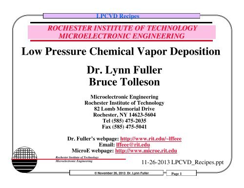
Low Pressure Chemical Vapor Deposition Dr. Lynn Fuller Bruce ...
Low Pressure Chemical Vapor Deposition Dr. Lynn Fuller Bruce ...
Low Pressure Chemical Vapor Deposition Dr. Lynn Fuller Bruce ...

You also want an ePaper? Increase the reach of your titles
YUMPU automatically turns print PDFs into web optimized ePapers that Google loves.
LPCVD Recipes<br />
ROCHESTER INSTITUTE OF TECHNOLOGY<br />
MICROELECTRONIC ENGINEERING<br />
<strong>Low</strong> <strong>Pressure</strong> <strong>Chemical</strong> <strong>Vapor</strong> <strong>Deposition</strong><br />
Rochester Institute of Technology<br />
Microelectronic Engineering<br />
<strong>Dr</strong>. <strong>Lynn</strong> <strong>Fuller</strong><br />
<strong>Bruce</strong> Tolleson<br />
Microelectronic Engineering<br />
Rochester Institute of Technology<br />
82 Lomb Memorial <strong>Dr</strong>ive<br />
Rochester, NY 14623-5604<br />
Tel (585) 475-2035<br />
Fax (585) 475-5041<br />
<strong>Dr</strong>. <strong>Fuller</strong>’s webpage: http://www.rit.edu/~lffeee<br />
Email: lffeee@rit.edu<br />
MicroE webpage: http://www.microe.rit.edu<br />
11-26-2013 LPCVD_Recipes.ppt<br />
© November 26, 2013 <strong>Dr</strong>. <strong>Lynn</strong> <strong>Fuller</strong> Page 1
LPCVD Recipes<br />
OUTLINE<br />
Introduction<br />
LPCVD Nitride<br />
Stociometric<br />
<strong>Low</strong> Stress – Silicon Rich<br />
Stress in Nitride Films<br />
LPCVD Poly<br />
Poly for CMOS (6000Å)<br />
Poly for MEMS (2µm High Dep Rate)<br />
Stress in Poly Films<br />
Doping Poly<br />
LPCVD Oxide (LTO)<br />
Uniformity<br />
LPCVD Parylene<br />
Rochester Institute of Technology<br />
Microelectronic Engineering<br />
© November 26, 2013 <strong>Dr</strong>. <strong>Lynn</strong> <strong>Fuller</strong> Page 2
LPCVD Recipes<br />
LOW PRESSURE CHEMICAL VAPOR DEPOSITION<br />
(LPCVD)<br />
Heat Element<br />
oooooooooooooooooooo<br />
Profile Thermocouple<br />
Clamp<br />
oooooooooooooooooooo<br />
Door<br />
To Pump<br />
and<br />
Burn Box<br />
LPCVD <strong>Low</strong> <strong>Pressure</strong> CVD System<br />
Gas in<br />
Rochester Institute of Technology<br />
Microelectronic Engineering<br />
© November 26, 2013 <strong>Dr</strong>. <strong>Lynn</strong> <strong>Fuller</strong> Page 3
LPCVD Recipes<br />
RIT LPCVD TOOLS<br />
6” LPCVD<br />
4” LPCVD<br />
Top Tube for LTO<br />
Bottom Tube for Poly and Nitride<br />
Rochester Institute of Technology<br />
Microelectronic Engineering<br />
© November 26, 2013 <strong>Dr</strong>. <strong>Lynn</strong> <strong>Fuller</strong> Page 4
LPCVD Recipes<br />
BURN BOX<br />
The correct name is controlled<br />
combustion/reaction system. Exhaust gas<br />
exits through the “burn box” which is<br />
heated to 850 °C. At this temperature the<br />
exhaust gas reacts with air and any<br />
material that can burn is burned under<br />
controlled conditions within the “burn<br />
box”<br />
Rochester Institute of Technology<br />
Microelectronic Engineering<br />
© November 26, 2013 <strong>Dr</strong>. <strong>Lynn</strong> <strong>Fuller</strong> Page 5
LPCVD Recipes<br />
6” LPCVD STOCIOMETRIC NITRIDE<br />
Silicon Nitride (Si3N4) (normal - stociometric):<br />
Temperature = 810 °C Flat from (door to pump)<br />
<strong>Pressure</strong> = 400 mTorr 3SiH2Cl2 + 4NH3 = Si3N4 + 9H2 + 3Cl2<br />
Dichlorosilane (SiH2Cl2) Flow = 60 sccm<br />
Ammonia (NH3) Flow = 150 sccm<br />
Rate = 60 Å/min +/- 10 Å/min<br />
non uniformity of ~ 10%<br />
At 300 mTorr with same conditions as above<br />
Rate = 55 Å/min +/- 10%<br />
non uniformity ~ 3%<br />
Silicon Nitride (Si3N4) (low - stress)<br />
Temperature = 800 °C Flat<br />
<strong>Pressure</strong> =<br />
Dichlorosilane = 200<br />
Ammonia = 20<br />
Rate =<br />
non uniformity =<br />
Tough on pump and burn box, lots of HCL and Cl byproducts<br />
Rochester Institute of Technology<br />
Microelectronic Engineering<br />
© November 26, 2013 <strong>Dr</strong>. <strong>Lynn</strong> <strong>Fuller</strong> Page 6
LPCVD Recipes<br />
4” LPCVD STOCIOMETRIC NITRIDE<br />
Silicon Nitride (Si3N4) (normal - stociometric):<br />
Temperature = 790-800-810 °C Ramp from (door to pump)<br />
<strong>Pressure</strong> = 375 mTorr 3SiH2Cl2 + 4NH3 = Si3N4 + 9H2 + 3Cl2<br />
Dichlorosilane (SiH2Cl2) Flow = 60 sccm<br />
Ammonia (NH3) Flow = 150 sccm<br />
Rate = 60 Å/min +/- 10 Å/min<br />
Rochester Institute of Technology<br />
Microelectronic Engineering<br />
© November 26, 2013 <strong>Dr</strong>. <strong>Lynn</strong> <strong>Fuller</strong> Page 7
LPCVD Recipes<br />
STRESS IN SILICON NITRIDE FILMS<br />
Compressively stressed films would like to expand parallel to the<br />
substrate surface, and in the extreme, films in compressive stress will<br />
buckle up on the substrate. Films in tensile stress, on the other hand,<br />
would like to contract parallel to the substrate, and may crack if their<br />
elastic limits are exceeded. Stresses can be negative or positive or near<br />
zero depending on many parameters.<br />
tensile<br />
negative<br />
positive<br />
compressive<br />
Rochester Institute of Technology<br />
Microelectronic Engineering<br />
© November 26, 2013 <strong>Dr</strong>. <strong>Lynn</strong> <strong>Fuller</strong> Page 8
LPCVD Recipes<br />
STRESS IN NITRIDE FILMS<br />
Stress in an 8000 A<br />
Nitride Film causing<br />
fracture<br />
Rochester Institute of Technology<br />
Microelectronic Engineering<br />
© November 26, 2013 <strong>Dr</strong>. <strong>Lynn</strong> <strong>Fuller</strong> Page 9
LPCVD Recipes<br />
LOW STRESS SILICON RICH Si3N4<br />
ADE Measured stress for various Ammonia:Dichlorosilane Flow<br />
Ratios<br />
Flow Stress x E 9 dynes/cm2<br />
10:1 +14.63<br />
5:1 +14.81<br />
2.5:1 +12.47 * Stress; σ = (E/(6(1-v)))*(D 2 /(rt))<br />
1:1 +10.13 where E is Youngs modulus,<br />
1:2.5 +7.79 v is Poissons ratio,<br />
1:5 +3 D and t are substrate and film thickness<br />
1:10 0 r is radius of curvature (+ for tensile)<br />
* standard recipe<br />
T.H Wu, “Stress in PSG and Nitride Films as Related to Film<br />
Properties and Annealing”, Solid State Technology, p 65-71,May ‘92<br />
Rochester Institute of Technology<br />
Microelectronic Engineering<br />
10 dyne/cm 2 = 1 newton/m 2 = 1 Pascal<br />
© November 26, 2013 <strong>Dr</strong>. <strong>Lynn</strong> <strong>Fuller</strong> Page 10
LPCVD Recipes<br />
MEASUREMENT OF STRESS IN Si3N4<br />
Kenneth L. Way, Jr. did his senior project on stress in silicon nitride<br />
films as a function of the ratio of ammonia to dichlorosilane.<br />
Samples were coated with various flows and stress was measured at<br />
ADE corporation. The silicon nitride was etched off of the backside<br />
of the wafer so that the stress curvature was due to the layer on the<br />
front side only. <strong>Dr</strong>. Lane said the nitride runs at 1:10<br />
(ammonia:dichlorosilane) ratios are rough on the pumping system.<br />
Compressive Stress<br />
Tensile Stress<br />
<strong>Dr</strong>. Grande sent samples to Kodak for stress measurement. He<br />
found stress of +900 MPa Tensile for the standard Nitride recipe for<br />
1500 A thickness, 1-29-2000<br />
Rochester Institute of Technology<br />
Microelectronic Engineering<br />
10 dyne/cm 2 = 1 newton/m 2 = 1 Pascal<br />
© November 26, 2013 <strong>Dr</strong>. <strong>Lynn</strong> <strong>Fuller</strong> Page 11
LPCVD Recipes<br />
6” LPCVD LOW STRESS SILICON NITRIDE<br />
Silicon Nitride (Si3N4) (low - stress)<br />
Temperature = 800 °C Flat<br />
<strong>Pressure</strong> =<br />
Dichlorosilane = 200<br />
Ammonia = 20<br />
Rate =<br />
non uniformity =<br />
Tough on pump and burn box, lots of HCL and Cl byproducts, we do not<br />
run this process very often.<br />
Rochester Institute of Technology<br />
Microelectronic Engineering<br />
© November 26, 2013 <strong>Dr</strong>. <strong>Lynn</strong> <strong>Fuller</strong> Page 12
LPCVD Recipes<br />
4” LPCVD LOW STRESS SILICON NITRIDE<br />
Silicon Nitride (Si3N4) (low stress – silicon rich):<br />
Temperature = 790-800-810 °C Ramp from (door to pump)<br />
<strong>Pressure</strong> = 650 mTorr 3SiH2Cl2 + 4NH3 = Si3N4 + 9H2 + 3Cl2<br />
Dichlorosilane (SiH2Cl2) Flow = 200 sccm<br />
Ammonia (NH3) Flow = 20 sccm<br />
Rate = 80 Å/min +/- 10 Å/min<br />
Films can be deposited up to about 5000 Å directly on silicon before the stress<br />
is so large that the film fractures (<strong>Dr</strong>. Lane, <strong>Dr</strong>. <strong>Fuller</strong>). Pad oxide under the<br />
nitride film and special silicon rich nitride films may allow nitride film<br />
thickness over 5000 Å.<br />
9-6-96 <strong>Dr</strong>. <strong>Fuller</strong> did a 100 min deposition giving 8100Å (center) to 8800Å<br />
(edge) nitride thickness which did not fracture due to stress. It is a definite<br />
improvement.<br />
Rochester Institute of Technology<br />
Microelectronic Engineering<br />
© November 26, 2013 <strong>Dr</strong>. <strong>Lynn</strong> <strong>Fuller</strong> Page 13
LPCVD Recipes<br />
6” LPCVD POLYSILICON FOR CMOS<br />
Polysilicon <strong>Deposition</strong>:<br />
Temperature = 610 °C<br />
<strong>Pressure</strong> = 300 mTorr<br />
Gas = Silane (SiH4)<br />
Flow = 90 sccm<br />
Rate = 64 Å/min<br />
SiH4 = Si + 2H2<br />
Rochester Institute of Technology<br />
Microelectronic Engineering<br />
© November 26, 2013 <strong>Dr</strong>. <strong>Lynn</strong> <strong>Fuller</strong> Page 14
LPCVD Recipes<br />
6” LPCVD POLYSILICON FOR MEMS<br />
High Dep. Rate Polysilicon <strong>Deposition</strong>:<br />
Temperature = 650 °C SiH4 = Si + 2H2<br />
<strong>Pressure</strong> = 300 mTorr<br />
Gas = Silane (SiH4)<br />
Flow = 400 sccm<br />
Rate = 200 Å/min (~ 3 times the normal dep. rate at 610 °C)<br />
Thicker films have larger grain size (grain size ~ equal to film thickness) and<br />
thus a rougher appearance.<br />
Rochester Institute of Technology<br />
Microelectronic Engineering<br />
© November 26, 2013 <strong>Dr</strong>. <strong>Lynn</strong> <strong>Fuller</strong> Page 15
LPCVD Recipes<br />
4” LPCVD POLYSILICON FOR CMOS<br />
Polysilicon <strong>Deposition</strong>:<br />
Temperature = 610 °C<br />
<strong>Pressure</strong> = 300 mTorr<br />
Gas = Silane (SiH4)<br />
Flow = 90 sccm<br />
Rate = 77 Å/min<br />
SiH4 = Si + 2H2<br />
Fronts<br />
device wafers<br />
every other slot<br />
Rochester Institute of Technology<br />
Microelectronic Engineering<br />
5 fillers every<br />
other slot<br />
1 filler<br />
at end<br />
© November 26, 2013 <strong>Dr</strong>. <strong>Lynn</strong> <strong>Fuller</strong> Page 16
LPCVD Recipes<br />
4” LPCVD POLYSILICON FOR MEMS<br />
High Dep. Rate Polysilicon <strong>Deposition</strong>:<br />
Temperature = 650 °C SiH4 = Si + 2H2<br />
<strong>Pressure</strong> = 300 mTorr<br />
Gas = Silane (SiH4)<br />
Flow = 90 sccm<br />
Rate = 235 Å/min (~ 3 times the normal dep. rate at 610 °C)<br />
Thicker films have larger grain size (grain size ~ equal to film thickness) and<br />
thus a rougher appearance.<br />
Rochester Institute of Technology<br />
Microelectronic Engineering<br />
© November 26, 2013 <strong>Dr</strong>. <strong>Lynn</strong> <strong>Fuller</strong> Page 17
LPCVD Recipes<br />
DOPING POLYSILICON FROM SPIN-ON DOPANTS<br />
When using poly as a conductor in integrated circuits it is desirable to have low resistivity.<br />
Doping at 1000 °C for 20 min using Emulsitone Co., 19 Leslie Court, Whippany, NJ 07981<br />
Tel (201)386-0053; Emitter Diffusion Source N250 spin-on dopant gives 10-15 ohm/sq sheet<br />
resistance for 0.75 um thick poly. (The Allied Signal Inc., 1090 South Milpitas Boulevard,<br />
Milpitas, CA 95035, Tel (408)946-2411, Accuspin P-854 dopant gives higher resistivity in<br />
the range of 100 ohm/sq.)<br />
There is no problem unless one is concerned with the possibility of the dopant going through<br />
a thin gate oxide and affecting the underlying substrate. In this case the doping needs to be<br />
adequate however the subsequent high temperature steps each drive the dopant further<br />
through the gate oxide. CV measurements can be used to see if the dopant gets through to<br />
the substrate. For n-type dopant and p-type substrate one would expect a shift to the left if<br />
the dopant goes through the gate. We found that doping at 1000 C for 10 min soak, using<br />
N250 spin on source, followed by 60 min in nitrogen at 1000 C did not cause a shift to the<br />
left in the CV plot. (actually shifted right .... similar to anneal or sinter) We did not test the<br />
breakdown voltage or effect of gate oxide doping on breakdown voltage. We did not try<br />
additional time at 1000 C in Nitrogen looking for shift to left in CV plot.<br />
Rochester Institute of Technology<br />
Microelectronic Engineering<br />
© November 26, 2013 <strong>Dr</strong>. <strong>Lynn</strong> <strong>Fuller</strong> Page 18
LPCVD Recipes<br />
DOPING POLYSILICON BY ION IMPLANT<br />
In the advanced CMOS process we want N+ poly on the NMOSFET<br />
and P+ poly on the PMOSFET. So the poly is deposited undoped and<br />
during D/S implant the poly is also doped.<br />
In the submicron CMOS process we dope the poly after deposition n+<br />
for both transistors. We use a dose of 2E16 which is the highest dose<br />
that we typically do at RIT. Since there is no resist on the wafer we do<br />
not have to consider heating effects during implant. The current is set<br />
as high as possible, often 500uA or more.<br />
Rochester Institute of Technology<br />
Microelectronic Engineering<br />
© November 26, 2013 <strong>Dr</strong>. <strong>Lynn</strong> <strong>Fuller</strong> Page 19
LPCVD Recipes<br />
DOPING POLYSILICON BY ION IMPLANT<br />
In some analog CMOS processes we want high sheet resistance poly<br />
resistors for voltage dividers, etc. The measured resistor data below<br />
shows sheet resistance versus Boron (B11) dose for a 3500Å poly layer<br />
after 30 min.1000 °C anneal.<br />
R=1/slope; Rhos=R / #sqs; Rho=Rhos x thickness (3500Å); Dose=implanter setting<br />
R wafer 4 = 106 G ; Rhos = 2.94 Gohm/sq; Rho = 103K ohm-cm; Dose=1E12 cm-2<br />
R wafer 3 = 339 G ; Rhos = 9.42 Gohm/sq; Rho = 330K ohm-cm; Dose = 3E11<br />
R wafer 2 = 943 G ; Rhos = 26.2 Gohm/sq; Rho = 917K ohm-cm; Dose = 6E11<br />
R wafer 1 = 1104 G; Rhos = 30.7 Gohm/sq; Rho = 1075K ohm-cm; Dose = 1E11<br />
Rochester Institute of Technology<br />
Microelectronic Engineering<br />
© November 26, 2013 <strong>Dr</strong>. <strong>Lynn</strong> <strong>Fuller</strong> Page 20
LPCVD Recipes<br />
STRESS IN POLY FILMS<br />
Stress in poly films can cause<br />
buckling and bending of beams<br />
and cantilever structures. When<br />
doping poly after deposition the<br />
high temperatures (1000 C) will<br />
anneal stress. Undoped poly<br />
structures require an anneal.<br />
Rochester Institute of Technology<br />
Microelectronic Engineering<br />
© November 26, 2013 <strong>Dr</strong>. <strong>Lynn</strong> <strong>Fuller</strong> Page 21
LPCVD Recipes<br />
LOW TEMPERATURE OXIDE (LTO)<br />
Wafers are loaded back<br />
to back in caged boat.<br />
The boat is filled with<br />
dummy wafer to total<br />
25 wafers. Monitor<br />
wafer is placed in the<br />
middle. Injector tubes<br />
direct the gas (SiH4 and<br />
O2) directly under the<br />
middle of the caged<br />
boat.<br />
Rochester Institute of Technology<br />
Microelectronic Engineering<br />
Caged Boat<br />
© November 26, 2013 <strong>Dr</strong>. <strong>Lynn</strong> <strong>Fuller</strong> Page 22
LPCVD Recipes<br />
IMPROVED UNIFORMITY OF LTO WITH CAGED BOAT<br />
In 4” LPCVD<br />
Rochester Institute of Technology<br />
Microelectronic Engineering<br />
Using 6” LPCVD<br />
Caged Boat and Injectors<br />
© November 26, 2013 <strong>Dr</strong>. <strong>Lynn</strong> <strong>Fuller</strong> Page 23
LPCVD Recipes<br />
6” LTO RECIPE<br />
<strong>Low</strong> Temperature Silicon Oxide:<br />
Temperature = 400 °C SiH4 + O2 = SiO2 + 2H2<br />
<strong>Pressure</strong> = 250 mTorr<br />
Silane (SiH4)<br />
Flow = 40 sccm<br />
Oxygen (O2)<br />
Flow 48 sccm<br />
Rate = 70 Å/min +/- 10 Å/min<br />
7-26-00 LTO @425 °C gave deposition rate of 113 Å/min<br />
Rochester Institute of Technology<br />
Microelectronic Engineering<br />
© November 26, 2013 <strong>Dr</strong>. <strong>Lynn</strong> <strong>Fuller</strong> Page 24
LPCVD Recipes<br />
OXIDE THICKNESS COLOR CHART<br />
Thickness Color Thickness Color<br />
500 Tan 4900 Blue<br />
700 Brown 5000 Blue Green<br />
Blue<br />
1000 Dark Violet - Red Violet 5200 Green<br />
1200 Royal Blue 5400 Yellow Green<br />
Blue<br />
1500 Light Blue - Metallic Blue 5600 GreenYellow<br />
1700 Metallic - very light Yellow Green 5700 Yellow -"Yellowish"(at times appears to be Lt gray or matellic)<br />
2000 LIght Gold or Yellow - Slightly Metallic 5800 Light Orange or Yellow - Pink<br />
2200 Gold with slight Yellow Orange 6000 Carnation Pink<br />
2500 Orange - Melon 6300 Violet Red<br />
2700 Red Violet 6800 "Bluish"(appears Blue violet red, Blue Green, looks grayish) Blue<br />
3000 Blue - Violet Blue 7200 Blue Green - Green<br />
3100 Blue Blue<br />
7700 "Yellowish"<br />
3200 Blue - Blue Green 8000 Orange<br />
3400 Light Green 8200 Salmon<br />
3500 Green - Yellow Green 8500 Dull, LIght Red Violet<br />
3600 Yellow Green 8600 Violet<br />
3700 Yellow 8700 Blue Violet<br />
3900 Light Orange 8900 Blue<br />
Blue<br />
4100 Carnation Pink 9200 Blue Green<br />
4200 Violet Red 9500 Dull Yellow Green<br />
4400 Red Violet 9700 Yellow - "Yellowish"<br />
4600 Violet 9900 Orange<br />
4700 Blue Violet 10000 Carnation Pink<br />
Nitride Thickness = (Oxide Thickness)(Oxide Index/Nitride Index)<br />
Eg. Yellow Nitride Thickness = (2000)(1.46/2.00) = 1460<br />
Rochester Institute of Technology<br />
Microelectronic Engineering<br />
PLAY<br />
© November 26, 2013 <strong>Dr</strong>. <strong>Lynn</strong> <strong>Fuller</strong> Page 25
LPCVD Recipes<br />
NITRIDE MEASUREMENTS<br />
Ellipsometer Program 7 does nitride on pad oxide<br />
Nanospec Program 6 does nitride on pad oxide<br />
Spectromap does nitride on pad oxide<br />
You need to know the value of the pad oxide thickness.<br />
Rochester Institute of Technology<br />
Microelectronic Engineering<br />
© November 26, 2013 <strong>Dr</strong>. <strong>Lynn</strong> <strong>Fuller</strong> Page 26
LPCVD Recipes<br />
PARYLENE DEPOSITION SYSTEM<br />
Approximately 1 gm of<br />
Parylene C gives ~3000Å film<br />
thickness, Deposit 5 wafers per<br />
run.<br />
Descovered we need A174<br />
Adhesion Promotor. <strong>Chemical</strong><br />
name gammamethacryloxypropyltrimethoxy<br />
silane. Spin coat straight from<br />
package at 2000 rpm. Bake on<br />
hot plate at 115 C for 1 min.<br />
Rochester Institute of Technology<br />
See: http://www.scscookson.com/parylene/properties.cfm<br />
Microelectronic Engineering<br />
© November 26, 2013 <strong>Dr</strong>. <strong>Lynn</strong> <strong>Fuller</strong> Page 27
LPCVD Recipes<br />
PARYENE MINI OPERATION MANUAL<br />
Mini Operation Manual for the PDS-2010 – Parylene <strong>Deposition</strong> System<br />
Revision 4-30-04<br />
<strong>Dr</strong>. <strong>Lynn</strong> <strong>Fuller</strong>, Germain Fenger<br />
Clean up Prior to <strong>Deposition</strong>:<br />
1. Open the storage drawer under the white table. Contains Parylene powder,<br />
cleaning tools, microclean-90 spray cleaner, concentrate of microclean-90 and<br />
spare parts. (If necessary mix more microclean-90 by diluting with water a few<br />
caps full per spray bottle)<br />
2. Clean around seal, on Bell Jar and Stage. Only clean the inside of Bell Jar and<br />
center on stage if there is visible pealing.<br />
3. Spray microclean-90 on parts that have been cleaned and are exposed.<br />
4. Verify that the small pressure sensor hole is clear of deposition, if it is not use a<br />
small hook tool to remove the deposition. Do not push the parylene residue further<br />
in the hole.<br />
5. Clean the chiller (back right corner). Remove the chiller being careful of the tubes<br />
on the end of the chiller (inside of black cover) for they bend easily. Use a scour<br />
pad to remove the majority of the deposition, some deposition may require the use<br />
of a razor blade. Spray with micro-90 when done.<br />
6. Remove <strong>Deposition</strong> Tube and verify that it is not clogged, or the hole that it goes<br />
into.<br />
Set up for <strong>Deposition</strong>:<br />
1. Open the front cabinet door. Unclamp and open the vaporizer door on the lower<br />
left. Remove the aluminum foil Dimer boat. If you need to make a new Dimer<br />
boat see page 18 of the manual.<br />
2. One gram of Parylene type C from Specialty Coating Systems, 5707 West<br />
Minnesota St., Indianapolis, IN 46241, gives1 micrometer of thickness. Measure<br />
out the desired amount of Parylene powder. Use the gram scale near the 4 pt<br />
probe. Lift off the glass cover, turn ON, set zero >0 , set foil on top of scale, set<br />
tear T< (reading should go to zero), using the scoop put some powder on the foil<br />
to desired amount. Pour the measured amount of powder into the aluminum foil<br />
Dimer boat.<br />
3. Place boat with powder in the vaporizer and close and clamp the door.<br />
4. Place wafers in the designated boats (in storage cabinet).<br />
Rochester Institute of Technology<br />
Microelectronic Engineering<br />
Start System:<br />
1. Card Swipe in.<br />
2. Place wafers on stage, pull EMO, turn the switch labeled vaporizer on and verify<br />
that the boat does not rub on anything, if it is found to be rubbing adjust boat<br />
position, turn off vaporizer.<br />
3. Place bell jar on stage.<br />
4. Turn on vaporizer, and again verify that the boat is not rubbing, if it is rubbing<br />
remove bell jar and adjust.<br />
5. While holding the chiller in place, turn right switch to vacuum, once under vacuum<br />
you may release the chiller.<br />
6. Turn on the chiller, (left green switch)<br />
7. Turn on furnace switch and vaporizer.<br />
8. Once pressure reads below 30mTorr (base pressure) push the green button (right).<br />
© November 26, 2013 <strong>Dr</strong>. <strong>Lynn</strong> <strong>Fuller</strong> Page 28
LPCVD Recipes<br />
REFERENCES<br />
1. Silicon Processing for the VLSI Era, Volume 1, 2 nd Edition,<br />
Stanley Wolf, Richard Tauber, Lattice Press, 2000.<br />
2. The Science and Engineering of Microelectronic Fabrication,<br />
Stephen A. Campbell, Oxford University Press, 1996.<br />
Rochester Institute of Technology<br />
Microelectronic Engineering<br />
© November 26, 2013 <strong>Dr</strong>. <strong>Lynn</strong> <strong>Fuller</strong> Page 29