Transistors to Transformations - Intel
Transistors to Transformations - Intel
Transistors to Transformations - Intel

Create successful ePaper yourself
Turn your PDF publications into a flip-book with our unique Google optimized e-Paper software.
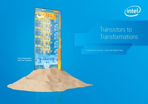
<strong>Transis<strong>to</strong>rs</strong> <strong>to</strong><br />
<strong>Transformations</strong><br />
From Sand <strong>to</strong> Circuits — How <strong>Intel</strong> Makes Chips<br />
22nm 3rd generation<br />
<strong>Intel</strong>® Core processor
“ For years we have see<br />
transis<strong>to</strong>rs can get. Th<br />
structure is a truly rev<br />
and one that should all<br />
the his<strong>to</strong>ric pace of inn<br />
-Gordon E. Moore, Co-founder, <strong>Intel</strong> Corporation, commenting on <strong>Intel</strong>’s radical reinvention of the transis<strong>to</strong>r — the creation of the 22nm 3-D Tri-Gate transis<strong>to</strong>r
n limits <strong>to</strong> how small<br />
is change in the basic<br />
olutionary approach,<br />
ow Moore’s Law and<br />
ovation <strong>to</strong> continue.”
A Smart World<br />
REVOLUTIONARY<br />
For decades, <strong>Intel</strong>’s research and development,<br />
advanced silicon chips, and manufacturing<br />
have brought <strong>to</strong>gether the best of computing,<br />
communications, and consumer electronics <strong>to</strong><br />
enable valuable benefits from technology.<br />
<strong>Intel</strong> continues <strong>to</strong> introduce new process<br />
technologies that deliver more energy-efficient,<br />
secure, and higher-performance products, which<br />
are then designed in<strong>to</strong> your increasingly connected,<br />
smarter devices.<br />
MOORE’S LAW<br />
According <strong>to</strong> Moore’s Law, the number of<br />
transis<strong>to</strong>rs on a chip roughly doubles every<br />
couple of years. As a result, the transis<strong>to</strong>r scale<br />
gets smaller and smaller. As the transis<strong>to</strong>r count<br />
climbs, so does the ability <strong>to</strong> integrate more<br />
capabilities on<strong>to</strong> a chip and increase device<br />
complexity.<br />
The cumulative impact of these spiraling increases<br />
in capabilities enables <strong>to</strong>day’s mobile devices, fuels<br />
the increasingly Internet-connected and<br />
information-rich digital experiences we seek,<br />
and powers industries and our global economy.<br />
Delivering Moore’s Law requires numerous<br />
innovations. <strong>Intel</strong>’s world-first, advanced transis<strong>to</strong>r<br />
design introductions include strained silicon (2003),<br />
45nm with high-k/metal gate silicon technology<br />
(2007), followed by the 32nm 2nd generation<br />
high-k/metal gate silicon technology (2009).<br />
Recently, <strong>Intel</strong> introduced another radical design<br />
change—22nm 3-D Tri-Gate transis<strong>to</strong>rs (2011),<br />
which entered high-volume production in 2012.<br />
YOUR WORLD CONNECTED<br />
“Our vision is very simple: if it consumes electricity,<br />
it’s going <strong>to</strong> end up computing, and if it’s computing,<br />
it will be connected <strong>to</strong> the Internet,” stated Kirk B.<br />
Skaugen, <strong>Intel</strong> Vice President and General Manager<br />
of the PC Client Group. He was describing server<br />
cloud computing capabilities and connected device<br />
growth expected within the next decade at the<br />
Web 2.0 Summit in November 2011.<br />
Forecasts call for 15 billion connected devices 1 and<br />
over three billion connected users 2 by 2015. The<br />
growth of global data through 2015 is expected <strong>to</strong><br />
surpass 4.8 zettabytes per year. 3 At these levels,<br />
each connected user will generate more than four<br />
GB of data traffic every day. That’s the equivalent<br />
of a 4-hour HD movie.<br />
THE POWER TO TRANSFORM<br />
From Ultrabook devices, data centers, and high<br />
performance computing, <strong>to</strong> applications, security,<br />
and <strong>Intel</strong>-powered smartphones and tablets, the<br />
only thing more amazing than <strong>Intel</strong>’s technology is<br />
what you do with it.<br />
Find definitions of italicized words in the “Terminology”<br />
section at the end of this brochure.
2008 *<br />
<strong>Intel</strong>® Core2 Duo processor die<br />
(45nm high-k/metal gate silicon technology)<br />
2010 *<br />
2nd generation <strong>Intel</strong>® Core processor die<br />
(32nm process technology)<br />
2012 *<br />
3rd generation <strong>Intel</strong>® Core processor die<br />
(manufactured on industry-leading 22nm process<br />
technology with 3-D Tri-Gate transis<strong>to</strong>rs)<br />
Die not shown <strong>to</strong> scale.<br />
*Date of high volume production
ADVANCED DESIGN<br />
<strong>Intel</strong> creates industry-leading and world-first<br />
silicon products that introduce more capabilities,<br />
are smaller, more powerful, and use less energy.<br />
While advancing technology, <strong>Intel</strong> incorporates<br />
environmental principles in<strong>to</strong> each step of the<br />
product life cycle. And by anticipating the needs for<br />
the next generation, <strong>Intel</strong>’s success at advanced<br />
chip design has helped drive other innovations in<br />
almost all industries.<br />
WHAT IS A CHIP?<br />
A chip, also known as a die or processor, is a<br />
microelectronic device that can process information<br />
in the form of electrical current traveling along a<br />
circuit. Although they look flat, <strong>to</strong>day’s chips may<br />
have more than 30 layers of complex circuitry<br />
compared <strong>to</strong> five layers on the 4004, <strong>Intel</strong>’s first<br />
processor, introduced in 1971.<br />
HOW CHIPS WORK<br />
The way a chip works is a result of how a chip’s<br />
transis<strong>to</strong>rs and gates are designed and the<br />
use of the chip. A chip can contain millions or<br />
billions of transis<strong>to</strong>rs interconnected in a certain<br />
manner. These transis<strong>to</strong>rs act as switches, either<br />
preventing or allowing electrical current <strong>to</strong> pass<br />
through. A gate turns the transis<strong>to</strong>rs on and off,<br />
allowing electrical currents <strong>to</strong> send, receive, and<br />
process digital data (1s and 0s) as instructions and<br />
information. Chips <strong>to</strong>day can have multiple cores.<br />
THE ULTIMATE PUZZLE<br />
How would you organize something with<br />
1,000,000,000 pieces, and then create a plan<br />
so it can be put <strong>to</strong>gether correctly and on time?<br />
Worldwide teamwork is critical. Precision counts.<br />
Rules matter. Many types of engineers work closely<br />
<strong>to</strong>gether <strong>to</strong> design chips and translate circuit<br />
schematics in<strong>to</strong> mask layers for manufacturing.<br />
Before <strong>Intel</strong> makes chips, engineers ensure the<br />
accuracy of the specification. They begin with a<br />
design or blueprint and consider many fac<strong>to</strong>rs:<br />
What type of chip is needed and why? How many<br />
transis<strong>to</strong>rs can be built on the chip? What is the<br />
optimal chip size? What technology will be available<br />
<strong>to</strong> create the chip? When does the chip need <strong>to</strong><br />
be ready? Where will it be manufactured and<br />
tested? To answer these questions, <strong>Intel</strong> teams<br />
work with cus<strong>to</strong>mers, software companies, and<br />
<strong>Intel</strong>’s marketing, manufacturing, and testing staff.<br />
The design teams take this input and begin the<br />
monumental task of defining a chip’s features<br />
and design.<br />
When the specifications for the chip are ready, <strong>Intel</strong><br />
creates a logic design, an abstract representation<br />
of the hundreds of millions of transis<strong>to</strong>rs and<br />
interconnections that control the flow of electricity<br />
through a chip. After this phase is complete,<br />
designers prepare physical representations of<br />
each layer of the chip and its transis<strong>to</strong>rs. They<br />
then develop stencil-like patterns, or masks, for<br />
each layer of the chip that are used with ultraviolet<br />
(UV) light during a fabrication process called<br />
pho<strong>to</strong>lithography.<br />
To complete the design, testing, and simulation of<br />
a chip, <strong>Intel</strong> uses computer-aided design (CAD)<br />
<strong>to</strong>ols. CAD helps designers create very complex<br />
designs that meet functional, performance, and<br />
power goals. After extensive modeling, simulation,<br />
and verification, the chip is ready for fabrication.<br />
It can take hundreds of engineers working multiple<br />
years <strong>to</strong> design, test, and ready a new chip design<br />
for fabrication.
INTEL ENVIRONMENTAL,<br />
HEALTH, & SAFETY<br />
PRODUCT LIFE CYCLE<br />
From initial research <strong>to</strong> the end of a product’s life,<br />
<strong>Intel</strong> integrates environmental principles and<br />
health and safety practices in<strong>to</strong> each stage.<br />
03<br />
CHEMICAL USE<br />
APPROVAL<br />
Toxicity screening<br />
Hazard classification<br />
Risk evaluation<br />
Substitution alternatives<br />
Control mechanism<br />
Personal protective equipment<br />
02<br />
MATERIALS &<br />
EQUIPMENT SELECTION<br />
Process equipment safety<br />
Restriction of Hazardous<br />
Substances (RoHS) compliance<br />
Electronic Industry<br />
Citizenship Coalition<br />
Material screening <strong>to</strong>ol<br />
Product specs<br />
01<br />
RESEARCH &<br />
DEVELOPMENT<br />
Benign semiconduc<strong>to</strong>r materials<br />
Design for the Environment Principles<br />
Nanotech research<br />
04<br />
INTEL<br />
OPERATIONS<br />
Resource conservation<br />
International Organization for<br />
Standardization (ISO) 14001<br />
Climate-change footprint<br />
Employee safety and wellness<br />
Waste reduction and recycling<br />
05<br />
INTEL<br />
PRODUCTS<br />
Energy efficiency<br />
RoHS compliance<br />
Product packaging reduction<br />
Energy Star*<br />
Halogen-free 4<br />
Lead-free 5<br />
Power-supply energy specifications<br />
Power management software<br />
06<br />
END OF LIFE<br />
Community recycling events<br />
Environmental Protection<br />
Agency (EPA) Plug-In <strong>to</strong> eCycling<br />
Electronic Product Environmental<br />
Assessment Tool (EPEAT)<br />
Environmental education<br />
Waste Electrical and Electronic<br />
Equipment (WEEE) Directive
Global. Connected.<br />
Mission Critical.<br />
<strong>Intel</strong>’s manufacturing leadership includes a global network of high-volume,<br />
technically advanced wafer fabrication facilities, or fabs, that run 24 hours<br />
a day, 7 days a week, 365 days a year.<br />
FABRICATION<br />
The process of making chips is called fabrication.<br />
Inside <strong>Intel</strong>’s ultra-clean fabs, the world’s most<br />
complex, tiniest machines — processors and other<br />
silicon chips — are built in a sustainable manner.<br />
<strong>Intel</strong> fabs are among the most technically advanced<br />
manufacturing facilities in the world. Within these<br />
sophisticated fabs, <strong>Intel</strong> makes chips in a special<br />
area called a cleanroom.<br />
Because particles of dust can ruin the complex<br />
circuitry on a chip, cleanroom air must be ultraclean.<br />
Purified air is constantly recirculated,<br />
entering through the ceiling and exiting through<br />
floor tiles. Technicians put on a special suit,<br />
commonly called a bunny suit, before they enter a<br />
cleanroom. This helps keep contaminants such as<br />
lint and hair off the wafers.<br />
In a cleanroom, a cubic foot of air contains less than<br />
one particle measuring about 0.5 micron (millionth<br />
of a meter) across. That’s thousands of times<br />
cleaner than a hospital operating room.<br />
Au<strong>to</strong>mation has a critical role in a fab. Batches of<br />
wafers are kept clean and are processed quickly<br />
and efficiently by traveling through the fab inside<br />
front-opening unified pods (FOUPs) on an<br />
overhead monorail. Each FOUP receives a barcode<br />
tag that identifies the recipe that will be used <strong>to</strong><br />
make the chips inside. This labeling ensures the<br />
correct processing at each step of fabrication. Each<br />
FOUP contains up <strong>to</strong> 25 wafers and weighs more<br />
than 25 pounds. Production au<strong>to</strong>mation machinery<br />
allows for this FOUP weight, which is <strong>to</strong>o heavy <strong>to</strong><br />
be handled manually by technicians.<br />
Above: 3rd generation <strong>Intel</strong>® Core wafer
Top left: Orange FOUPs carry 300mm wafers in an au<strong>to</strong>mated fab.<br />
Top right: Highly-trained technicians moni<strong>to</strong>r each phase of chip fabrication.<br />
Bot<strong>to</strong>m left: Purified air enters from the ceiling and exits through perforated floor tiles.<br />
Bot<strong>to</strong>m right: The 32nm planar transis<strong>to</strong>r (on left) illustrates current (represented by yellow dots)<br />
flowing in a flat plane under the gate, while <strong>Intel</strong>’s smaller 22nm 3-D Tri-Gate transis<strong>to</strong>r (on right)<br />
illustrates increased current flow over three sides of a vertical fin.
How <strong>Intel</strong> Makes Chips<br />
SAND TO INGOT<br />
Sand<br />
Sand has a high percentage of silicon—the<br />
starting material for computer chips. Silicon is a<br />
semiconduc<strong>to</strong>r, meaning that it can be turned in<strong>to</strong><br />
an excellent conduc<strong>to</strong>r or insula<strong>to</strong>r of electricity<br />
with minor amounts of impurities added.<br />
Melted Silicon<br />
Silicon is purified <strong>to</strong> less than one alien a<strong>to</strong>m per<br />
billion. It is melted and cooled in<strong>to</strong> a solid crystal<br />
lattice cylinder, called an ingot.<br />
Monocrystalline Silicon Ingot<br />
The silicon ingot has a diameter of 300 millimeters<br />
(mm) and weighs about 100 kilograms (kg).<br />
INGOT TO WAFER<br />
Slicing Ingots<br />
The ingot is cut in<strong>to</strong> individual silicon discs called<br />
wafers. Each wafer is about one mm thick.<br />
Polishing Wafers<br />
The wafers are polished <strong>to</strong> a flawless,<br />
mirror-smooth surface. <strong>Intel</strong> buys these<br />
manufacturing-ready wafers.<br />
PHOTOLITHOGRAPHY<br />
Applying Pho<strong>to</strong>resist<br />
Pho<strong>to</strong>lithography is a process that imprints a<br />
specific pattern on the wafer. It starts by applying<br />
a light-sensitive, etch-resistant material called<br />
pho<strong>to</strong>resist on<strong>to</strong> the wafer surface.<br />
Exposing Pho<strong>to</strong>resist<br />
The pho<strong>to</strong>resist is hardened and parts of it are<br />
exposed <strong>to</strong> ultraviolet light, making it soluble. The<br />
light passes through a mask (similar <strong>to</strong> a stencil),<br />
and then through a lens <strong>to</strong> shrink and print circuit<br />
patterns on each layer of every chip on the wafer.<br />
Developing Resist<br />
A chemical process removes the soluble<br />
pho<strong>to</strong>resist, leaving a patterned pho<strong>to</strong>resist<br />
image as determined by what was on the mask.
CHIPS ARE THREE-DIMENSIONAL STRUCTURES<br />
built simultaneously on batches of wafers in a<br />
fab. Making chips is a complex process requiring<br />
hundreds of precisely controlled steps that<br />
result in patterned layers of various materials<br />
built one on <strong>to</strong>p of another. These layers form<br />
the circuits, which include electrical pathways<br />
and transis<strong>to</strong>rs (switches). Follow some of the<br />
key steps illustrating <strong>Intel</strong>’s chip manufacturing<br />
process for the 22nm 3rd generation <strong>Intel</strong>®<br />
Core processors.<br />
ION IMPLANTATION<br />
Implanting Ions<br />
Ions (positively or negatively charged a<strong>to</strong>ms)<br />
are embedded beneath the surface of the<br />
wafer in regions not covered by pho<strong>to</strong>resist.<br />
This alters the conductive properties of the<br />
silicon in selected locations.<br />
Removing Pho<strong>to</strong>resist<br />
After the ion implantation, the pho<strong>to</strong>resist is<br />
removed, resulting in certain regions being doped<br />
with alien a<strong>to</strong>ms (green in the image).<br />
The Transis<strong>to</strong>r<br />
Although hundreds of chips are usually built on a<br />
single wafer, the next steps focus on a small piece<br />
of a chip—a transis<strong>to</strong>r.<br />
ETCHING<br />
Etching<br />
To create a fin for a tri-gate transis<strong>to</strong>r, <strong>Intel</strong> applies<br />
a hard mask material (blue in the image) using<br />
pho<strong>to</strong>lithography. Then a chemical is applied <strong>to</strong> etch<br />
away unwanted silicon, leaving behind a fin with a<br />
layer of hard mask on <strong>to</strong>p.<br />
Removing Hard Mask<br />
The hard mask is chemically removed, leaving a<br />
tall, thin silicon fin that will contain the channel of<br />
a transis<strong>to</strong>r.<br />
TEMPORARY GATE FORMATION<br />
Creating a Gate Dielectric<br />
Pho<strong>to</strong>resist is applied <strong>to</strong> portions of the transis<strong>to</strong>r,<br />
and a thin silicon dioxide layer (red in the image) is<br />
created by inserting the wafer in an oxygen-filled<br />
tube-furnace. This layer becomes a temporary gate<br />
dielectric.<br />
Creating a Gate Electrode<br />
Using pho<strong>to</strong>lithography, a temporary layer of<br />
polycrystalline silicon (yellow in the image) is<br />
created. This becomes a temporary gate electrode.<br />
Insulating the Transis<strong>to</strong>r<br />
In another oxidation step, a silicon dioxide layer<br />
is created over the entire wafer (transparent<br />
red in the image) <strong>to</strong> insulate the transis<strong>to</strong>r from<br />
other elements.
How <strong>Intel</strong> Makes Chips<br />
“GATE-LAST” HIGH-K/METAL<br />
GATE FORMATION<br />
Removing the Temporary Gate<br />
The temporary gate electrode and gate dielectric<br />
are etched away in preparation for forming the<br />
final gate. This procedure is called gate-last.<br />
Applying High-k Dielectric Material<br />
Multiple layers of high-k dielectric material<br />
(yellow in the image) are applied <strong>to</strong> the wafer<br />
surface using a method called a<strong>to</strong>mic layer<br />
deposition. This material is etched away in some<br />
areas, such as the silicon dioxide layer.<br />
Forming a Metal Gate<br />
A metal gate electrode (blue in the image) is<br />
formed over the wafer and removed from regions<br />
other than the gate electrode. The combination<br />
of this and the high-k dielectric material improves<br />
performance and reduces leakage.<br />
METAL DEPOSITION<br />
Preparing <strong>to</strong> Connect the Transis<strong>to</strong>r<br />
Three holes are etched in<strong>to</strong> the insulation layer<br />
(red in the image) above the transis<strong>to</strong>r. The holes<br />
are filled with copper or another material that<br />
creates metal connections <strong>to</strong> other transis<strong>to</strong>rs.<br />
Electroplating<br />
The wafers are put in<strong>to</strong> a copper sulphate solution.<br />
Copper ions are deposited on<strong>to</strong> the transis<strong>to</strong>r using<br />
a process called electroplating.<br />
After Electroplating<br />
Copper ions settle as a thin layer of copper on the<br />
transis<strong>to</strong>r surface.<br />
METAL LAYERS<br />
Polishing<br />
The excess material is polished off, revealing<br />
a specific pattern of copper.<br />
Connecting with Metal Layers<br />
Like a multi-level highway, metal layers<br />
interconnect the transis<strong>to</strong>rs in a chip<br />
(middle and right images). The design of<br />
the chip determines how the connections are<br />
made. Although chips look flat, they can have<br />
more than 30 layers of this complex circuitry.
WAFER SORT TEST<br />
AND SINGULATION<br />
Sort Testing<br />
After wafer processing is complete, each chip<br />
on a wafer is tested for its functionality.<br />
Slicing Wafers<br />
The wafer is cut in<strong>to</strong> pieces called die.<br />
Moving <strong>to</strong> Packaging<br />
Based on the responses received in the wafer<br />
sort test, die are selected for packaging.<br />
PACKAGING DIE<br />
Individual Die<br />
The silicon die shown here is a 3rd generation <strong>Intel</strong>®<br />
Core processor, <strong>Intel</strong>’s first 22nm microprocessor<br />
using 3-D transis<strong>to</strong>rs.<br />
Packaging<br />
The substrate, the die, and a heat spreader are put<br />
<strong>to</strong>gether <strong>to</strong> form a completed processor. The green<br />
substrate creates the electrical and mechanical<br />
connections so that the processor can interact<br />
with the system. The silver-colored heat spreader<br />
is a thermal interface that helps dissipate heat.<br />
Completed Processor<br />
A completed processor, such as the 3rd generation<br />
<strong>Intel</strong> Core processor, is one of the most complex<br />
manufactured products on Earth.<br />
CLASS TESTING AND<br />
COMPLETED PROCESSOR<br />
Package Testing<br />
Processors undergo final testing for functionality,<br />
performance, and power.<br />
Binning<br />
Based on final test results, processors with the<br />
same capabilities are grouped in<strong>to</strong> transporting<br />
trays.<br />
Retail Packaging<br />
<strong>Intel</strong>® processors, such as the 3rd generation<br />
<strong>Intel</strong> Core processor shown here, are sent <strong>to</strong><br />
system manufacturers in trays, or they are<br />
boxed for retail s<strong>to</strong>res.
<strong>Intel</strong> Chips<br />
Throughout <strong>Intel</strong>’s his<strong>to</strong>ry, new and improved technologies<br />
have transformed the human experience.<br />
1971<br />
1972 1974 1978 1982<br />
<strong>Intel</strong>® 4004 processor<br />
Initial clock speed: 108KHz<br />
<strong>Transis<strong>to</strong>rs</strong>: 2,300<br />
Manufacturing technology:<br />
10 micron<br />
<strong>Intel</strong>® 8008 processor<br />
Initial clock speed: 800KHz<br />
<strong>Transis<strong>to</strong>rs</strong>: 3,500<br />
Manufacturing technology:<br />
10 micron<br />
<strong>Intel</strong>® 8080 processor<br />
Initial clock speed: 2MHz<br />
<strong>Transis<strong>to</strong>rs</strong>: 4,500<br />
Manufacturing technology:<br />
6 micron<br />
<strong>Intel</strong>® 8086 processor<br />
Initial clock speed: 5MHz<br />
<strong>Transis<strong>to</strong>rs</strong>: 29,000<br />
Manufacturing technology:<br />
3 micron<br />
<strong>Intel</strong>® 286 processor<br />
Initial clock speed: 6MHz<br />
<strong>Transis<strong>to</strong>rs</strong>: 134,000<br />
Manufacturing technology:<br />
1.5 micron<br />
1997 1998 1999 2000 2001<br />
<strong>Intel</strong>® Pentium® processor<br />
Initial clock speed: 300MHz<br />
<strong>Transis<strong>to</strong>rs</strong>: 7.5 million<br />
Manufacturing technology:<br />
0.25 micron<br />
<strong>Intel</strong>® Celeron® processor<br />
Initial clock speed: 266MHz<br />
<strong>Transis<strong>to</strong>rs</strong>: 7.5 million<br />
Manufacturing technology:<br />
0.25 micron<br />
<strong>Intel</strong>® Pentium® III processor<br />
Initial clock speed: 600MHz<br />
<strong>Transis<strong>to</strong>rs</strong>: 9.5 million<br />
Manufacturing technology:<br />
0.25 micron<br />
<strong>Intel</strong>® Pentium® 4 processor<br />
Initial clock speed: 1.5GHz<br />
<strong>Transis<strong>to</strong>rs</strong>: 42 million<br />
Manufacturing technology:<br />
0.18 micron<br />
<strong>Intel</strong>® Xeon® processor<br />
Initial clock speed: 1.7GHz<br />
<strong>Transis<strong>to</strong>rs</strong>: 42 million<br />
Manufacturing technology:<br />
0.18 micron<br />
Die not shown <strong>to</strong> scale.
Decades of <strong>Intel</strong> chips, including the 22nm 3rd generation <strong>Intel</strong>® Core processor with its revolutionary<br />
3-D Tri-Gate transis<strong>to</strong>rs, illustrate <strong>Intel</strong>’s unwavering commitment <strong>to</strong> delivering technology and manufacturing<br />
leadership <strong>to</strong> the devices you use every day. As you advance through the chart, the benefits<br />
of Moore’s Law, which states that the number of transis<strong>to</strong>rs roughly doubles every couple of years,<br />
are evident as <strong>Intel</strong> increases transis<strong>to</strong>r density and innovates the architecture designs that deliver<br />
more complex, powerful, and energy-efficient chips that transform the way we work, live, and play.<br />
1985 1989 1993 1995<br />
<strong>Intel</strong>386 processor<br />
Initial clock speed: 16MHz<br />
<strong>Transis<strong>to</strong>rs</strong>: 275,000<br />
Manufacturing technology:<br />
1.5 micron<br />
<strong>Intel</strong>486 processor<br />
Initial clock speed: 25MHz<br />
<strong>Transis<strong>to</strong>rs</strong>: 1.2 million<br />
Manufacturing technology:<br />
1 micron<br />
<strong>Intel</strong>® Pentium® processor<br />
Initial clock speed: 66MHz<br />
<strong>Transis<strong>to</strong>rs</strong>: 3.1 million<br />
Manufacturing technology:<br />
0.8 micron<br />
<strong>Intel</strong>® Pentium® Pro processor<br />
Initial clock speed: 200MHz<br />
<strong>Transis<strong>to</strong>rs</strong>: 5.5 million<br />
Manufacturing technology:<br />
0.35 micron<br />
2003 2006 2008 2008 2010<br />
2012<br />
<strong>Intel</strong>® Pentium® M processor<br />
Initial clock speed: 1.7GHz<br />
<strong>Transis<strong>to</strong>rs</strong>: 55 million<br />
Manufacturing technology:<br />
90nm<br />
<strong>Intel</strong>® Core2 Duo processor<br />
Initial clock speed: 2.66GHz<br />
<strong>Transis<strong>to</strong>rs</strong>: 291 million<br />
Manufacturing technology:<br />
65nm<br />
<strong>Intel</strong>® Core2 Duo processor<br />
Initial clock speed: 2.4GHz<br />
<strong>Transis<strong>to</strong>rs</strong>: 410 million<br />
Manufacturing technology:<br />
45nm<br />
<strong>Intel</strong>® A<strong>to</strong>m processor<br />
Initial clock speed: 1.86GHz<br />
<strong>Transis<strong>to</strong>rs</strong>: 47 million<br />
Manufacturing technology:<br />
45nm<br />
2nd generation<br />
<strong>Intel</strong>® Core processor<br />
Initial clock speed: 3.8GHz<br />
<strong>Transis<strong>to</strong>rs</strong>: 1.16 billion<br />
Manufacturing technology:<br />
32nm<br />
3rd generation<br />
<strong>Intel</strong>® Core processor<br />
Initial clock speed: 2.9GHz<br />
<strong>Transis<strong>to</strong>rs</strong>: 1.4 billion<br />
Manufacturing technology:<br />
22nm
This Next Decade<br />
<strong>Intel</strong> will create and extend computing technology <strong>to</strong> connect and enrich the<br />
lives of every person on Earth. We believe fundamentally that computing<br />
technology will have a positive impact on every individual, business, and<br />
community around the world.<br />
NEW LEVELS OF SECURITY<br />
The full benefits of technology can only be realized<br />
when the computing experience is secure—when<br />
individuals can be certain that personal information<br />
remains personal, and when businesses can ensure<br />
that data and systems integrity is never breached.<br />
To enable this vision, <strong>Intel</strong> is delivering a new level<br />
of security that builds protection and safety in<strong>to</strong><br />
the heart of computing technology. From silicon, <strong>to</strong><br />
software, <strong>to</strong> services, <strong>Intel</strong> is building security in<strong>to</strong><br />
everything we do.<br />
One example is the Ultrabook, which delivers a safer<br />
experience with security technology features built<br />
in<strong>to</strong> the chip. <strong>Intel</strong>® Anti-Theft 6 and <strong>Intel</strong>® Identity<br />
Protection 7 technologies, coupled with software and<br />
services, protect your identity and data for greater<br />
peace-of-mind.<br />
THE ULTIMATE MOBILE DEVICE<br />
<strong>Intel</strong> Capital is investing <strong>to</strong> help accelerate<br />
innovation and the adoption of new technology and<br />
services in the au<strong>to</strong>motive industry. The funding is<br />
part of <strong>Intel</strong>’s ongoing work with au<strong>to</strong>makers and<br />
in-vehicle infotainment suppliers <strong>to</strong> help integrate<br />
advanced technologies in<strong>to</strong> cars. Ultimately, the<br />
connected car will have the intelligence and context<br />
awareness <strong>to</strong> offer the right information, at the<br />
right time, and in the right way <strong>to</strong> keep drivers and<br />
passengers informed, entertained, and productive<br />
while maintaining optimal safety. A connected<br />
car could then communicate with the cloud, the<br />
transportation infrastructure, and even other<br />
vehicles <strong>to</strong> provide additional services such as<br />
advanced driver assistance and real-time traffic<br />
information <strong>to</strong> optimize the flow of traffic.<br />
THE HEART OF INNOVATION<br />
Throughout <strong>Intel</strong>’s his<strong>to</strong>ry, we have pushed the<br />
boundaries of what’s possible. Our vision for<br />
the next decade is even more ambitious.<br />
<strong>Intel</strong> believes that education, innovation, and<br />
entrepreneurship are the keys <strong>to</strong> driving economic<br />
growth and improving social conditions. Skills such<br />
as digital literacy, problem solving, critical thinking,<br />
and collaboration are best developed in active<br />
learning environments supported by technology<br />
<strong>to</strong> inspire the next generation.
At the heart of what<br />
is possible is innovation<br />
and imagination.
22nm 3-D Tri-Gate transis<strong>to</strong>r<br />
<strong>Intel</strong>’s 3-D Tri-Gate transis<strong>to</strong>r uses three gates wrapped<br />
around the silicon channel in a 3-D structure, enabling<br />
an unprecedented combination of performance and<br />
energy efficiency. <strong>Intel</strong> designed the new transis<strong>to</strong>r <strong>to</strong><br />
provide unique, ultra-low power benefits for use in<br />
handheld devices, like smartphones and tablets, while<br />
also delivering improved performance normally expected<br />
for high-end processors.<br />
Channel<br />
The region under the gate of a transis<strong>to</strong>r where current<br />
flows when the transis<strong>to</strong>r is in the “on” state.<br />
Chip<br />
A tiny, thin square or rectangle that contains integrated<br />
electronic circuitry. Die are built in batches on wafers<br />
of silicon. A chip is a packaged die. Chips are also called<br />
processors and microprocessors. Microprocessors are the<br />
brains of computers, servers, communications products,<br />
and other digital devices.<br />
Circuit<br />
A network of transis<strong>to</strong>rs interconnected by wires in a<br />
specific configuration <strong>to</strong> perform a function.<br />
Cleanroom<br />
The ultra-clean room where chips are fabricated.<br />
Cleanroom air is thousands of times cleaner than that in a<br />
typical hospital operating room.<br />
Computer-aided design (CAD)<br />
Computerized workstations and software used <strong>to</strong> design<br />
integrated circuits.<br />
Die<br />
Alternate name for a chip, usually before it is packaged.<br />
See also Chip.<br />
Etching<br />
The removal of selected portions of materials <strong>to</strong> define<br />
patterned layers on chips.<br />
Fab<br />
A shortened term for fabrication facility, where <strong>Intel</strong><br />
manufactures silicon chips.<br />
Fabrication<br />
The process of making chips.<br />
Front-opening unified pod (FOUP)<br />
A container that holds and carries wafers as part of an<br />
au<strong>to</strong>mated system in a fab.<br />
Gate<br />
The input control region of a transis<strong>to</strong>r where a negative<br />
or positive charge is applied <strong>to</strong> block or allow current <strong>to</strong><br />
flow.<br />
Gate dielectric<br />
A thin layer underneath the gate that isolates the gate<br />
from the channel.<br />
Gigabyte (GB)<br />
One gigabyte is one billion (1,000,000,000) bytes.<br />
A byte is a unit of computing information that equals<br />
eight bits. A bit (binary digit) is the basic unit of<br />
information in computing.<br />
High-k dielectric material<br />
A material that can replace silicon dioxide as a gate<br />
dielectric. It has good insulating properties and creates a<br />
high field effect between the gate and channel. Both are<br />
desirable properties for high-performance transis<strong>to</strong>rs.<br />
Also, because high-k materials can be thicker than silicon<br />
dioxide while retaining the same desirable properties,<br />
they greatly reduce current leakage.<br />
Mask<br />
A stencil-like pattern used during fabrication <strong>to</strong> print<br />
layered circuit patterns on a wafer.<br />
Moore’s law<br />
In 1965, Gordon Moore predicted that the number of<br />
transis<strong>to</strong>rs on a piece of silicon would double every year —<br />
an insight later dubbed Moore’s Law. In 1975, Moore<br />
updated his prediction that the number of transis<strong>to</strong>rs that<br />
the industry would be able <strong>to</strong> place on a computer chip<br />
would double every couple of years. As the number of<br />
transis<strong>to</strong>rs goes up, the cost per transis<strong>to</strong>r goes down.<br />
Nanometer (nm)<br />
One billionth of a meter.<br />
Pho<strong>to</strong>lithography<br />
The process of creating a specific pattern of material on<br />
a silicon wafer by using UV light and a mask <strong>to</strong> define the<br />
desired pattern.<br />
Pho<strong>to</strong>resist<br />
A substance that becomes soluble when exposed <strong>to</strong> UV<br />
light. Analogous <strong>to</strong> pho<strong>to</strong>graphic film, it is sensitive <strong>to</strong> UV<br />
light, but is also resistant <strong>to</strong> certain etching chemicals.<br />
Used <strong>to</strong> define circuit patterns during chip fabrication.<br />
Polycrystalline silicon<br />
Silicon made up of many crystals, also known as<br />
polysilicon. This conductive material is used as an<br />
interconnect layer on a chip.<br />
Semiconduc<strong>to</strong>r<br />
A material (such as silicon) that can be altered <strong>to</strong> conduct<br />
electrical current or block its passage.<br />
Silicon<br />
The principal ingredient in common beach sand and the<br />
element used <strong>to</strong> make the wafers upon which chips are<br />
fabricated. It is a natural semiconduc<strong>to</strong>r and is the most<br />
common element on Earth after oxygen.<br />
Silicon ingot<br />
A cylinder formed of 99.9999% pure silicon. Ingots are<br />
sliced in<strong>to</strong> thin silicon discs called wafers.
Strained silicon<br />
A layer of silicon that is stretched or compressed<br />
<strong>to</strong> alter the intera<strong>to</strong>mic distance in the lattice. This<br />
reduces the a<strong>to</strong>mic forces that restrict the movement<br />
of electrons through the transis<strong>to</strong>rs. It allows for better<br />
mobility, improved chip performance, and lower energy<br />
consumption.<br />
Transis<strong>to</strong>r<br />
A type of switch that controls the flow of electricity.<br />
A chip can contain millions or billions of transis<strong>to</strong>rs.<br />
Ultrabook<br />
Announced in June 2011 at Computex, the Ultrabook<br />
device specification and roadmap changes made <strong>to</strong> the<br />
<strong>Intel</strong>® Core processors are enabling this new breed of<br />
devices. Ultrabook systems marry thin and light with<br />
the best in performance, responsiveness, security, and<br />
battery life — filling the gap between desk<strong>to</strong>p/lap<strong>to</strong>p and<br />
tablet.<br />
Wafer<br />
A thin silicon disc sliced from a cylindrical ingot. Used as<br />
the base material for building integrated circuits.<br />
Wafer sort<br />
An electrical test procedure that identifies the chips on a<br />
wafer that are not fully functional.<br />
Zettabyte (ZB)<br />
A unit of computing information equal <strong>to</strong> one sextillion<br />
bytes. (That’s one followed by 21 zeros — enough space<br />
<strong>to</strong> s<strong>to</strong>re 4.4. trillion HD movies.) See Gigabytes for other<br />
computing units.<br />
FOOTNOTES<br />
1<br />
Source: Worldwide Device Estimates Year 2020 - <strong>Intel</strong><br />
One Smart Network Work forecast.<br />
2<br />
Source: Cisco® Global Cloud Index: Forecast and<br />
Methodology, 2010 – 2015. http://www.cisco.com/en/<br />
US/solutions/collateral/ns341/ns525/ns537/ns705/<br />
ns1175/Cloud_Index_White_Paper.html<br />
3<br />
Ibid.<br />
4<br />
Applies only <strong>to</strong> halogenated flame retardants and<br />
polyvinyl chloride (PVC) in components. Halogens are<br />
below 900 parts per million (PPM) bromine and 900<br />
PPM chlorine.<br />
5<br />
Lead is below 1,000 PPM per European Union (EU)<br />
Restriction of Hazardous Substances (RoHS) Directive<br />
of July 2006 (2002/95/EC, Annex A). Some RoHS<br />
exemptions for lead may apply <strong>to</strong> other components<br />
used in the product packaging.<br />
6<br />
No system can provide absolute security under<br />
all conditions. Requires an enabled chipset, BIOS,<br />
firmware and software, and a subscription with<br />
a capable service provider. Consult your system<br />
manufacturer and service provider for availability<br />
and functionality. <strong>Intel</strong> assumes no liability for lost<br />
or s<strong>to</strong>len data and/or systems or any other damages<br />
resulting thereof. For more information, visit<br />
http://www.intel.com/go/anti-theft.<br />
7<br />
No system can provide absolute security under all<br />
conditions. Requires an <strong>Intel</strong>® Identity Protection<br />
Technology-enabled system, including a 2nd generation<br />
<strong>Intel</strong>® Core processor-enabled chipset, firmware and<br />
software, and participating website. Consult your<br />
system manufacturer. <strong>Intel</strong> assumes no liability for<br />
lost or s<strong>to</strong>len data and/or systems or any resulting<br />
damages. For more information, visit http://ipt.intel.com.<br />
Copyright © 2012 <strong>Intel</strong> Corporation. All rights reserved. <strong>Intel</strong>, <strong>Intel</strong> logo,<br />
Celeron, Centrino, <strong>Intel</strong>386, <strong>Intel</strong>486, <strong>Intel</strong> A<strong>to</strong>m, <strong>Intel</strong> Core, <strong>Intel</strong> Xeon, Itanium,<br />
and Pentium are trademarks of <strong>Intel</strong> Corporation in the U.S. and other countries.<br />
*Other names and brands may be claimed as the property of others.<br />
Terminology
It starts with more powerful processors.<br />
Where it goes is up <strong>to</strong> you.<br />
-Gordon Moore, Co-founder, <strong>Intel</strong> Corporation<br />
www.intel.com/museum<br />
0712/TM/LAI/HH/15K Please Recycle 327636-001US