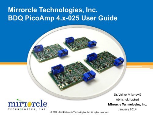
Mirrorcle Technologies, Inc. BDQ PicoAmp 4.x-025 User Guide
Mirrorcle Technologies, Inc. BDQ PicoAmp 4.x-025 User Guide
Mirrorcle Technologies, Inc. BDQ PicoAmp 4.x-025 User Guide

You also want an ePaper? Increase the reach of your titles
YUMPU automatically turns print PDFs into web optimized ePapers that Google loves.
<strong>Mirrorcle</strong> <strong>Technologies</strong>, <strong>Inc</strong>.<br />
<strong>BDQ</strong> <strong>PicoAmp</strong> <strong>4.x</strong>-<strong>025</strong> <strong>User</strong> <strong>Guide</strong><br />
© 2012 - 2014 <strong>Mirrorcle</strong> <strong>Technologies</strong>, <strong>Inc</strong>. All rights reserved.<br />
Dr. Veljko Milanović<br />
Abhishek Kasturi<br />
<strong>Mirrorcle</strong> <strong>Technologies</strong>, <strong>Inc</strong>.<br />
January 2014
Overview<br />
2<br />
Bias Differential Quad-channel (<strong>BDQ</strong>) <strong>PicoAmp</strong> <strong>4.x</strong> is a<br />
compact high voltage amplifier with two analog inputs<br />
and four high voltage analog outputs which also includes<br />
programmable low-pass filters for smoothing of the<br />
output voltages. It is designed and<br />
optimized for the driving of<br />
<strong>Mirrorcle</strong> <strong>Technologies</strong> MEMS<br />
mirrors at voltages up to 140V.<br />
© 2012 - 2014 <strong>Mirrorcle</strong> <strong>Technologies</strong>, <strong>Inc</strong>. All rights reserved.
Features<br />
3<br />
<br />
<br />
<br />
<br />
<br />
<br />
<br />
<br />
<br />
Low voltage supply and low power consumption (
Board Dimensions with Mounting Hole and Connector Locations<br />
4<br />
0<br />
2.54<br />
5.72<br />
0<br />
2.24 mm<br />
J2 – Digikey Part ID: 609-3078-ND<br />
J1 – Digikey Part ID: 609-3530-ND<br />
32.72<br />
38.10<br />
40.64<br />
2.54<br />
10.31<br />
50.95<br />
58.42<br />
60.96<br />
All dimensions are in mm<br />
© 2012 - 2014 <strong>Mirrorcle</strong> <strong>Technologies</strong>, <strong>Inc</strong>. All rights reserved.
Input Connector Pinout and Functions<br />
5<br />
Input: 8 - Pin Header<br />
J1-Pin Name Description<br />
1 EN High Voltage Enable<br />
2 FCLK Filter Clock (60x filter cut-off)<br />
3 GND Ground<br />
4 XIN Analog Input X<br />
5 GND Ground<br />
6 YIN Analog Input Y<br />
7 +5V VDD ( + 5VDC)<br />
8 +5V VDD ( + 5VDC)<br />
© 2012 - 2014 <strong>Mirrorcle</strong> <strong>Technologies</strong>, <strong>Inc</strong>. All rights reserved.
Output Connector Pinout and Functions<br />
6<br />
Output: 8 - Pin Header<br />
J2-Pin Name Description<br />
1 HV_A (X+) High Voltage Output for Channel X+<br />
2 GND Ground<br />
3 HV_B (X-) High Voltage Output for Channel X-<br />
4 GND Ground<br />
5 HV_C (Y-) High Voltage Output for Channel Y-<br />
6 GND Ground<br />
7 HV_D (Y+) High Voltage Output for Channel Y+<br />
8 GND Ground<br />
© 2012 - 2014 <strong>Mirrorcle</strong> <strong>Technologies</strong>, <strong>Inc</strong>. All rights reserved.
Specifications - General<br />
7<br />
Inputs:<br />
VDD: +5VDC<br />
High Voltage Enable: Digital enable/disable for the high voltage supply<br />
Filter Clock:<br />
<strong>User</strong> must provide filter clock for the 5 th Order Bessel low pass filters<br />
The clock (FCLK) can be driven by 3V logic, 50% duty cycle or close<br />
Set clock frequency to the desired filter cut off frequency x 60<br />
• E.g.: Device datasheet states cut off freq. of 1kHz, then FCLK Input = 60kHz<br />
Analog Input X and Y: 0V to 2.5V input<br />
<br />
<br />
<strong>User</strong> applies 1.25V bias input on X and Y as MEMS mirror origin (no tip/tilt)<br />
Deviation from 1.25V results in mirror rotation in positive or negative direction.<br />
Outputs:<br />
HV_A (X+), HV_B (X-), HV_C (Y-), HV_D (Y+): 0V-140V<br />
Low current capability, 100pF) or long cables<br />
© 2012 - 2014 <strong>Mirrorcle</strong> <strong>Technologies</strong>, <strong>Inc</strong>. All rights reserved.
Output Definition<br />
8<br />
HV_A = XIN*56<br />
HV_B = 140-(XIN*56)<br />
HV_C = YIN*56<br />
HV_D = 140-(YIN*56)<br />
Differential Pairs – see next page<br />
© 2012 - 2014 <strong>Mirrorcle</strong> <strong>Technologies</strong>, <strong>Inc</strong>. All rights reserved.
Bi-Directional Driving with Unipolar Voltages<br />
9<br />
HV_B is high<br />
HV_A is low<br />
Mirror rotates in<br />
X- direction<br />
HV_A is high<br />
HV_B is low<br />
Mirror rotates in<br />
X+ direction<br />
Analog Input X<br />
© 2012 - 2014 <strong>Mirrorcle</strong> <strong>Technologies</strong>, <strong>Inc</strong>. All rights reserved.
Specifications - DC Characteristics<br />
10<br />
Supply Current (at VDD = +5VDC)<br />
High Voltage Disabled (Vcc = ~4.5V)<br />
DC Current Supply: ~10mA<br />
High Voltage Enabled (Vcc = ~146V)<br />
DC Current Supply: ~20mA<br />
Supply Voltage<br />
VDD of +5VDC +- 0.4V is required for proper operation<br />
High Voltage Output at 1.25V analog input: ~70V<br />
High voltage stage gain: 56X<br />
Overall High Voltage Output Range: 0V-140V<br />
© 2012 - 2014 <strong>Mirrorcle</strong> <strong>Technologies</strong>, <strong>Inc</strong>. All rights reserved.
Specifications - AC Response<br />
11<br />
<br />
<br />
AC response for this amplifier is determined by the usercontrolled<br />
setting of the low pass filters. The limits for the<br />
embedded 5 th order Bessel filter are 10Hz to 15kHz<br />
frequency-cutoff setting.<br />
The underlying high voltage amplifier circuit has a 25kHz<br />
large signal bandwidth.<br />
© 2012 - 2014 <strong>Mirrorcle</strong> <strong>Technologies</strong>, <strong>Inc</strong>. All rights reserved.
12<br />
SPECIFIC INSTRUCTIONS<br />
<strong>BDQ</strong> <strong>PicoAmp</strong><strong>4.x</strong>
Bringing up <strong>BDQ</strong> <strong>PicoAmp</strong> <strong>4.x</strong><br />
13<br />
1. Turn on the <strong>BDQ</strong> <strong>PicoAmp</strong> by providing VDD and GND to J1.<br />
2. Set the FCLK frequency to control the filter cut-off per recommended<br />
settings for the MEMS mirror connected to the <strong>BDQ</strong> <strong>PicoAmp</strong>.<br />
3. Prior to enabling high voltage, send mirror origin voltage of 1.25V to<br />
analog inputs X and Y.<br />
4. To enable the high voltage, user sends a Digital High through Pin 1 on J1.<br />
WARNING: DO NOT ENABLE HIGH VOLTAGE IF THE X AND Y INPUTS ARE AT NOT SET<br />
AT OR NEAR 1.25V. SUDDEN VOLTAGE DIFFERENCE ON OUTPUT PAIRS MAY<br />
DAMAGE MEMS MIRROR.<br />
5. Now all high voltage outputs X+, X-, Y-, Y+ should be biased at<br />
70V. MEMS mirror may move slightly to a new, ‘biased origin.’ This is<br />
now the new ZERO position for the MEMS mirror.<br />
6. <strong>BDQ</strong> <strong>PicoAmp</strong> is now ready to drive the MEMS mirror to new positions,<br />
waveforms, etc. Although signals are filtered, user should avoid<br />
discontinuous waveforms, steps, and impulses.<br />
WARNING: SEE NEXT PAGE FOR SAFE RANGE OF INPUT VOLTAGES WHEN USING<br />
MIRRORCLE MEMS MIRRORS<br />
© 2012 - 2014 <strong>Mirrorcle</strong> <strong>Technologies</strong>, <strong>Inc</strong>. All rights reserved.
Shutting down <strong>BDQ</strong> <strong>PicoAmp</strong> <strong>4.x</strong><br />
14<br />
1. Send mirror origin voltage of 1.25V to analog inputs X and Y.<br />
2. Disable the high voltage by sending a Digital Low through Pin 1 on J1.<br />
WARNING: DO NOT UNPLUG OR DISABLE ANALOG INPUTS PRIOR TO THIS STEP TO<br />
AVOID APPLYING 0V TO ACTIVE ANALOG INPUTS.<br />
3. Remove power as needed, unplug cables or disable inputs, etc.<br />
© 2012 - 2014 <strong>Mirrorcle</strong> <strong>Technologies</strong>, <strong>Inc</strong>. All rights reserved.
Safe Range of Input Voltages<br />
15<br />
1. Each <strong>Mirrorcle</strong> MEMS Mirror datasheet specifies the<br />
maximum voltage rating (V max ) for a given device on page<br />
1, e.g. 125V.<br />
2. To obtain analog input voltage range:<br />
1. Maximum V in = V max / 56<br />
2. Minimum V in = 2.5 - V max / 56<br />
3. For example above, the maximum input voltage for this<br />
MEMS mirror will be 2.23V<br />
4. The minimum input voltage for this MEMS mirror will be<br />
0.27V<br />
Exceeding these limits may damage the MEMS mirror.<br />
© 2012 - 2014 <strong>Mirrorcle</strong> <strong>Technologies</strong>, <strong>Inc</strong>. All rights reserved.