The Instability of the NbTe2 Surface Structure D - Department of ...
The Instability of the NbTe2 Surface Structure D - Department of ...
The Instability of the NbTe2 Surface Structure D - Department of ...

You also want an ePaper? Increase the reach of your titles
YUMPU automatically turns print PDFs into web optimized ePapers that Google loves.
phys. stat. sol. (a) 193, No. 2, 246–250 (2002)<br />
<strong>The</strong> <strong>Instability</strong> <strong>of</strong> <strong>the</strong> NbTe 2 <strong>Surface</strong> <strong>Structure</strong><br />
D. Cukjati (a), A. Prodan 1 ) (a), N. Jug (a), H. J. P. Van Midden (a),<br />
S. W. Hla (b), H.Böhm (c), F. W. Boswell (d), and J. C. Bennett (e)<br />
(a) Institute Jozef Stefan, Jamova 39, 1000 Ljubljana, Slovenia<br />
(b) <strong>Department</strong> <strong>of</strong> Physics and Astronomy, Ohio University, A<strong>the</strong>ns, OH 45701, USA<br />
(c) Institut für Geowissenschaften, Johannes Gutenberg Universität, 55099 Mainz,<br />
Germany<br />
(d) <strong>Department</strong> <strong>of</strong> Physics, University <strong>of</strong> Waterloo, Waterloo, Ontario, N2L 3G1, Canada<br />
(e) <strong>Department</strong> <strong>of</strong> Physics, Acadia University, Wolfville, Nova Scotia, B0P 1X0, Canada<br />
(Received October 23, 2001; in revised form May 30, 2002; accepted May 30, 2002)<br />
PACS: 61.14.Hg; 68.35.Bs; 68.37.Ef; 68.90.þg<br />
Low energy electron diffraction from clean NbTe 2 surfaces shows very diffuse reflections. <strong>The</strong><br />
effect is attributed to an anisotropic heating <strong>of</strong> <strong>the</strong> irradiated Te–Nb–Te surface layer. Diffraction<br />
patterns for electron energies below 90 eV correspond to an overlapped contribution from numerous<br />
domains, belonging to three orientational variants. Electrons <strong>of</strong> higher energies stabilize <strong>the</strong><br />
parent high-temperature CdI 2 structure. A similar effect is observed during scanning tunneling<br />
microscopy, where <strong>the</strong> expected surface corrugation is usually lost for tunneling currents <strong>of</strong> a few<br />
ten nA.<br />
1. Introduction<br />
NbTe 2 belongs to <strong>the</strong> family <strong>of</strong> layered transition-metal dichalcogenides (MX 2 ), known<br />
for <strong>the</strong>ir quasi two-dimensional character [1] and interesting electronic properties [2]. It<br />
crystallizes in a deformed CdI 2 structure with corrugated Te–Nb–Te sandwiches, separated<br />
by van der Waals (vdW) gaps (Fig. 1). <strong>The</strong> monoclinic structure is built <strong>of</strong><br />
deformed octahedra with two non-equivalent Nb and three non-equivalent Te positions.<br />
Nb atoms are shifted towards one <strong>of</strong> <strong>the</strong> six corners <strong>of</strong> <strong>the</strong> deformed Te octahedra,<br />
which results in an enlarged unit cell with a ¼ 1.939 nm, b ¼ 0.3642 nm, c ¼ 0.9375 nm,<br />
and b ¼ 134 35 0 and in reduced symmetry with <strong>the</strong> space group (SG) C2/m [3]. <strong>The</strong><br />
surface Te atoms form chains at three different heights, aligned along <strong>the</strong> b direction.<br />
Transmission electron microscopy (TEM) and diffraction revealed a domain structure<br />
with three possible orientational variants [4]. <strong>The</strong>se are separated by ortho, meta, and<br />
para boundaries with two adjacent domains forming 60 , 120 , and 180 , respectively. In<br />
addition, anti-phase boundaries, which displace <strong>the</strong> corrugated Te chains along <strong>the</strong><br />
monoclinic a direction by one octahedral chain, were also observed. Scanning tunneling<br />
(STM) and atomic force microscopy <strong>of</strong> <strong>the</strong> corrugated vdW surfaces were performed<br />
[5–7] and it was shown that <strong>the</strong> strong local field between <strong>the</strong> tip and <strong>the</strong> surface<br />
modifies <strong>the</strong> domain boundaries [7].<br />
<strong>The</strong>re were a few reports published on low energy electron diffraction (LEED) studies<br />
<strong>of</strong> <strong>the</strong> MX 2 compounds. It was shown that after Na intercalation into VSe 2 <strong>the</strong><br />
corresponding LEED patterns become only fainter and that no superlattice spots were<br />
1 ) Corresponding author; e-mail: albert.prodan@ijs.si<br />
# 2002 WILEY-VCH Verlag GmbH & Co. KGaA, Weinheim 0031-8965/02/19309-0246 $ 17.50þ.50/0
phys. stat. sol. (a) 193, No. 2 (2002) 247<br />
Fig. 1. Crystal structure <strong>of</strong> NbTe 2 . Layers formed <strong>of</strong> deformed coordination octahedra are separated<br />
by vdW gaps<br />
detected in <strong>the</strong> corresponding LEED patterns [8]. LEED also shows very well charge<br />
density wave (CDW) formation in 1T-TaS 2 and 1T-TaSe 2 . Recently, <strong>the</strong> dependence <strong>of</strong><br />
<strong>the</strong> CDW phases in <strong>the</strong>se compounds on <strong>the</strong> function <strong>of</strong> intercalation [9, 10] and surface<br />
nanostructuring [11, 12] was studied in detail. On <strong>the</strong> contrary, no LEED studies<br />
<strong>of</strong> NbTe 2 or any o<strong>the</strong>r corrugated MX 2 compound were reported so far.<br />
In <strong>the</strong> present paper we show that LEED, combined with STM, provides new information<br />
about <strong>the</strong> stability <strong>of</strong> <strong>the</strong> NbTe 2 surface structure.<br />
2. Experimental<br />
NbTe 2 crystals were grown by iodine transport in evacuated quartz tubes [13] between<br />
1123 and 1073 K. Layered single crystals, a few millimeters large, were obtained after<br />
about a week <strong>of</strong> growth. <strong>The</strong> samples were mounted onto supporting Ta plates with a<br />
graphite paste and cleaved along <strong>the</strong>ir vdW gaps. Freshly cleaved surfaces were examined<br />
under UHV conditions (10 –9 –10 –10 hPa) at room temperature in an Omicron<br />
STM-1, combined with a LEED/Auger spectrometer.<br />
3. Results<br />
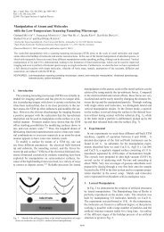
LEED patterns from NbTe 2 with electron energies 80, 89, 100, and 113 eV are shown in<br />
Figs. 2a–d. All images show characteristic diffuse reflections and are fully reproducible<br />
in <strong>the</strong> given energy range, as long as prolonged beam heating does not deteriorate too<br />
much <strong>the</strong> quality <strong>of</strong> <strong>the</strong> examined crystal. Only at energies below about 90 eV <strong>the</strong> patterns<br />
are composed <strong>of</strong> overlapped contributions from domains <strong>of</strong> three orientational<br />
variants. At slightly higher energies <strong>the</strong> reflections characterizing <strong>the</strong> deformation <strong>of</strong><br />
<strong>the</strong> NbTe 2 octahedra disappear and patterns characteristic <strong>of</strong> <strong>the</strong> parent CdI 2 structure<br />
are detected. At energies above about 150 eV all reflections in <strong>the</strong> LEED patterns disappear<br />
and an enhanced background covers <strong>the</strong> entire screen.
248 D. Cukjati et al.: <strong>The</strong> <strong>Instability</strong> <strong>of</strong> <strong>the</strong> NbTe 2 <strong>Surface</strong> <strong>Structure</strong><br />
Fig. 2. Series <strong>of</strong> LEED patterns from <strong>the</strong> NbTe 2<br />
(001) surface for electron energies a) 80, b) 89,<br />
c) 100, and d) 113 eV. <strong>The</strong> additional reflections in<br />
a) correspond to three overlapped orientational<br />
variants<br />
A similar effect was observed in <strong>the</strong> LEED<br />
patterns <strong>of</strong> NbTe 2 if <strong>the</strong> intensity <strong>of</strong> <strong>the</strong> electron<br />
beam was varied between zero and its<br />
maximum value <strong>of</strong> about 2 mA, while <strong>the</strong> energy<br />
<strong>of</strong> <strong>the</strong> electrons was kept constant at<br />
about 90 eV. However, this dependence was<br />
difficult to follow, mainly because <strong>the</strong> already<br />
poor LEED patterns are fur<strong>the</strong>r deteriorated<br />
with reduced beam intensity.<br />
STM images <strong>of</strong> <strong>the</strong> NbTe 2 vdW surfaces<br />
show in addition to surface defects, domain<br />
boundaries, and antiphase boundaries [7] a<br />
characteristic dependence on <strong>the</strong> tunneling current.<br />
At low tunneling currents <strong>the</strong> two uppermost<br />
Te chains are usually not resolved<br />
(Fig. 3a). All three different Te chain types become<br />
clearly distinguished at tunneling currents<br />
<strong>of</strong> a few nA (Fig. 3b), while <strong>the</strong> corrugation<br />
is almost lost for tunneling currents larger<br />
by one order <strong>of</strong> magnitude (Fig. 3c).<br />
4. Discussion<br />
For <strong>the</strong> energies used in <strong>the</strong> described LEED<br />
experiments, <strong>the</strong> penetration depth <strong>of</strong> <strong>the</strong> impinging<br />
electrons fits approximately to <strong>the</strong><br />
thickness <strong>of</strong> one Te–Nb–Te layer [14]. Thus,<br />
<strong>the</strong> origin <strong>of</strong> <strong>the</strong> very diffuse nature <strong>of</strong> <strong>the</strong><br />
NbTe 2 LEED reflections can be ei<strong>the</strong>r in <strong>the</strong><br />
fine domain structure <strong>of</strong> <strong>the</strong> surface layer or in<br />
an enhanced <strong>the</strong>rmal disorder. <strong>The</strong> contribution<br />
<strong>of</strong> both can be estimated.<br />
In case <strong>the</strong> broadening <strong>of</strong> <strong>the</strong> reflections is a<br />
consequence <strong>of</strong> <strong>the</strong> domain structure, <strong>the</strong> average<br />
sizes <strong>of</strong> <strong>the</strong> domains can be estimated by<br />
comparing <strong>the</strong> diameters <strong>of</strong> <strong>the</strong> diffuse reflections<br />
with <strong>the</strong> inter-reflection distances [15]. If<br />
<strong>the</strong> much smaller instrumental contribution is<br />
ignored, <strong>the</strong> broadening corresponds in <strong>the</strong> present case to average domain sizes <strong>of</strong> about<br />
10nm. On <strong>the</strong> contrary, <strong>the</strong> sizes estimated from TEM and STM measurements were
Both LEED and STM studies reveal an unstable surface structure <strong>of</strong> NbTe 2 . It can be<br />
modified by varying <strong>the</strong> energy <strong>of</strong> <strong>the</strong> impinging electrons or <strong>the</strong> intensity <strong>of</strong> <strong>the</strong> elecphys.<br />
stat. sol. (a) 193, No. 2 (2002) 249<br />
Fig. 3. Dependence <strong>of</strong> <strong>the</strong> NbTe 2 STM image on<br />
<strong>the</strong> tunneling conditions. All images were recorded<br />
with <strong>the</strong> constant height mode and with a Pt–Rh<br />
tip: a) (20 nm) 2 , V g ¼ –0.1 mV, I t ¼ 0.8 nA, b)<br />
(10 nm) 2 , V g ¼þ0.1 mV, I t ¼ 2 nA, and c) (10 nm) 2 ,<br />
V g ¼þ0.1 mV, I t ¼ 40 nA<br />
a)<br />
b)<br />
c)<br />
found to be at least an order <strong>of</strong> magnitude larger.<br />
In addition, a similar broadening <strong>of</strong> LEED<br />
reflections is observed in o<strong>the</strong>r transition-metal<br />
dichalcogenides, which do not show any domain<br />
structure. Thus, <strong>the</strong> broadening <strong>of</strong> <strong>the</strong> reflections<br />
is to be attributed to an enhanced <strong>the</strong>rmal<br />
disorder, caused by strongly anisotropic local<br />
heating <strong>of</strong> <strong>the</strong> top Te–Nb–Te layer(s).<br />
<strong>The</strong> diffraction patterns appear for <strong>the</strong> first<br />
time for electron energies between 55 and<br />
80 eV. <strong>The</strong> extinction <strong>of</strong> <strong>the</strong> somewhat weaker<br />
reflections above about 90 eV is likewise to be<br />
attributed to beam heating, which triggers a<br />
transition <strong>of</strong> <strong>the</strong> top Te–Nb–Te layer(s) into<br />
<strong>the</strong> parent high-temperature CdI 2 polytype (SG<br />
P 3 m1). Fur<strong>the</strong>r experiments with <strong>the</strong> intensity<br />
<strong>of</strong> <strong>the</strong> primary beam varied instead <strong>of</strong> <strong>the</strong> electron<br />
energy, support this conclusion. On <strong>the</strong><br />
o<strong>the</strong>r hand, entire bulk samples could not be<br />
heated high enough to achieve <strong>the</strong> transition,<br />
which was an indication that <strong>the</strong> surface regions<br />
are more inclined to undergo <strong>the</strong> described<br />
transition. <strong>The</strong> enhanced background and <strong>the</strong><br />
disappearance <strong>of</strong> all reflections above about<br />
150 eV are a result <strong>of</strong> multiple inelastic electron<br />
scattering, which reduces <strong>the</strong> intensities <strong>of</strong> <strong>the</strong><br />
reflections and enhances <strong>the</strong> background.<br />
Finally, <strong>the</strong> STM images recorded at various<br />
tunneling currents show that <strong>the</strong> structure <strong>of</strong><br />
<strong>the</strong> top Te–Nb–Te triple layer is in a similar<br />
way dependent on <strong>the</strong> strong local field<br />
between <strong>the</strong> tunneling tip and <strong>the</strong> surface,<br />
which can likewise modify <strong>the</strong> observed surface<br />
corrugation.<br />
5. Conclusions
250 D. Cukjati et al.: <strong>The</strong> <strong>Instability</strong> <strong>of</strong> <strong>the</strong> NbTe 2 <strong>Surface</strong> <strong>Structure</strong><br />
tron beam in LEED experiments and by using appropriate tunneling currents in STM<br />
measurements. Both types <strong>of</strong> experiments indicate that at least <strong>the</strong> top Te–Nb–Te triple<br />
layer can be switched between <strong>the</strong> collapsed NbTe 2 and its more symmetrical CdI 2<br />
parent structure. <strong>The</strong> transition is <strong>of</strong> a displacive type and fully reversible as long as <strong>the</strong><br />
quality <strong>of</strong> <strong>the</strong> crystal examined is not deteriorated by prolonged beam heating.<br />
Acknowledgements Financial support <strong>of</strong> <strong>the</strong> Ministry <strong>of</strong> Education, Science, and Sport<br />
<strong>of</strong> <strong>the</strong> Republic <strong>of</strong> Slovenia (D.C., A.P., N.J., H.J.P.v.M.), <strong>of</strong> <strong>the</strong> Deutsche Forschungsgemeinschaft<br />
(H.B.), and <strong>of</strong> <strong>the</strong> Natural Sciences and Engineering Research Council <strong>of</strong><br />
Canada (F.W.B., J.C.B.) is acknowledged. A German–Slovenian joint research program<br />
(H.B., A.P.) and a NATO Expert Visit Grant (A.P., J.C.B.) were helpful in facilitating<br />
<strong>the</strong> collaboration.<br />
References<br />
[1] F. Hulliger, Structural Chemistry <strong>of</strong> Layered-Type Phases, Ed. F. Lévy, Physics and Chemistry<br />
<strong>of</strong> Materials with Layered <strong>Structure</strong>s, D. Reidel Publ. Co., Dordrecht 1976.<br />
[2] M.-H. Whangbo, D.-K. Seo, and E. Canadell, in: Physics and Chemistry <strong>of</strong> Low-Dimensional<br />
Inorganic Conductors, Eds. C. Schlenker, J. Dumas, M. Greenblatt, and S. Van Smaalen,<br />
NATO ASI Series, Series B: Physic Vol. 354, Plenum Press, New York 1996 (pp. 285–302).<br />
[3] B. E. Brown, Acta Crystallogr. 20, 264 (1966).<br />
[4] J. Van Landuyt, G. Remaut, and S. Amelinckx, phys. stat. sol. 41, 271 (1970).<br />
[5] S. N. Magonov and M.-H. Whangbo, <strong>Surface</strong> Analysis with STM and AFM, Experimental and<br />
<strong>The</strong>oretical Aspects <strong>of</strong> Image Analysis, VCH, Weinheim 1996.<br />
[6] R. Wiesendanger and D. Anselmetti, in: Scanning Tunneling Microscopy I, Eds. H.-J. Gün<strong>the</strong>rodt<br />
and R. Wiesendanger, Springer Series in <strong>Surface</strong> Sciences 20, Springer-Verlag, Berlin<br />
1992 (pp. 131–175).<br />
[7] D. Cukjati, A.Prodan, N. Jug, H. J. P. Van Midden, P. Starowicz, E. Karič, S. W. Hla,<br />
H. Böhm, F. W. Boswell, and J. C. Bennett, J. Cryst. Growth 237/239, 278 (2002).<br />
[8] H. E. Brauer, I. Ekvall, H. Olin, H. I. Starnberg, and E. Wahlström, Phys. Rev. B 55, 10022<br />
(1997).<br />
[9] H. J. Crawack, Y. Tomm, and C. Pettenk<strong>of</strong>er, Surf. Sci. 465, 301 (2000).<br />
[10] H. J. Crawack and C. Pettenk<strong>of</strong>er, Solid State Commun. 118, 325 (2001).<br />
[11] R. Adelung, J. Brandt, L. Tarcak, L. Kipp, and M. Skibowski, Appl. Surf. Sci. 162/163, 666<br />
(2000).<br />
[12] R. Adelung, J. Brandt, L. Kipp, and M. Skibowski, Phys. Rev. B 63, 165327 (2001).<br />
[13] H. Shäffer, Chemical Transport Reactions, Academic Press, New York 1964.<br />
[14] H. Luth, <strong>Surface</strong>s and Interfaces <strong>of</strong> Solid Materials, Springer-Verlag, Berlin 1995 (pp. 136–<br />
200).<br />
[15] M. Henzler and W. Göpel, Oberflächenphysik des Festkörpers, Teubner, Stuttgart 1991<br />
(pp. 175–177).