24AA65/24LC65/24C65 64K I2C⢠Smart Serial ... - Microchip
24AA65/24LC65/24C65 64K I2C⢠Smart Serial ... - Microchip
24AA65/24LC65/24C65 64K I2C⢠Smart Serial ... - Microchip

You also want an ePaper? Increase the reach of your titles
YUMPU automatically turns print PDFs into web optimized ePapers that Google loves.
<strong>24AA65</strong>/<strong>24LC65</strong>/<strong>24C65</strong><br />
<strong>64K</strong> I 2 C <strong>Smart</strong> <strong>Serial</strong> EEPROM<br />
Device Selection Table<br />
Part Number VCC Range Page Size Temp. Ranges Packages<br />
<strong>24AA65</strong> 1.8-6.0V 64 Bytes C P, SM<br />
<strong>24LC65</strong> 2.5-6.0V 64 Bytes C, I P, SM<br />
<strong>24C65</strong> 4.5-6.0V 64 Bytes C, I, E P, SM<br />
Features<br />
• Voltage operating range: 1.8V to 6.0V<br />
- Peak write current 3 mA at 6.0V<br />
- Maximum read current 150 µA at 6.0V<br />
- Standby current 1 µA typical<br />
• Industry standard two-wire bus protocol I 2 C<br />
compatible<br />
• 8-byte page, or byte modes available<br />
• 2 ms typical write cycle time, byte or page<br />
• 64-byte input cache for fast write loads<br />
• Up to 8 devices may be connected to the same<br />
bus for up to 512K bits total memory<br />
• Including 100 kHz (1.8V ≤ Vcc < 4.5V) and 400<br />
kHz (4.5V ≤ VCC ≤ 6.0V) compatibility<br />
• Programmable block security options<br />
• Programmable endurance options<br />
• Schmitt Trigger, filtered inputs for noise<br />
suppression<br />
• Output slope control to eliminate ground bounce<br />
• Self-timed erase and write cycles<br />
• Power-on/off data protection circuitry<br />
• Endurance:<br />
- 10,000,000 E/W cycles for a High Endurance<br />
Block<br />
- 1,000,000 E/W cycles for a Standard<br />
Endurance Block<br />
• Electrostatic discharge protection > 4000V<br />
• Data retention > 200 years<br />
• 8-pin PDIP/SOIC packages<br />
• Temperature ranges<br />
- Commercial (C): 0°C to +70°C<br />
- Industrial (I) -40°C to +85°C<br />
- Automotive (E) -40°C to +125°C<br />
Description<br />
The <strong>Microchip</strong> Technology Inc. <strong>24AA65</strong>/<strong>24LC65</strong>/<br />
<strong>24C65</strong> (24XX65)* is a “smart” 8K x 8 <strong>Serial</strong> Electrically<br />
Erasable PROM. This device has been developed for<br />
advanced, low-power applications such as personal<br />
communications, and provides the systems designer<br />
with flexibility through the use of many new user-programmable<br />
features. The 24XX65 offers a relocatable<br />
4K bit block of ultra-high-endurance memory for data<br />
that changes frequently. The remainder of the array, or<br />
60K bits, is rated at 1,000,000 erase/write (E/W) cycles<br />
ensured. The 24XX65 features an input cache for fast<br />
write loads with a capacity of eight pages, or 64 bytes.<br />
This device also features programmable security<br />
options for E/W protection of critical data and/or code<br />
of up to fifteen 4K blocks. Functional address lines<br />
allow the connection of up to eight 24XX65's on the<br />
same bus for up to 512K bits contiguous EEPROM<br />
memory. Advanced CMOS technology makes this<br />
device ideal for low-power nonvolatile code and data<br />
applications. The 24XX65 is available in the standard<br />
8-pin plastic DIP and 8-pin surface mount SOIC<br />
package.<br />
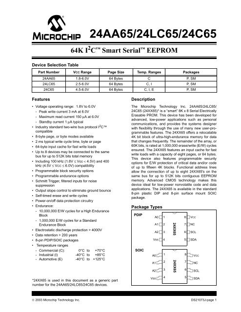
Package Types<br />
PDIP<br />
SOIC<br />
A0<br />
A1<br />
A2<br />
VSS<br />
A0<br />
A1<br />
A2<br />
1<br />
2<br />
3<br />
4<br />
1<br />
2<br />
3<br />
24XX65<br />
24XX65<br />
8<br />
7<br />
6<br />
5<br />
8<br />
7<br />
6<br />
VCC<br />
NC<br />
SCL<br />
SDA<br />
VCC<br />
NC<br />
SCL<br />
*24XX65 is used in this document as a generic part<br />
number for the <strong>24AA65</strong>/<strong>24LC65</strong>/<strong>24C65</strong> devices.<br />
VSS<br />
4<br />
5<br />
SDA<br />
© 2003 <strong>Microchip</strong> Technology Inc. DS21073J-page 1
<strong>24AA65</strong>/<strong>24LC65</strong>/<strong>24C65</strong><br />
Block Diagram<br />
Pin Function Table<br />
A0 A1 A2<br />
HV Generator<br />
Name<br />
Function<br />
A0, A1, A2 User Configurable Chip Selects<br />
I/O<br />
Control<br />
Logic<br />
Memory<br />
Control<br />
Logic<br />
XDEC<br />
EEPROM<br />
Array<br />
Page Latches<br />
VSS<br />
SDA<br />
SCL<br />
VCC<br />
Ground<br />
<strong>Serial</strong> Address/Data/I/O<br />
<strong>Serial</strong> Clock<br />
+1.8V to 6.0V Power Supply<br />
I/O<br />
SCL<br />
Cache<br />
NC<br />
No Internal Connection<br />
SDA<br />
YDEC<br />
VCC<br />
VSS<br />
Sense Amp.<br />
R/W Control<br />
DS21073J-page 2<br />
© 2003 <strong>Microchip</strong> Technology Inc.
<strong>24AA65</strong>/<strong>24LC65</strong>/<strong>24C65</strong><br />
1.0 ELECTRICAL CHARACTERISTICS<br />
Absolute Maximum Ratings (†)<br />
VCC.............................................................................................................................................................................7.0V<br />
All inputs and outputs w.r.t. VSS ..........................................................................................................-0.6V to VCC +1.0V<br />
Storage temperature ...............................................................................................................................-65°C to +150°C<br />
Ambient temperature with power applied................................................................................................-65°C to +125°C<br />
ESD protection on all pins ......................................................................................................................................................≥ 4 kV<br />
† NOTICE: Stresses above those listed under “Absolute Maximum Ratings” may cause permanent damage to the<br />
device. This is a stress rating only and functional operation of the device at those or any other conditions above those<br />
indicated in the operational listings of this specification is not implied. Exposure to maximum rating conditions for an<br />
extended period of time may affect device reliability.<br />
TABLE 1-1:<br />
DC CHARACTERISTICS<br />
DC CHARACTERISTICS<br />
VCC = +1.8V to +6.0V<br />
Commercial (C): TA = 0°C to +70°C<br />
Industrial (I): TA = -40°C to +85°C<br />
Automotive (E): TA = -40°C to +125°C<br />
Parameter Sym Min Max Units Conditions<br />
A0, A1, A2, SCL and SDA pins:<br />
High-level input voltage<br />
Low-level input voltage<br />
Hysteresis of Schmitt Trigger inputs<br />
Low-level output voltage<br />
VIH<br />
VIL<br />
VHYS<br />
VOL<br />
.7 VCC<br />
—<br />
.05 VCC<br />
—<br />
—<br />
.3 VCC<br />
—<br />
.40<br />
V<br />
V<br />
V<br />
V<br />
(Note 1)<br />
IOL = 3.0 mA<br />
Input leakage current ILI — ±1 µA VIN = .1V to VCC<br />
Output leakage current ILO — ±1 µA VOUT = .1V to VCC<br />
Pin capacitance<br />
(all inputs/outputs)<br />
Operating current<br />
CIN, COUT — 10 pF VCC = 5.0V (Note 1)<br />
TA = 25°C, FCLK = 1 MHz<br />
ICC Write<br />
ICC Read<br />
—<br />
—<br />
3<br />
150<br />
mA<br />
µA<br />
VCC = 6.0V, SCL = 400 kHz<br />
VCC = 6.0V, SCL = 400 kHz<br />
Standby current ICCS — 5 µA VCC = 5.0V, SCL = SDA = VCC<br />
A0, A1, A2 = VSS<br />
Note 1: This parameter is periodically sampled and not 100% tested.<br />
FIGURE 1-1:<br />
BUS TIMING START/STOP<br />
VHYS<br />
SCL<br />
SDA<br />
TSU:STA<br />
THD:STA<br />
TSU:STO<br />
START<br />
STOP<br />
© 2003 <strong>Microchip</strong> Technology Inc. DS21073J-page 3
<strong>24AA65</strong>/<strong>24LC65</strong>/<strong>24C65</strong><br />
TABLE 1-2:<br />
AC CHARACTERISTICS<br />
VCC = 1.8V-6.0V<br />
STD. Mode<br />
VCC = 4.5-6.0V<br />
FAST Mode Units Remarks<br />
Parameter<br />
Symbol<br />
Min Max Min Max<br />
Clock frequency FCLK — 100 — 400 kHz<br />
Clock high time THIGH 4000 — 600 — ns<br />
Clock low time TLOW 4700 — 1300 — ns<br />
SDA and SCL rise time TR — 1000 — 300 ns (Note 1)<br />
SDA and SCL fall time TF — 300 — 300 ns (Note 1)<br />
Start condition setup time THD:STA 4000 — 600 — ns After this period the first<br />
clock pulse is generated<br />
Start condition setup time TSU:STA 4700 — 600 — ns Only relevant for<br />
repeated Start condition<br />
Data input hold time THD:DAT 0 — 0 — ns<br />
Data input setup time TSU:DAT 250 — 100 — ns<br />
Stop condition setup time TSU:STO 4000 — 600 — ns<br />
Output valid from clock TAA — 3500 — 900 ns (Note 2)<br />
Bus free time TBUF 4700 — 1300 — ns Time the bus must be<br />
free before a new<br />
transmission can start<br />
Output fall time from VIH min to TOF — 250 20 + 0.1 250 ns (Note 1), CB ≤ 100 pF<br />
VIL max<br />
CB<br />
Input filter spike suppression TSP 50 — 50 — ns (Note 3)<br />
(SDA and SCL pins)<br />
Write cycle time TWR — 5 — 5 ms/page (Note 4)<br />
Endurance<br />
High Endurance Block<br />
Rest of Array<br />
Note 1:<br />
10M<br />
1M<br />
—<br />
—<br />
10M<br />
1M<br />
—<br />
—<br />
cycles 25°C, (Note 5)<br />
Not 100 percent tested. CB = total capacitance of one bus line in pF.<br />
2: As a transmitter, the device must provide an internal minimum delay time to bridge the undefined region<br />
(minimum 300 ns) of the falling edge of SCL to avoid unintended generation of Start or Stop conditions.<br />
3: The combined TSP and VHYS specifications are due to new Schmitt Trigger inputs which provide improved<br />
noise and spike suppression. This eliminates the need for a Ti specification for standard operation.<br />
4: The times shown are for a single page of 8 bytes. Multiply by the number of pages loaded into the write<br />
cache for total time.<br />
5: This parameter is not tested but ensured by characterization. For endurance estimates in a specific<br />
application, please consult the Total Endurance Model which can be downloaded at www.microchip.com.<br />
FIGURE 1-2:<br />
BUS TIMING DATA<br />
TF<br />
THIGH<br />
TR<br />
TLOW<br />
SCL<br />
TSU:STA<br />
THD:STA<br />
THD:DAT TSU:DAT<br />
TSU:STO<br />
SDA<br />
IN<br />
TSP<br />
TAA<br />
TAA<br />
TBUF<br />
SDA<br />
OUT<br />
DS21073J-page 4<br />
© 2003 <strong>Microchip</strong> Technology Inc.
<strong>24AA65</strong>/<strong>24LC65</strong>/<strong>24C65</strong><br />
2.0 FUNCTIONAL DESCRIPTION<br />
The 24XX65 supports a bidirectional two-wire bus and<br />
data transmission protocol. A device that sends data<br />
onto the bus is defined as transmitter, and a device<br />
receiving data as receiver. The bus must be controlled<br />
by a master device which generates the serial clock<br />
(SCL), controls the bus access and generates the Start<br />
and Stop conditions, while the 24XX65 works as slave.<br />
Both master and slave can operate as transmitter or<br />
receiver, but the master device determines which mode<br />
is activated.<br />
3.0 BUS CHARACTERISTICS<br />
The following bus protocol has been defined:<br />
• Data transfer may be initiated only when the bus<br />
is not busy.<br />
• During data transfer, the data line must remain<br />
stable whenever the clock line is high. Changes in<br />
the data line while the clock line is high will be<br />
interpreted as a Start or Stop condition.<br />
Accordingly, the following bus conditions have been<br />
defined (Figure 3-1).<br />
3.1 Bus not Busy (A)<br />
Both data and clock lines remain high.<br />
3.2 Start Data Transfer (B)<br />
A high-to-low transition of the SDA line while the clock<br />
(SCL) is high determines a Start condition. All<br />
commands must be preceded by a Start condition.<br />
3.3 Stop Data Transfer (C)<br />
A low-to-high transition of the SDA line while the clock<br />
(SCL) is high determines a Stop condition. All<br />
operations must be ended with a Stop condition.<br />
3.4 Data Valid (D)<br />
The state of the data line represents valid data when,<br />
after a Start condition, the data line is stable for the<br />
duration of the high period of the clock signal.<br />
The data on the line must be changed during the low<br />
period of the clock signal. There is one clock pulse per<br />
bit of data.<br />
Each data transfer is initiated with a Start condition and<br />
terminated with a Stop condition. The number of the<br />
data bytes transferred between the Start and Stop<br />
conditions is determined by the master device.<br />
3.5 Acknowledge<br />
Each receiving device, when addressed, is obliged to<br />
generate an acknowledge after the reception of each<br />
byte. The master device must generate an extra clock<br />
pulse which is associated with this Acknowledge bit.<br />
Note:<br />
The 24XX65 does not generate any<br />
Acknowledge bits if an internal programming<br />
cycle is in progress.<br />
A device that acknowledges must pull down the SDA<br />
line during the Acknowledge clock pulse in such a way<br />
that the SDA line is stable low during the high period of<br />
the acknowledge related clock pulse. Of course, setup<br />
and hold times must be taken into account. During<br />
reads, a master must signal an end of data to the slave<br />
by NOT generating an Acknowledge bit on the last byte<br />
that has been clocked out of the slave. In this case, the<br />
slave (24XX65) must leave the data line high to enable<br />
the master to generate the Stop condition.<br />
FIGURE 3-1:<br />
DATA TRANSFER SEQUENCE ON THE SERIAL BUS<br />
SCL<br />
(A) (B) (D) (D) (C) (A)<br />
SDA<br />
Start<br />
Condition<br />
Address or<br />
Acknowledge<br />
Valid<br />
Data<br />
Allowed<br />
To Change<br />
Stop<br />
Condition<br />
© 2003 <strong>Microchip</strong> Technology Inc. DS21073J-page 5
<strong>24AA65</strong>/<strong>24LC65</strong>/<strong>24C65</strong><br />
3.6 Device Addressing<br />
A control byte is the first byte received following the<br />
Start condition from the master device. The control byte<br />
consists of a four-bit control code, for the 24XX65 this<br />
is set as ‘1010’ binary for read and write operations.<br />
The next three bits of the control byte are the device<br />
select bits (A2, A1, A0). They are used by the master<br />
device to select which of the eight devices are to be<br />
accessed. These bits are in effect the three Most<br />
Significant bits of the word address. The last bit of the<br />
control byte defines the operation to be performed.<br />
When set to a one a read operation is selected, when<br />
set to a zero a write operation is selected. The next two<br />
bytes received define the address of the first data byte<br />
(Figure 4-1). Because only A12..A0 are used, the<br />
upper three address bits must be zeros. The Most<br />
Significant bit of the Most Significant Byte is transferred<br />
first. Following the Start condition, the 24XX65<br />
monitors the SDA bus checking the device type<br />
identifier being transmitted. Upon receiving a ‘1010’<br />
code and appropriate device select bits, the slave<br />
device (24XX65) outputs an Acknowledge signal on the<br />
SDA line. Depending upon the state of the R/W bit, the<br />
24XX65 will select a read or write operation.<br />
Operation Control Code Device Select R/W<br />
Read 1010 Device Address 1<br />
Write 1010 Device Address 0<br />
FIGURE 3-2:<br />
START<br />
CONTROL BYTE<br />
ALLOCATION<br />
SLAVE ADDRESS<br />
READ/WRITE<br />
R/W<br />
1 0 1 0 A2 A1 A0<br />
A<br />
4.0 WRITE OPERATION<br />
4.1 Byte Write<br />
Following the Start condition from the master, the control<br />
code (four bits), the device select (three bits), and<br />
the R/W bit which is a logic low, is placed onto the bus<br />
by the master transmitter. This indicates to the<br />
addressed slave receiver (24XX65) that a byte with a<br />
word address will follow after it has generated an<br />
Acknowledge bit during the ninth clock cycle. Therefore,<br />
the next byte transmitted by the master is the<br />
high-order byte of the word address and will be written<br />
into the address pointer of the 24XX65. The next byte<br />
is the Least Significant Address Byte. After receiving<br />
another Acknowledge signal from the 24XX65, the<br />
master device will transmit the data word to be written<br />
into the addressed memory location. The 24XX65<br />
acknowledges again and the master generates a Stop<br />
condition. This initiates the internal write cycle, and<br />
during this time the 24XX65 will not generate<br />
Acknowledge signals (Figure 4-1).<br />
4.2 Page Write<br />
The write control byte, word address and the first data<br />
byte are transmitted to the 24XX65 in the same way as<br />
in a byte write. But instead of generating a Stop<br />
condition, the master transmits up to eight pages of<br />
eight data bytes each (64 bytes total), which are<br />
temporarily stored in the on-chip page cache of the<br />
24XX65. They will be written from the cache into the<br />
EEPROM array after the master has transmitted a Stop<br />
condition. After the receipt of each word, the six lower<br />
order address pointer bits are internally incremented by<br />
one. The higher order seven bits of the word address<br />
remain constant. If the master should transmit more<br />
than eight bytes prior to generating the Stop condition<br />
(writing across a page boundary), the address counter<br />
(lower three bits) will roll over and the pointer will be<br />
incremented to point to the next line in the cache. This<br />
can continue to occur up to eight times or until the cache<br />
is full, at which time a Stop condition should be<br />
generated by the master. If a Stop condition is not<br />
received, the cache pointer will roll over to the first line<br />
(byte 0) of the cache, and any further data received will<br />
overwrite previously captured data. The Stop condition<br />
can be sent at any time during the transfer. As with the<br />
byte write operation, once the Stop condition is received<br />
an internal write cycle will begin. The 64-byte cache will<br />
continue to capture data until a Stop condition occurs or<br />
the operation is aborted (Figure 4-2).<br />
DS21073J-page 6<br />
© 2003 <strong>Microchip</strong> Technology Inc.
<strong>24AA65</strong>/<strong>24LC65</strong>/<strong>24C65</strong><br />
FIGURE 4-1:<br />
BUS ACTIVITY<br />
MASTER<br />
BYTE WRITE<br />
S<br />
T<br />
A<br />
R<br />
T<br />
CONTROL<br />
BYTE<br />
WORD<br />
ADDRESS (1)<br />
WORD<br />
ADDRESS (0)<br />
DATA<br />
S<br />
T<br />
O<br />
P<br />
SDA LINE<br />
S<br />
000<br />
P<br />
BUS ACTIVITY<br />
A<br />
C<br />
K<br />
A<br />
C<br />
K<br />
A<br />
C<br />
K<br />
A<br />
C<br />
K<br />
FIGURE 4-2: PAGE WRITE (FOR CACHE WRITE, SEE FIGURE 8-2)<br />
S<br />
T<br />
A<br />
BUS<br />
ACTIVITY<br />
MASTER<br />
CONTROL<br />
BYTE<br />
WORD<br />
ADDRESS (1)<br />
S<br />
T<br />
O<br />
P<br />
SDA LINE S<br />
R<br />
T<br />
A<br />
CK<br />
0<br />
WORD<br />
ADDRESS (0)<br />
DATA n DATA n + 7<br />
0 0<br />
P<br />
BUS<br />
ACTIVITY:<br />
A<br />
C<br />
K<br />
A<br />
CK<br />
A<br />
C<br />
K<br />
A<br />
CK<br />
FIGURE 4-3:<br />
CURRENT ADDRESS READ<br />
BUS ACTIVITY<br />
MASTER<br />
S<br />
T<br />
A<br />
R<br />
T<br />
CONTROL<br />
BYTE<br />
DATA n<br />
S<br />
T<br />
O<br />
P<br />
SDA LINE<br />
S<br />
P<br />
BUS ACTIVITY<br />
A<br />
C<br />
K<br />
N<br />
O<br />
A<br />
C<br />
K<br />
© 2003 <strong>Microchip</strong> Technology Inc. DS21073J-page 7
<strong>24AA65</strong>/<strong>24LC65</strong>/<strong>24C65</strong><br />
FIGURE 4-4:<br />
RANDOM READ<br />
S<br />
T<br />
A<br />
R<br />
T<br />
CONTROL<br />
BYTE<br />
WORD<br />
ADDRESS (1)<br />
WORD<br />
ADDRESS (0)<br />
S<br />
T<br />
A<br />
R<br />
T<br />
CONTROL<br />
BYTE<br />
DATA n<br />
S<br />
T<br />
O<br />
P<br />
SDA LINE S<br />
BUS<br />
ACTIVITY<br />
0 0 0<br />
A<br />
C<br />
K<br />
A<br />
CK<br />
A<br />
CK<br />
S<br />
A<br />
C<br />
K<br />
P<br />
N<br />
O<br />
A<br />
C<br />
K<br />
FIGURE 4-5:<br />
BUS ACTIVITY<br />
MASTER<br />
SEQUENTIAL READ<br />
CONTROL<br />
BYTE<br />
DATA n DATA n + 1 DATA n + 2 DATA n + X<br />
S<br />
T<br />
O<br />
P<br />
SDA LINE<br />
P<br />
BUS ACTIVITY<br />
A<br />
C<br />
K<br />
A<br />
C<br />
K<br />
A<br />
C<br />
K<br />
A<br />
C<br />
K<br />
N<br />
O<br />
A<br />
C<br />
K<br />
DS21073J-page 8<br />
© 2003 <strong>Microchip</strong> Technology Inc.
<strong>24AA65</strong>/<strong>24LC65</strong>/<strong>24C65</strong><br />
5.0 READ OPERATION<br />
Read operations are initiated in the same way as write<br />
operations with the exception that the R/W bit of the<br />
slave address is set to one. There are three basic types<br />
of read operations: current address read, random read<br />
and sequential read.<br />
5.1 Current Address Read<br />
The 24XX65 contains an address counter that maintains<br />
the address of the last word accessed, internally<br />
incremented by one. Therefore, if the previous access<br />
(either a read or write operation) was to address n (n is<br />
any legal address), the next current address read<br />
operation would access data from address n + 1. Upon<br />
receipt of the slave address with R/W bit set to one, the<br />
24XX65 issues an acknowledge and transmits the<br />
eight-bit data word. The master will not acknowledge<br />
the transfer but does generate a Stop condition and the<br />
24XX65 discontinues transmission (Figure 4-3).<br />
5.2 Random Read<br />
Random read operations allow the master to access<br />
any memory location in a random manner. To perform<br />
this type of read operation, first the word address must<br />
be set. This is done by sending the word address to the<br />
24XX65 as part of a write operation (R/W bit set to ‘0’).<br />
After the word address is sent, the master generates a<br />
Start condition following the acknowledge. This<br />
terminates the write operation, but not before the<br />
internal address pointer is set. Then the master issues<br />
the control byte again, but with the R/W bit set to a one.<br />
The 24XX65 will then issue an acknowledge and<br />
transmit the eight-bit data word. The master will not<br />
acknowledge the transfer, but does generate a Stop<br />
condition which causes the 24XX65 to discontinue<br />
transmission (Figure 4-4).<br />
5.4 Contiguous Addressing Across<br />
Multiple Devices<br />
The device select bits A2, A1, A0 can be used to<br />
expand the contiguous address space for up to 512K<br />
bits by adding up to eight 24XX65's on the same bus.<br />
In this case, software can use A0 of the control byte as<br />
address bit A13, A1 as address bit A14 and A2 as<br />
address bit A15.<br />
5.5 Noise Protection<br />
The SCL and SDA inputs have filter circuits which<br />
suppress noise spikes to assure proper device<br />
operation even on a noisy bus. All I/O lines incorporate<br />
Schmitt Triggers for 400 kHz (Fast mode) compatibility.<br />
5.6 High Endurance Block<br />
The location of the high endurance block within the<br />
memory map is programmed by setting the leading bit<br />
7 (S/HE) of the configuration byte to ‘0’. The upper bits<br />
of the address loaded in this command will determine<br />
which 4K block within the memory map will be set to<br />
high endurance. This block will be capable of<br />
10,000,000 erase/write cycles typical (Figure 8-1).<br />
The high endurance block will retain its value as the<br />
high endurance block even if it resides within the<br />
security block range. The high endurance setting<br />
always takes precedence to the security setting.<br />
Note:<br />
The high endurance block cannot be<br />
changed after the security option has been<br />
set with a length greater than zero. If the<br />
H.E. block is not programmed by the user,<br />
the default location is the highest block of<br />
memory which starts at location 0x1E00<br />
and ends at 0x1FFF.<br />
5.3 Sequential Read<br />
Sequential reads are initiated in the same way as a<br />
random read except that after the 24XX65 transmits the<br />
first data byte, the master issues an acknowledge as<br />
opposed to the Stop condition used in a random read.<br />
This acknowledge directs the 24XX65 to transmit the<br />
next sequentially addressed 8-bit word (Figure 4-5).<br />
Following the final byte transmitted to the master, the<br />
master will NOT generate an acknowledge, but will<br />
generate a Stop condition.<br />
To provide sequential reads the 24XX65 contains an<br />
internal address pointer which is incremented by one at<br />
the completion of each operation. This address pointer<br />
allows the entire memory contents to be serially read<br />
during one operation.<br />
© 2003 <strong>Microchip</strong> Technology Inc. DS21073J-page 9
<strong>24AA65</strong>/<strong>24LC65</strong>/<strong>24C65</strong><br />
5.7 Security Options<br />
The 24XX65 has a sophisticated mechanism for write<br />
protecting portions of the array. This write-protect<br />
function is programmable and allows the user to protect<br />
0-15 contiguous 4K blocks. The user sets the security<br />
option by sending to the device the starting block<br />
number for the protected region and the number of<br />
blocks to be protected. All parts will come from the<br />
factory in the default configuration with the starting<br />
block number set to 15 and the number of protected<br />
blocks set to zero. THE SECURITY OPTION CAN BE<br />
SET ONLY ONCE WITH A LENGTH GREATER THAN<br />
ZERO.<br />
To invoke the security option, a Write command is sent<br />
to the device with the leading bit (bit 7) of the first<br />
address byte set to a ‘1’ (Figure 8-1). Bits 1-4 of the first<br />
address byte define the starting block number for the<br />
protected region.<br />
For example, if the starting block number is to be set to<br />
5, the first address byte would be 1XX0101X. Bits 0, 5<br />
and 6 of the first address byte are disregarded by the<br />
device and can be either high or low. The device will<br />
acknowledge after the first address byte. A byte of don’t<br />
care bits is then sent by the master, with the device<br />
acknowledging afterwards. The third byte sent to the<br />
device has bit 7 (S/HE) set high and bit 6 (R) set low.<br />
Bits 4 and 5 are don’t cares and bits 0-3 define the<br />
number of blocks to be write-protected. For example, if<br />
three blocks are to be protected, the third byte would be<br />
10XX0011. After the third byte is sent to the device, it<br />
will acknowledge and a Stop bit is then sent by the master<br />
to complete the command.<br />
If one of the security blocks coincides with the high<br />
endurance block, the high endurance setting will take<br />
precedence. Also, if the range of the security blocks<br />
encompass the high endurance block when the security<br />
option is set, the security block range will be set<br />
accordingly, but the high endurance block will continue<br />
to retain the high endurance setting. As a result, the<br />
memory blocks preceding the high endurance block will<br />
be set as secure sections.<br />
During a normal write sequence, if an attempt is made<br />
to write to a protected address, no data will be written<br />
and the device will not report an error or abort the<br />
command. If a Write command is attempted across a<br />
secure boundary, unprotected addresses will be written<br />
and protected addresses will not.<br />
5.8 Security Configuration Read<br />
The status of the secure portion of memory can be read<br />
by using the same technique as programming this<br />
option except the read bit (bit 6) of the configuration<br />
byte is set to a one. After the configuration byte is sent,<br />
the device will acknowledge and then send two bytes of<br />
data to the master just as in a normal read sequence.<br />
The master must acknowledge the first byte and not<br />
acknowledge the second, and then send a Stop bit to<br />
end the sequence. The upper four bits of both of these<br />
bytes will always be read as ‘1’s. The lower four bits of<br />
the first byte contains the starting secure block. The<br />
lower four bits of the second byte contains the number<br />
of secure blocks. The default starting secure block is<br />
fifteen and the default number of secure blocks is zero<br />
(Figure 8-1).<br />
6.0 ACKNOWLEDGE POLLING<br />
Since the device will not acknowledge during a write<br />
cycle, this can be used to determine when the cycle is<br />
complete (this feature can be used to maximize bus<br />
throughput). Once the Stop condition for a Write<br />
command has been issued from the master, the device<br />
initiates the internally timed write cycle. ACK polling<br />
can be initiated immediately. This involves the master<br />
sending a Start condition followed by the control byte<br />
for a Write command (R/W = 0). If the device is still<br />
busy with the write cycle, then no ACK will be returned.<br />
If the cycle is complete, then the device will return the<br />
ACK and the master can then proceed with the next<br />
Read or Write command. See Figure 6-1 for flow<br />
diagram.<br />
FIGURE 6-1:<br />
ACKNOWLEDGE<br />
POLLING FLOW<br />
Send<br />
Write Command<br />
Send Stop<br />
Condition to<br />
Initiate Write Cycle<br />
Send Start<br />
Send Control Byte<br />
with R/W = 0<br />
Did Device<br />
Acknowledge<br />
(ACK = 0)?<br />
YES<br />
Next<br />
Operation<br />
NO<br />
DS21073J-page 10<br />
© 2003 <strong>Microchip</strong> Technology Inc.
<strong>24AA65</strong>/<strong>24LC65</strong>/<strong>24C65</strong><br />
7.0 PAGE CACHE AND ARRAY<br />
MAPPING<br />
The cache is a 64-byte (8 pages x 8 bytes) FIFO buffer.<br />
The cache allows the loading of up to 64 bytes of data<br />
before the write cycle is actually begun, effectively<br />
providing a 64-byte burst write at the maximum bus<br />
rate. Whenever a Write command is initiated, the cache<br />
starts loading and will continue to load until a Stop bit is<br />
received to start the internal write cycle. The total<br />
length of the write cycle will depend on how many<br />
pages are loaded into the cache before the Stop bit is<br />
given. Maximum cycle time for each page is 5 ms. Even<br />
if a page is only partially loaded, it will still require the<br />
same cycle time as a full page. If more than 64 bytes of<br />
data are loaded before the Stop bit is given, the<br />
address pointer will ‘wrap around’ to the beginning of<br />
cache page 0 and existing bytes in the cache will be<br />
overwritten. The device will not respond to any<br />
commands while the write cycle is in progress.<br />
7.1 Cache Write Starting at a Page<br />
Boundary<br />
If a Write command begins at a page boundary<br />
(address bits A2, A1 and A0 are zero), then all data<br />
loaded into the cache will be written to the array in<br />
sequential addresses. This includes writing across a<br />
4K block boundary. In the example shown below,<br />
(Figure 8-2) a Write command is initiated starting at<br />
byte 0 of page 3 with a fully loaded cache (64 bytes).<br />
The first byte in the cache is written to byte 0 of page 3<br />
(of the array), with the remaining pages in the cache<br />
written to sequential pages in the array. A write cycle is<br />
executed after each page is written. Since the write<br />
begins at page 3 and 8 pages are loaded into the<br />
cache, the last 3 pages of the cache are written to the<br />
next row in the array.<br />
7.2 Cache Write Starting at a<br />
Non-Page Boundary<br />
When a Write command is initiated that does not begin<br />
at a page boundary (i.e., address bits A2, A1 and A0<br />
are not all zero), it is important to note how the data is<br />
loaded into the cache, and how the data in the cache is<br />
written to the array. When a Write command begins, the<br />
first byte loaded into the cache is always loaded into<br />
page 0. The byte within page 0 of the cache where the<br />
load begins is determined by the three Least Significant<br />
Address bits (A2, A1, A0) that were sent as part of the<br />
Write command. If the Write command does not start at<br />
byte 0 of a page and the cache is fully loaded, then the<br />
last byte(s) loaded into the cache will roll around to<br />
page 0 of the cache and fill the remaining empty bytes.<br />
If more than 64 bytes of data are loaded into the cache,<br />
data already loaded will be overwritten. In the example<br />
shown in Figure 8-3, a Write command has been<br />
initiated starting at byte 2 of page 3 in the array with a<br />
fully loaded cache of 64 bytes. Since the cache started<br />
loading at byte 2, the last two bytes loaded into the<br />
cache will ‘roll over' and be loaded into the first two<br />
bytes of page 0 (of the cache). When the Stop bit is<br />
sent, page 0 of the cache is written to page 3 of the<br />
array. The remaining pages in the cache are then<br />
loaded sequentially to the array. A write cycle is<br />
executed after each page is written. If a partially loaded<br />
page in the cache remains when the Stop bit is sent,<br />
only the bytes that have been loaded will be written to<br />
the array.<br />
7.3 Power Management<br />
The design incorporates a power Standby mode when<br />
not in use and automatically powers off after the normal<br />
termination of any operation when a Stop bit is received<br />
and all internal functions are complete. This includes<br />
any error conditions (i.e., not receiving an Acknowledge<br />
or Stop condition per the two-wire bus specification).<br />
The device also incorporates VDD monitor<br />
circuitry to prevent inadvertent writes (data corruption)<br />
during low voltage conditions. The VDD monitor circuitry<br />
is powered off when the device is in Standby mode in<br />
order to further reduce power consumption.<br />
8.0 PIN DESCRIPTIONS<br />
8.1 A0, A1, A2 Chip Address Inputs<br />
The A0..A2 inputs are used by the 24XX65 for multiple<br />
device operation and conform to the two-wire bus<br />
standard. The levels applied to these pins define the<br />
address block occupied by the device in the address<br />
map. A particular device is selected by transmitting the<br />
corresponding bits (A2, A1, A0) in the control byte<br />
(Figure 3-2 and Figure 8-1).<br />
8.2 SDA <strong>Serial</strong> Address/Data Input/<br />
Output<br />
This is a bidirectional pin used to transfer addresses<br />
and data into and data out of the device. It is an open<br />
drain terminal, therefore the SDA bus requires a pull-up<br />
resistor to VCC (typical 10 KΩ for 100 kHz, 2 KΩ for 400<br />
kHz).<br />
For normal data transfer SDA is allowed to change only<br />
during SCL low. Changes during SCL high are<br />
reserved for indicating the Start and Stop conditions.<br />
8.3 SCL <strong>Serial</strong> Clock<br />
This input is used to synchronize the data transfer from<br />
and to the device.<br />
© 2003 <strong>Microchip</strong> Technology Inc. DS21073J-page 11
<strong>24AA65</strong>/<strong>24LC65</strong>/<strong>24C65</strong><br />
FIGURE 8-1:<br />
CONTROL SEQUENCE BIT ASSIGNMENTS<br />
Control Byte<br />
Address Byte 1<br />
Address Byte 0<br />
Configuration Byte<br />
1<br />
0<br />
1<br />
0<br />
A A<br />
2 1<br />
A<br />
0<br />
R/W<br />
S<br />
0<br />
0<br />
A A A A A<br />
12 11 10 9 8<br />
A A<br />
7<br />
• • • • • • 0<br />
R X X<br />
B B B B<br />
3 2 1 0<br />
Slave<br />
Address Device<br />
Select<br />
Bits<br />
S/HE<br />
Block<br />
Count<br />
Security Read<br />
S<br />
tart<br />
Acknowledges from Device<br />
R<br />
A<br />
A<br />
A<br />
1 0 1 0<br />
A A A<br />
0 1 X X X X X X X C X X X X X X X X C 1 1 X X X X X X<br />
2 1 0<br />
K<br />
K<br />
Acknowledge<br />
No<br />
from<br />
ACK<br />
Master<br />
S<br />
top<br />
Data from Device Data from Device<br />
A<br />
A<br />
C 1 1 1 1 B B B B C 1 1 1 1 N N N N<br />
K 3 2 1 0 K<br />
3 2 1 0<br />
C<br />
K<br />
A<br />
S/HE<br />
Starting Block<br />
Number<br />
Number of<br />
Blocks to<br />
Protect<br />
Security Write<br />
S<br />
tart<br />
Acknowledges from Device<br />
R<br />
A A<br />
1 0 1 0<br />
A A A<br />
0 C 1 X X B B B B X CK X X X X X X X X CK 1 0 X X<br />
2 1 0 K 3 2 1 0<br />
N N N N<br />
3 2 1 0<br />
S<br />
top<br />
A<br />
C<br />
K<br />
Starting Block<br />
Number<br />
S/HE<br />
Number of<br />
Blocks to<br />
Protect<br />
High Endurance Block Read<br />
S<br />
t<br />
a<br />
r<br />
t<br />
Acknowledges from Device<br />
A A A A A<br />
A<br />
1 0 1 0 0 CK 1 X X X X X X X C X X X X X X X X C 2 1 0 K<br />
K<br />
R<br />
0 1 X X X X X X<br />
S/HE<br />
No<br />
ACK<br />
S<br />
t<br />
Data from Device o<br />
p<br />
A<br />
C 1 1 1 1 B B B B<br />
K 3 2 1 0<br />
High Endurance<br />
Block Number<br />
High Endurance Block Write<br />
S<br />
tart<br />
Acknowledges from Device<br />
R<br />
A A A A<br />
1 0 1 0<br />
CK 1 X X B B B B A<br />
A<br />
0 X C X X X X X X X X C 0 0 X X 0 0 0 0<br />
2 1 0 3 2 1 0 K<br />
K<br />
S<br />
top<br />
A<br />
C<br />
K<br />
High Endurance<br />
Block Number<br />
S/HE<br />
DS21073J-page 12<br />
© 2003 <strong>Microchip</strong> Technology Inc.
<strong>24AA65</strong>/<strong>24LC65</strong>/<strong>24C65</strong><br />
FIGURE 8-2:<br />
CACHE WRITE TO THE ARRAY STARTING AT A PAGE BOUNDARY<br />
1 Write command initiated at byte 0 of page 3 in the array;<br />
First data byte is loaded into the cache byte 0. 2 64 bytes of data are loaded into cache.<br />
cache page 0<br />
cache<br />
byte 0<br />
cache<br />
byte 1<br />
• • •<br />
cache<br />
byte 7<br />
cache page 1<br />
bytes 8-15<br />
cache page 2<br />
bytes 16-23<br />
• • •<br />
cache page 7<br />
bytes 56-63<br />
3 Write from cache into array initiated by STOP bit.<br />
Page 0 of cache written to page 3 of array.<br />
Write cycle is executed after every page is written.<br />
4 Remaining pages in cache are written<br />
to sequential pages in array.<br />
page 0 page 1 page 2 byte 0 byte 1 • • • byte 7 page 4 • • • page 7<br />
page 0 page 1 page 2<br />
page 3<br />
page 4 • • • page 7<br />
array row n<br />
array row n + 1<br />
5<br />
Last page in cache written to page 2 in next row.<br />
FIGURE 8-3:<br />
CACHE WRITE TO THE ARRAY STARTING AT A NON-PAGE BOUNDARY<br />
Last 2 bytes<br />
loaded into<br />
page 0 of cache.<br />
3<br />
cache<br />
byte 0<br />
cache<br />
byte 1<br />
1 Write command initiated; 64 bytes of data<br />
loaded into cache starting at byte 2 of page 0.<br />
cache<br />
byte 2<br />
• • •<br />
cache<br />
byte 7<br />
cache page 1<br />
bytes 8-15<br />
cache page 2<br />
bytes 16-23<br />
2 Last 2 bytes loaded 'roll over'<br />
to beginning.<br />
• • •<br />
cache page 7<br />
bytes 56-63<br />
4 Write from cache into array initiated by STOP bit.<br />
Page 0 of cache written to page 3 of array.<br />
Write cycle is executed after every page is written.<br />
5<br />
Remaining bytes in cache are<br />
written sequentially to array.<br />
page 0 page 1 page 2 byte 0 byte 1 byte 2 byte 3 byte 4 • • • byte 7 page 4 • • • page 7<br />
page 0 page 1 page 2<br />
page 3<br />
page 4 • • • page 7<br />
6<br />
Last 3 pages in cache written to next row in array.<br />
array<br />
row n<br />
array<br />
row<br />
n + 1<br />
© 2003 <strong>Microchip</strong> Technology Inc. DS21073J-page 13
<strong>24AA65</strong>/<strong>24LC65</strong>/<strong>24C65</strong><br />
9.0 PACKAGING INFORMATION<br />
9.1 Package Marking Information<br />
8-Lead PDIP (300 mil)<br />
XXXXXXXX<br />
T/XXXNNN<br />
YYWW<br />
Example:<br />
<strong>24LC65</strong><br />
I/P017<br />
0310<br />
8-Lead SOIC (208 mil)<br />
Example:<br />
XXXXXXXX<br />
T/XXXXXX<br />
YYWWNNN<br />
<strong>24LC65</strong><br />
I/SM<br />
0110017<br />
Legend: XX...X Customer specific information*<br />
Y Year code (last digit of calendar year)<br />
YY Year code (last 2 digits of calendar year)<br />
WW Week code (week of January 1 is week ‘01’)<br />
NNN Alphanumeric traceability code<br />
T Temperature grade (Blank = Commercial, I = Industrial,<br />
E = Automotive)<br />
Note:<br />
In the event the full <strong>Microchip</strong> part number cannot be marked on one line, it will<br />
be carried over to the next line thus limiting the number of available characters<br />
for customer specific information.<br />
* Standard PICmicro device marking consists of <strong>Microchip</strong> part number, year code, week code, and<br />
traceability code. For PICmicro device marking beyond this, certain price adders apply. Please check<br />
with your <strong>Microchip</strong> Sales Office. For QTP devices, any special marking adders are included in QTP<br />
price.<br />
DS21073J-page 14<br />
© 2003 <strong>Microchip</strong> Technology Inc.
<strong>24AA65</strong>/<strong>24LC65</strong>/<strong>24C65</strong><br />
8-Lead Plastic Dual In-line (P) – 300 mil (PDIP)<br />
E1<br />
2<br />
D<br />
n<br />
1<br />
α<br />
E<br />
A<br />
A2<br />
c<br />
A1<br />
L<br />
β<br />
eB<br />
B1<br />
B<br />
p<br />
Units INCHES* MILLIMETERS<br />
Dimension Limits MIN NOM MAX MIN NOM MAX<br />
Number of Pins n 8 8<br />
Pitch p .100 2.54<br />
Top to Seating Plane A .140 .155 .170 3.56 3.94 4.32<br />
Molded Package Thickness A2 .115 .130 .145 2.92 3.30 3.68<br />
Base to Seating Plane A1 .015 0.38<br />
Shoulder to Shoulder Width E .300 .313 .325 7.62 7.94 8.26<br />
Molded Package Width E1 .240 .250 .260 6.10 6.35 6.60<br />
Overall Length D .360 .373 .385 9.14 9.46 9.78<br />
Tip to Seating Plane L .125 .130 .135 3.18 3.30 3.43<br />
Lead Thickness c .008 .012 .015 0.20 0.29 0.38<br />
Upper Lead Width B1 .045 .058 .070 1.14 1.46 1.78<br />
Lower Lead Width B .014 .018 .022 0.36 0.46 0.56<br />
Overall Row Spacing § eB .310 .370 .430 7.87 9.40 10.92<br />
Mold Draft Angle Top α 5 10 15 5 10 15<br />
Mold Draft Angle Bottom β 5 10 15 5 10 15<br />
* Controlling Parameter<br />
§ Significant Characteristic<br />
Notes:<br />
Dimensions D and E1 do not include mold flash or protrusions. Mold flash or protrusions shall not exceed<br />
.010” (0.254mm) per side.<br />
JEDEC Equivalent: MS-001<br />
Drawing No. C04-018<br />
© 2003 <strong>Microchip</strong> Technology Inc. DS21073J-page 15
<strong>24AA65</strong>/<strong>24LC65</strong>/<strong>24C65</strong><br />
8-Lead Plastic Small Outline (SM) – Medium, 208 mil (SOIC)<br />
E<br />
E1<br />
p<br />
2<br />
D<br />
B<br />
n<br />
1<br />
α<br />
c<br />
A<br />
A2<br />
φ<br />
β<br />
L<br />
A1<br />
Units<br />
INCHES*<br />
MILLIMETERS<br />
Dimension Limits MIN NOM MAX MIN NOM MAX<br />
Number of Pins<br />
n<br />
8<br />
8<br />
Pitch<br />
p<br />
.050<br />
1.27<br />
Overall Height<br />
A .070 .075 .080 1.78 1.97 2.03<br />
Molded Package Thickness A2 .069 .074 .078 1.75 1.88 1.98<br />
Standoff §<br />
A1 .002 .005 .010 0.05 0.13 0.25<br />
Overall Width<br />
E .300 .313 .325 7.62 7.95 8.26<br />
Molded Package Width<br />
E1 .201 .208 .212 5.11 5.28 5.38<br />
Overall Length<br />
D .202 .205 .210 5.13 5.21 5.33<br />
Foot Length<br />
L .020 .025 .030 0.51 0.64 0.76<br />
Foot Angle φ 0 4 8 0 4 8<br />
Lead Thickness<br />
c .008 .009 .010 0.20 0.23 0.25<br />
Lead Width<br />
B .014 .017 .020 0.36 0.43 0.51<br />
Mold Draft Angle Top<br />
α<br />
0 12 15<br />
0 12 15<br />
Mold Draft Angle Bottom<br />
β<br />
0 12 15<br />
0 12 15<br />
* Controlling Parameter<br />
§ Significant Characteristic<br />
Notes:<br />
Dimensions D and E1 do not include mold flash or protrusions. Mold flash or protrusions shall not exceed<br />
.010” (0.254mm) per side.<br />
Drawing No. C04-056<br />
DS21073J-page 16<br />
© 2003 <strong>Microchip</strong> Technology Inc.
<strong>24AA65</strong>/<strong>24LC65</strong>/<strong>24C65</strong><br />
APPENDIX A: REVISION HISTORY<br />
Revision J<br />
Corrections to Section 1.0, Electrical Characteristics.<br />
© 2003 <strong>Microchip</strong> Technology Inc. DS21073J-page 17
<strong>24AA65</strong>/<strong>24LC65</strong>/<strong>24C65</strong><br />
NOTES:<br />
DS21073J-page 18<br />
© 2003 <strong>Microchip</strong> Technology Inc.
<strong>24AA65</strong>/<strong>24LC65</strong>/<strong>24C65</strong><br />
ON-LINE SUPPORT<br />
<strong>Microchip</strong> provides on-line support on the <strong>Microchip</strong><br />
World Wide Web site.<br />
The web site is used by <strong>Microchip</strong> as a means to make<br />
files and information easily available to customers. To<br />
view the site, the user must have access to the Internet<br />
and a web browser, such as Netscape ® or Microsoft ®<br />
Internet Explorer. Files are also available for FTP<br />
download from our FTP site.<br />
Connecting to the <strong>Microchip</strong> Internet<br />
Web Site<br />
The <strong>Microchip</strong> web site is available at the following<br />
URL:<br />
www.microchip.com<br />
The file transfer site is available by using an FTP<br />
service to connect to:<br />
ftp://ftp.microchip.com<br />
The web site and file transfer site provide a variety of<br />
services. Users may download files for the latest<br />
Development Tools, Data Sheets, Application Notes,<br />
User's Guides, Articles and Sample Programs. A variety<br />
of <strong>Microchip</strong> specific business information is also<br />
available, including listings of <strong>Microchip</strong> sales offices,<br />
distributors and factory representatives. Other data<br />
available for consideration is:<br />
• Latest <strong>Microchip</strong> Press Releases<br />
• Technical Support Section with Frequently Asked<br />
Questions<br />
• Design Tips<br />
• Device Errata<br />
• Job Postings<br />
• <strong>Microchip</strong> Consultant Program Member Listing<br />
• Links to other useful web sites related to<br />
<strong>Microchip</strong> Products<br />
• Conferences for products, Development Systems,<br />
technical information and more<br />
• Listing of seminars and events<br />
SYSTEMS INFORMATION AND<br />
UPGRADE HOT LINE<br />
The Systems Information and Upgrade Line provides<br />
system users a listing of the latest versions of all of<br />
<strong>Microchip</strong>'s development systems software products.<br />
Plus, this line provides information on how customers<br />
can receive the most current upgrade kits. The Hot Line<br />
Numbers are:<br />
1-800-755-2345 for U.S. and most of Canada, and<br />
1-480-792-7302 for the rest of the world.<br />
042003<br />
© 2003 <strong>Microchip</strong> Technology Inc. DS21073J-page 19
<strong>24AA65</strong>/<strong>24LC65</strong>/<strong>24C65</strong><br />
READER RESPONSE<br />
It is our intention to provide you with the best documentation possible to ensure successful use of your <strong>Microchip</strong> product.<br />
If you wish to provide your comments on organization, clarity, subject matter, and ways in which our documentation<br />
can better serve you, please FAX your comments to the Technical Publications Manager at (480) 792-4150.<br />
Please list the following information, and use this outline to provide us with your comments about this document.<br />
To:<br />
RE:<br />
Technical Publications Manager<br />
Reader Response<br />
Total Pages Sent ________<br />
From: Name<br />
Company<br />
Address<br />
City / State / ZIP / Country<br />
Telephone: (_______) _________ - _________<br />
Application (optional):<br />
Would you like a reply? Y N<br />
FAX: (______) _________ - _________<br />
Device:<br />
<strong>24AA65</strong>/<strong>24LC65</strong>/<strong>24C65</strong><br />
Literature Number:<br />
DS21073J<br />
Questions:<br />
1. What are the best features of this document?<br />
2. How does this document meet your hardware and software development needs?<br />
3. Do you find the organization of this document easy to follow? If not, why?<br />
4. What additions to the document do you think would enhance the structure and subject?<br />
5. What deletions from the document could be made without affecting the overall usefulness?<br />
6. Is there any incorrect or misleading information (what and where)?<br />
7. How would you improve this document?<br />
DS21073J-page 20<br />
© 2003 <strong>Microchip</strong> Technology Inc.
<strong>24AA65</strong>/<strong>24LC65</strong>/<strong>24C65</strong><br />
PRODUCT IDENTIFICATION SYSTEM<br />
To order or obtain information, e.g., on pricing or delivery, refer to the factory or the listed sales office.<br />
Device<br />
PART NO. X /XX XXX<br />
Device<br />
Temperature<br />
Range<br />
Package<br />
Pattern<br />
<strong>24AA65</strong> - <strong>64K</strong> I 2 C 1.8V <strong>Serial</strong> EEPROM (100 kHz)<br />
<strong>24AA65</strong>T - <strong>64K</strong> I 2 C 1.8V <strong>Serial</strong> EEPROM (100 kHz)<br />
<strong>24LC65</strong> - <strong>64K</strong> I 2 C <strong>Serial</strong> EEPROM (100 kHz/400 kHz)<br />
<strong>24LC65</strong>T - <strong>64K</strong> I 2 C <strong>Serial</strong> EEPROM (Tape and Reel)<br />
<strong>24C65</strong> - <strong>64K</strong> I 2 C 4.5V <strong>Serial</strong> EEPROM (400 kHz)<br />
<strong>24C65</strong>T - <strong>64K</strong> I 2 C 4.5V <strong>Serial</strong> EEPROM (Tape and Reel)<br />
Temperature Range Blank = 0°C to +70°C<br />
I = -40°C to +85°C<br />
E = -40°C to +125°C<br />
Examples:<br />
a) <strong>24LC65</strong>T-I/SM: 64 Kbit <strong>Smart</strong> <strong>Serial</strong>,<br />
Tape and Reel, 207 mil SOIC package,<br />
Industrial temperature, 2.5V<br />
b) <strong>24LC65</strong>-I/P: 64 Kbit <strong>Smart</strong> <strong>Serial</strong>,<br />
Industrial temperature, PDIP package,<br />
2.5V<br />
c) <strong>24AA65</strong>T-/SM: 64 Kbit <strong>Smart</strong> <strong>Serial</strong>,<br />
Tape and Reel, 207 mil SOIC package,<br />
Commercial temperature, 1.8V<br />
d) <strong>24C65</strong>-E/P: 64 Kbit <strong>Smart</strong> <strong>Serial</strong>,<br />
Automotive temperature, PDIP, 5V<br />
Package P = Plastic DIP (300 mil Body)<br />
SM = Plastic SOIC (207 mil Body, EIAJ standard)<br />
Sales and Support<br />
Data Sheets<br />
Products supported by a preliminary Data Sheet may have an errata sheet describing minor operational differences and<br />
recommended workarounds. To determine if an errata sheet exists for a particular device, please contact one of the following:<br />
1. Your local <strong>Microchip</strong> sales office<br />
2. The <strong>Microchip</strong> Corporate Literature Center U.S. FAX: (480) 792-7277<br />
3. The <strong>Microchip</strong> Worldwide Site (www.microchip.com)<br />
Please specify which device, revision of silicon and Data Sheet (include Literature #) you are using.<br />
New Customer Notification System<br />
Register on our web site (www.microchip.com/cn) to receive the most current information on our products.<br />
© 2003 <strong>Microchip</strong> Technology Inc. DS21073J-page 21
<strong>24AA65</strong>/<strong>24LC65</strong>/<strong>24C65</strong><br />
NOTES:<br />
DS21073J-page 22<br />
© 2003 <strong>Microchip</strong> Technology Inc.
Note the following details of the code protection feature on <strong>Microchip</strong> devices:<br />
• <strong>Microchip</strong> products meet the specification contained in their particular <strong>Microchip</strong> Data Sheet.<br />
• <strong>Microchip</strong> believes that its family of products is one of the most secure families of its kind on the market today, when used in the<br />
intended manner and under normal conditions.<br />
• There are dishonest and possibly illegal methods used to breach the code protection feature. All of these methods, to our<br />
knowledge, require using the <strong>Microchip</strong> products in a manner outside the operating specifications contained in <strong>Microchip</strong>'s Data<br />
Sheets. Most likely, the person doing so is engaged in theft of intellectual property.<br />
• <strong>Microchip</strong> is willing to work with the customer who is concerned about the integrity of their code.<br />
• Neither <strong>Microchip</strong> nor any other semiconductor manufacturer can guarantee the security of their code. Code protection does not<br />
mean that we are guaranteeing the product as “unbreakable.”<br />
Code protection is constantly evolving. We at <strong>Microchip</strong> are committed to continuously improving the code protection features of our<br />
products. Attempts to break microchip’s code protection feature may be a violation of the Digital Millennium Copyright Act. If such acts<br />
allow unauthorized access to your software or other copyrighted work, you may have a right to sue for relief under that Act.<br />
Information contained in this publication regarding device<br />
applications and the like is intended through suggestion only<br />
and may be superseded by updates. It is your responsibility to<br />
ensure that your application meets with your specifications.<br />
No representation or warranty is given and no liability is<br />
assumed by <strong>Microchip</strong> Technology Incorporated with respect<br />
to the accuracy or use of such information, or infringement of<br />
patents or other intellectual property rights arising from such<br />
use or otherwise. Use of <strong>Microchip</strong>’s products as critical components<br />
in life support systems is not authorized except with<br />
express written approval by <strong>Microchip</strong>. No licenses are conveyed,<br />
implicitly or otherwise, under any intellectual property<br />
rights.<br />
Trademarks<br />
The <strong>Microchip</strong> name and logo, the <strong>Microchip</strong> logo, Accuron,<br />
dsPIC, KEELOQ, MPLAB, PIC, PICmicro, PICSTART,<br />
PRO MATE and Power<strong>Smart</strong> are registered trademarks of<br />
<strong>Microchip</strong> Technology Incorporated in the U.S.A. and other<br />
countries.<br />
AmpLab, FilterLab, microID, MXDEV, MXLAB, PICMASTER,<br />
SEEVAL and The Embedded Control Solutions Company are<br />
registered trademarks of <strong>Microchip</strong> Technology Incorporated<br />
in the U.S.A.<br />
Application Maestro, dsPICDEM, dsPICDEM.net, ECAN,<br />
ECONOMONITOR, FanSense, FlexROM, fuzzyLAB,<br />
In-Circuit <strong>Serial</strong> Programming, ICSP, ICEPIC, microPort,<br />
Migratable Memory, MPASM, MPLIB, MPLINK, MPSIM,<br />
PICkit, PICDEM, PICDEM.net, PowerCal, PowerInfo,<br />
PowerMate, PowerTool, rfLAB, rfPIC, Select Mode,<br />
<strong>Smart</strong>Sensor, <strong>Smart</strong>Shunt, <strong>Smart</strong>Tel and Total Endurance are<br />
trademarks of <strong>Microchip</strong> Technology Incorporated in the<br />
U.S.A. and other countries.<br />
<strong>Serial</strong>ized Quick Turn Programming (SQTP) is a service mark<br />
of <strong>Microchip</strong> Technology Incorporated in the U.S.A.<br />
All other trademarks mentioned herein are property of their<br />
respective companies.<br />
© 2003, <strong>Microchip</strong> Technology Incorporated, Printed in the<br />
U.S.A., All Rights Reserved.<br />
Printed on recycled paper.<br />
<strong>Microchip</strong> received QS-9000 quality system<br />
certification for its worldwide headquarters,<br />
design and wafer fabrication facilities in<br />
Chandler and Tempe, Arizona in July 1999<br />
and Mountain View, California in March 2002.<br />
The Company’s quality system processes and<br />
procedures are QS-9000 compliant for its<br />
PICmicro ® 8-bit MCUs, KEELOQ ® code hopping<br />
devices, <strong>Serial</strong> EEPROMs, microperipherals,<br />
non-volatile memory and analog products. In<br />
addition, <strong>Microchip</strong>’s quality system for the<br />
design and manufacture of development<br />
systems is ISO 9001 certified.<br />
© 2003 <strong>Microchip</strong> Technology Inc. DS21073J-page 23
WORLDWIDE SALES AND SERVICE<br />
AMERICAS<br />
Corporate Office<br />
2355 West Chandler Blvd.<br />
Chandler, AZ 85224-6199<br />
Tel: 480-792-7200<br />
Fax: 480-792-7277<br />
Technical Support: 480-792-7627<br />
Web Address: http://www.microchip.com<br />
Atlanta<br />
3780 Mansell Road, Suite 130<br />
Alpharetta, GA 30022<br />
Tel: 770-640-0034<br />
Fax: 770-640-0307<br />
Boston<br />
2 Lan Drive, Suite 120<br />
Westford, MA 01886<br />
Tel: 978-692-3848<br />
Fax: 978-692-3821<br />
Chicago<br />
333 Pierce Road, Suite 180<br />
Itasca, IL 60143<br />
Tel: 630-285-0071<br />
Fax: 630-285-0075<br />
Dallas<br />
4570 Westgrove Drive, Suite 160<br />
Addison, TX 75001<br />
Tel: 972-818-7423<br />
Fax: 972-818-2924<br />
Detroit<br />
Tri-Atria Office Building<br />
32255 Northwestern Highway, Suite 190<br />
Farmington Hills, MI 48334<br />
Tel: 248-538-2250<br />
Fax: 248-538-2260<br />
Kokomo<br />
2767 S. Albright Road<br />
Kokomo, IN 46902<br />
Tel: 765-864-8360<br />
Fax: 765-864-8387<br />
Los Angeles<br />
18201 Von Karman, Suite 1090<br />
Irvine, CA 92612<br />
Tel: 949-263-1888<br />
Fax: 949-263-1338<br />
Phoenix<br />
2355 West Chandler Blvd.<br />
Chandler, AZ 85224-6199<br />
Tel: 480-792-7966<br />
Fax: 480-792-4338<br />
San Jose<br />
2107 North First Street, Suite 590<br />
San Jose, CA 95131<br />
Tel: 408-436-7950<br />
Fax: 408-436-7955<br />
Toronto<br />
6285 Northam Drive, Suite 108<br />
Mississauga, Ontario L4V 1X5, Canada<br />
Tel: 905-673-0699<br />
Fax: 905-673-6509<br />
ASIA/PACIFIC<br />
Australia<br />
Suite 22, 41 Rawson Street<br />
Epping 2121, NSW<br />
Australia<br />
Tel: 61-2-9868-6733<br />
Fax: 61-2-9868-6755<br />
China - Beijing<br />
Unit 915<br />
Bei Hai Wan Tai Bldg.<br />
No. 6 Chaoyangmen Beidajie<br />
Beijing, 100027, No. China<br />
Tel: 86-10-85282100<br />
Fax: 86-10-85282104<br />
China - Chengdu<br />
Rm. 2401-2402, 24th Floor,<br />
Ming Xing Financial Tower<br />
No. 88 TIDU Street<br />
Chengdu 610016, China<br />
Tel: 86-28-86766200<br />
Fax: 86-28-86766599<br />
China - Fuzhou<br />
Unit 28F, World Trade Plaza<br />
No. 71 Wusi Road<br />
Fuzhou 350001, China<br />
Tel: 86-591-7503506<br />
Fax: 86-591-7503521<br />
China - Hong Kong SAR<br />
Unit 901-6, Tower 2, Metroplaza<br />
223 Hing Fong Road<br />
Kwai Fong, N.T., Hong Kong<br />
Tel: 852-2401-1200<br />
Fax: 852-2401-3431<br />
China - Shanghai<br />
Room 701, Bldg. B<br />
Far East International Plaza<br />
No. 317 Xian Xia Road<br />
Shanghai, 200051<br />
Tel: 86-21-6275-5700<br />
Fax: 86-21-6275-5060<br />
China - Shenzhen<br />
Rm. 1812, 18/F, Building A, United Plaza<br />
No. 5022 Binhe Road, Futian District<br />
Shenzhen 518033, China<br />
Tel: 86-755-82901380<br />
Fax: 86-755-8295-1393<br />
China - Shunde<br />
Room 401, Hongjian Building<br />
No. 2 Fengxiangnan Road, Ronggui Town<br />
Shunde City, Guangdong 528303, China<br />
Tel: 86-765-8395507 Fax: 86-765-8395571<br />
China - Qingdao<br />
Rm. B505A, Fullhope Plaza,<br />
No. 12 Hong Kong Central Rd.<br />
Qingdao 266071, China<br />
Tel: 86-532-5027355 Fax: 86-532-5027205<br />
India<br />
Divyasree Chambers<br />
1 Floor, Wing A (A3/A4)<br />
No. 11, O’Shaugnessey Road<br />
Bangalore, 560 025, India<br />
Tel: 91-80-2290061 Fax: 91-80-2290062<br />
Japan<br />
Benex S-1 6F<br />
3-18-20, Shinyokohama<br />
Kohoku-Ku, Yokohama-shi<br />
Kanagawa, 222-0033, Japan<br />
Tel: 81-45-471- 6166 Fax: 81-45-471-6122<br />
Korea<br />
168-1, Youngbo Bldg. 3 Floor<br />
Samsung-Dong, Kangnam-Ku<br />
Seoul, Korea 135-882<br />
Tel: 82-2-554-7200 Fax: 82-2-558-5932 or<br />
82-2-558-5934<br />
Singapore<br />
200 Middle Road<br />
#07-02 Prime Centre<br />
Singapore, 188980<br />
Tel: 65-6334-8870 Fax: 65-6334-8850<br />
Taiwan<br />
Kaohsiung Branch<br />
30F - 1 No. 8<br />
Min Chuan 2nd Road<br />
Kaohsiung 806, Taiwan<br />
Tel: 886-7-536-4818<br />
Fax: 886-7-536-4803<br />
Taiwan<br />
Taiwan Branch<br />
11F-3, No. 207<br />
Tung Hua North Road<br />
Taipei, 105, Taiwan<br />
Tel: 886-2-2717-7175 Fax: 886-2-2545-0139<br />
EUROPE<br />
Austria<br />
Durisolstrasse 2<br />
A-4600 Wels<br />
Austria<br />
Tel: 43-7242-2244-399<br />
Fax: 43-7242-2244-393<br />
Denmark<br />
Regus Business Centre<br />
Lautrup hoj 1-3<br />
Ballerup DK-2750 Denmark<br />
Tel: 45-4420-9895 Fax: 45-4420-9910<br />
France<br />
Parc d’Activite du Moulin de Massy<br />
43 Rue du Saule Trapu<br />
Batiment A - ler Etage<br />
91300 Massy, France<br />
Tel: 33-1-69-53-63-20<br />
Fax: 33-1-69-30-90-79<br />
Germany<br />
Steinheilstrasse 10<br />
D-85737 Ismaning, Germany<br />
Tel: 49-89-627-144-0<br />
Fax: 49-89-627-144-44<br />
Italy<br />
Via Quasimodo, 12<br />
20025 Legnano (MI)<br />
Milan, Italy<br />
Tel: 39-0331-742611<br />
Fax: 39-0331-466781<br />
Netherlands<br />
P. A. De Biesbosch 14<br />
NL-5152 SC Drunen, Netherlands<br />
Tel: 31-416-690399<br />
Fax: 31-416-690340<br />
United Kingdom<br />
505 Eskdale Road<br />
Winnersh Triangle<br />
Wokingham<br />
Berkshire, England RG41 5TU<br />
Tel: 44-118-921-5869<br />
Fax: 44-118-921-5820<br />
07/28/03<br />
DS21073J-page 24<br />
© 2003 <strong>Microchip</strong> Technology Inc.