Intellimod⢠L-Series PM50CLA120 - Powerex
Intellimod⢠L-Series PM50CLA120 - Powerex
Intellimod⢠L-Series PM50CLA120 - Powerex

You also want an ePaper? Increase the reach of your titles
YUMPU automatically turns print PDFs into web optimized ePapers that Google loves.
<strong>Powerex</strong>, Inc., 200 E. Hillis Street, Youngwood, Pennsylvania 15697-1800 (724) 925-7272<br />
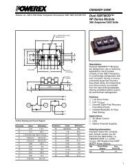
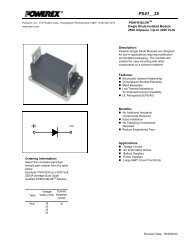
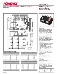
<strong>PM50CLA120</strong><br />
Intellimod L-<strong>Series</strong><br />
Three Phase IGBT Inverter<br />
50 Amperes/1200 Volts<br />
Electrical and Mechanical Characteristics, T j = 25°C unless otherwise specified<br />
Characteristics Symbol Test Conditions Min. Typ. Max. Units<br />
Control Sector<br />
Short Circuit Trip Level SC -20°C ≤ T j ≤ 125°C, V D = 15V 100 — — Amperes<br />
Short Circuit Current Delay Time t off(SC) V D = 15V — 0.2 — µs<br />
Over Temperature Protection OT Trip Level 135 145 155 °C<br />
(Detect T j of IGBT Chip) OT R Reset Level — 125 — °C<br />
Supply Circuit Under-voltage Protection UV Trip Level 11.5 12.0 12.5 Volts<br />
(-20 ≤ T j ≤ 125°C) UV R Reset Level — 12.5 — Volts<br />
Circuit Current I D V D = 15V, V CIN = 15V, V N1 -V NC — 15 25 mA<br />
V D = 15V, V CIN = 15V, V XP1 -V XPC — 5 10 mA<br />
Input ON Threshold Voltage V th(on) Applied between U P -V UPC , 1.2 1.5 1.8 Volts<br />
Input OFF Threshold Voltage V th(off) V P -V VPC , W P -V WPC , U N - V N - W N -V NC 1.7 2.0 2.3 Volts<br />
Fault Output Current* I FO(H) V D = 15V, V CIN = 15V — — 0.01 mA<br />
I FO(L) V D = 15V, V CIN = 15V — 10 15 mA<br />
Fault Output Pulse Width* t FO V D = 15V 1.0 1.8 — ms<br />
*Fault output is given only when the internal SC, OT and UV protections schemes of either upper or lower devide operate to protect it.<br />
Thermal Characteristics<br />
Characteristic Symbol Condition Min. Typ. Max. Units<br />
Junction to Case Thermal Resistance R th(j-c)Q IGBT (Per 1/6 Module) — — 0.26 °C/Watt<br />
R th(j-c)D FWDi (Per 1/6 Module) — — 0.39 °C/Watt<br />
Contact Thermal Resistance R th(c-f) Case to Fin Per Module, — — 0.038 °C/Watt<br />
Thermal Grease Applied<br />
Recommended Conditions for Use<br />
Characteristic Symbol Condition Value Units<br />
Supply Voltage V CC Applied across P-N Terminals ≤800 Volts<br />
Control Supply Voltage** V D Applied between V UP1 -V UPC , 15.0 ± 1.5 Volts<br />
V VP1 -V VPC , V WP1 -V WPC , V N1 -V NC<br />
Input ON Voltage V CIN(on) Applied between U P -V UPC , ≤0.8 Volts<br />
Input OFF Voltage V CIN(off) V P -V VPC , W P -V WPC , U N - V N - W N -V NC ≥9.0 Volts<br />
PWM Input Frequency f PWM — ≤20 kHz<br />
Arm Shoot-through Blocking Time t DEAD Input Signal ≥2.5 µs<br />
** With ripple satisfying the following conditions: dv/dt swing ≤ ±5V/µs, Variation ≤ 2V peak to peak.<br />
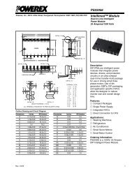
T C Measurement Point<br />
Arm UP VP WP UN VN WN<br />
Y<br />
BOTTOM VIEW<br />
Axis IGBT FWDi IGBT FWDi IGBT FWDi IGBT FWDi IGBT FWDi IGBT FWDi<br />
X<br />
X 28.3 28.4 65.0 64.9 86.9 86.9 39.3 39.2 54.0 54.1 76.0 76.1<br />
Y -7.7 1.5 -7.7 1.5 -7.7 1.5 5.7 -3.5 5.7 -3.5 5.7 -3.5<br />
3