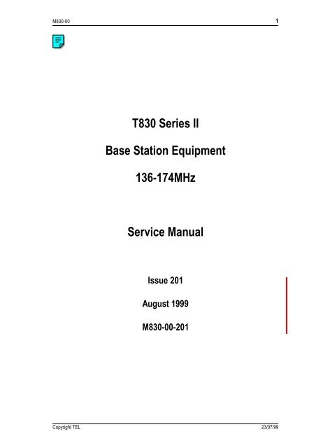
T830 Series II Base Station Equipment 136-174MHz Service Manual
T830 Series II Base Station Equipment 136-174MHz Service Manual
T830 Series II Base Station Equipment 136-174MHz Service Manual

You also want an ePaper? Increase the reach of your titles
YUMPU automatically turns print PDFs into web optimized ePapers that Google loves.
M830-00 1<br />
<strong>T830</strong> <strong>Series</strong> <strong>II</strong><br />
<strong>Base</strong> <strong>Station</strong> <strong>Equipment</strong><br />
<strong>136</strong>-<strong>174MHz</strong><br />
<strong>Service</strong> <strong>Manual</strong><br />
Issue 201<br />
August 1999<br />
M830-00-201<br />
Copyright TEL 23/07/99
2 M830-00<br />
T800<br />
Head Office<br />
New Zealand<br />
Tait Electronics Ltd<br />
558 Wairakei Road<br />
P.O. Box 1645<br />
Christchurch<br />
New Zealand<br />
Phone: 64 3 358-3399<br />
Fax: 64 3 358-3636<br />
Radio Systems Division<br />
535 Wairakei Road<br />
P.O. Box 1645<br />
Christchurch<br />
New Zealand<br />
Phone: 64 3 358-3399<br />
Fax: 64 3 358-2825<br />
Australia<br />
Tait Electronics (Aust) Pty Ltd<br />
186 Granite Street<br />
Geebung<br />
Queensland 4034<br />
P.O. Box 679<br />
Virginia<br />
Queensland 4014<br />
Australia<br />
Phone: 61 7 3865-7799<br />
Toll Free: 1800 077-112<br />
Fax: 61 7 3865-7990<br />
Beijing<br />
Tait Mobile Radio (HK) Ltd<br />
Beijing Representative Office<br />
Room 812, Tower A<br />
Beijing Bright China<br />
Chang An Building<br />
No. 7 Jianguomennei Dai Jei<br />
Dongcheng District<br />
Beijing<br />
China 100005<br />
Canada<br />
Tait Mobile Radio Inc.<br />
Unit 5, 158 Anderson Avenue<br />
Markham<br />
Ontario L6E1A9<br />
Canada<br />
Phone: 1 905 472-1100<br />
Toll Free: 1 800 890-8248<br />
Fax: 1 905 472-5300<br />
France<br />
Tait France Sarl<br />
2 Avenue de la Cristallerie<br />
92 316 Sèvres, Cedex<br />
France<br />
Phone: 33 1 41 14-05-50<br />
Fax: 33 1 41 14-05-55<br />
Germany<br />
Tait Mobilfunk GmbH<br />
Willstätterstraße 50<br />
D-90449 Nürnberg 60<br />
Germany<br />
Phone: 49 911 96 746-0<br />
Fax: 49 911 96 746-79<br />
Hong Kong<br />
Tait Mobile Radio (HK) Ltd<br />
Unit 2216, North Tower<br />
Concordia Plaza<br />
1, Science Museum Road<br />
Tsim Sha Tsui East<br />
Kowloon<br />
Phone: 852 2369-3040<br />
Fax: 852 2369-3009<br />
New Zealand<br />
Tait Communications Ltd<br />
Unit 4, 75 Blenheim Road<br />
P.O. Box 1185<br />
Christchurch<br />
Phone: 64 3 348-3301<br />
Fax: 64 3 343-0558<br />
Singapore<br />
Tait Electronics (Far East) Pte<br />
Ltd<br />
4 Leng Kee Road<br />
SIS Building #05-11A<br />
Singapore 159088<br />
Phone: 65 471-2688<br />
Fax: 65 479-7778<br />
Taiwan<br />
Tait Mobile (Taiwan) Ltd<br />
1104, No. 142 Chung Hsiao E. Rd<br />
Sec. 4<br />
Taipei<br />
Taiwan<br />
Phone: 886 2 2731-1290<br />
Fax: 886 2 2711-6351<br />
Thailand<br />
Tait Mobile Radio Ltd<br />
14/1 Suwan Tower<br />
Third Floor<br />
Soi Saladaeng 1<br />
North Sathorn Road<br />
Bangrak<br />
Bangkok 10500<br />
Thailand<br />
Phone: 662 267-6290<br />
Fax: 662 267-6293<br />
United Kingdom<br />
Tait Europe Ltd<br />
Ermine Business Park<br />
Ermine Road<br />
Huntingdon<br />
Cambridgeshire PE18 6YA<br />
United Kingdom<br />
Phone: 44 1480-52255<br />
Fax: 44 1480-411996<br />
USA<br />
Tait Electronics (USA) Inc.<br />
9434 Old Katy Road<br />
Suite 110<br />
Houston<br />
Texas 77055<br />
USA<br />
Phone: 1 713 984-8684<br />
Toll Free: 1 800 222-1255<br />
Fax: 1 713 468-6944<br />
Internet<br />
http://www.taitworld.com<br />
23/07/99 Copyright TEL
M830-00 3<br />
About This <strong>Manual</strong><br />
Scope<br />
This manual contains general, technical and servicing information<br />
on <strong>T830</strong> <strong>Series</strong> <strong>II</strong> 25W, 50W and 100W base stations which<br />
comprise the following equipment:<br />
25W base station<br />
50W base station<br />
100W base station<br />
T835 receiver<br />
T836 25W transmitter<br />
T835 receiver<br />
T837 exciter<br />
T838 50W power amplifier<br />
T835 receiver<br />
T837 exciter<br />
T839 100W power amplifier<br />
Format<br />
Revision Packages<br />
We have published this manual in a ring binder so that "revision<br />
packages" containing additional information pertaining to new<br />
issues of PCBs can be added as required.<br />
Revision packages will normally be published to coincide with<br />
the release of information on a new PCB, and may also contain<br />
additions or corrections pertaining to other parts of the manual.<br />
You may order as many packages as you require from your local<br />
Tait Dealer or Customer <strong>Service</strong> Organisation. Revision packages<br />
are supplied ready-punched for inclusion in your manual.<br />
Revision Control<br />
2<br />
Each page in this manual has a date of issue. This is to comply<br />
with various Quality Standards, but will also serve to identify<br />
which pages have been updated and when. Each page and its<br />
publication date is listed in the "List of Effective Pages", and a<br />
new list containing any new/revised pages and their publication<br />
dates will be sent with each revision package.<br />
Any portion of text that has been changed is marked by a vertical<br />
line (as shown at left) in the outer margin of the page or column.<br />
Where the removal of an entire paragraph means there is<br />
no text left to mark, an arrow (as shown at left) will appear in<br />
the outer margin. The number beside the arrow will indicate<br />
how many paragraphs have been deleted. Changes to diagrams<br />
that cannot be marked by these methods will be explained in an<br />
Amendments Box added to the diagram.<br />
The manual issue and revision status are indicated by the last<br />
three digits of the manual product code. These digits start at 200<br />
and will increment through 201, 202, 203, etc., as revision packages<br />
are published, e.g:<br />
issue status<br />
2 0 3<br />
revision status<br />
Copyright TEL 23/07/99
4 M830-00<br />
Thus, issue 203 indicates the third revision to issue 2 and means<br />
that three packages should have been added to the manual. The<br />
issue digit will only change if there is a major product revision,<br />
or if the number of revision packages to be included means that<br />
the manual becomes difficult to use, at which point a new issue<br />
manual will be published in a new ring binder.<br />
PCB Information<br />
Errors<br />
PCB information is provided for all current issue PCBs, as well<br />
as all previous issue PCBs manufactured in production quantities,<br />
and is grouped according to PCB. Thus, you will find the<br />
parts list, grid reference index (if necessary), PCB layouts and<br />
circuit diagram(s) for each individual PCB grouped together.<br />
If you find an error in this manual, or have a suggestion on how<br />
it might be improved, please do not hesitate to contact Customer<br />
Support, Radio Systems Division, Tait Electronics Ltd, Christchurch,<br />
New Zealand (full contact details are on page 2).<br />
Updating <strong>Equipment</strong> And <strong>Manual</strong>s<br />
In the interests of improving performance, reliability or servicing, Tait Electronics Ltd<br />
reserve the right to update their equipment and/or manuals without prior notice.<br />
Copyright<br />
All information contained in this manual is the property of Tait Electronics Ltd. All<br />
rights are reserved. This manual may not, in whole or part, be copied, photocopied,<br />
reproduced, translated stored or reduced to any electronic medium or machine readable<br />
form without prior written permission from Tait Electronics Ltd.<br />
Ordering Tait <strong>Service</strong> <strong>Manual</strong>s<br />
You can order additional copies of this service manual from your nearest Tait Dealer or<br />
Customer <strong>Service</strong> Organisation. When ordering, make sure you quote the correct Tait<br />
product code ("M" number). Note that only the latest issue of the manual will be available<br />
for order.<br />
Publication Information<br />
<strong>T830</strong> <strong>Series</strong> <strong>II</strong> <strong>Service</strong> <strong>Manual</strong><br />
Issue Publication Date Product Code Incorporates Revision Package<br />
200<br />
201<br />
April 1998<br />
August 1999<br />
M830-00-200<br />
M830-00-201<br />
—<br />
R830-00-201<br />
23/07/99 Copyright TEL
M830-00 5<br />
Table Of Contents<br />
This manual is divided into nine parts as listed below, with each part being further subdivided<br />
into sections. There is a detailed table of contents at the start of each part and/<br />
or section.<br />
Part<br />
Title<br />
A<br />
B<br />
C<br />
D<br />
E<br />
F<br />
G<br />
H<br />
I<br />
Introduction To Servicing<br />
T835 Receiver<br />
T836 Transmitter & T837 Exciter<br />
T838 & T839 Power Amplifiers<br />
<strong>T830</strong> VCO PCB Information<br />
Installation<br />
System Configurations<br />
T800 Ancillary <strong>Equipment</strong><br />
Using T800 <strong>Series</strong> <strong>II</strong> <strong>Equipment</strong> In A <strong>Series</strong> I Rack Frame<br />
Copyright TEL 30/04/98
6 M830-00<br />
List Of Effective Pages<br />
The total number of pages in this <strong>Manual</strong> is 444, as listed below.<br />
Page Issue Date Page Issue Date<br />
1 23/07/99<br />
2 23/07/99<br />
3 23/07/99<br />
4 23/07/99<br />
5 30/04/98<br />
6 23/07/99<br />
7 23/07/99<br />
8 23/07/99<br />
9 23/07/99<br />
10 23/07/99<br />
11 23/07/99<br />
12 23/07/99 (blank)<br />
Part A<br />
I 23/07/99<br />
<strong>II</strong> 30/04/98 (blank)<br />
1.1 23/07/99<br />
1.2 30/04/98<br />
2.1 30/04/98<br />
2.2 30/04/98<br />
2.3 23/07/99<br />
2.4 23/07/99<br />
3.1 30/04/98<br />
3.2 23/07/99<br />
4.1 30/04/98<br />
4.2 30/04/98<br />
Part B<br />
I 30/04/98<br />
<strong>II</strong> 30/04/98 (blank)<br />
1.1 23/07/99<br />
1.2 30/04/98 (blank)<br />
1.3 30/04/98 (fold-out)<br />
1.4 30/04/98 (fold-out)<br />
1.5 23/07/99<br />
1.6 23/07/99<br />
1.7 23/07/99<br />
1.8 23/07/99<br />
1.9 23/07/99<br />
1.10 23/07/99<br />
1.11 23/07/99<br />
1.12 23/07/99<br />
1.13 23/07/99<br />
1.14 30/04/98 (blank)<br />
2.1 30/04/98<br />
2.2 30/04/98 (blank)<br />
2.3 30/04/98<br />
2.4 23/07/99<br />
2.5 30/04/98<br />
2.6 30/04/98<br />
2.7 30/04/98<br />
2.8 23/07/99<br />
2.9 23/07/99<br />
2.10 23/07/99<br />
2.11 23/07/99<br />
2.12 30/04/98 (blank)<br />
3.1 23/07/99<br />
3.2 23/07/99<br />
3.3 23/07/99<br />
3.4 30/04/98<br />
3.5 23/07/99<br />
3.6 23/07/99<br />
3.7 23/07/99<br />
3.8 23/07/99<br />
3.9 30/04/98<br />
3.10 23/07/99<br />
3.11 23/07/99<br />
3.12 23/07/99<br />
3.13 23/07/99<br />
3.14 23/07/99<br />
4.1 23/07/99<br />
4.2 23/07/99<br />
4.3 23/07/99<br />
4.4 23/07/99<br />
4.5 30/04/98<br />
4.6 23/07/99<br />
4.7 23/07/99<br />
4.8 23/07/99<br />
4.9 30/04/98 (fold-out)<br />
4.10 30/04/98 (fold-out) (blank)<br />
23/07/99 Copyright TEL
M830-00 7<br />
Page Issue Date Page Issue Date<br />
5.1 23/07/99<br />
5.2 23/07/99<br />
5.3 30/04/98<br />
5.4 30/04/98<br />
5.5 30/04/98<br />
5.6 23/07/99<br />
5.7 23/07/99<br />
5.8 30/04/98<br />
5.9 30/04/98<br />
5.10 30/04/98<br />
5.11 30/04/98<br />
5.12 23/07/99<br />
5.13 30/04/98<br />
5.14 30/04/98<br />
5.15 30/04/98<br />
5.16 23/07/99<br />
5.17 23/07/99<br />
5.18 30/04/98<br />
5.19 23/07/99<br />
5.20 30/04/98 (blank)<br />
6.1.1 23/07/99<br />
6.1.2 30/04/98 (blank)<br />
6.1.3 30/04/98<br />
6.1.4 30/04/98<br />
6.1.5 30/04/98<br />
6.1.6 30/04/98<br />
6.2.1 30/04/98<br />
6.2.2 30/04/98 (blank)<br />
6.2.3 23/07/99<br />
6.2.4 30/04/98<br />
6.2.5 30/04/98<br />
6.2.6 30/04/98<br />
6.2.7 30/04/98<br />
6.2.8 30/04/98<br />
6.2.9 30/04/98 (fold-out)<br />
6.2.10 30/04/98 (fold-out) (blank)<br />
6.2.11 30/04/98<br />
6.2.12 30/04/98<br />
6.2.13 30/04/98<br />
6.2.14 30/04/98 (blank)<br />
6.2.15 30/04/98 (fold-out)<br />
6.2.16 30/04/98 (fold-out)<br />
6.2.17 30/04/98 (fold-out)<br />
6.2.18 30/04/98 (fold-out)<br />
6.2.19 30/04/98 (fold-out)<br />
6.2.20 30/04/98 (fold-out)<br />
6.2.21 30/04/98 (fold-out)<br />
6.2.22 30/04/98 (fold-out)<br />
6.2.23 30/04/98 (fold-out)<br />
6.2.24 30/04/98 (fold-out)<br />
6.2.25 30/04/98 (fold-out)<br />
6.2.26 23/07/99 (fold-out)<br />
6.2.27 30/04/98 (fold-out)<br />
6.2.28 30/04/98 (fold-out) (blank)<br />
Part C<br />
I 30/04/98<br />
<strong>II</strong> 30/04/98 (blank)<br />
1.1 30/04/98<br />
1.2 30/04/98 (blank)<br />
1.3 30/04/98 (fold-out)<br />
1.4 30/04/98 (fold-out)<br />
1.5 30/04/98 (fold-out)<br />
1.6 30/04/98 (fold-out)<br />
1.7 23/07/99<br />
1.8 23/07/99<br />
1.9 23/07/99<br />
1.10 23/07/99<br />
1.11 23/07/99<br />
1.12 30/04/98<br />
1.13 23/07/99<br />
1.14 23/07/99<br />
1.15 23/07/99<br />
1.16 30/04/98 (blank)<br />
2.1 30/04/98<br />
2.2 30/04/98<br />
2.3 30/04/98<br />
2.4 23/07/99<br />
2.5 30/04/98<br />
2.6 23/07/99<br />
2.7 30/04/98<br />
2.8 23/07/99<br />
2.9 23/07/99<br />
2.10 23/07/99<br />
2.11 23/07/99<br />
2.12 30/04/98<br />
2.13 30/04/98<br />
2.14 30/04/98 (blank)<br />
3.1 23/07/99<br />
3.2 23/07/99<br />
3.3 23/07/99<br />
3.4 23/07/99<br />
3.5 30/04/98<br />
3.6 23/07/99<br />
3.7 23/07/99<br />
3.8 30/04/98<br />
3.9 23/07/99<br />
Copyright TEL 23/07/99
8 M830-00<br />
Page Issue Date Page Issue Date<br />
3.10 30/04/98<br />
3.11 23/07/99<br />
3.12 23/07/99<br />
3.13 23/07/99<br />
3.14 23/07/99<br />
4.1 23/07/99<br />
4.2 23/07/99<br />
4.3 23/07/99<br />
4.4 23/07/99<br />
4.5 23/07/99<br />
4.6 30/04/98<br />
4.7 23/07/99<br />
4.8 30/04/98<br />
4.9 30/04/98 (fold-out)<br />
4.10 30/04/98 (fold-out) (blank)<br />
4.11 30/04/98 (fold-out)<br />
4.12 30/04/98 (fold-out) (blank)<br />
5.1 23/07/99<br />
5.2 30/04/98<br />
5.3 30/04/98<br />
5.4 30/04/98<br />
5.5 30/04/98<br />
5.6 30/04/98<br />
5.7 30/04/98<br />
5.8 30/04/98<br />
5.9 30/04/98<br />
5.10 30/04/98<br />
5.11 23/07/99<br />
5.12 23/07/99<br />
5.13 30/04/98<br />
5.14 30/04/98<br />
5.15 30/04/98<br />
5.16 23/07/99<br />
5.17 30/04/98<br />
5.18 30/04/98<br />
5.19 23/07/99<br />
5.20 23/07/99<br />
6.1.1 23/07/99<br />
6.1.2 30/04/98 (blank)<br />
6.1.3 30/04/98<br />
6.1.4 30/04/98<br />
6.1.5 30/04/98<br />
6.1.6 30/04/98<br />
6.2.1 30/04/98<br />
6.2.2 30/04/98 (blank)<br />
6.2.3 23/07/99<br />
6.2.4 30/04/98<br />
6.2.5 30/04/98<br />
6.2.6 30/04/98<br />
6.2.7 30/04/98<br />
6.2.8 30/04/98<br />
6.2.9 30/04/98 (fold-out)<br />
6.2.10 30/04/98 (fold-out) (blank)<br />
6.2.11 30/04/98<br />
6.2.12 30/04/98<br />
6.2.13 30/04/98<br />
6.2.14 30/04/98 (blank)<br />
6.2.15 30/04/98 (fold-out)<br />
6.2.16 30/04/98 (fold-out)<br />
6.2.17 30/04/98 (fold-out)<br />
6.2.18 30/04/98 (fold-out)<br />
6.2.19 30/04/98 (fold-out)<br />
6.2.20 30/04/98 (fold-out)<br />
6.2.21 30/04/98 (fold-out)<br />
6.2.22 30/04/98 (fold-out)<br />
6.2.23 30/04/98 (fold-out)<br />
6.2.24 30/04/98 (fold-out)<br />
6.2.25 23/07/99 (fold-out)<br />
6.2.26 30/04/98 (fold-out)<br />
6.3.1 30/04/98<br />
6.3.2 30/04/98 (blank)<br />
6.3.3 23/07/99<br />
6.3.4 30/04/98<br />
6.3.5 30/04/98<br />
6.3.6 30/04/98<br />
6.3.7 30/04/98<br />
6.3.8 30/04/98<br />
6.3.9 30/04/98 (fold-out)<br />
6.3.10 30/04/98 (fold-out) (blank)<br />
6.3.11 30/04/98<br />
6.3.12 30/04/98<br />
6.3.13 30/04/98<br />
6.3.14 30/04/98 (blank)<br />
6.3.15 30/04/98 (fold-out)<br />
6.3.16 30/04/98 (fold-out)<br />
6.3.17 30/04/98 (fold-out)<br />
6.3.18 30/04/98 (fold-out)<br />
6.3.19 30/04/98 (fold-out)<br />
6.3.20 30/04/98 (fold-out)<br />
6.3.21 30/04/98 (fold-out)<br />
6.3.22 30/04/98 (fold-out)<br />
6.3.23 30/04/98 (fold-out)<br />
6.3.24 30/04/98 (fold-out)<br />
6.3.25 23/07/99 (fold-out)<br />
6.3.26 30/04/98 (fold-out)<br />
6.3.27 23/07/99<br />
6.3.28 23/07/99<br />
6.3.29 23/07/99<br />
6.3.30 23/07/99<br />
23/07/99 Copyright TEL
M830-00 9<br />
Page Issue Date Page Issue Date<br />
6.3.31 23/07/99<br />
6.3.32 23/07/99<br />
6.3.33 23/07/99 (fold-out)<br />
6.3.34 23/07/99 (fold-out) (blank)<br />
6.3.35 23/07/99<br />
6.3.36 23/07/99<br />
6.3.37 23/07/99<br />
6.3.38 23/07/99 (blank)<br />
6.3.39 23/07/99 (fold-out)<br />
6.3.40 23/07/99 (fold-out)<br />
6.3.41 23/07/99 (fold-out)<br />
6.3.42 23/07/99 (fold-out)<br />
6.3.43 23/07/99 (fold-out)<br />
6.3.44 23/07/99 (fold-out)<br />
6.3.45 23/07/99 (fold-out)<br />
6.3.46 23/07/99 (fold-out)<br />
6.3.47 23/07/99 (fold-out)<br />
6.3.48 23/07/99 (fold-out)<br />
6.3.49 23/07/99 (fold-out)<br />
6.3.50 23/07/99 (fold-out)<br />
Part D<br />
I 23/07/99<br />
<strong>II</strong> 30/04/98 (blank)<br />
1.1 30/04/98<br />
1.2 30/04/98 (blank)<br />
1.3 30/04/98 (fold-out)<br />
1.4 30/04/98 (fold-out)<br />
1.5 30/04/98<br />
1.6 23/07/99<br />
1.7 23/07/99<br />
1.8 30/04/98<br />
1.9 23/07/99<br />
1.10 23/07/99<br />
2.1 23/07/99<br />
2.2 30/04/98 (blank)<br />
2.3 23/07/99<br />
2.4 30/04/98<br />
2.5 23/07/99<br />
2.6 30/04/98<br />
2.7 23/07/99<br />
2.8 23/07/99<br />
3.1 23/07/99<br />
3.2 30/04/98 (blank)<br />
3.3 30/04/98<br />
3.4 30/04/98<br />
3.5 30/04/98<br />
3.6 30/04/98<br />
3.7 30/04/98<br />
3.8 30/04/98 (blank)<br />
3.9 30/04/98 (fold-out)<br />
3.10 30/04/98 (fold-out) (blank)<br />
4.1 23/07/99<br />
4.2 30/04/98 (blank)<br />
4.3 30/04/98<br />
4.4 30/04/98 (blank)<br />
4.5 30/04/98 (fold-out)<br />
4.6 30/04/98 (fold-out)<br />
4.7 30/04/98<br />
4.8 30/04/98<br />
4.9 30/04/98<br />
4.10 30/04/98<br />
4.11 23/07/99<br />
4.12 30/04/98<br />
4.13 23/07/99<br />
4.14 30/04/98 (blank)<br />
5.1.1 23/07/99<br />
5.1.2 30/04/98 (blank)<br />
5.1.3 23/07/99<br />
5.1.4 30/04/98<br />
5.1.5 30/04/98<br />
5.1.6 30/04/98<br />
5.2.1 30/04/98<br />
5.2.2 30/04/98 (blank)<br />
5.2.3 23/07/99<br />
5.2.4 30/04/98<br />
5.2.5 30/04/98<br />
5.2.6 30/04/98<br />
5.2.7 30/04/98 (fold-out)<br />
5.2.8 30/04/98 (fold-out) (blank)<br />
5.2.9 30/04/98<br />
5.2.10 30/04/98<br />
5.2.11 30/04/98 (fold-out)<br />
5.2.12 23/07/99 (fold-out)<br />
5.2.13 30/04/98 (fold-out)<br />
5.2.14 30/04/98 (fold-out)<br />
5.3.1 30/04/98<br />
5.3.2 30/04/98 (blank)<br />
5.3.3 23/07/99<br />
5.3.4 30/04/98<br />
5.3.5 30/04/98<br />
5.3.6 30/04/98<br />
5.3.7 30/04/98 (fold-out)<br />
5.3.8 30/04/98 (fold-out) (blank)<br />
5.3.9 30/04/98<br />
Copyright TEL 23/07/99
10 M830-00<br />
Page Issue Date Page Issue Date<br />
5.3.10 30/04/98<br />
5.3.11 30/04/98 (fold-out)<br />
5.3.12 23/07/99 (fold-out)<br />
5.3.13 30/04/98 (fold-out)<br />
5.3.14 30/04/98 (fold-out)<br />
Part E<br />
I 30/04/98<br />
<strong>II</strong> 30/04/98 (blank)<br />
1.1 30/04/98<br />
1.2 30/04/98<br />
1.3 30/04/98<br />
1.4 30/04/98 (blank)<br />
2.1 30/04/98<br />
2.2 30/04/98 (blank)<br />
2.3 23/07/99<br />
2.4 30/04/98<br />
2.5 30/04/98<br />
2.6 30/04/98<br />
2.7 30/04/98<br />
2.8 30/04/98<br />
2.9 30/04/98 (fold-out)<br />
2.10 30/04/98 (fold-out) (blank)<br />
Part F<br />
I 23/07/99<br />
<strong>II</strong> 23/07/99<br />
1.1 23/07/99 (fold-out)<br />
1.2 23/07/99 (fold-out)<br />
2.1 23/07/99 (fold-out)<br />
2.2 23/07/99 (fold-out)<br />
3.1 23/07/99 (fold-out)<br />
3.2 23/07/99 (fold-out)<br />
4.1 23/07/99<br />
4.2 23/07/99<br />
Part G<br />
I 30/04/98<br />
<strong>II</strong> 30/04/98<br />
1.1 23/07/99<br />
1.2 30/04/98<br />
1.3 30/04/98<br />
1.4 30/04/98 (blank)<br />
2.1 30/04/98<br />
2.2 30/04/98<br />
2.3 30/04/98<br />
2.4 30/04/98 (blank)<br />
3.1 30/04/98<br />
3.2 30/04/98 (blank)<br />
4.1 30/04/98<br />
4.2 30/04/98<br />
5.1 30/04/98<br />
5.2 30/04/98<br />
Part H<br />
I 23/07/99<br />
<strong>II</strong> 30/04/98 (blank)<br />
1 23/07/99<br />
2 30/04/98<br />
3 23/07/99<br />
4 30/04/98<br />
5 23/07/99<br />
6 23/07/99<br />
7 23/07/99<br />
8 23/07/99<br />
9 23/07/99<br />
10 23/07/99<br />
11 23/07/99<br />
12 23/07/99<br />
13 23/07/99<br />
14 23/07/99<br />
Part I<br />
I 30/04/98<br />
<strong>II</strong> 30/04/98 (blank)<br />
1.1 30/04/98<br />
1.2 30/04/98 (blank)<br />
2.1 23/07/99<br />
2.2 30/04/98<br />
2.3 30/04/98<br />
23/07/99 Copyright TEL
M830-00 11<br />
Page Issue Date Page Issue Date<br />
2.4 30/04/98<br />
2.5 23/07/99<br />
2.6 30/04/98<br />
2.7 30/04/98<br />
2.8 30/04/98 (blank)<br />
3.1 23/07/99<br />
3.2 30/04/98<br />
3.3 30/04/98<br />
3.4 30/04/98<br />
3.5 30/04/98<br />
3.6 30/04/98 (blank)<br />
Copyright TEL 23/07/99
12 M830-00<br />
23/07/99 Copyright TEL
M830-00 AI<br />
Part A<br />
Introduction To Servicing<br />
This part of the manual is divided into the sections listed below. These sections provide<br />
some general and advisory information on servicing procedures, and a brief history of<br />
PGM800Win programming software.<br />
Section Title Page<br />
1<br />
2<br />
3<br />
4<br />
1.1<br />
1.2<br />
1.3<br />
1.4<br />
2.1<br />
2.2<br />
2.3<br />
2.3.1<br />
2.3.2<br />
2.4<br />
2.5<br />
3.1<br />
3.1.1<br />
3.1.2<br />
3.2<br />
3.3<br />
4.1<br />
4.2<br />
General<br />
Additional Technical Information<br />
Caution: CMOS Devices<br />
Caution: Aerial Load<br />
Caution: Beryllium Oxide & Power Transistors<br />
Mechanical<br />
Torx Recess Head Screws<br />
Pozidriv & Philips Recess Head Screws<br />
Disassembly/Reassembly<br />
Receivers/Exciters/Transmitters<br />
Power Amplifiers<br />
Cover Screw Torques<br />
Chassis & Cover Compatibility<br />
Component Replacement<br />
Leaded Components<br />
Desoldering Iron Method<br />
Component Cutting Method<br />
Surface Mount Devices<br />
Cased Mica Capacitors<br />
Software History<br />
PGM800Win V1.0<br />
PGM800Win V2.00<br />
1.1<br />
1.1<br />
1.1<br />
1.2<br />
1.2<br />
2.1<br />
2.1<br />
2.2<br />
2.3<br />
2.3<br />
2.3<br />
2.3<br />
2.4<br />
3.1<br />
3.1<br />
3.1<br />
3.1<br />
3.2<br />
3.2<br />
4.1<br />
4.1<br />
4.1<br />
Figure Title Page<br />
1.1<br />
1.2<br />
2.1<br />
2.2<br />
2.3<br />
Typical Product Code & Serial Number Labels<br />
Typical Anti-static Bench Set-up<br />
Torx Screw Identification<br />
Pozidriv & Philips Screw & Screwdriver Identification<br />
Identification Of New-Design Chassis & Covers<br />
1.1<br />
1.2<br />
2.1<br />
2.2<br />
2.4<br />
Copyright TEL 23/07/99
A<strong>II</strong> M830-00<br />
30/04/98 Copyright TEL
M830-00 General A1.1<br />
1 General<br />
1.1 Additional Technical Information<br />
If you have any questions about this manual or the equipment it describes, please contact<br />
your nearest Tait Dealer or Customer <strong>Service</strong> Organisation. If necessary, you can get<br />
additional technical help from Customer Support, Radio Systems Division, Tait Electronics<br />
Ltd, Christchurch, New Zealand (full contact details are on page 2).<br />
When requesting information, please quote either the manual product code (e.g.<br />
M830-00-200), or the equipment product code and serial number which are printed on a<br />
label on the back of the product (as shown in Figure 1.1).<br />
this area used for regional<br />
Type Approval information<br />
T838-10-0000<br />
Rev 1<br />
900000<br />
Tait Electronics Limited<br />
Made in New Zealand<br />
product code<br />
serial number<br />
T835-10-0000 Rev 1<br />
900000<br />
Tait Electronics Limited<br />
Made in New Zealand<br />
Figure 1.1 Typical Product Code & Serial Number Labels<br />
If you require information about a particular PCB, please quote the full PCB internal<br />
part number (IPN) which is screen printed onto the top side of the board (refer to the<br />
appropriate PCB Information section in this manual for more details).<br />
1.2 Caution: CMOS Devices<br />
This equipment contains CMOS Devices which are susceptible to damage from static<br />
charges. Care when handling these devices is essential. For correct handling procedures<br />
refer to the manufacturers' data books, e.g. Philips data books covering CMOS<br />
devices, or Motorola CMOS data books, Section 5 'Handling', etc.<br />
An anti-static bench kit (refer to Figure 1.2) is available from Tait Electronics Ltd under<br />
the following product codes:<br />
• KS0001 - 1 conductive rubber bench mat<br />
- 1 earth lead to connect the mat to ground<br />
• KS0004 - 1 wrist strap.<br />
Copyright TEL 23/07/99
A1.2 General M830-00<br />
conductive<br />
wrist strap<br />
conductive rubber<br />
bench mat<br />
to building earth<br />
(not mains earth)<br />
Figure 1.2 Typical Anti-static Bench Set-up<br />
1.3 Caution: Aerial Load<br />
The equipment has been designed to operate safely under a wide range of aerial loading<br />
conditions. However, we strongly recommend that the transmitter should always be<br />
operated with a suitable load to prevent damage to the transmitter output power stage.<br />
1.4 Caution: Beryllium Oxide & Power Transistors<br />
The RF power transistors in current use all contain some beryllium oxide. This substance,<br />
while perfectly harmless in its normal solid form, can become a severe health<br />
hazard when it has been reduced to dust. For this reason the RF power transistors<br />
should not be broken open, mutilated, filed, machined, or physically damaged in any<br />
way that can produce dust particles.<br />
30/04/98 Copyright TEL
M830-00 Mechanical A2.1<br />
2 Mechanical<br />
2.1 Torx Recess Head Screws<br />
Torx recess head screws are becoming the standard screw head type in all T800 <strong>Series</strong> <strong>II</strong><br />
equipment, with Pozidriv and Philips recess head screws being used in fewer applications.<br />
The Torx recess head has the advantage of improved screwdriver tip location, reducing<br />
the chances of screw head damage caused by the driver tip rotating within the recess. In<br />
addition, using a ball-tip Torx screwdriver allows you to drive a Torx head screw with<br />
the driver on a slight angle, which can be useful in situations where access is restricted.<br />
It is important that you use the correct Torx screwdriver tip:<br />
M3 screws - T10<br />
M4 screws - T20.<br />
Figure 2.1 below shows a typical Torx recess head screw (actual hardware may differ<br />
slightly from this illustration due to variations in manufacturing techniques).<br />
"star" shaped recess with<br />
six internal notches<br />
Figure 2.1 Torx Screw Identification<br />
Copyright TEL 30/04/98
A2.2 Mechanical M830-00<br />
2.2 Pozidriv & Philips Recess Head Screws<br />
Pozidriv and Philips recess head screws will continue to be used in T800 <strong>Series</strong> <strong>II</strong> equipment<br />
in a few special applications. It is important that you use the correct type and size<br />
screwdriver for each screw type to avoid damaging the screw head.<br />
It is particularly important that you do not use Philips screwdrivers on Pozidriv screw<br />
heads as the tapered driving flutes of the Philips screwdriver do not engage correctly<br />
with the parallel-sided slots in the Pozidriv screw head. This can result in considerable<br />
damage to the screw head if the screwdriver tip turns inside the recess.<br />
Note:<br />
If you find you need excessive downwards pressure to keep the screwdriver<br />
tip in the Pozidriv screw head, you are probably using the wrong type and/<br />
or size screwdriver.<br />
Figure 2.2 below shows the main differences between typical Pozidriv and Philips screw<br />
heads and screwdriver tips (actual hardware may differ slightly from these illustrations<br />
due to variations in manufacturing techniques).<br />
Pozidriv<br />
Philips<br />
internal notches<br />
no special markings<br />
"star" markings<br />
between slots<br />
slots with parallel sides<br />
slots with tapered sides<br />
driving flutes with<br />
parallel sides<br />
driving flutes with<br />
tapered sides<br />
ridges between<br />
driving flutes<br />
Figure 2.2 Pozidriv & Philips Screw & Screwdriver Identification<br />
30/04/98 Copyright TEL
M830-00 Mechanical A2.3<br />
2.3 Disassembly/Reassembly<br />
2.3.1 Receivers/Exciters/Transmitters<br />
To carry out alignment or change option links, you need to remove only the top cover,<br />
i.e. the one adjacent to the front panel handle and on the opposite side to the main<br />
D-range connector (D-range 1/PL100).<br />
You need to remove the bottom cover to:<br />
• access transmitter RF power transistors and many SMD components<br />
• change solder blob links<br />
• fit test leads to circuit block access points.<br />
2.3.2 Power Amplifiers<br />
You should carry out the tuning and power output level setting procedures with the<br />
cover on.<br />
2.4 Cover Screw Torques<br />
Receivers/Exciters/Transmitters .. 1.36Nm/12in.lbf.<br />
Power Amplifiers .. 0.9Nm/in.lbf.<br />
Copyright TEL 23/07/99
A2.4 Mechanical M830-00<br />
2.5 Chassis & Cover Compatibility<br />
The chassis and covers used in T800 <strong>Series</strong> <strong>II</strong> modules incorporate a number of design<br />
changes to improve Electro-Magnetic Compatibility (EMC) performance. It is important<br />
that only the new-design covers are fitted to the new chassis to ensure correct<br />
mechanical fit and continued compliance with appropriate EMC Type Approval regulations.<br />
Figure 2.3 below shows some of the main features which can be used to identify the<br />
new-design chassis and covers.<br />
Chassis<br />
←Top View<br />
Rear View→<br />
4 holes in<br />
rear panel<br />
loom channel in<br />
top of walls<br />
groove in top<br />
of rear wall<br />
Top Cover<br />
provision for mounting speaker<br />
(future development)<br />
ridge on top<br />
of rear wall<br />
Bottom Cover<br />
additional walls<br />
Figure 2.3 Identification Of New-Design Chassis & Covers<br />
23/07/99 Copyright TEL
M830-00 Component Replacement A3.1<br />
3 Component Replacement<br />
3.1 Leaded Components<br />
Whenever you are doing any work on the PCB that involves removing or fitting components,<br />
you must take care not to damage the copper tracks. The two satisfactory methods<br />
of removing components from plated-through hole (PTH) PCBs are detailed below.<br />
Note:<br />
The first method requires the use of a desoldering station, e.g. Philips SBC<br />
314 or Pace MBT-100E.<br />
3.1.1 Desoldering Iron Method<br />
Place the tip over the lead and, as the solder starts to melt, move the tip in a circular<br />
motion.<br />
Start the suction and continue the movement until 3 or 4 circles have been completed.<br />
Remove the tip while continuing suction to ensure that all solder is removed from<br />
the joint, then stop the suction.<br />
Before pulling the lead out, ensure it is not stuck to the plating.<br />
If the lead is still not free, resolder the joint and try again.<br />
Note:<br />
The desoldering iron does not usually have enough heat to desolder leads<br />
from the ground plane. Additional heat may be applied by holding a soldering<br />
iron on the tip of the desoldering iron (this may require some additional<br />
help).<br />
3.1.2 Component Cutting Method<br />
Cut the leads on the component side of the PCB.<br />
Heat the solder joint sufficiently to allow easy removal of the lead by drawing it<br />
out from the component side: do not use undue force.<br />
Fill the hole with solder and then clear with solderwick.<br />
Copyright TEL 30/04/98
A3.2 Component Replacement M830-00<br />
3.2 Surface Mount Devices<br />
Caution:<br />
Surface mount devices (SMDs) require special storage, handling,<br />
removal and replacement techniques. This equipment should be serviced<br />
only by an approved Tait Dealer or Customer <strong>Service</strong> Organisation<br />
equipped with the necessary facilities. Repairs attempted with<br />
incorrect equipment or by untrained personnel may result in permanent<br />
damage. If in doubt, contact your nearest Tait Dealer or Customer<br />
<strong>Service</strong> Organisation.<br />
3.3 Cased Mica Capacitors<br />
Cased mica capacitors can be removed by heating the top with a heavy-duty soldering<br />
iron and gently lifting the capacitor off the PCB with a solder-resistant spike or equivalent.<br />
23/07/99 Copyright TEL
M830-00 Software History A4.1<br />
4 Software History<br />
28/06/96 PGM800Win Version 1.0<br />
18/08/97 PGM800Win Version 2.00<br />
4.1 PGM800Win V1.0<br />
PGM800Win V1.0 is different in concept from DOS versions of PGM800 in that it is Windows<br />
1 based. It also includes many new and improved features over DOS versions of<br />
PGM800.<br />
The major changes are outlined below:<br />
• The Windows environment makes data entry and editing significantly easier.<br />
• PGM800Win includes several new radio models which are not programmable<br />
with DOS versions of PGM800.<br />
• Out of range frequencies will result in warning messages and will not be accepted<br />
for entry into the standard library module. User defined modules can be created,<br />
however, allowing variation from the standard library module.<br />
• Channel numbers default to 0-127 to match the EPROM memory locations. However,<br />
the user can change this setting so that the channel numbers run from 1-128<br />
to suit his/her particular needs.<br />
Note:<br />
The data files produced by BASEPROG V1.0 and all DOS versions of<br />
PGM800 are still compatible with PGM800Win V1.0.<br />
4.2 PGM800Win V2.00<br />
PGM800Win V2.00 is an upgraded and expanded version of PGM800Win V1.0. It has<br />
been developed specifically for T800 <strong>Series</strong> <strong>II</strong> base stations, but retains the ability to program<br />
<strong>Series</strong> I equipment.<br />
The major changes are outlined below:<br />
• PGM800Win V2.0 will program T800 <strong>Series</strong> <strong>II</strong> base station modules via serial communications.<br />
• Deviation and reference modulation settings are written automatically to the<br />
radio.<br />
1. Windows is a registered trademark of the Microsoft Corporation.<br />
Copyright TEL 30/04/98
A4.2 Software History M830-00<br />
• Extra information that is not stored in the radio (but which is still relevant to the<br />
radio) can be saved to a file on disk (e.g. note field, auxiliary pin names, etc.).<br />
Note:<br />
The data files produced by BASEPROG V1.0, all DOS versions of PGM800,<br />
and PGM800Win V1.0 are still compatible with PGM800Win V2.00.<br />
30/04/98 Copyright TEL
M830-00 BI<br />
Part B<br />
T835 Receiver<br />
This part of the manual is divided into six sections, as listed below. There is a detailed<br />
table of contents at the start of each section.<br />
Section<br />
Title<br />
1 General Information<br />
2 Circuit Operation<br />
3 Initial Tuning & Adjustment<br />
4 Functional Testing<br />
5 Fault Finding<br />
6 PCB Information<br />
Copyright TEL 30/04/98
B<strong>II</strong> M830-00<br />
30/04/98 Copyright TEL
M830-00 T835 General Information B1.1<br />
1 T835 General Information<br />
This section provides a brief description of the T835 receiver, along with detailed specifications<br />
and a list of types available.<br />
The following topics are covered in this section.<br />
Section Title Page<br />
1.1 Introduction 1.5<br />
1.2<br />
1.2.1<br />
1.2.2<br />
1.2.3<br />
1.2.4<br />
1.2.4.1<br />
1.2.4.2<br />
1.2.4.3<br />
1.2.5<br />
1.2.6<br />
1.2.6.1<br />
1.2.6.2<br />
1.2.6.3<br />
Specifications<br />
Introduction<br />
General<br />
RF Section<br />
Audio Section<br />
General<br />
CTCSS<br />
Mute Operation<br />
Microcontroller<br />
Test Standards<br />
European Telecommunication Standard (ETS)<br />
DTI CEPT Recommendation T/R-24-01<br />
Telecommunications Industry Association<br />
1.6<br />
1.6<br />
1.7<br />
1.7<br />
1.9<br />
1.9<br />
1.9<br />
1.10<br />
1.10<br />
1.10<br />
1.10<br />
1.11<br />
1.11<br />
1.3 Product Codes 1.12<br />
1.4 Standard Product Range 1.13<br />
Figure Title Page<br />
1.1<br />
1.2<br />
T835 Main Circuit Block Identification<br />
T835 Front Panel Controls<br />
1.4<br />
1.4<br />
Copyright TEL 23/07/99
B1.2 T835 General Information M830-00<br />
30/04/98 Copyright TEL
M830-00 T835 General Information B1.3<br />
replace A4 pages B1.3/B1.4 with A3 pages B1.3/B1.4<br />
Copyright TEL 30/04/98
B1.4 T835 General Information M830-00<br />
replace A4 pages B1.3/B1.4 with A3 pages B1.3/B1.4<br />
30/04/98 Copyright TEL
M830-00 T835 General Information B1.5<br />
1.1 Introduction<br />
The T835 is a high performance microprocessor controlled FM base station receiver<br />
designed for single or multichannel operation in the <strong>136</strong> to <strong>174MHz</strong> frequency range 1 .<br />
The receiver is a dual conversion superhet with a synthesised local oscillator. The first<br />
IF is 21.4MHz, allowing exceptionally high spurious signal rejection to be achieved in<br />
the receiver front end. The second IF section (455kHz) combines amplitude limiting,<br />
detection and RSSI within a single integrated circuit. This IC also drives a noise level<br />
detector for gating the audio output. RSSI can also be used to drive a carrier mute for<br />
audio output gating (link selectable).<br />
The audio section output can be adjusted to deliver >+10dBm to a 600 ohm balanced<br />
output, and 1W to a local monitor speaker. A flat or de-emphasised audio response is<br />
link selectable.<br />
The synthesiser frequency is programmed via the serial communications port. Eight<br />
channel select lines are accessible via an optional D-range connector (D-range 2 -<br />
T800-03-0000) at the rear of the set.<br />
All components except those on the VCO board are mounted on a single PCB. This is<br />
secured to a die-cast chassis which is divided into compartments to individually shield<br />
each section of circuitry. Access to both sides of the main PCB is obtained by removing<br />
each of the two chassis covers. There is provision within the chassis to mount small<br />
option PCBs.<br />
The front panel controls include gating sensitivity, line level, monitor volume and a<br />
monitor mute switch.<br />
The T835 has a width of 60mm and occupies a single space in a Tait rack frame, which<br />
has the ability to accommodate up to seven standard modules.<br />
1. Although capable of operating over the <strong>136</strong>-<strong>174MHz</strong> frequency range, the T835 has a<br />
3MHz switching range (see Section 1.2.3 and Section 3.1).<br />
Copyright TEL 23/07/99
B1.6 T835 General Information M830-00<br />
1.2 Specifications<br />
1.2.1 Introduction<br />
The performance figures given are minimum figures, unless otherwise indicated, for<br />
equipment tuned with the maximum switching range and operating at standard room<br />
temperature (+22°C to +28°C) and standard test voltage (13.8V DC).<br />
Where applicable, the test methods used to obtain the following performance figures are<br />
those described in the EIA and ETS specifications. However, there are several parameters<br />
for which performance according to the CEPT specification is given. Refer to Section<br />
1.2.6 for details of test standards.<br />
Details of test methods and the conditions which apply for Type Approval testing in all<br />
countries can be obtained from Tait Electronics Ltd.<br />
The terms "wide bandwidth", "mid bandwidth" and "narrow bandwidth" used in this<br />
and following sections are defined in the following table.<br />
Channel Spacing<br />
Modulation<br />
100% Deviation<br />
Receiver<br />
IF Bandwidth<br />
Wide Bandwidth 25kHz ±5.0kHz 15.0kHz<br />
Mid Bandwidth 20kHz ±4.0kHz 12.0kHz<br />
Narrow Bandwidth 12.5kHz ±2.5kHz 7.5kHz<br />
Sensitivity and distortion figures are stated for standard operating conditions which<br />
includes audio de-emphasis. Note that the sensitivity and distortion figures will be<br />
degraded when flat audio is selected.<br />
Link PL210<br />
Link PL220<br />
De-emphasised Audio 1-2 2-3<br />
Flat Audio 2-3 1-2<br />
23/07/99 Copyright TEL
M830-00 T835 General Information B1.7<br />
1.2.2 General<br />
Number Of Channels .. 128 (standard) 1<br />
Supply Voltage:<br />
Operating Voltage .. 10.8 to 16V DC<br />
Standard Test Voltage .. 13.8V DC<br />
Polarity .. negative earth only<br />
Polarity Protection .. crowbar diode<br />
Supply Current:<br />
Standby .. 350mA<br />
Full Audio .. 800mA<br />
Operating Temperature Range .. -30°C to +60°C<br />
Dimensions:<br />
Height .. 183mm<br />
Width .. 60mm<br />
Length .. 324mm<br />
Weight .. 2.13kg<br />
1.2.3 RF Section<br />
Frequency Range .. <strong>136</strong>-<strong>174MHz</strong><br />
Type .. dual conversion superheterodyne<br />
Frequency Increment .. 5 or 6.25kHz<br />
Switching Range .. 3MHz (i.e. ±1.5MHz from the centre<br />
frequency)<br />
Input Impedance .. 50 ohms<br />
Frequency Stability .. ±2.5ppm, -30°C to +60°C<br />
(see also Section 1.4)<br />
(±1ppm available for special<br />
applications)<br />
Signal Strength Indicator .. -115dBm to -70dBm, 3.5 to 6.5V<br />
(RSSI)<br />
at approx. 15dB/V<br />
1. Additional channels may be factory programmed. Contact your nearest Tait Dealer or<br />
Customer <strong>Service</strong> Organisation.<br />
Copyright TEL 23/07/99
B1.8 T835 General Information M830-00<br />
IF Amplifiers:<br />
Frequencies .. 21.4MHz and 455kHz<br />
Bandwidths-<br />
Narrow Bandwidth (NB) .. 7.5kHz<br />
Mid Bandwidth (MB) .. 12kHz<br />
Wide Bandwidth (WB) .. 15kHz<br />
Sensitivity (De-emphasised Response):<br />
Single Channel .. -117dBm<br />
Bandspread (12dB Sinad) .. -115dBm (across switching range)<br />
Sensitivity (Flat Response):<br />
Single Channel .. -111dBm<br />
Bandspread (12dB Sinad) .. -109dBm (across switching range)<br />
Signal+Noise To Noise Ratio (Typical):<br />
De-emphasised<br />
RF Level -107dBm (CEPT) .. 30dB (WB) 25dB (WB)<br />
25dB (NB) 20dB (NB)<br />
RF Level -83dBm (CEPT) .. 54dB (MB) 49dB (MB)<br />
50dB (NB) 45dB (NB)<br />
RF Level -57dBm (EIA) .. 55dB (WB) 52dB (WB)<br />
Selectivity:<br />
Narrow Bandwidth (±12.5kHz) .. 86dB minimum, 89dB typical<br />
Mid Bandwidth (±20kHz) .. 87dB minimum, 90dB typical<br />
Wide Bandwidth (±25kHz) .. 92dB minimum, 95dB typical<br />
Offset Selectivity (Canada only) .. 20dB<br />
Spurious Response Attenuation .. 100dB (typical)<br />
Intermodulation Response Attenuation:<br />
Narrow Bandwidth .. 80dB CEPT (typical)<br />
Mid Bandwidth .. 80dB CEPT (typical)<br />
Wide Bandwidth .. 85dB EIA (typical)<br />
Blocking .. 100dB<br />
Co-channel Rejection .. 6dB<br />
Amplitude Characteristic .. 3dB<br />
Spurious Emissions:<br />
Conducted .. -90dBm to 4GHz<br />
Radiated .. -57dBm to 1GHz<br />
-47dBm to 4GHz<br />
Flat<br />
23/07/99 Copyright TEL
M830-00 T835 General Information B1.9<br />
1.2.4 Audio Section<br />
1.2.4.1 General<br />
Outputs Available .. line and monitor<br />
Frequency Response .. flat or de-emphasised (750µs)<br />
(link selectable)<br />
Flat Response:<br />
Bandwidth .. 67 to 3400Hz<br />
Response .. within +1, -2dB of output level<br />
at 1kHz<br />
De-emphasised Response:<br />
Bandwidth .. 300 to 3400Hz<br />
Response .. within +1, -3dB of a 6dB/octave<br />
de-emphasis characteristic (ref. 1kHz)<br />
Line Output:<br />
Power .. adjustable to >+10dBm<br />
Load Impedance .. 600 ohms<br />
Distortion (@ -70dBm signal level):<br />
De-emphasised Flat<br />
Wide Bandwidth .. ≤2% ≤2%<br />
Mid & Narrow Bandwidth .. ≤2% ≤4%<br />
Monitor Output:<br />
Power .. 1W<br />
Speaker Impedance .. 4 ohms<br />
Distortion .. ≤3%<br />
(@ -70dBm signal level, links set to de-emphasis)<br />
1.2.4.2 CTCSS<br />
Linkable High Pass Filter:<br />
Bandwidth .. 350 to 3400Hz<br />
Response .. within +1, -3dB of level at 1kHz<br />
Hum And Noise .. 30dB min. at 250.3Hz<br />
(1kHz at 60% system deviation<br />
35dB typical (67 to 240Hz)<br />
CTCSS at 10% system deviation)<br />
Tone Detect:<br />
Tone Squelch Opening .. better than 6dB sinad<br />
3dB sinad at 250.3Hz (typical)<br />
4dB sinad at 100Hz (typical)<br />
Tone Detect Bandwidth .. ±2.1Hz accept (typical)<br />
±3.0Hz reject (typical)<br />
Response Time .. 150ms open and close (typical)<br />
Copyright TEL 23/07/99
B1.10 T835 General Information M830-00<br />
1.2.4.3 Mute Operation<br />
Systems Available .. noise mute and carrier mute<br />
Noise Mute:<br />
Operating Range .. 6-20dB sinad<br />
Hysteresis .. 1.5 to 6dB<br />
Threshold .. adjustable to -105dBm<br />
Opening Time .. 20ms<br />
Closing Time .. 50ms<br />
Carrier Mute (Optional):<br />
Operating Range .. -115 to -80dBm<br />
Hysteresis .. 2 to 10dB<br />
Opening Time .. 5ms<br />
Closing Time .. 50ms<br />
Note:<br />
The opening and closing times given above are for the standard set-up<br />
(SL210 linked and SL220 not linked - refer to Section 3.8).<br />
1.2.5 Microcontroller<br />
Auxiliary Ports:<br />
Open Drain Type .. capable of sinking 2.25mA via 2k2Ω<br />
V ds max. .. 5V<br />
1.2.6 Test Standards<br />
Where applicable, this equipment is tested in accordance with the following standards.<br />
1.2.6.1 European Telecommunication Standard<br />
ETS 300 086 January 1991<br />
Radio equipment and systems; land mobile service; technical characteristics and test<br />
conditions for radio equipment with an internal or external RF connector intended primarily<br />
for analogue speech.<br />
ETS 300 113 March 1996<br />
Radio equipment and systems; land mobile service; technical characteristics and test<br />
conditions for radio equipment intended for the transmission of data (and speech) and<br />
having an antenna connector.<br />
ETS 300 219 October 1993<br />
Radio equipment and systems; land mobile service; technical characteristics and test<br />
conditions for radio equipment transmitting signals to initiate a specific response in the<br />
receiver.<br />
23/07/99 Copyright TEL
M830-00 T835 General Information B1.11<br />
ETS 300 279 February 1996<br />
Radio equipment and systems; electromagnetic compatibility (EMC) standard for private<br />
land mobile radio (PMR) and ancillary equipment (speech and/or non-speech).<br />
1.2.6.2 DTI CEPT Recommendation T/R-24-01<br />
Annex I: 1988<br />
Technical characteristics and test conditions for radio equipment in the land mobile<br />
service intended primarily for analogue speech.<br />
Annex <strong>II</strong>: 1988<br />
Technical characteristics of radio equipment in the land mobile service with regard to<br />
quality and stability of transmission.<br />
1.2.6.3 Telecommunications Industry Association<br />
ANSI/TIA/EIA-603-1992<br />
Land mobile FM or PM communications equipment measurement and performance<br />
standards.<br />
Copyright TEL 23/07/99
B1.12 T835 General Information M830-00<br />
1.3 Product Codes<br />
The three groups of digits in the <strong>T830</strong> <strong>Series</strong> <strong>II</strong> product code provide information about<br />
the model, type and options fitted, according to the conventions described below.<br />
The following explanation of <strong>T830</strong> <strong>Series</strong> <strong>II</strong> product codes is not intended to suggest that<br />
any combination of features is necessarily available in any one product. Consult your<br />
nearest Tait Dealer or Customer <strong>Service</strong> Organisation for more information regarding<br />
the availability of specific models, types and options.<br />
Model<br />
The Model group indicates the basic function of the product, as follows:<br />
T83X-XX-XXXX<br />
T835 receiver<br />
T836 25W transmitter<br />
T837 exciter<br />
T838 50W power amplifier<br />
T839 100W power amplifier<br />
Type<br />
The Type group uses two digits to indicate the basic RF configuration of the product.<br />
The first digit in the Type group designates the frequency range:<br />
T83X-XX-XXXX ’1’ for <strong>136</strong>-156MHz<br />
’2’ for 148-<strong>174MHz</strong><br />
The second digit in the Type group indicates the channel spacing:<br />
T83X-XX-XXXX ’0’ for wide bandwidth (25kHz)<br />
’3’ for mid bandwidth (20kHz)<br />
’5’ for narrow bandwidth (12.5kHz)<br />
Options<br />
T83X-XX-XXXX<br />
The Options group uses four digits and/or letters to indicate<br />
any options that may be fitted to the product. This includes<br />
standard options and special options for specific customers.<br />
’0000’ indicates a standard Tait product with no options fitted.<br />
The large number of options precludes listing them here.<br />
23/07/99 Copyright TEL
M830-00 T835 General Information B1.13<br />
1.4 Standard Product Range<br />
The following table lists the range of standard T835 types (i.e. no options fitted) available<br />
at the time this manual was published. Consult your nearest Tait Dealer or Customer<br />
<strong>Service</strong> Organisation for more information.<br />
Frequency Range (MHz) a<br />
<strong>136</strong>-156<br />
IF Bandwidth (kHz) 7.5 12 15<br />
TCXO b<br />
±2.5ppm -30°C to +60°C • • •<br />
Receiver Type: T835- 15-0000 13-0000 10-0000<br />
Frequency Range (MHz) a 148-174<br />
IF Bandwidth (kHz) 7.5 12 15<br />
TCXO b ±2.5ppm -30°C to +60°C • • •<br />
Receiver Type: T835- 25-0000 23-0000 20-0000<br />
a. Selectable by solder links and the appropriate VCO - refer to Section<br />
3.7.<br />
b. A TCXO with a stability of ±1ppm (0°C to +60°C) is available to<br />
suit specific requirements. Contact your nearest authorised Tait<br />
Dealer or Customer <strong>Service</strong> Organisation for further details.<br />
You can identify the receiver type by checking the product code printed on a label on<br />
the rear of the chassis (Figure 1.1 in Part A shows typical labels). You can further verify<br />
the receiver type by checking the placement of an SMD resistor in the table that is screen<br />
printed onto the PCB (refer to Section 6.1 for more details).<br />
Copyright TEL 23/07/99
B1.14 T835 General Information M830-00<br />
30/04/98 Copyright TEL
M830-00 T835 Circuit Operation B2.1<br />
2 T835 Circuit Operation<br />
This section provides a basic description of the circuit operation of the T835 receiver.<br />
Note:<br />
Unless otherwise specified, the term "PGM800Win" used in this and following<br />
sections refers to version 2.00 and later of the software.<br />
Refer to Section 6 where the parts lists, grid reference index and diagrams will provide<br />
detailed information on identifying and locating components and test points on the<br />
main PCB. The parts list and diagrams for the VCO PCB are in Part E.<br />
The following topics are covered in this section.<br />
Section Title Page<br />
2.1 Introduction 2.3<br />
2.2 Receiver Front End 2.4<br />
2.3 Mixer 2.5<br />
2.4 IF Circuitry 2.5<br />
2.5 Noise Mute (Squelch) 2.6<br />
2.6 Carrier Mute 2.6<br />
2.7 Audio Processor 2.7<br />
2.8 Power Supply And Regulators 2.8<br />
2.9 Microcontroller 2.9<br />
2.10 Synthesised Local Oscillator 2.10<br />
2.11 VCO 2.11<br />
2.12 Received Signal Strength Indicator (RSSI) 2.11<br />
Figure Title Page<br />
2.1<br />
2.2<br />
2.3<br />
2.4<br />
2.5<br />
2.6<br />
T835 High Level Block Diagram<br />
T835 Front End, IF and Mute Block Diagram<br />
T835 Audio Processor Block Diagram<br />
T835 Power Supply And Regulator Block Diagram<br />
T835 Microcontroller Block Diagram<br />
T835 Synthesiser Block Diagram<br />
2.3<br />
2.4<br />
2.7<br />
2.8<br />
2.9<br />
2.10<br />
Copyright TEL 30/04/98
B2.2 T835 Circuit Operation M830-00<br />
30/04/98 Copyright TEL
M830-00 T835 Circuit Operation B2.3<br />
2.1 Introduction<br />
Noise<br />
Mute<br />
Front<br />
End<br />
Synthesised<br />
Local<br />
Oscillator<br />
Mixer Mixer Limiter<br />
21.4MHz<br />
IF<br />
Second<br />
Local<br />
Oscillator<br />
455kHz<br />
IF<br />
FM<br />
Detector<br />
Audio<br />
Processor<br />
Carrier<br />
Mute<br />
Speaker<br />
} 600Ω<br />
Line<br />
12.8MHz<br />
Master<br />
Oscillator<br />
RSSI<br />
Figure 2.1 T835 High Level Block Diagram<br />
The T835 receiver consists of a number of distinct stages:<br />
• front end<br />
• mixer<br />
• synthesised local oscillator<br />
• IF<br />
• audio processor<br />
• mute (squelch)<br />
• regulator circuits<br />
• received signal strength indicator (RSSI).<br />
These stages are clearly identifiable in Figure 2.1. Refer to the circuit diagrams in Section<br />
6 for further detail.<br />
Copyright TEL 30/04/98
B2.4 T835 Circuit Operation M830-00<br />
2.2 Receiver Front End<br />
(Refer to the front end, IF section and audio processor circuit diagrams (sheets 4, 3 and 2<br />
respectively) in Section 6.)<br />
Local Oscillator<br />
(From Synthesiser)<br />
RF In<br />
<strong>136</strong>-<strong>174MHz</strong><br />
Harmonic<br />
Filter<br />
Doublet<br />
Filter<br />
RF<br />
Amp<br />
Doublet<br />
Filter<br />
2dB Pad<br />
Diplexer<br />
Post<br />
Mixer<br />
Amp<br />
4-Pole<br />
Crystal<br />
Filter<br />
IF<br />
Amp<br />
Mixer<br />
21.4MHz<br />
2-Pole<br />
Crystal<br />
Filter<br />
21.4MHz<br />
Mixer<br />
(NE612)<br />
Ceramic<br />
Filter<br />
IF<br />
Amp<br />
455kHz<br />
Limiter<br />
(NE614)<br />
FM<br />
Detector<br />
(NE614)<br />
Low<br />
Pass<br />
Filter<br />
Audio<br />
(To Audio<br />
Processor)<br />
2nd LO<br />
20.945MHz<br />
RSSI<br />
Buffer<br />
Amp<br />
RSSI Output<br />
Voltage<br />
(To D-Range<br />
Socket)<br />
Comparator<br />
Buffer Amp<br />
Amp<br />
Active<br />
Filter<br />
LF<br />
Amp<br />
Diode<br />
Detector<br />
Gain<br />
Adjust<br />
Smoothing<br />
Filter<br />
Link:<br />
Carrier Mute<br />
Noise Mute<br />
Comparator<br />
Noise<br />
Mute<br />
Adjust<br />
∆t<br />
Gating<br />
Delays<br />
Carrier<br />
Mute<br />
Adjust<br />
Comparator<br />
Rx Gate Out<br />
(To Audio<br />
Processor)<br />
Audio Section<br />
Figure 2.2 T835 Front End, IF and Mute Block Diagram<br />
The incoming signal from the N-type antenna socket is fed through a 7-pole, low pass<br />
filter with a cut frequency of approximately 200MHz. This low loss filter (typically less<br />
than 0.5dB insertion loss over <strong>136</strong>-<strong>174MHz</strong>) provides excellent immunity to interference<br />
from high frequency signals.<br />
The signal is then further filtered, using a notched doublet (L410, L420) which provides<br />
exceptional image rejection, before being amplified by approximately 12dB (Q420). The<br />
signal is then passed through a further doublet (L460, L470) before being presented to<br />
the mixer.<br />
Each sub-block within the front end has been designed with 50 ohm terminations for<br />
ease of testing and fault finding.<br />
23/07/99 Copyright TEL
M830-00 T835 Circuit Operation B2.5<br />
2.3 Mixer<br />
(Refer to the front end circuit diagram (sheet 4) in Section 6 and Figure 2.2.)<br />
IC410 is a high level mixer requiring a local oscillator (LO) drive level of +17dBm (nominal).<br />
The voltage controlled oscillator (VCO) generates a level of +22dBm (typical) and<br />
this is fed to the mixer via a 2dB attenuator pad. A diplexer terminates the IF port of the<br />
mixer in a good 50 ohms, thus preventing unnecessary intermodulation distortion.<br />
2.4 IF Circuitry<br />
(Refer to the IF section circuit diagram (sheet 3) in Section 6 and Figure 2.2.)<br />
Losses in the mixer are made up for in a tuned, common gate, post mixer amplifier<br />
(Q310). Several stages of amplification and filtering are employed in the IF circuitry.<br />
The first crystal filter is a 4-pole device (&XF310 and &XF320) which is matched into 50<br />
ohms on both its input and output ports. This stage is followed by a two-stage amplifier<br />
(designed as a 50 ohm block) and second crystal filter (2 pole, &XF330), after which the<br />
signal is mixed down to 455kHz with the second local oscillator (20.945MHz) by IC340.<br />
The 455kHz signal is filtered using a six-pole ceramic filter (&XF340) before being limited<br />
and detected.<br />
The second IF mixer, limiter, detector and RSSI is in a 16-pin IC (IC350). Quadrature<br />
detection is employed, using L360, and the recovered audio on pin 7 of IC350 is typically<br />
0.3V p-p for 60% system deviation.<br />
Copyright TEL 30/04/98
B2.6 T835 Circuit Operation M830-00<br />
2.5 Noise Mute (Squelch)<br />
(Refer to the audio processor and IF section circuit diagrams (sheets 2 and 3 respectively)<br />
in Section 6 and Figure 2.2.)<br />
The noise mute operates on the detected noise outside the audio bandwidth. An operational<br />
amplifier in IC390 is used as an active band pass filter centred on 70kHz to filter<br />
out audio components. The noise spectrum is then further amplified in a variable gain,<br />
two-stage amplifier (Q340 & Q350) with additional filtering. The noise is then rectified<br />
(D310) and filtered to produce a DC voltage proportional to the noise amplitude. The<br />
lowest average DC voltage corresponds to a high RF signal strength and the highest DC<br />
voltage corresponds to no signal at the RF input.<br />
The rectified noise voltage is compared with a threshold voltage set up on RV230, the<br />
front panel "Gating Sensitivity" potentiometer. Hysteresis is introduced by the feedback<br />
resistor (R267) to prevent the received message from being chopped when the average<br />
noise voltage is close to the threshold. R281 and R280 determine the mute opening and<br />
closing times and, in combination with solder links SL210 and SL220, provide three time<br />
delay options (SL210 is linked as standard - refer to Section 3.8). The mute control signal<br />
at pin 7 of IC270 is used to disable the speaker and line audio outputs. The speaker<br />
output can be separately enabled for test purposes by operating the front panel mute<br />
disable switch, SW201.<br />
2.6 Carrier Mute<br />
(Refer to the audio processor and IF section circuit diagrams (sheets 2 and 3 respectively)<br />
in Section 6 and Figure 2.2.)<br />
A high level carrier mute facility is also available. The RSSI (refer to Section 2.12) provides<br />
a DC voltage proportional to the signal strength. This voltage is compared with a<br />
preset level, set up on RV235, and may be linked into the mute timing circuit using<br />
PL250. PL250 selects either the noise mute or the carrier mute. From this point both the<br />
noise and carrier mute circuits operate in the same manner, using common circuitry.<br />
30/04/98 Copyright TEL
M830-00 T835 Circuit Operation B2.7<br />
2.7 Audio Processor<br />
(Refer to the audio processor circuit diagram (sheet 2) in Section 6.)<br />
From<br />
IF Stage<br />
Demodulated<br />
Signal<br />
(*IF Audio<br />
Compensation<br />
Circuit)<br />
PL210<br />
2<br />
3<br />
LPF<br />
Flat/Deemphasis<br />
*IF<br />
Comp<br />
Flat/Deemphasis<br />
Amplifier<br />
1<br />
2<br />
3<br />
PL220<br />
High Pass<br />
Filter<br />
RSSI<br />
(Optional)<br />
PL240<br />
1<br />
2<br />
3<br />
4<br />
5<br />
1<br />
2<br />
3<br />
PL230<br />
Carrier<br />
Mute<br />
Noise<br />
Mute<br />
Monitor<br />
Volume<br />
Line<br />
Level<br />
PL250<br />
3<br />
2<br />
1<br />
PL260<br />
2 1<br />
Speaker<br />
Mute<br />
Driver Amp<br />
Line<br />
Mute<br />
PL270<br />
1<br />
2<br />
12V<br />
Relay<br />
Rx Disable<br />
Timer<br />
Driver Amp<br />
RSSI Output<br />
Mute Relay<br />
Gate Output<br />
Rx Disable<br />
(Optional Pad)<br />
Mute Disable<br />
Speaker Output<br />
Line Output<br />
Line Monitor<br />
Audio 1<br />
Output<br />
Audio 2<br />
Input<br />
Speech<br />
Figure 2.3 T835 Audio Processor Block Diagram<br />
The recovered audio on pin 7 of IC350 is processed by IC390 and passed through a frequency<br />
compensation network and a third order elliptic active filter (IC210) to give the<br />
required response. Linking (PL220 & PL210) is available to give either a flat or<br />
de-emphasised audio response, with de-emphasis giving a 6dB/octave roll off. The output<br />
of IC210 is split to provide separate paths for the speaker and line outputs. The<br />
"Audio 1", Audio 2" and "Speech" lines allow access to the receiver’s audio path for<br />
external signalling purposes (refer to Section 3.5).<br />
The signals are passed to audio drive amplifiers IC240 and IC260. Under muted conditions<br />
the inputs of these amplifiers are shunted to ground via transistors Q230 and Q290<br />
respectively. The audio output of IC240 has a DC component which is removed by<br />
C249, and this then drives a speaker directly. The output of IC260 is fed into a line transformer<br />
to provide a balanced 2-wire or 4-wire, 600 ohm output.<br />
The speaker volume is set using the front panel "Monitor Volume" knob (RV205) and the<br />
line level is set using the recessed "Line Level" potentiometer (RV210).<br />
The red front panel "Gate" LED (D250) indicates the status of the mute circuit. When a<br />
signal above the mute threshold is received, the LED is illuminated. The "Monitor<br />
Mute" switch (SW201) on the front panel opens the mute, allowing continuous monitoring<br />
of the audio signal (on = audio muted; off = audio unmuted).<br />
The mute control line is available on pad 234 ("RX GATE OUT") for control of external<br />
circuitry. A high (9V) on pad 234 indicates that the audio is disabled and a low (0V)<br />
indicates that a signal above the mute threshold level is being received.<br />
Copyright TEL 30/04/98
B2.8 T835 Circuit Operation M830-00<br />
The audio can also be disabled using the "RX-DISABLE" inputs, pads 225 or 228, having<br />
connected the "RX-DISABLE" link between pins 1 & 2 of PL260. An adjustable time<br />
delay (RV220) is provided on these lines. In order to disable the audio, either pad must<br />
be pulled to 0V (refer to Section 1.4 in Part G).<br />
An undedicated relay is provided (RL210) for transmitter keying or other functions and<br />
this can be operated from the mute line by linking PL270.<br />
2.8 Power Supply And Regulators<br />
(Refer to the regulators circuit diagram (sheet 6) in Section 6.)<br />
13.8V Nom.<br />
From Rear<br />
D-Range 1<br />
Crowbar<br />
Diode<br />
5V<br />
Reg<br />
DC<br />
Amp<br />
Switching<br />
PS<br />
5V Dig<br />
Reg<br />
LVI<br />
µP<br />
Reset<br />
13.8V<br />
Nom.<br />
5V<br />
9V<br />
20V<br />
5V Dig<br />
Figure 2.4 T835 Power Supply And Regulators Block Diagram<br />
The T835 is designed to operate off a 10.8-16V DC supply (13.8V nominal). A 5.3V regulator<br />
(IC630) runs directly from the 13.8V rail, driving much of the synthesiser circuitry.<br />
It is also used as the reference for a DC amplifier (IC640, Q630 & Q620) which provides<br />
a medium current capability 9V supply.<br />
A switching power supply, based on Q670 and Q660, runs off the 9V supply and provides<br />
a low current capability +20V supply. This is used to drive the synthesiser loop<br />
filter (IC740), giving a VCO control voltage of up to 20V.<br />
The 13.8V supply drives both output audio amplifiers without additional regulation. A<br />
separate 5V regulator (IC610) drives the microprocessor and associated digital circuitry.<br />
The output of this regulator is monitored by the Low Voltage Interrupt (LVI) circuit<br />
(IC650).<br />
A crowbar diode is fitted for protection against connection to a power supply of incorrect<br />
polarity. It also provides transient overvoltage protection.<br />
Note:<br />
A fuse must be fitted in the power supply line for the diode to provide effective<br />
protection.<br />
23/07/99 Copyright TEL
M830-00 T835 Circuit Operation B2.9<br />
2.9 Microcontroller<br />
(Refer to the microcontroller circuit diagram (sheet 8) in Section 6.)<br />
5V Digital<br />
Regulator<br />
5V<br />
Watchdog Timer<br />
& LVI<br />
Reset Watchdog<br />
Microcontroller Cavity<br />
12.8MHz<br />
Clock<br />
External<br />
Serial<br />
Port<br />
Converter<br />
Microcontroller<br />
Channel<br />
Select<br />
Port<br />
Auxiliary<br />
Output<br />
Port<br />
Audio In<br />
Speech<br />
CTCSS<br />
Decoder<br />
EEPROM<br />
Synthesiser<br />
Figure 2.5 T835 Microcontroller Block Diagram<br />
Overall system control of the T835 is accomplished by the use of a member of the 80C51<br />
family of microcontrollers (IC810) which runs from internal ROM and RAM. Four ports<br />
are available for input/output functions.<br />
Non-volatile data storage is achieved by serial communication with a 16kBit EEPROM<br />
(IC820). This serial bus is also used by the microcontroller to program the synthesiser<br />
(IC740).<br />
The main tasks of the microcontroller are as follows:<br />
• program the synthesiser;<br />
• interface with the PGM800Win programming software at 9600 baud via the<br />
serial communication lines on D-range 1 (PL100) & D-range 2;<br />
• monitor channel change inputs from D-range 2;<br />
• generate timing waveforms for CTCSS detection;<br />
• coordinate and implement timing control of the receiver;<br />
• control the front panel "Supply" LED (refer to Section 5.3).<br />
Copyright TEL 23/07/99
B2.10 T835 Circuit Operation M830-00<br />
2.10 Synthesised Local Oscillator<br />
(Refer to the synthesiser circuit diagram (sheet 7) in Section 6 and the VCO circuit diagram<br />
in Part E.)<br />
FREQUENCY SYNTHESISER IC<br />
VCO PCB<br />
12.8MHz<br />
Reference<br />
Oscillator<br />
Reference<br />
Divider<br />
/R<br />
Phase<br />
Detector<br />
Charge<br />
Pump<br />
Loop<br />
Filter<br />
VCO<br />
Buffer<br />
Output<br />
Buffer<br />
+22dBm<br />
L.O.<br />
f ref<br />
Programmable<br />
Divider<br />
/N<br />
Prescaler<br />
Serial<br />
Bus<br />
Clk<br />
Data<br />
En<br />
Controller<br />
64/65<br />
f in<br />
Buffer<br />
Figure 2.6 T835 Synthesiser Block Diagram<br />
The synthesiser (IC740) employs a phase-locked loop (PLL) to lock a voltage controlled<br />
oscillator (VCO) to a given reference frequency. The synthesiser receives the divider<br />
information from the control microprocessor via a 3-wire serial bus (clock, data, enable).<br />
When the data has been latched in, the synthesiser processes the incoming signals from<br />
the VCO buffer (f in ) and the reference oscillator (f ref ).<br />
A reference oscillator at 12.8MHz (IC700) is buffered (IC710) and divided down to<br />
6.25kHz or 5kHz within the synthesiser IC (IC740).<br />
A buffered output of the VCO is divided with a prescaler and programmable divider<br />
which is incorporated into the synthesiser chip (IC740). This signal is compared with<br />
the reference signal at the phase detector (also part of the synthesiser chip). The phase<br />
detector outputs drive a balanced charge pump circuit (Q760, Q770, Q775, Q780, Q785)<br />
and active loop filter (IC750, Q790) which produces a DC voltage between 0V and 20V<br />
to tune the VCO. This VCO control line is further filtered (R510, C505) to attenuate<br />
noise and other spurious signals. Note that the VCO frequency increases with increasing<br />
control voltage.<br />
Editor’s Note:<br />
The last paragraph in Section 2.10 has been deleted as it applied<br />
only to an exciter/transmitter.<br />
23/07/99 Copyright TEL
M830-00 T835 Circuit Operation B2.11<br />
2.11 VCO<br />
(Refer to the VCO circuit diagram in Part E.)<br />
The VCO transistor (Q1) operates in a common source configuration, with an LC tank<br />
circuit coupled between its gate and drain to provide the feedback necessary for oscillation.<br />
The VCO control voltage from the loop filter (IC750) is applied to the varicaps<br />
(D1-D4) to facilitate tuning within a 3MHz band of frequencies. A trimcap (CV1) is<br />
used for coarse tuning of the VCO. The output from the oscillator circuit drives a cascode<br />
amplifier stage (Q2, Q3) which supplies +10dBm (typically) to a further stage of<br />
amplification, Q5. This is the final amplifier on the VCO PCB, and delivers +22dBm<br />
(typically) to the receiver mixer input pad.<br />
A low level "sniff" is taken from the input to Q5 and used to drive the divider buffer for<br />
the synthesiser (IC740).<br />
The VCO operates at the actual frequency required by the first mixer, i.e. there are no<br />
multiplier stages.<br />
The VCO frequency spans from either 157-177MHz or 169-196MHz according to product<br />
type (refer to Section 1.4). The VCO is tuned to 21.4MHz above the desired receive<br />
frequency (high side injection) to produce a 21.4MHz IF signal at the output of the<br />
mixer.<br />
2.12 Received Signal Strength Indicator (RSSI)<br />
(Refer to the IF section circuit diagram (sheet 3) in Section 6.)<br />
The RSSI provides a DC voltage proportional to the signal level at the receiver input and<br />
is an on-chip function of IC350. Buffering is provided by IC390 and the voltage is available<br />
at D-range 1 (PL100 pin 5).<br />
The RSSI also provides the capability for high level signal strength muting, which may<br />
be selected on PL250 (refer to Section 3.5). The mute threshold may be set between<br />
-115dBm and -70dBm at RV235.<br />
Copyright TEL 23/07/99
B2.12 T835 Circuit Operation M830-00<br />
30/04/98 Copyright TEL
M830-00 T835 Initial Tuning & Adjustment B3.1<br />
3 T835 Initial Tuning & Adjustment<br />
Caution:<br />
This equipment contains CMOS devices which are susceptible to damage<br />
from static charges. Refer to Section 1.2 in Part A for more information<br />
on anti-static procedures when handling these devices.<br />
The following section describes both short and full tuning and adjustment procedures<br />
and provides information on:<br />
• channel programming<br />
• selecting the required audio links<br />
• synthesiser alignment<br />
• receiver front end and IF alignment<br />
• noise and carrier level mute adjustment<br />
• setting the line and monitor output levels<br />
• setting up the RSSI.<br />
Note:<br />
Unless otherwise specified, the term "PGM800Win" used in this and following<br />
sections refers to version 2.00 and later of the software.<br />
Refer to Figure 4.3 which shows the location of the main tuning and adjustment controls.<br />
Refer also to Section 6 where the parts lists, grid reference index and diagrams<br />
will provide detailed information on identifying and locating components and test<br />
points on the main PCB. The parts list and diagrams for the VCO PCB are in Part E.<br />
Section Title Page<br />
3.1 Introduction 3.3<br />
3.2 Channel Programming 3.3<br />
3.3 Test <strong>Equipment</strong> Required 3.4<br />
3.4<br />
3.4.1<br />
3.4.2<br />
3.4.3<br />
3.4.4<br />
3.4.4.1<br />
3.4.4.2<br />
3.4.5<br />
3.4.6<br />
3.4.6.1<br />
3.4.6.2<br />
3.4.6.3<br />
3.4.7<br />
Short Tuning Procedure<br />
Introduction<br />
Synthesiser Alignment<br />
Front End Alignment<br />
Mute Adjustment<br />
Noise Mute<br />
Carrier Level Mute<br />
Line Amplifier Output<br />
CTCSS<br />
Decoder Operation<br />
Opening Sinad<br />
High Pass Filter<br />
RSSI (If Used)<br />
3.5<br />
3.5<br />
3.5<br />
3.5<br />
3.6<br />
3.6<br />
3.6<br />
3.6<br />
3.7<br />
3.7<br />
3.7<br />
3.7<br />
3.8<br />
Copyright TEL 23/07/99
B3.2 T835 Initial Tuning & Adjustment M830-00<br />
Section Title Page<br />
3.5<br />
3.5.1<br />
3.5.2<br />
Audio Processor Links<br />
General<br />
Audio Processor Linking Details For CTCSS<br />
3.8<br />
3.8<br />
3.9<br />
3.6 Synthesiser Alignment 3.10<br />
3.7 Alignment Of Receiver Front End And IF 3.10<br />
3.8 Gating Delay 3.12<br />
3.9 Noise Mute Adjustment 3.12<br />
3.10 Carrier Level Mute 3.12<br />
3.11<br />
3.12<br />
3.11.1<br />
3.11.2<br />
3.12.1<br />
3.12.2<br />
3.12.3<br />
Audio Processor<br />
Line Amplifier Output<br />
Monitor Amplifier Output (Speaker Output)<br />
CTCSS<br />
Decoder Operation<br />
Opening Sinad<br />
High Pass Filter<br />
3.13<br />
3.13<br />
3.13<br />
3.13<br />
3.13<br />
3.13<br />
3.14<br />
3.13 RSSI 3.14<br />
Figure Title Page<br />
3.1<br />
3.2<br />
T835 Test <strong>Equipment</strong> Set-up For Short Tuning Procedure<br />
T835 Test <strong>Equipment</strong> Set-up For Full Tuning & Adjustment<br />
Procedure<br />
3.4<br />
3.4<br />
23/07/99 Copyright TEL
M830-00 T835 Initial Tuning & Adjustment B3.3<br />
3.1 Introduction<br />
When you receive your T835 receiver it will be run up and working on a particular frequency<br />
(the "default channel") 1 . If you want to switch to a frequency that is within the<br />
3MHz switching range (i.e. ±1.5MHz from the factory programmed frequency), you<br />
should only need to reprogram the receiver with the PGM800Win software (refer to the<br />
PGM800Win programming kit and Section 3.2 below).<br />
However, if you want to switch to a frequency outside the 3MHz switching range, you<br />
will have to reprogram and re-tune the receiver to ensure correct operation. In this case<br />
you should carry out the short tuning procedure described in Section 3.4.<br />
If you have carried out repairs or other major adjustments, you must carry out the full<br />
tuning and adjustment procedure described in this section (except for Section 3.4).<br />
3.2 Channel Programming<br />
You can program up to 128 channel frequencies into the receiver’s EEPROM memory<br />
(IC820) by using the PGM800Win software package and an IBM PC. You can also use<br />
PGM800Win to select the receiver’s current operating frequency (or "default channel").<br />
If the receiver is installed in a rack frame, you can program it via the programming port<br />
in the speaker panel. However, you can also program the receiver before it is installed<br />
in a rack frame as follows:<br />
• by using a T800-01-0010 calibration test unit;<br />
• via D-range 1;<br />
• via D-range 2 (standard T800-03-0000 auxiliary D-range only);<br />
• via SK805 (internal Micromatch connector).<br />
If you do not use the T800-01-0010, you will have to connect the PC to the receiver via a<br />
module programming interface (such as the T800-01-0004).<br />
For a full description of the channel programming procedure, refer to the PGM800Win<br />
programming software user’s manual.<br />
Note:<br />
When an auxiliary D-range kit (D-range 2 - T800-03-0000) is fitted, you can<br />
also select a channel with an external switch, such as the DIP switch on the<br />
rack frame backplane PCB. Refer to Part C in the T800 <strong>Series</strong> Ancillary<br />
<strong>Equipment</strong> <strong>Service</strong> <strong>Manual</strong> (M800-00-101 or later issue) or consult your<br />
nearest Tait Dealer or Customer <strong>Service</strong> Organisation for further details.<br />
1. Use the "Read Module" function in PGM800Win to find out what the default channel is.<br />
Copyright TEL 23/07/99
B3.4 T835 Initial Tuning & Adjustment M830-00<br />
3.3 Test <strong>Equipment</strong> Required<br />
You will need the following test equipment:<br />
• computer with PGM800Win installed<br />
• T800 programming kit<br />
• module programming interface (e.g. T800-01-0004 - optional)<br />
• 13.8V power supply<br />
• digital multimeter<br />
• audio signal generator<br />
• RF signal generator<br />
or RF test set (optional)<br />
• audio voltmeter<br />
• sinad meter<br />
• oscilloscope<br />
not needed for short tuning procedure<br />
• distortion meter<br />
• T800-01-0010 calibration test unit (optional)<br />
• 4Ω speaker (not needed if the calibration test unit is used)<br />
Figure 3.1 and Figure 3.2 show<br />
typical test equipment set-ups<br />
(with and without a T800-01-0010<br />
calibration test unit).<br />
RF Signal<br />
Generator<br />
Audio Signal<br />
Generator<br />
RF In<br />
External<br />
Modulation<br />
Receiver<br />
Sinad<br />
Meter<br />
Audio<br />
Voltmeter<br />
PGM800Win<br />
T800<br />
Calibration<br />
Test Unit<br />
Line<br />
Line<br />
PSU<br />
+13.8V<br />
-Ve<br />
Figure 3.1 T835 Test <strong>Equipment</strong> Set-up For Short Tuning Procedure<br />
PSU<br />
RF Signal<br />
Generator<br />
Audio Signal<br />
Generator<br />
+13.8V<br />
-Ve<br />
RF In<br />
External<br />
Modulation<br />
Serial<br />
Com<br />
Receiver<br />
GND<br />
Line<br />
Line<br />
Speaker<br />
Output<br />
600Ω<br />
via module programming interface<br />
(e.g. T800-01-0004)<br />
Distortion<br />
Meter<br />
Sinad<br />
Meter<br />
Audio<br />
Voltmeter Oscilloscope<br />
CH1<br />
GND<br />
CH2<br />
Probe<br />
4Ω Speaker<br />
(Or 4Ω Resistor)<br />
PGM800Win<br />
Figure 3.2 T835 Test <strong>Equipment</strong> Set-up For Full Tuning & Adjustment Procedure<br />
30/04/98 Copyright TEL
M830-00 T835 Initial Tuning & Adjustment B3.5<br />
3.4 Short Tuning Procedure<br />
Use this procedure only if you want to reprogram the receiver to a frequency outside the<br />
3MHz switching range and do not intend to carry out any other major adjustments or<br />
repairs.<br />
3.4.1 Introduction<br />
Reprogram the operating frequency as described in the PGM800Win programming<br />
kit (refer to Section 3.2).<br />
Remove the top cover (nearest the handle).<br />
Set up the test equipment as described in Section 3.3.<br />
Set the links in the audio processor section as required (refer to Section 3.5).<br />
3.4.2 Synthesiser Alignment<br />
• Connect a high impedance voltmeter to PL4-1 or the junction of L1 & R1 in the<br />
VCO (this measures the synthesiser loop voltage).<br />
• Single Channel Tune VCO trimmer CV1 for a synthesiser loop voltage of<br />
9V.<br />
Multichannel<br />
Tune VCO trimmer CV1 for a synthesiser loop voltage of<br />
9V on the middle channel.<br />
If there is no middle channel, tune CV1 so that the channels<br />
are symmetrically placed around a loop voltage of 9V.<br />
All channels should lie within the upper and lower limits<br />
of 13V and 5V respectively.<br />
Do not attempt to program channels with a greater frequency<br />
separation than the specified switching range of<br />
3MHz.<br />
3.4.3 Front End Alignment<br />
Note 1:<br />
Note 2:<br />
In this and following sections deviation settings are given first for wide<br />
bandwidth sets, followed by settings in brackets for mid bandwidth sets ( )<br />
and narrow bandwidth sets [ ].<br />
For multichannel operation align the receiver on a frequency in the middle<br />
of the required band.<br />
Set RV230 (front panel gating sensitivity) fully clockwise.<br />
Inject a strong on-channel RF signal with ±3kHz deviation (±2.4kHz) [±1.5kHz] at<br />
Copyright TEL 23/07/99
B3.6 T835 Initial Tuning & Adjustment M830-00<br />
1kHz into the antenna socket and adjust front end doublets L410, L420, L460 &<br />
L470 to give best sinad.<br />
Continually decrease the RF level to maintain 12dB sinad.<br />
Readjust L410, L420, L460 & L470 to give best sinad.<br />
With PL210 and PL220 connected for de-emphasised audio response, the receiver<br />
sensitivity should be better than -117dBm, assuming that the audio levels are not<br />
being overdriven (refer to Section 3.4.5).<br />
3.4.4 Mute Adjustment<br />
Carry out the one of the following sets of instructions according to the mute option you<br />
have selected.<br />
3.4.4.1 Noise Mute<br />
Connect pins 1 & 2 of PL250 to enable the noise mute.<br />
Set the RF level to -105dBm with ±3kHz deviation (±2.4kHz) [±1.5kHz] at 1kHz.<br />
Set RV230 (front panel gating sensitivity) fully anticlockwise.<br />
Adjust RV330 (noise mute gain) fully clockwise to close the mute (if necessary<br />
turn off the RF signal and then turn it on again).<br />
Rotate RV330 anticlockwise until the mute just opens.<br />
Reset the signal generator for the required opening sinad and adjust RV230 clockwise<br />
until the mute just opens.<br />
3.4.4.2 Carrier Level Mute<br />
Connect pins 2 & 3 of PL250 to enable the carrier mute and disable the noise mute.<br />
Apply an on-channel signal from the RF generator at the required mute opening<br />
level with ±3kHz deviation (±2.4kHz) [±1.5kHz] at 1kHz.<br />
Adjust RV235 (carrier mute) anticlockwise to close the mute (if necessary, momentarily<br />
turn off the RF), then slowly adjust it clockwise until the mute just opens.<br />
The mute should now open at this preset level.<br />
3.4.5 Line Amplifier Output<br />
Apply an on-channel signal from the RF generator at a level of -70dBm with<br />
±3kHz deviation (±2.4kHz) [±1.5kHz] at 1kHz.<br />
Adjust RV210 (front panel line level) to set the line level to the required output<br />
level.<br />
23/07/99 Copyright TEL
M830-00 T835 Initial Tuning & Adjustment B3.7<br />
3.4.6 CTCSS<br />
3.4.6.1 Decoder Operation<br />
Program a CTCSS tone on the set channel using PGM800Win.<br />
Set the RF signal generator output to -70dBm.<br />
Modulate the generator with both:<br />
• a 1kHz tone at ±3kHz deviation (±2.4kHz) [±1.5kHz];<br />
• and a CTCSS tone at the programmed frequency at ±500Hz deviation (±400Hz)<br />
[±300Hz].<br />
Check that the receiver gate opens and the front panel "Gate" LED is on.<br />
3.4.6.2 Opening Sinad<br />
Adjust RV230 (front panel gating sensitivity) fully clockwise.<br />
Reduce the RF signal level to -110dBm.<br />
Observe the sinad meter and reduce the RF level until the receiver mute closes.<br />
Slowly increase the signal level until the receiver mute just opens and stays open.<br />
With PL240 pins 1 & 2 linked (high pass filter bypassed), check that the sinad is<br />
less than 6dB.<br />
Reset the signal generator for the required opening sinad, adjust RV230 fully anticlockwise,<br />
then clockwise until the mute just opens.<br />
3.4.6.3 High Pass Filter<br />
Set the audio processor links as follows:<br />
Plug Link Function<br />
PL210 1 - 2 de-emphasised response<br />
PL230 2 - 3 audio from internal CTCSS speech filter<br />
PL240 4 - 5 audio input via PL230 or I/O pad<br />
Reset the RF signal generator output to -70dBm and note the line level (measurement<br />
A).<br />
Reduce the 1kHz generator to zero output and measure the line level again (measurement<br />
B).<br />
Check that measurement B is at least 30dB below measurement A.<br />
Copyright TEL 23/07/99
B3.8 T835 Initial Tuning & Adjustment M830-00<br />
3.4.7 RSSI (If Used)<br />
Align the receiver as instructed in Section 3.6 and Section 3.7.<br />
Apply an on-channel signal from the RF generator at a level of -100dBm with<br />
±3kHz deviation (±2.4kHz) [±1.5kHz] at 1kHz.<br />
Adjust RV320 (RSSI level) to give 4.5V RSSI output on pin 5 of D-range 1 (PL100)<br />
when measured with a high impedance DMM.<br />
3.5 Audio Processor Links<br />
3.5.1 General<br />
Use the following table to set up the audio processor to the configuration you require.<br />
You should set the audio processor links before carrying out the receiver alignment.<br />
The factory settings are shown in brackets [ ].<br />
Plug Link Function<br />
PL210<br />
PL220<br />
PL230 a<br />
[1 - 2]<br />
2 - 3<br />
1 - 2<br />
[2 - 3]<br />
1 - 2<br />
[2 - 3]<br />
3 - 4<br />
de-emphasised response<br />
flat response<br />
flat response<br />
de-emphasised response<br />
audio input via AUDIO-2 pad<br />
audio from internal CTCSS speech filter<br />
audio input via I/O pad P250<br />
1 - 2<br />
[2 - 3]<br />
PL240 a or<br />
3 - 4<br />
4 - 5<br />
bypass high pass filter<br />
300Hz high pass filter in circuit<br />
audio input via PL230 or I/O pad<br />
PL250<br />
PL260 b<br />
PL270<br />
[1 - 2]<br />
2 - 3<br />
1 - 2<br />
[2 - 3]<br />
[1 - 2]<br />
2 - 3<br />
noise mute<br />
carrier mute<br />
RX-DISABLE link<br />
not connected<br />
relay link<br />
not connected<br />
a. Refer to Section 3.5.2 for further details.<br />
b. Refer to Section 1.4 in Part G for further details.<br />
23/07/99 Copyright TEL
M830-00 T835 Initial Tuning & Adjustment B3.9<br />
3.5.2 Audio Processor Linking Details For CTCSS<br />
You must connect the audio processor links correctly according to the CTCSS option<br />
used, as shown in the table below.<br />
CTCSS Option PL230 PL240<br />
standard, no CTCSS 2 - 3 2 - 3<br />
received CTCSS + speech<br />
passed to line output<br />
high pass filtered speech,<br />
internal CTCSS detection<br />
3 - 4 1 - 2<br />
2 - 3 4 - 5<br />
external CTCSS detection 1 - 2 4 - 5<br />
The conditions stated in the above table are defined as follows:<br />
• standard, no CTCSS - no CTCSS or other sub-audio signalling used<br />
- audio bandwidth 300Hz to 3kHz<br />
- hum & noise -55dB<br />
• received CTCSS tone - tone and speech transmitted down 600 ohm line<br />
+ speech to line output - audio bandwidth 10Hz to 3kHz<br />
- hum & noise -45dB<br />
• high pass filtered speech - 400Hz to 3kHz<br />
+ internal CTCSS detection - hum & noise -30dB with 250.3Hz tone present<br />
• external CTCSS detection - decoding performed through the receiver (but<br />
externally)<br />
- speech injected back into receiver via "AUDIO-2"<br />
and sent down 600 ohm line<br />
Note 1: AUDIO-2 is available on D-range 1 (PL100) pin 7 via the link resistor R160.<br />
Although PL100 pin 7 is already assigned to SERIAL-COM, this can be disabled<br />
by removing R808.<br />
Note 2:<br />
External CTCSS units can connect in series with the audio chain via<br />
AUDIO-1 and AUDIO-2.<br />
Copyright TEL 30/04/98
B3.10 T835 Initial Tuning & Adjustment M830-00<br />
3.6 Synthesiser Alignment<br />
• Ensure that the receiver has been programmed with the required frequencies<br />
using PGM800Win software.<br />
• Connect a high impedance voltmeter to PL4-1 or the junction of L1 & R1 in the<br />
VCO (this measures the synthesiser loop voltage).<br />
• Single Channel Tune VCO trimmer CV1 for a synthesiser loop voltage of<br />
9V.<br />
Multichannel<br />
Tune VCO trimmer CV1 for a synthesiser loop voltage of<br />
9V on the middle channel.<br />
If there is no middle channel, tune CV1 so that the channels<br />
are symmetrically placed around a loop voltage of 9V.<br />
All channels should lie within the upper and lower limits<br />
of 13V and 5V respectively.<br />
Do not attempt to program channels with a greater frequency<br />
separation than the specified switching range of<br />
3MHz.<br />
• The TCXO (IC700) output frequency should be trimmed when the IF is tuned -<br />
refer to Section 3.7.<br />
3.7 Alignment Of Receiver Front End And IF<br />
Note 1:<br />
Note 2:<br />
In this and following sections deviation settings are given first for wide<br />
bandwidth sets, followed by settings in brackets for mid bandwidth sets ( )<br />
and narrow bandwidth sets [ ].<br />
Frequency Range<br />
<strong>136</strong>-156MHz: Check that links SL405 to SL440 and link B in the front<br />
end are bridged with solder.<br />
148-<strong>174MHz</strong>: Check that link A is bridged with solder and links SL405<br />
to SL440 and link B are not connected.<br />
VCO:<br />
The correct VCO is fitted at the factory. If you change<br />
the operating frequency range of the receiver, make sure<br />
you also fit the correct VCO for that frequency range.<br />
Align the synthesiser as instructed in Section 3.6. For multichannel operation<br />
align the receiver on a frequency in the middle of the required band.<br />
Set RV230 (front panel gating sensitivity) fully clockwise.<br />
Inject a strong on-channel RF signal with ±3kHz deviation (±2.4kHz) [±1.5kHz] at<br />
1kHz into the antenna socket and adjust front end doublets L410, L420, L460 &<br />
L470 to give best sinad.<br />
23/07/99 Copyright TEL
M830-00 T835 Initial Tuning & Adjustment B3.11<br />
Continually decrease the RF level to maintain 12dB sinad.<br />
Roughly tune IF coils L330/L340/L350, CV318 and quad coil L360 for best sinad.<br />
While maintaining a low level unmodulated RF input to the receiver, loosely couple<br />
into the first IF an additional high level signal at 21.4MHz - you will hear a<br />
beat note.<br />
Trim the synthesiser TCXO (IC700) for zero beat.<br />
Note:<br />
If a second oscillator is not available, you can connect a frequency counter to<br />
IC710 pin 8 (i.e. after the TCXO buffer) via an oscilloscope probe to measure<br />
the TCXO frequency directly (12.8MHz). At this point the voltage level is<br />
approximately 4V p-p.<br />
Readjust L410, L420, L460 & L470 to give best sinad.<br />
Change the RF signal level to -75dBm and modulate with ±3kHz deviation<br />
(±2.4kHz) [±1.5kHz] at 1kHz.<br />
Connect an oscilloscope probe to the RSSI test point (TP310) and connect plugs<br />
PL210 and PL220 to give a flat audio response (refer to Section 3.5).<br />
Readjust IF coils L330/L340/L350, CV318 and quad coil L360 to give a maximum<br />
amplitude response on the oscilloscope with minimal amplitude modulation.<br />
Note:<br />
If you would like a more accurate method of tuning the IF, refer to the sweep<br />
tuning method described in Section 5.5.5.<br />
Further adjust these coils, along with L360, for minimum audio distortion, ensuring<br />
that the 455kHz level (on the oscilloscope) does not fall significantly.<br />
Check that the distortion reading is:<br />
wide bandwidth ≤2%<br />
mid bandwidth ≤4%<br />
narrow bandwidth ≤4%.<br />
Reconnect plugs PL210 and PL220 to give a de-emphasised audio response (if<br />
required) and reduce the RF level until 12dB sinad is reached. The receiver sensitivity<br />
should be better than -117dBm, assuming that the audio levels are not being<br />
overdriven (refer to Section 3.11).<br />
Copyright TEL 23/07/99
B3.12 T835 Initial Tuning & Adjustment M830-00<br />
3.8 Gating Delay<br />
Two solder links (SL210 & SL220) are provided on the bottom of the PCB to allow three<br />
gate delay time options, as shown in the table below.<br />
SL210 SL220 Closing Delay<br />
linked not linked
M830-00 T835 Initial Tuning & Adjustment B3.13<br />
3.11 Audio Processor<br />
3.11.1 Line Amplifier Output<br />
Apply an on-channel signal from the RF generator at a level of -70dBm with<br />
±3kHz deviation (±2.4kHz) [±1.5kHz] at 1kHz.<br />
Adjust RV210 (front panel line level) to give an output of +10dBm on the 600 ohm<br />
line.<br />
Check for any clipping or distortion on the oscilloscope.<br />
Set the line level to the required output level.<br />
3.11.2 Monitor Amplifier Output (Speaker Output)<br />
Adjust RV205 (front panel monitor volume) to give an output of 2V rms into a 4<br />
ohm resistive load.<br />
Check for any clipping or distortion on the oscilloscope.<br />
Switch to a 4 ohm speaker and adjust RV205 to the required level.<br />
3.12 CTCSS<br />
3.12.1 Decoder Operation<br />
Program a CTCSS tone on the default channel using PGM800Win.<br />
Set the RF signal generator output to -70dBm.<br />
Modulate the generator with both:<br />
• a 1kHz tone at ±3kHz deviation (±2.4kHz) [±1.5kHz];<br />
• and a CTCSS tone at the programmed frequency at ±500Hz deviation (±400Hz)<br />
[±300Hz].<br />
Check that the receiver gate opens and the front panel "Gate" LED is on.<br />
3.12.2 Opening Sinad<br />
Adjust RV230 (front panel gating sensitivity) fully clockwise.<br />
Reduce the RF signal level to -110dBm.<br />
Copyright TEL 23/07/99
B3.14 T835 Initial Tuning & Adjustment M830-00<br />
Observe the sinad meter and reduce the RF level until the receiver mute closes.<br />
Slowly increase the signal level until the receiver mute just opens and stays open.<br />
With PL240 pins 1 & 2 linked (high pass filter bypassed), check that the sinad is<br />
less than 6dB.<br />
Reset the signal generator for the required opening sinad, adjust RV230 fully anticlockwise,<br />
then clockwise until the mute just opens.<br />
3.12.3 High Pass Filter<br />
Set the audio processor links as follows:<br />
Plug Link Function<br />
PL210 1 - 2 de-emphasised response<br />
PL230 2 - 3 audio from internal CTCSS speech filter<br />
PL240 4 - 5 audio input via PL230 or I/O pad<br />
Reset the RF signal generator output to -70dBm and note the line level (measurement<br />
A).<br />
Reduce the 1kHz generator to zero output and measure the line level again (measurement<br />
B).<br />
Check that measurement B is at least 30dB below measurement A.<br />
3.13 RSSI<br />
Align the receiver as instructed in Section 3.6 and Section 3.7.<br />
Apply an on-channel signal from the RF generator at a level of -100dBm with<br />
±3kHz deviation (±2.4kHz) [±1.5kHz] at 1kHz.<br />
Adjust RV320 (RSSI level) to give 4.5V RSSI output on pin 5 of D-range 1 (PL100)<br />
when measured with a high impedance DMM.<br />
23/07/99 Copyright TEL
M830-00 T835 Functional Testing B4.1<br />
4 T835 Functional Testing<br />
Caution:<br />
This equipment contains CMOS devices which are susceptible to damage<br />
from static charges. Refer to Section 1.2 in Part A for more information<br />
on anti-static procedures when handling these devices.<br />
The following test procedures will confirm that the T835 has been tuned and adjusted<br />
correctly and is fully operational.<br />
Note 1:<br />
Note 2:<br />
In this and following sections deviation settings are given first for wide<br />
bandwidth sets, followed by settings in brackets for mid bandwidth sets ( )<br />
and narrow bandwidth sets [ ].<br />
Unless otherwise specified, the term "PGM800Win" used in this and following<br />
sections refers to version 2.00 and later of the software.<br />
Refer to Figure 4.3 for the location of the main tuning and adjustment controls, and to<br />
Section 3.3 for the test equipment set-up. Refer also to Section 6 where the parts lists,<br />
grid reference index and diagrams will provide detailed information on identifying and<br />
locating components and test points on the main PCB. The parts list and diagrams for<br />
the VCO PCB are in Part E.<br />
The following topics are covered in this section.<br />
Section Title Page<br />
4.1 Current Consumption 4.3<br />
4.2 Sensitivity 4.3<br />
4.3 Switching Range 4.3<br />
4.4 Audio Distortion 4.4<br />
4.5 Ultimate Signal-To-Noise Ratio 4.4<br />
4.6 De-emphasised Audio Frequency Response 4.5<br />
4.7 Noise Mute (If Linked In) 4.6<br />
4.8 RSSI 4.6<br />
4.9 Carrier Level Mute (Carrier Mute Linked In) 4.7<br />
Editor’s Note:<br />
The CTCSS adjustment procedures described in Section 4.10 have<br />
been moved to a more appropriate location in Section 3 as part of<br />
the Initial Tuning & Adjustment procedure (refer to Section 3.4.6<br />
and Section 3.12).<br />
Copyright TEL 23/07/99
B4.2 T835 Functional Testing M830-00<br />
Figure Title Page<br />
4.1<br />
4.2<br />
4.3<br />
T835 De-emphasised Audio Frequency Response<br />
T835 RSSI Voltage vs Signal Strength<br />
T835 Main Tuning & Adjustment Controls<br />
4.5<br />
4.6<br />
4.9<br />
23/07/99 Copyright TEL
M830-00 T835 Functional Testing B4.3<br />
4.1 Current Consumption<br />
Connect the T835 to a 13.8V power supply.<br />
Rotate RV230 (front panel gating sensitivity) anticlockwise until the "Gate" LED is<br />
extinguished.<br />
Set switch SW201 (front panel monitor mute) to the on position.<br />
Check that the current in the 13.8V power cable is less than 350mA.<br />
Rotate the RV230 clockwise until the "Gate" LED is lit.<br />
Rotate RV210 (front panel line level) and RV205 (front panel monitor volume) to<br />
give maximum outputs.<br />
Check that the current is less than 800mA.<br />
Reset the front panel controls to the required settings.<br />
4.2 Sensitivity<br />
If CTCSS is enabled, disable the CTCSS tone by either programming the T835 for<br />
"No Tone" on the set channel, or by pulling pin 10 of D-range 2 (CTCSS ENABLE)<br />
low.<br />
Apply an on-channel signal from the RF generator with ±3kHz deviation<br />
(±2.4kHz) [±1.5kHz] at 1kHz.<br />
Adjust the RF level to give 12dB audio sinad.<br />
Check that the sensitivity is -117dBm or better.<br />
4.3 Switching Range<br />
Apply an on-channel signal from the RF generator at various frequencies within<br />
the 3MHz switching range (front end bandwidth), corresponding to preprogrammed<br />
channels.<br />
Measure the sensitivity at each frequency as described in Section 4.2.<br />
Ensure that the sensitivity is -115dBm or better across the whole switching range.<br />
Copyright TEL 23/07/99
B4.4 T835 Functional Testing M830-00<br />
4.4 Audio Distortion<br />
The level of distortion measured at the line output (refer to Figure 1.3 in Part F) gives an<br />
indication of the accuracy of the IF alignment.<br />
Apply an accurate on-channel signal from the RF generator at a level of -70dBm<br />
with ±3kHz deviation (±2.4kHz) [±1.5kHz] at 1kHz.<br />
Adjust RV210 (front panel line level) to give +10dBm into 600 ohms.<br />
Check that the distortion is approximately 1% THD.<br />
Note:<br />
For a flat response, the distortion should always be better than 2% for wide<br />
bandwidth sets or 4% for mid and narrow bandwidth sets.<br />
Adjust RV205 (front panel monitor volume) to give 2V rms into a 4 ohm resistive<br />
load.<br />
Check that the distortion at the monitor output is better than 2% THD.<br />
Reset the controls before proceeding to the next set of tests.<br />
4.5 Ultimate Signal-To-Noise Ratio<br />
Apply a signal from the RF generator at a level of -57dBm with ±3kHz deviation<br />
(±2.4kHz) [±1.5kHz] at 1kHz.<br />
Select de-emphasis on the links provided in the audio processor (refer to Section<br />
3.5), and link pins 2 & 3 of PL240 to include the 300Hz filter.<br />
Adjust RV210 (front panel line level) to provide +10dBm output.<br />
Switch off the modulation, checking that the residual noise is lower than -45dBm<br />
(-43dBm) [-39dBm] at the line output (this corresponds to S/N of 55dB (53dB)<br />
[49dB] and is in accordance with EIA measurement conditions).<br />
Note:<br />
You can make the measurement without the 300Hz high pass filter, but the<br />
result will be 10dB worse.<br />
23/07/99 Copyright TEL
M830-00 T835 Functional Testing B4.5<br />
4.6 De-emphasised Audio Frequency Response<br />
Set RV210 (front panel line level) to provide 0dBm output at 1kHz modulating frequency.<br />
Sweep the modulating frequency, checking that the line audio response closely<br />
follows that shown in Figure 4.1 - the limits should not be exceeded.<br />
Wide Bandwidth<br />
25°C 13.8V<br />
+25<br />
Ref. audio power:<br />
+0.0dBm @ 1kHz<br />
+20<br />
+15<br />
+10<br />
Audio Level (dB ref. to O/P @ 1kHz)<br />
+5<br />
+0<br />
-5<br />
-10<br />
-15<br />
-20<br />
-25<br />
-30<br />
-35<br />
-40<br />
-45<br />
-50<br />
-55<br />
100 200 300 500 1k 2k 3k 5k 10k<br />
Frequency (Hz)<br />
Mid Bandwidth<br />
25°C 13.8V<br />
+25<br />
Ref. audio power:<br />
-2.5dBm @ 1kHz<br />
+20<br />
+15<br />
+10<br />
Audio Level (dB ref. to O/P @ 1kHz)<br />
+5<br />
+0<br />
-5<br />
-10<br />
-15<br />
-20<br />
-25<br />
-30<br />
-35<br />
-40<br />
-45<br />
-50<br />
-55<br />
100 200 300 500 1k 2k 3k 5k 10k<br />
Frequency (Hz)<br />
Narrow Bandwidth<br />
25°C 13.8V<br />
+25<br />
Ref. audio power:<br />
-2.2dBm @ 1kHz<br />
+20<br />
+15<br />
+10<br />
Audio Level (dB ref. to O/P @ 1kHz)<br />
+5<br />
+0<br />
-5<br />
-10<br />
-15<br />
-20<br />
-25<br />
-30<br />
-35<br />
-40<br />
-45<br />
-50<br />
-55<br />
100 200 300 500 1k 2k 3k 5k 10k<br />
Frequency (Hz)<br />
Figure 4.1 T835 De-emphasised Audio Frequency Response<br />
Copyright TEL 30/04/98
B4.6 T835 Functional Testing M830-00<br />
4.7 Noise Mute (If Linked In)<br />
Rotate RV230 (front panel gating sensitivity) fully anticlockwise.<br />
Apply an on-channel signal from the RF generator at a level of -110dBm with<br />
±3kHz deviation (±2.4kHz) [±1.5kHz] at 1kHz.<br />
Increase the RF level in 1dB steps, checking that the mute opens for an RF input<br />
level of approximately -105dBm.<br />
Turn the RF off and check that the mute closes.<br />
Rotate RV230 clockwise and check that the mute opens.<br />
Reset RV230 to give the required opening sinad.<br />
Note:<br />
False opening of the mute can occur if the RF generator’s attenuator is noisy<br />
when the level is being changed.<br />
4.8 RSSI<br />
Apply an on-channel signal from the RF generator at a level of -100dBm with<br />
±3kHz deviation (±2.4kHz) [±1.5kHz] at 1kHz.<br />
Using a high impedance DMM, check that the RSSI output voltage on pin 5 of<br />
D-range 1 (PL100) is 4.5V (nominal).<br />
Vary the RF level in 5dB steps and check that the RSSI output voltage changes at a<br />
rate of approximately 15dB/V over the range of -115dBm to -70dBm (refer to Figure<br />
4.2 for RSSI voltage vs signal strength).<br />
8<br />
7<br />
6<br />
RSSI Voltage<br />
5<br />
4<br />
3<br />
2<br />
1<br />
-130 -120 -110 -100 -90 -80 -70 -60<br />
RF Level (dBm)<br />
Figure 4.2 T835 RSSI Voltage vs Signal Strength<br />
23/07/99 Copyright TEL
M830-00 T835 Functional Testing B4.7<br />
4.9 Carrier Level Mute (Carrier Mute Linked In)<br />
Apply an on-channel signal from the RF generator at a level of -120dBm with<br />
±3kHz deviation (±2.4kHz) [±1.5kHz] at 1kHz.<br />
Increase the RF level in 2dB steps and check that the mute opens at an RF level<br />
which corresponds with the preset level on RV235 (carrier mute), i.e. between<br />
-115dBm and -70dBm.<br />
Editor’s Note:<br />
The CTCSS adjustment procedures described in Section 4.10 have<br />
been moved to a more appropriate location in Section 3 as part of<br />
the Initial Tuning & Adjustment procedure (refer to Section 3.4.6<br />
and Section 3.12).<br />
Copyright TEL 23/07/99
B4.8 T835 Functional Testing M830-00<br />
23/07/99 Copyright TEL
M830-00 T835 Fault Finding B5.1<br />
5 T835 Fault Finding<br />
Caution:<br />
This equipment contains CMOS devices which are susceptible to damage<br />
from static charges. Refer to Section 1.2 in Part A for more information<br />
on anti-static procedures when handling these devices.<br />
The following test procedures and fault finding flow charts may be used to help locate a<br />
hardware problem, however they are by no means a complete fault finding procedure.<br />
If you still cannot trace the fault after progressing through them in a logical manner,<br />
contact your nearest Tait Dealer or Customer <strong>Service</strong> Organisation. If necessary, you can<br />
get additional technical help from Customer Support, Radio Systems Division, Tait Electronics<br />
Ltd, Christchurch, New Zealand (full contact details are on page 2).<br />
Note 1:<br />
Note 2:<br />
In this and following sections deviation settings are given first for wide<br />
bandwidth sets, followed by settings in brackets for mid bandwidth sets ( )<br />
and narrow bandwidth sets [ ].<br />
Unless otherwise specified, the term "PGM800Win" used in this and following<br />
sections refers to version 2.00 and later of the software.<br />
Refer to Section 6 where the parts lists, grid reference index and diagrams will provide<br />
detailed information on identifying and locating components and test points on the<br />
main PCB. The parts list and diagrams for the VCO PCB are in Part E.<br />
The following topics are covered in this section.<br />
Section Title Page<br />
5.1 Visual Checks 5.3<br />
5.2 Component Checks 5.3<br />
5.3 Front Panel LED Indicator 5.3<br />
5.4<br />
5.5<br />
5.4.1<br />
5.4.2<br />
5.4.3<br />
5.5.1<br />
5.5.2<br />
5.5.3<br />
5.5.3.1<br />
5.5.3.2<br />
5.5.4<br />
5.5.5<br />
DC Checks<br />
Power Rails<br />
VCO Locking<br />
Mute Operation<br />
RF Checks<br />
VCO Frequency<br />
RF Sensitivity<br />
Oscillator Stability<br />
TCXO<br />
Second IF<br />
Demodulator Output<br />
IF Distortion<br />
5.4<br />
5.4<br />
5.4<br />
5.4<br />
5.5<br />
5.5<br />
5.5<br />
5.6<br />
5.6<br />
5.6<br />
5.6<br />
5.7<br />
Copyright TEL 23/07/99
B5.2 T835 Fault Finding M830-00<br />
Section Title Page<br />
5.6 PGM800Win Generated Errors 5.8<br />
5.7<br />
5.7.1<br />
5.7.1.1<br />
5.7.1.2<br />
5.7.1.3<br />
5.7.2<br />
5.7.3<br />
5.7.4<br />
5.7.5<br />
5.7.6<br />
5.7.7<br />
Fault Finding Charts<br />
Microcontroller<br />
Basic Checks<br />
Serial Communication<br />
CTCSS Decode<br />
Regulator<br />
Synthesiser<br />
Noise Mute<br />
Carrier Mute<br />
Receiver<br />
Audio<br />
5.9<br />
5.9<br />
5.9<br />
5.10<br />
5.11<br />
5.12<br />
5.13<br />
5.16<br />
5.17<br />
5.18<br />
5.19<br />
Figure Title Page<br />
5.1<br />
5.2<br />
5.3<br />
RF Test Cable<br />
IF Swept Response<br />
Ceramic Filter Swept Response<br />
5.5<br />
5.7<br />
5.7<br />
23/07/99 Copyright TEL
M830-00 T835 Fault Finding B5.3<br />
5.1 Visual Checks<br />
Remove the covers from the T835 and inspect the PCB for damaged or broken components,<br />
paying particular attention to the surface mounted devices (SMDs).<br />
Check for defective solder joints. If repair or replacement of components is considered<br />
necessary, refer to Section 3 of Part A.<br />
5.2 Component Checks<br />
If you suspect a transistor is faulty, you can assess its performance by measuring the forward<br />
and reverse resistance of the junctions. Unless the device is completely desoldered,<br />
first make sure that the transistor is not shunted by some circuit resistance. Use a<br />
good quality EVM (e.g. Fluke 75) for taking the measurements (or a 20k ohm/V or better<br />
multimeter, using only the medium or low resistance ranges).<br />
The collector current drawn by multi-junction transistors is a further guide to their performance.<br />
If an IC is suspect, the most reliable check is to measure the DC operating voltages. Due<br />
to the catastrophic nature of most IC failures, the pin voltages will usually be markedly<br />
different from the recommended values in the presence of a fault. The recommended<br />
values can be obtained from either the circuit diagram or the component data catalogue.<br />
5.3 Front Panel LED Indicator<br />
The green "Supply" LED on the receiver front panel will flash according to the conditions<br />
described in the following table:<br />
fast<br />
slow<br />
unequal<br />
Flash Rate<br />
( sec. on/ sec. off<br />
approx.)<br />
(1 sec. on/1 sec. off<br />
approx.)<br />
( sec. on/1 sec. off<br />
approx.)<br />
Condition<br />
receiver is linked with<br />
PGM800Win<br />
VCO is out of lock -<br />
refer to Section 5.4.2<br />
microcontroller has detected an<br />
internal communications error -<br />
refer to Section 5.7.1<br />
Where two or more conditions occur at the same time, the precedence is in the order<br />
shown above (i.e. receiver linked has the highest priority, followed by VCO error, then<br />
internal error).<br />
Copyright TEL 30/04/98
B5.4 T835 Fault Finding M830-00<br />
5.4 DC Checks<br />
5.4.1 Power Rails<br />
Refer to the test points & options diagrams in Section 6 for test point locations, and to<br />
the regulator fault finding chart (Section 5.7.2) for fault diagnosis.<br />
Check the 9V (TP602) and 13.8V (TP601) power supply test points in the regulator<br />
compartment with a DMM.<br />
Check the 20V regulator output at the test point (TP603) in the regulator compartment.<br />
Check the 5V regulator output at the test point (TP604) in the regulator compartment<br />
and on IC350 pin 4.<br />
Check the 5V digital regulator output at the junction of C611A (+) and IC610 pin 2<br />
in the regulator compartment.<br />
5.4.2 VCO Locking<br />
Using a DMM, monitor the VCO control voltage at PL4-1 or the junction of L1 &<br />
R1 on the VCO PCB.<br />
If the synthesiser is locked and the VCO aligned, the voltage at this point should<br />
be between 5 and 13V.<br />
If the VCO is not locked, refer to the synthesiser fault finding charts (Section 5.7.3).<br />
5.4.3 Mute Operation<br />
The front panel "Gate" LED will show the status of the mute circuitry and will turn on<br />
when a signal is received above the threshold level.<br />
Check that PL250 is linked correctly:<br />
noise mute 1-2<br />
carrier mute 2-3.<br />
Check that the mute gate opens as follows:<br />
noise mute - rotate RV230 (front panel gating sensitivity) fully clockwise<br />
and check that the front panel "Gate" LED turns on;<br />
carrier mute - rotate RV235 (carrier mute) fully clockwise and check that<br />
the front panel "Gate" LED turns on.<br />
If the mute fails to operate correctly, refer to the noise mute fault finding chart (Section<br />
5.7.4) or the carrier mute fault finding chart (Section 5.7.5).<br />
30/04/98 Copyright TEL
M830-00 T835 Fault Finding B5.5<br />
5.5 RF Checks<br />
5.5.1 VCO Frequency<br />
Check that the VCO is phase locked (refer to Section 5.4.2).<br />
Connect a frequency counter (level +19dBm) to the VCO input to the mixer<br />
(IC410).<br />
Monitor the local oscillator frequency and check that it is 21.4MHz above the<br />
required receive frequency.<br />
Refer to the synthesiser fault finding charts (Section 5.7.3) for further information.<br />
5.5.2 RF Sensitivity<br />
Ensure that the VCO is on the correct frequency and the receiver correctly aligned.<br />
Check that links SL405 to SL440 and link B in the front end are set correctly for the<br />
operating frequency (refer to Section 3.7).<br />
Check that the 12dB sinad sensitivity into the front end is as follows:<br />
-117dBm (de-emphasised response)<br />
-111dBm (flat response).<br />
If the sensitivity is poor, you can trace the fault by measuring the sensitivity into<br />
successive circuit blocks. Prepare a test cable by connecting a 1nF capacitor to the<br />
end of a length of coax cable as shown in Figure 5.1.<br />
Coax<br />
1nF<br />
To Test Cable<br />
Connect To Earth<br />
Figure 5.1 RF Test Cable<br />
Note:<br />
Before using the test cable, ensure the coax braid is connected to an earth<br />
point on the PCB.<br />
Using the RF test cable, apply a modulated 21.4MHz signal to the test breaks in<br />
the IF section, or an on-channel RF signal to the front end test breaks.<br />
Check that the sensitivity at each test break is within 2dB of the levels shown on<br />
the circuit diagram.<br />
Poor sensitivity indicates a fault in one of the circuit blocks following the test break.<br />
Copyright TEL 30/04/98
B5.6 T835 Fault Finding M830-00<br />
Note:<br />
Poor sensitivity into the mixer can be caused by lack of drive level from the<br />
VCO (the drive level should be >+17dBm).<br />
Refer to the receiver fault finding charts (Section 5.7.6) for further information.<br />
5.5.3 Oscillator Stability<br />
5.5.3.1 TCXO<br />
While maintaining a low level unmodulated RF input to the receiver, loosely couple<br />
into the first IF an additional high level signal at 21.4MHz - you should now<br />
hear a constant low frequency beat note.<br />
Tap the TCXO with a finger and replace it if the beat note permanently changes.<br />
5.5.3.2 Second IF<br />
While maintaining a low level unmodulated RF input to the receiver, loosely couple<br />
into the second IF an additional high level signal at 455kHz - you should now<br />
hear a constant low frequency beat note.<br />
Adjust the frequency of the 455kHz signal for zero beat.<br />
If the second IF is more than 300Hz off frequency, check IC340, X310, C345 and<br />
C347 and replace if necessary.<br />
5.5.4 Demodulator Output<br />
Apply an on-channel RF signal modulated by 1kHz with ±3kHz (±2.4kHz)<br />
[±1.5kHz] deviation at an amplitude of -65dBm.<br />
Connect an oscilloscope probe (DC coupled) to IC350 pin 7 (audio output).<br />
Check that an audio signal of approximately 380mV peak to peak is present.<br />
With the audio response set to flat, optimum tuning of the quad coil (L360) for minimum<br />
audio distortion should coincide with maximum audio amplitude and a DC level<br />
of approximately 1.3V.<br />
23/07/99 Copyright TEL
M830-00 T835 Fault Finding B5.7<br />
5.5.5 IF Distortion<br />
If the audio distortion is still high after careful IF alignment (Section 3.7), sweep the IF to<br />
investigate the bandpass response.<br />
Apply an on-channel RF signal modulated at 10Hz (sine wave) with approximately<br />
±12kHz (±9kHz) [±6kHz] deviation at an amplitude of -80dBm.<br />
Connect the modulating 10Hz audio signal to the "X" input of an oscilloscope and<br />
observe the 455kHz IF input to IC350 pin 16 via a suitable RF probe on the "Y"<br />
input. Alternatively, use an oscilloscope probe for the "Y" input to monitor the<br />
RSSI output voltage at TP310 (RSSI test point) or pin 5 of D-range 1 (PL100). This<br />
will give a demodulated log response and only the top half of the wave forms<br />
shown in Figure 5.2 and Figure 5.3 will be displayed on the oscilloscope screen.<br />
Note:<br />
The X input should be DC coupled.<br />
Check that the swept response has a rounded top and no sharp non-linearities<br />
(refer to Figure 5.2).<br />
Increase the RF level to -50dBm; the trace will now show the shape of the 455kHz<br />
ceramic filter (&XF340).<br />
Check that the response has no sharp non-linearities.<br />
If sharp non-linearities do occur, replace the filter and sweep again to confirm a<br />
satisfactory solution (refer to Figure 5.3).<br />
Figure 5.2 IF Swept Response<br />
Figure 5.3 Ceramic Filter Swept Response<br />
Copyright TEL 23/07/99
B5.8 T835 Fault Finding M830-00<br />
5.6 PGM800Win Generated Errors<br />
The following errors are those most likely to occur using PGM800Win. Refer to the<br />
PGM800Win software user’s manual for a complete list of error messages.<br />
Channel Switch Set<br />
The programmed default channel was not accepted by the base station because a channel<br />
is selected externally. Try turning the external channel switch off before changing<br />
the default channel in PGM800Win.<br />
Synth Out Of Lock<br />
The synthesiser received incorrect data, or the data was corrupted. Enter a frequency<br />
within the VCO switching range, or tune the VCO.<br />
Internal Error<br />
Data could not be read from the base station due to an internal error. Check for shorts or<br />
open circuits on the SDA, SCK, SYNTH and EPOT lines. The SDA, SCK and SYNTH<br />
are normally high.<br />
Write/Read To An Unlinked Module<br />
The link to the module does not exist. Undefined error.<br />
30/04/98 Copyright TEL
M830-00 T835 Fault Finding B5.9<br />
5.7 Fault Finding Charts<br />
Note:<br />
The standard test point designations used in this section are as follows:<br />
TP601 13.8V<br />
TP602 9V<br />
TP603 20V<br />
TP604 5V<br />
5.7.1 Microcontroller (IC810)<br />
5.7.1.1 Basic Checks<br />
Is the 12.8MHz clock<br />
present on IC810 pin 21<br />
(microcontroller)?<br />
Y<br />
N<br />
Check IC740<br />
(synthesiser).<br />
Replace<br />
IC810.<br />
N<br />
Is pin 30<br />
pulsing?<br />
Y<br />
Pulsing<br />
Check the<br />
state of<br />
pin 10.<br />
Low<br />
High or open circuit<br />
Use a DSO* to check<br />
operation of IC650<br />
(i.e. active high<br />
pulse at power up).<br />
*digital storage oscilloscope<br />
Replace<br />
IC650.<br />
Check state of<br />
pins 36 to 43.<br />
Pulsing<br />
Check state<br />
of pin 35.<br />
High<br />
Replace<br />
IC810.<br />
Static high/low<br />
Low/floating<br />
Replace IC810.<br />
Correct the fault causing<br />
pin 35 to be low/floating.<br />
Copyright TEL 30/04/98
B5.10 T835 Fault Finding M830-00<br />
5.7.1.2 Serial Communication<br />
Disconnect the<br />
programming lead.<br />
Is IC810 pin 11 high?<br />
(microcontroller)<br />
Y<br />
N<br />
Check pin state.<br />
Noise<br />
on pin<br />
Low/floating<br />
Check the transistor<br />
interface circuitry.<br />
Check the SERIAL-COM<br />
and AUDIO-1/2 links.<br />
Connect the programming<br />
lead and use PGM800Win<br />
to read the rack/radio.<br />
Check I/O pad P810<br />
with a DSO*.<br />
Does it swing from<br />
0 to 5V?<br />
N<br />
Check the transistor<br />
interface circuitry<br />
and/or replace the<br />
programming lead.<br />
*digital storage<br />
oscilloscope<br />
Y<br />
Use PGM800Win<br />
to send a POLL<br />
command to the<br />
radio.<br />
Check IC810 pin 13<br />
with a DSO. Is there<br />
a response from IC810 after<br />
a poll command is sent?<br />
Y<br />
N<br />
Replace<br />
IC810.<br />
Check the transistor<br />
interface circuitry<br />
and/or replace the<br />
programming lead.<br />
30/04/98 Copyright TEL
M830-00 T835 Fault Finding B5.11<br />
5.7.1.3 CTCSS Decode<br />
Use PGM800Win to<br />
select a channel<br />
with a CTCSS tone<br />
programmed.<br />
Cannot select a channel<br />
Check serial communications.<br />
(See separate flow chart).<br />
Set test equipment to correct<br />
channel/CTCSS tone.<br />
Check IC830 pin 7.<br />
Is there a square wave at<br />
the CTCSS input frequency?<br />
Y<br />
No square wave or<br />
uneven mark/space ratio<br />
Check the input filter<br />
is operating correctly<br />
(IC830 pin 8).<br />
Check IC810 pins 24 & 26<br />
(microcontroller).<br />
Are there 5V square waves at<br />
the CTCSS frequency?<br />
Y<br />
No square waves or<br />
uneven mark/space ratio<br />
Replace IC810.<br />
Check IC850 pins 1 & 14.<br />
Are there 9V square waves at<br />
the CTCSS frequency?<br />
Y<br />
No square waves or<br />
uneven mark/space ratio<br />
Replace IC850.<br />
Is IC850 pin 7 low and<br />
Q845 collector high?<br />
Y<br />
N<br />
Replace IC850<br />
or Q845.<br />
Is IC810 pin 31 low?<br />
Y<br />
N<br />
Replace IC810.<br />
Check the receiver<br />
mute circuit.<br />
Copyright TEL 30/04/98
B5.12 T835 Fault Finding M830-00<br />
5.7.2 Regulator<br />
Check for<br />
overheating<br />
components &<br />
short circuits.<br />
13.8V present on<br />
IC630 pin 3?<br />
Y<br />
N<br />
Check continuity<br />
from D-range<br />
connector pin 9.<br />
(D-range 1)<br />
5.3V present on<br />
IC630 pin 1?<br />
Y<br />
N<br />
Replace IC630.<br />
9.0V present<br />
on TP602?<br />
Y<br />
N<br />
Check Q620,<br />
Q630 & IC640.<br />
20V present<br />
on TP603?<br />
Y<br />
N<br />
Check Q660 is<br />
switching at<br />
approx. 180kHz.<br />
5V present on<br />
IC610 pin 2?<br />
Y<br />
N<br />
Check R615.<br />
Replace IC610.<br />
Regulators OK.<br />
23/07/99 Copyright TEL
M830-00 T835 Fault Finding B5.13<br />
5.7.3 Synthesiser<br />
Refer to the synthesiser circuit diagram (sheet 7) in Section 6 and the VCO circuit diagram<br />
in Part E.<br />
A<br />
B<br />
No VCO RF output.<br />
VCO out of lock.<br />
9V present at<br />
VCO Q4/Q5?<br />
Y<br />
N<br />
Check 9V reg.<br />
+5V present at<br />
IC700, IC710<br />
& IC740?<br />
N<br />
Check 5V reg. &<br />
supply resistor<br />
to each IC.<br />
DC V present<br />
at Q4 & Q5?<br />
Y<br />
N<br />
Check biasing<br />
resistors, Q4 & Q5.<br />
Y<br />
20V present<br />
on IC750 pin 8?<br />
N<br />
20V inverter<br />
supply faulty.<br />
8.3V present<br />
at VCO?<br />
Y<br />
N<br />
Check Q4 C<br />
multiplier<br />
(synth).<br />
Y<br />
9V present on<br />
Q795 divider buffer?<br />
N<br />
Check 9V supply.<br />
DC V present at<br />
VCO, Q1, Q2 & Q3?<br />
Y<br />
N<br />
Check biasing<br />
resistors, Q1,<br />
Q2 & Q3.<br />
Y<br />
DC V present<br />
on Q795 emitter?<br />
N<br />
Check biasing<br />
resistors & Q1.<br />
Capacitors OK?<br />
Check for cracks,<br />
shorts, etc.<br />
Y<br />
N<br />
Replace<br />
if faulty.<br />
N<br />
Y<br />
Does VCO trimmer<br />
adjust for stable<br />
control line<br />
between 5 & 13V?<br />
Replace VCO.<br />
Y<br />
VCO freq. correct?<br />
Y<br />
N<br />
Recheck<br />
programming<br />
via PGM800Win.<br />
Check VCO tuning<br />
caps & trimmer.<br />
N<br />
VCO trimmer<br />
freq. range OK?<br />
Y<br />
N<br />
Does VCO trimmer<br />
adjust for required<br />
frequency range<br />
between 5 & 13V?<br />
Y<br />
Check #C5, #C3, #C4,<br />
CV1 & D1-D4 in VCO.<br />
N<br />
Is 8MHz VCO range<br />
achieved between<br />
5 & 13V?<br />
Synthesiser OK.<br />
Y<br />
VCO OK.<br />
Continued on the next page<br />
Copyright TEL 30/04/98
B5.14 T835 Fault Finding M830-00<br />
B<br />
Continued from previous page<br />
Replace synthesiser<br />
(IC740).<br />
Check phase detector output<br />
pins (IC740 pins 3 & 4).<br />
Are there very narrow pulses<br />
(~50ns) at the reference frequency?<br />
(i.e. 5kHz : 200µs period<br />
6.25kHz : 160µs period)<br />
*See Note below.<br />
Is the charge pump bias<br />
voltage at the base of<br />
Q760 & Q780 between<br />
3.5 and 5V? (5V when locked)<br />
Y<br />
Y<br />
N<br />
N<br />
Check programming.<br />
Check serial bus<br />
when programming<br />
Programming and<br />
i.e. clock/data/enable<br />
serial bus OK?<br />
activity (IC740 pins<br />
18, 19 & 17). N<br />
Check Q760, Q780,<br />
R766 & C765.<br />
Check microcontroller<br />
section (IC810).<br />
Y<br />
Y<br />
Is reference<br />
clock present<br />
at IC740 pin 20<br />
(12.8MHz >1.5Vpp)?<br />
N<br />
Check TCXO (IC700)<br />
and buffers (IC710).<br />
Is the voltage on C762,<br />
R760, and R758 9V ±0.2V?<br />
Y<br />
N<br />
Check R762 & C762.<br />
Is the charge pump voltage<br />
on Q790 gate between<br />
3 and 8.5V? (6.5V ±0.2V locked)<br />
Y<br />
N<br />
Check charge pump components<br />
(Q775 & Q780) and Q790.<br />
Is the loop filter reference<br />
voltage at C772 (+) 6.5V ±0.2V?<br />
Y<br />
N<br />
Check C772, R774, R772,<br />
C770, R763 & Q790.<br />
Check loop filter components<br />
R775, C774, C776, R510,<br />
C505, IC750. Is the supply<br />
to IC750 +20V +4, -2V?<br />
Y<br />
N<br />
Check regulator circuitry.<br />
Check the signal path from<br />
the VCO to synthesiser.<br />
Measure the frequency from<br />
the VCO at IC740 pin 11 using<br />
a frequency counter.<br />
Signal<br />
No signal<br />
Check VCO.<br />
Is the level >-10dBm?<br />
Does the frequency adjust<br />
as the VCO trimmer is<br />
adjusted (out of lock)?<br />
Y<br />
Replace synthesiser<br />
(IC740).<br />
N<br />
Check divider buffer<br />
circuit (Q795) and bias<br />
voltages on Q795 emitter<br />
(1.3V ±0.2V).<br />
*Note:<br />
When locked, both of these<br />
are very narrow (~50ns).<br />
If unlocked, one will be<br />
very narrow (~50ns),<br />
and the other wide (>15µs).<br />
30/04/98 Copyright TEL
M830-00 T835 Fault Finding B5.15<br />
C<br />
Noisy synth; poor<br />
selectivity &/or<br />
poor residual FM.<br />
VCO phase locked?<br />
5-13V present on<br />
control line?<br />
Y<br />
N<br />
Go to B.<br />
Correct DC V<br />
present on Q1 VCO?<br />
Y<br />
N<br />
Check inductors,<br />
biasing resistors<br />
& Q1.<br />
Loop filter &<br />
components around<br />
op. amp. (IC750) OK?<br />
Y<br />
N<br />
Replace if faulty.<br />
Change trimmer;<br />
still noisy?<br />
Y<br />
N<br />
Change Q1;<br />
still noisy?<br />
N<br />
Y<br />
Change TCXO;<br />
still noisy?<br />
N<br />
Y<br />
Change varactors;<br />
still noisy?<br />
N<br />
Y<br />
Replace VCO<br />
assembly.<br />
Y<br />
Synthesiser OK.<br />
Copyright TEL 30/04/98
B5.16 T835 Fault Finding M830-00<br />
5.7.4 Noise Mute<br />
Ensure PL250 is set<br />
for noise mute operation.<br />
Apply on channel signal<br />
@ -117dBm* to receiver.<br />
*Modulated by 1kHz signal with<br />
±3kHz (±2.4kHz) [±1.5kHz] deviation<br />
Y<br />
Audio on<br />
IC350 pin 7?<br />
N<br />
Refer to<br />
receiver fault<br />
finding chart.<br />
Rotate RV230<br />
(gating sensitivity)<br />
c/w & cc/w & view<br />
"Gate" LED.<br />
Noise on<br />
IC390 pin 7?<br />
N<br />
Check components<br />
around active filter.<br />
Y<br />
Does "Gate" LED<br />
toggle on/off?<br />
N<br />
Amplified noise<br />
on C395?<br />
N<br />
Check Q340<br />
& Q350.<br />
Y<br />
Y<br />
Switch SW201 (monitor<br />
mute) to ensure<br />
mute is enabled.<br />
Approx. 0.6V DC rectified<br />
noise on pad 236?<br />
Y<br />
N<br />
Check D310 is<br />
rectifying noise.<br />
Check Q230, Q245 &<br />
Q290 for operation.<br />
Vary RF level &<br />
observe voltage<br />
on pad 236.<br />
OK<br />
Y<br />
Mutable audio<br />
on outputs?<br />
Pad 236 voltage<br />
varies 0-1.8V?<br />
N<br />
Check RV330<br />
adjustment<br />
(noise mute gain).<br />
N<br />
Y<br />
Refer to audio<br />
fault finding chart.<br />
Adjust RV230<br />
(gating sensitivity)<br />
& observe voltage<br />
on IC270 pin 3.<br />
Note:<br />
c/w = clockwise<br />
cc/w = counterclockwise<br />
or anticlockwise<br />
Voltage varies<br />
0-2.5V?<br />
Y<br />
Set RF signal level to<br />
-117dBm. Rotate<br />
RV230 c/w & cc/w.<br />
N<br />
Check 9V rail &<br />
resistors R264,<br />
R265 & R284.<br />
Monitor voltage on<br />
IC270 pin 1. Switching<br />
0-8V as RV230 rotated?<br />
Y<br />
Monitor voltage on<br />
IC270 pin 7. Switching<br />
0-8V as RV230 rotated?<br />
Y<br />
Monitor voltage on<br />
pad 234. Switching<br />
0-8V as RV230 rotated?<br />
N<br />
N<br />
N<br />
Replace IC270.<br />
Check/replace<br />
IC270 & D240.<br />
Replace Q250.<br />
Y<br />
Y<br />
Does "Gate"<br />
LED toggle?<br />
N<br />
Check/replace<br />
Q255 & D250.<br />
23/07/99 Copyright TEL
M830-00 T835 Fault Finding B5.17<br />
5.7.5 Carrier Mute<br />
Ensure PL250 is set<br />
for carrier mute operation,<br />
and the RSSI PCB is fitted.<br />
Apply on channel signal<br />
@ -95dBm* to receiver.<br />
*Modulated by 1kHz signal with<br />
±3kHz (±2.4kHz) [±1.5kHz] deviation.<br />
Audio on<br />
IC350 pin 7?<br />
Y<br />
Approx. 3.3V on<br />
IC350 pin 5?<br />
Y<br />
N<br />
N<br />
Refer to<br />
receiver fault<br />
finding chart.<br />
Check for short circuits<br />
and/or replace IC350.<br />
Rotate RV235<br />
(carrier mute) c/w & cc/w<br />
& view "Gate" LED.<br />
Y<br />
Does "Gate" LED<br />
toggle on/off?<br />
N<br />
Approx. 5V on<br />
RSSI pad 238?<br />
N<br />
Check IC390 and<br />
adjoining components.<br />
Y<br />
Switch SW201<br />
(monitor mute) to ensure<br />
mute is enabled.<br />
Approx. 5V on<br />
IC280 pin 1?<br />
N<br />
Check/replace IC280<br />
& adjoining components.<br />
Y<br />
Check Q230, Q245 &<br />
Q290 for operation.<br />
Adjust RV235 &<br />
observe voltage<br />
on IC280 pin 6.<br />
OK<br />
Y<br />
Mutable audio<br />
on outputs?<br />
N<br />
Refer to audio<br />
fault finding chart.<br />
Voltage varies<br />
0-6V?<br />
Y<br />
Set RF signal level<br />
to -95dBm. Rotate<br />
RV235 c/w & cc/w.<br />
N<br />
Check 9V rail &<br />
resistors R275,<br />
R277 & RV235.<br />
Note:<br />
c/w = clockwise<br />
cc/w = counterclockwise<br />
or anticlockwise<br />
Monitor voltage on<br />
IC280 pin 7. Switching<br />
0-8V as RV235 rotated?<br />
Y<br />
N<br />
Replace IC280.<br />
Monitor voltage on<br />
IC270 pin 7. Switching<br />
0-8V as RV235 rotated?<br />
N<br />
Check/replace<br />
IC270 & D240.<br />
Y<br />
Monitor voltage on<br />
pad 234. Switching<br />
0-8V as RV235 rotated?<br />
N<br />
Replace Q250.<br />
Y<br />
Y<br />
Does "Gate"<br />
LED toggle?<br />
N<br />
Check/replace<br />
Q255 & D250.<br />
Copyright TEL 23/07/99
B5.18 T835 Fault Finding M830-00<br />
5.7.6 Receiver<br />
Refer to the receiver IF and front end circuit diagrams (sheets 3 & 4) in Section 6.<br />
A<br />
Poor sensitivity:<br />
worse than -117dBm.<br />
Ensure links SL405<br />
to SL440 & link B<br />
are set correctly.<br />
(see Section 3.7)<br />
Ensure VCO, RF<br />
front end & IF<br />
correctly aligned.<br />
B<br />
High audio<br />
distortion?<br />
N<br />
Y<br />
See Chart B<br />
(below).<br />
High audio<br />
distortion.<br />
Note: T.B. = Test Break<br />
(refer circuit diagrams)<br />
Check DC<br />
conditions OK?<br />
(see cct diagrams)<br />
N<br />
Replace<br />
faulty device.<br />
Y<br />
Quad coil L360<br />
tuned for min.<br />
distortion (flat<br />
audio response)?<br />
N<br />
Adjust L360.<br />
Retune all<br />
IF coils.<br />
Check sensitivity<br />
into each stage<br />
(see 5.5.2)<br />
Y<br />
Check VCO<br />
frequency OK?<br />
N<br />
Readjust TCXO<br />
frequency.<br />
Check/repair faulty<br />
stage or component.<br />
Y<br />
Check IF<br />
alignment OK?<br />
N<br />
Adjust IF coils.<br />
Y<br />
Check distortion<br />
IC350 pin 7 OK?<br />
Y<br />
N<br />
Check distortion<br />
IC350 pin 7,<br />
injecting 21.4MHz<br />
@ -47dBm into T.B.<br />
at &XF330 input. OK?<br />
N<br />
Fault in IC350,<br />
&XF340, IC340,<br />
&XF330 or<br />
surrounding circuitry.<br />
Check/replace.<br />
Fault find audio.<br />
Y<br />
Inject 21.4MHz<br />
after mixer IF<br />
output T.B.<br />
Measure distortion.<br />
OK?<br />
N<br />
Check<br />
sensitivity<br />
into each<br />
IF stage.<br />
Repair stage.<br />
Y<br />
Inject on-channel<br />
RF into mixer T.B.<br />
Measure distortion.<br />
OK?<br />
N<br />
Check TCXO<br />
stability OK?<br />
(see 5.5.3)<br />
Y<br />
Refer to<br />
synthesiser<br />
fault finding<br />
charts.<br />
Y<br />
Y<br />
OK<br />
Replace TCXO.<br />
30/04/98 Copyright TEL
M830-00 T835 Fault Finding B5.19<br />
5.7.7 Audio<br />
Apply on channel signal<br />
@ -117dBm* to receiver.<br />
*Modulated by 1kHz signal with<br />
±3kHz (±2.4kHz) [±1.5kHz] deviation.<br />
Audio on<br />
IC350 pin 7?<br />
Y<br />
Audio on<br />
IC210 pin 1?<br />
Y<br />
N<br />
N<br />
Refer to<br />
receiver fault<br />
finding chart.<br />
Check components<br />
around IC210.<br />
Audio at<br />
top of RV205<br />
& RV210?<br />
Y<br />
N<br />
Check C233 &<br />
PL240 link.<br />
Ensure RV230<br />
(gating sensitivity)<br />
fully clockwise.<br />
"Gate" LED on?<br />
Y<br />
N<br />
Refer to mute<br />
fault finding charts.<br />
Audio on<br />
C238/C259?<br />
Y<br />
N<br />
Refer to mute<br />
fault finding charts.<br />
Audio on<br />
IC240 pin 2 &<br />
IC260 pin 2?<br />
Y<br />
Audio on<br />
speaker?<br />
Y<br />
N<br />
N<br />
Replace<br />
faulty IC.<br />
Replace C249 &<br />
check continuity.<br />
Audio on line<br />
monitor (pad 284)<br />
& line output?<br />
Y<br />
N<br />
Check/replace<br />
output components.<br />
OK<br />
Copyright TEL 23/07/99
B5.20 T835 Fault Finding M830-00<br />
30/04/98 Copyright TEL
M830-00 T835 PCB Information B6.1.1<br />
6 T835 PCB Information<br />
Caution:<br />
This equipment contains CMOS devices which are susceptible to damage from<br />
static charges. Refer to Section 1.2 in Part A for more information on anti-static<br />
procedures when handling these devices.<br />
This section provides the following information on the T835 receiver:<br />
• parts lists<br />
• grid reference index<br />
• mechanical assembly drawing<br />
• PCB layouts<br />
• test points & options connections drawings<br />
• circuit diagrams.<br />
Section Title IPN Page<br />
6.1 Introduction 6.1.3<br />
6.2 T835 Receiver PCB 220-01394-02 6.2.1<br />
Copyright TEL 23/07/99
B6.1.2 T835 PCB Information M830-00<br />
30/04/98 Copyright TEL
M830-00 T835 PCB Information B6.1.3<br />
6.1 Introduction<br />
Product Type Identification<br />
You can identify the receiver type by checking the product code printed on a label on the rear of the<br />
chassis (product codes are explained in Section 1.3 in this Part of the manual, and Figure 1.1 in Part<br />
A shows typical labels). You can further verify the receiver type by checking the placement of an<br />
SMD resistor in the table that is screen printed onto the top side of the PCB, similar to the example<br />
drawn below (this table also appears in the resist layer on the bottom side of the PCB). In this example,<br />
the resistor indicates that the product was built as a T835-10-XXXX.<br />
835- PRODUCT TYPE<br />
835- 835-10 835-20<br />
835- 835-13 835-23<br />
PRODUCT TYPE 835-15 835-25<br />
Note:<br />
The only function of this resistor is to indicate the product type. It has no effect on the<br />
circuitry or operation of the receiver.<br />
PCB Identification<br />
All PCBs are identified by a unique 10 digit “internal part number” (IPN), e.g. 220-12345-00, which<br />
is screen printed onto the PCB (usually on the top side), as shown in the example below:<br />
The last 2 digits of this number define the issue status, which starts at 00 and increments through 01,<br />
02, 03, etc. as the PCB is updated. Some issue PCBs never reach full production status and are therefore<br />
not included in this manual. A letter following the 10 digit IPN has no relevance in identifying<br />
the PCB for service purposes.<br />
Note:<br />
It is important that you identify which issue PCB you are working on so that you can<br />
refer to the appropriate set of PCB information.<br />
Copyright TEL 30/04/98
B6.1.4 T835 PCB Information M830-00<br />
Parts Lists<br />
The 10 digit numbers (000-00000-00) in this Parts List are “internal part numbers” (IPNs). We can<br />
process your spare parts orders more efficiently and accurately if you quote the IPN and provide a<br />
brief description of the part.<br />
The components listed in this parts list are divided into two main types: those with a circuit reference<br />
(e.g. C2, D1, R121, etc.) and those without (miscellaneous and mechanical).<br />
Those with a circuit reference are grouped in alphabetical order and then in numerical order within<br />
each group. Each component entry comprises three or four columns, as shown below:<br />
circuit reference -<br />
lists components<br />
in alphanumeric<br />
order<br />
variant column -<br />
indicates that this is<br />
a variant component<br />
which is fitted only to<br />
the product type listed<br />
description -<br />
gives a brief description<br />
of the component<br />
Internal Part Number -<br />
order the component<br />
by this number<br />
The mechanical and miscellaneous section lists the variant and common parts in IPN order.<br />
Parts List Amendments<br />
At the front of the parts list is the Parts List Amendments box (an example of which is shown<br />
below). This box contains a list of component changes which took place after the parts list and diagrams<br />
in this section were compiled. These changes (e.g. value changes, added/deleted components,<br />
etc.) are listed by circuit reference in alphanumeric order and supersede the information<br />
given in the parts list or diagrams. Components without circuit references are listed in IPN order.<br />
The number in brackets at the end of each entry refers to the Tait internal Change Order document.<br />
IPN of new<br />
component<br />
Change Order<br />
number<br />
Parts List Amendments<br />
R306 Changed from 180Ω to 560Ω (036-13560-00) to increase sensitivity (71003).<br />
circuit reference<br />
or IPN<br />
description<br />
of change<br />
30/04/98 Copyright TEL
M830-00 T835 PCB Information B6.1.5<br />
Variant Components<br />
A variant component is one that has the same circuit reference but different value or specification in<br />
different product types. Where two products share the same PCB, the term “variant” is also used to<br />
describe components unplaced in one product. Variant components have a character prefix, such as<br />
“&”, “=” or “#”, before the circuit reference (e.g. &R100).<br />
The table below explains the variant prefixes used in T800 <strong>Series</strong> <strong>II</strong> products:<br />
If the variant prefix is. . . the component will. . .<br />
&<br />
change according to channel spacing<br />
= change according to frequency stability<br />
# change according to frequency range<br />
% be placed or unplaced for special applications<br />
*<br />
be unplaced in one product<br />
(where two products share the same PCB)<br />
Grid Reference Index<br />
This section contains a component grid reference index to help you find components and labelled<br />
pads on the PCB layouts and circuit diagrams. This index lists the components and pads in alphanumeric<br />
order, along with the appropriate alphanumeric grid references, as shown below:<br />
components listed<br />
in alphanumeric order<br />
PCB layout<br />
reference<br />
circuit diagram<br />
reference<br />
component location<br />
on the sheet<br />
sheet number<br />
component location<br />
on the layer<br />
layer number -<br />
1 = top side layer<br />
2 = bottom side layer<br />
Copyright TEL 30/04/98
B6.1.6 T835 PCB Information M830-00<br />
Using CAD Circuit Diagrams<br />
Reading a CAD circuit diagram is similar to reading a road map, in that both have an alphanumeric<br />
border. The circuit diagrams in this manual use letters to represent the horizontal axis, and numbers<br />
for the vertical axis. These circuit diagram “grid references” are useful in following a circuit<br />
that is spread over two or more sheets.<br />
When a line representing part of the circuitry is discontinued, a reference will be given at the end of<br />
the line to indicate where the rest of the circuitry is located, as shown below. The first digit refers to<br />
the sheet number and the last two characters refer to the location on that sheet of the continuation of<br />
the circuit (e.g. 1R3).<br />
DISCRIMINATOR<br />
%R338<br />
C371<br />
these grid references<br />
show where the circuit<br />
is continued<br />
1R3<br />
2R9<br />
2R9<br />
8A2<br />
100<br />
C369<br />
100P<br />
10U<br />
R339<br />
100K<br />
IF-SIG<br />
C301<br />
R303<br />
4R4<br />
4N7<br />
L310<br />
33U<br />
S<br />
G<br />
D<br />
12<br />
30/04/98 Copyright TEL
M830-00 T835 PCB Information B6.2.1<br />
6.2 T835 Receiver PCB<br />
This section contains the following information.<br />
IPN Section Page<br />
220-011394-02 Parts List<br />
Mechanical & Miscellaneous Parts<br />
Mechanical Assembly<br />
Grid Reference Index<br />
PCB Layout - Top Side<br />
PCB Layout - Bottom Side<br />
Test Points & Options Connections - Top Side<br />
Test Points & Options Connections - Bottom Side<br />
Receiver Overview Diagram<br />
Audio Processor Circuit Diagram<br />
IF Section Circuit Diagram<br />
Front End Circuit Diagram<br />
VCO Section Circuit Diagram<br />
Regulators Circuit Diagram<br />
Synthesiser Circuit Diagram<br />
Microcontroller Circuit Diagram<br />
Harmonic Filter Circuit Diagram<br />
6.2.3<br />
6.2.8<br />
6.2.9<br />
6.2.11<br />
6.2.15<br />
6.2.16<br />
6.2.17<br />
6.2.18<br />
6.2.19<br />
6.2.20<br />
6.2.21<br />
6.2.22<br />
6.2.23<br />
6.2.24<br />
6.2.25<br />
6.2.26<br />
6.2.27<br />
Copyright TEL 30/04/98
B6.2.2 T835 PCB Information M830-00<br />
30/04/98 Copyright TEL
IPN 220-01394-02<br />
M830-00 T835 PCB Information B6.2.3<br />
T835 Parts List (IPN 220-01394-02)<br />
How To Use This Parts List<br />
The components listed in this parts list are divided into two main types: those with a circuit reference (e.g. C2, D1, R121, etc.) and<br />
those without (miscellaneous and mechanical).<br />
Those with a circuit reference are grouped in alphabetical order and then in numerical order within each group. Each component<br />
entry comprises three or four columns: the circuit reference, variant (if applicable), IPN and description. A number in the variant column<br />
indicates that this is a variant component which is fitted only to the product type listed. Static sensitive devices are indicated by<br />
an (S) at the start of the description column.<br />
The miscellaneous and mechanical section lists the variant and common parts in IPN order. Where possible, a number in the legend<br />
column indicates their position in the mechanical assembly drawing.<br />
The Parts List Amendments box below lists component changes that took place after the parts list and diagrams in this section were<br />
compiled. These changes (e.g. value changes, added/deleted components, etc.) are listed by circuit reference in alphanumeric order<br />
and supersede the information given in the parts list or diagrams. Components without circuit references are listed in IPN order.<br />
Parts List Amendments<br />
C309 Changed from 33p to 18p (IPN 015-22180-01).<br />
C311 Changed from 39p to 47p (IPN 015-22470-01).<br />
To improve sensitivity, selectivity, distortion and<br />
mute ratio (710056).<br />
C406, C420<br />
C448, C464<br />
C774<br />
D111<br />
IC710<br />
148-<strong>174MHz</strong> (-20, -23 & -25): changed from 15p (IPN 015-22150-01) to 18p (IPN 015-22180-01) to improve the<br />
front end tuning (710386).<br />
Changed from 330n polyester to 330n polyphenylene-sulphide (IPN 022-06330-05) to improve ultimate signal-tonoise<br />
performance by reducing PLL phase noise (710352).<br />
Changed from MR750 (IPN 001-00011-60) to MR2520L (IPN 001-00012-90) to provide overvoltage transient suppression<br />
(750087/88/89/90/91/92).<br />
Changed from 74HCU04 to 74HC04 (IPN 002-74900-04) to improve ultimate signal-to-noise performance by<br />
reducing PLL phase noise (710352).<br />
Q310 Changed from BF477A (IPN 000-50020-18) to BF247A (IPN 000-00020-18) as BF477A unavailable (710896).<br />
R256 Changed from 4k7 to 2k7 (IPN 036-14270-00).<br />
R419 Changed from 470Ω to 560Ω (IPN 036-13560-00).<br />
R425 Changed from 180Ω to 560Ω (IPN 036-13560-00).<br />
R510 Changed from 680Ω to 2k2 (IPN 036-14220-00).<br />
R775 Changed from 5k6 to 6k8 (IPN 036-14680-00).<br />
To improve sensitivity, selectivity, distortion and<br />
mute ratio (710056).<br />
Loop filter revisions to improve narrow band<br />
selectivity and lock time (710317).<br />
RV320 Changed to IPN 042-05470-07 (47k preset) because IPN 042-05470-06 no longer available (710793/96/97/98).<br />
303-11169-03 T800 chassis: replaced by 303-11169-04<br />
312-01052-01 T800 top lid: replaced by 312-01052-02<br />
312-01053-01 T800 bottom lid: replaced by 312-01053-02<br />
New chassis and lid tooling introduced, incorporating<br />
mechanical improvements and better RF shielding<br />
(750027, 750028 & 750029). Note that the new lids<br />
should be used only with the new chassis.<br />
349-00020-36 The two M3x8 Torx screws which secure the module into the rack frame have been replaced by M3x8 Pozidriv<br />
screws (IPN 349-00020-55) (750101/2/3/5/6).<br />
Copyright TEL 23/07/99
IPN 220-01394-02<br />
B6.2.4 T835 PCB Information M830-00<br />
Ref Var IPN Description Ref Var IPN Description<br />
C201 020-08100-04 CAP ELE RA 10M 16V 4X7MM<br />
&C203 10 015-25100-08 CAP CER 0805 10N 10% X7R 50V<br />
&C203 13 015-25100-08 CAP CER 0805 10N 10% X7R 50V<br />
&C203 15 015-24470-08 CAP CER 0805 4N7 10% X7R 50V<br />
&C203 20 015-25100-08 CAP CER 0805 10N 10% X7R 50V<br />
&C203 23 015-25100-08 CAP CER 0805 10N 10% X7R 50V<br />
&C203 25 015-24470-08 CAP CER 0805 4N7 10% X7R 50V<br />
C205 015-24470-08 CAP CER 0805 4N7 10% X7R 50V<br />
C207 020-07100-02 CAP ELE RA 1M 50V 5X11MM<br />
C209 020-08470-02 CAP ELE RA 47M 16V 6X11MM<br />
C210 015-24100-08 CAP CER 0805 1N 10% X7R 50V<br />
C211 015-24470-08 CAP CER 0805 4N7 10% X7R 50V<br />
C213 015-25470-08 CAP CER 0805 47N 10% X7R 50V<br />
C215 015-21220-01 CAP CER 0805 2P2+-1/4P NPO 50V<br />
C217 015-22470-01 CAP CER 0805 47P 5% NPO 50V<br />
C219 015-24470-08 CAP CER 0805 4N7 10% X7R 50V<br />
C221 015-24100-08 CAP CER 0805 1N 10% X7R 50V<br />
C222 020-08100-04 CAP ELE RA 10M 16V 4X7MM<br />
C223 015-06100-08 CAP CER 1206 100N 10% X7R 50V<br />
C225 015-06100-08 CAP CER 1206 100N 10% X7R 50V<br />
C227 015-23100-01 CAP CER 0805 100P 5% NPO 50V<br />
C229 020-08100-04 CAP ELE RA 10M 16V 4X7MM<br />
C231 020-08100-04 CAP ELE RA 10M 16V 4X7MM<br />
C233 020-08100-04 CAP ELE RA 10M 16V 4X7MM<br />
C235 015-24100-08 CAP CER 0805 1N 10% X7R 50V<br />
C237 015-24100-08 CAP CER 0805 1N 10% X7R 50V<br />
C238 015-06100-08 CAP CER 1206 100N 10% X7R 50V<br />
C239 020-09100-03 CAP ELE RA 100M 16V 8X11MM<br />
C240A 015-24100-08 CAP CER 0805 1N 10% X7R 50V<br />
C240B 015-06100-08 CAP CER 1206 100N 10% X7R 50V<br />
C240C 020-09220-01 CAP ELE RA 220M 16V 10X12.5MM<br />
C249 020-09470-05 CAP ELE RAD 470M 16V 10X12.5MM<br />
C251 015-06100-08 CAP CER 1206 100N 10% X7R 50V<br />
C253 020-09100-03 CAP ELE RA 100M 16V 8X11MM<br />
C255 015-24100-08 CAP CER 0805 1N 10% X7R 50V<br />
C257 015-24100-08 CAP CER 0805 1N 10% X7R 50V<br />
C259 015-06100-08 CAP CER 1206 100N 10% X7R 50V<br />
C260A 015-24100-08 CAP CER 0805 1N 10% X7R 50V<br />
C260B 015-06100-08 CAP CER 1206 100N 10% X7R 50V<br />
C260C 020-09220-01 CAP ELE RA 220M 16V 10X12.5MM<br />
C261 020-09100-03 CAP ELE RA 100M 16V 8X11MM<br />
C262 020-09100-03 CAP ELE RA 100M 16V 8X11MM<br />
C264 015-06100-08 CAP CER 1206 100N 10% X7R 50V<br />
C266 020-07470-91 CAP ELE RA 4M7 63V 6X11MM BI-P<br />
C268 020-07470-91 CAP ELE RA 4M7 63V 6X11MM BI-P<br />
C270 015-06100-08 CAP CER 1206 100N 10% X7R 50V<br />
C272 015-25100-08 CAP CER 0805 10N 10% X7R 50V<br />
C274 015-06100-08 CAP CER 1206 100N 10% X7R 50V<br />
C276 015-25470-08 CAP CER 0805 47N 10% X7R 50V<br />
C278 015-06100-08 CAP CER 1206 100N 10% X7R 50V<br />
C280 015-25470-08 CAP CER 0805 47N 10% X7R 50V<br />
C286 015-24470-08 CAP CER 0805 4N7 10% X7R 50V<br />
C301 015-24470-08 CAP CER 0805 4N7 10% X7R 50V<br />
C303 015-24470-08 CAP CER 0805 4N7 10% X7R 50V<br />
C305 020-08100-04 CAP ELE RA 10M 16V 4X7MM<br />
C307 015-24100-08 CAP CER 0805 1N 10% X7R 50V<br />
C309 015-22330-01 CAP CER 0805 33P 5% NPO 50V<br />
C311 015-22390-01 CAP CER 0805 39P 5% NPO 50V<br />
&C313 10 015-22270-01 CAP CER 0805 27P 5% NPO 50V<br />
&C313 13 015-22270-01 CAP CER 0805 27P 5% NPO 50V<br />
&C313 15 015-22390-01 CAP CER 0805 39P 5% NPO 50V<br />
&C313 20 015-22270-01 CAP CER 0805 27P 5% NPO 50V<br />
&C313 23 015-22270-01 CAP CER 0805 27P 5% NPO 50V<br />
&C313 25 015-22390-01 CAP CER 0805 39P 5% NPO 50V<br />
&C315 10 015-25100-08 CAP CER 0805 10N 10% X7R 50V<br />
&C315 13 015-25100-08 CAP CER 0805 10N 10% X7R 50V<br />
&C315 15 015-22820-01 CAP CER 0805 82P 5% NPO 50V<br />
&C315 20 015-25100-08 CAP CER 0805 10N 10% X7R 50V<br />
&C315 23 015-25100-08 CAP CER 0805 10N 10% X7R 50V<br />
&C315 25 015-22820-01 CAP CER 0805 82P 5% NPO 50V<br />
&C317 10 015-20050-01 CAP CER 0805 0P5+-1/4P NPO 50V<br />
&C317 13 015-20050-01 CAP CER 0805 0P5+-1/4P NPO 50V<br />
&C317 15 015-22100-01 CAP CER 0805 10P+-1/2P NPO 50V<br />
&C317 20 015-20050-01 CAP CER 0805 0P5+-1/4P NPO 50V<br />
&C317 23 015-20050-01 CAP CER 0805 0P5+-1/4P NPO 50V<br />
&C317 25 015-22100-01 CAP CER 0805 10P+-1/2P NPO 50V<br />
&C319 10 015-25100-08 CAP CER 0805 10N 10% X7R 50V<br />
&C319 13 015-25100-08 CAP CER 0805 10N 10% X7R 50V<br />
&C319 15 015-22820-01 CAP CER 0805 82P 5% NPO 50V<br />
&C319 20 015-25100-08 CAP CER 0805 10N 10% X7R 50V<br />
&C319 23 015-25100-08 CAP CER 0805 10N 10% X7R 50V<br />
&C319 25 015-22820-01 CAP CER 0805 82P 5% NPO 50V<br />
&C321 10 015-22270-01 CAP CER 0805 27P 5% NPO 50V<br />
&C321 13 015-22270-01 CAP CER 0805 27P 5% NPO 50V<br />
&C321 15 015-22390-01 CAP CER 0805 39P 5% NPO 50V<br />
&C321 20 015-22270-01 CAP CER 0805 27P 5% NPO 50V<br />
&C321 23 015-22270-01 CAP CER 0805 27P 5% NPO 50V<br />
&C321 25 015-22390-01 CAP CER 0805 39P 5% NPO 50V<br />
C323 015-25100-08 CAP CER 0805 10N 10% X7R 50V<br />
C325 020-08100-04 CAP ELE RA 10M 16V 4X7MM<br />
C327 015-25100-08 CAP CER 0805 10N 10% X7R 50V<br />
C329 015-25100-08 CAP CER 0805 10N 10% X7R 50V<br />
C331 015-25100-08 CAP CER 0805 10N 10% X7R 50V<br />
&C333 10 015-22270-01 CAP CER 0805 27P 5% NPO 50V<br />
&C333 13 015-22270-01 CAP CER 0805 27P 5% NPO 50V<br />
&C333 15 015-22390-01 CAP CER 0805 39P 5% NPO 50V<br />
&C333 20 015-22270-01 CAP CER 0805 27P 5% NPO 50V<br />
&C333 23 015-22270-01 CAP CER 0805 27P 5% NPO 50V<br />
&C333 25 015-22390-01 CAP CER 0805 39P 5% NPO 50V<br />
&C335 10 015-25100-08 CAP CER 0805 10N 10% X7R 50V<br />
&C335 13 015-25100-08 CAP CER 0805 10N 10% X7R 50V<br />
&C335 15 015-22820-01 CAP CER 0805 82P 5% NPO 50V<br />
&C335 20 015-25100-08 CAP CER 0805 10N 10% X7R 50V<br />
&C335 23 015-25100-08 CAP CER 0805 10N 10% X7R 50V<br />
&C335 25 015-22820-01 CAP CER 0805 82P 5% NPO 50V<br />
&C337 10 015-20050-01 CAP CER 0805 0P5+-1/4P NPO 50V<br />
&C337 13 015-20050-01 CAP CER 0805 0P5+-1/4P NPO 50V<br />
&C337 15 015-21180-01 CAP CER 0805 1P8+-1/4P NPO 50V<br />
&C337 20 015-20050-01 CAP CER 0805 0P5+-1/4P NPO 50V<br />
&C337 23 015-20050-01 CAP CER 0805 0P5+-1/4P NPO 50V<br />
&C337 25 015-21180-01 CAP CER 0805 1P8+-1/4P NPO 50V<br />
C339 015-25100-08 CAP CER 0805 10N 10% X7R 50V<br />
C340A 025-08100-03 CAP 10M 35V 20% TANT 5MM L/S<br />
C340B 015-25100-08 CAP CER 0805 10N 10% X7R 50V<br />
C344 015-24470-08 CAP CER 0805 4N7 10% X7R 50V<br />
C345 015-22330-01 CAP CER 0805 33P 5% NPO 50V<br />
C347 015-22330-01 CAP CER 0805 33P 5% NPO 50V<br />
C348 025-08100-03 CAP 10M 35V 20% TANT 5MM L/S<br />
C349 015-25100-08 CAP CER 0805 10N 10% X7R 50V<br />
C351 015-06100-08 CAP CER 1206 100N 10% X7R 50V<br />
C353 015-06100-08 CAP CER 1206 100N 10% X7R 50V<br />
C355 015-25470-08 CAP CER 0805 47N 10% X7R 50V<br />
C357 015-23150-01 CAP CER 0805 150P 5% NPO 50V<br />
C359 015-06100-08 CAP CER 1206 100N 10% X7R 50V<br />
C361 015-06100-08 CAP CER 1206 100N 10% X7R 50V<br />
C363 015-22150-01 CAP CER 0805 15P 5% NPO 50V<br />
C365 015-25470-08 CAP CER 0805 47N 10% X7R 50V<br />
C367 015-25100-08 CAP CER 0805 10N 10% X7R 50V<br />
C369 015-23100-01 CAP CER 0805 100P 5% NPO 50V<br />
C371 025-08100-02 CAP TANT BEAD 10M 10% 16V<br />
C373 025-08100-02 CAP TANT BEAD 10M 10% 16V<br />
C375 025-08100-02 CAP TANT BEAD 10M 10% 16V<br />
C376 015-23100-01 CAP CER 0805 100P 5% NPO 50V<br />
C377 015-23100-01 CAP CER 0805 100P 5% NPO 50V<br />
C381 015-23100-01 CAP CER 0805 100P 5% NPO 50V<br />
C383 015-25100-08 CAP CER 0805 10N 10% X7R 50V<br />
C385 015-25100-08 CAP CER 0805 10N 10% X7R 50V<br />
C390 025-08100-02 CAP TANT BEAD 10M 10% 16V<br />
C391 015-25470-08 CAP CER 0805 47N 10% X7R 50V<br />
C392 015-23120-01 CAP CER 0805 120P 5% NPO 50V<br />
C393 015-23120-01 CAP CER 0805 120P 5% NPO 50V<br />
C394 015-25470-08 CAP CER 0805 47N 10% X7R 50V<br />
C395 015-25470-08 CAP CER 0805 47N 10% X7R 50V<br />
C397 015-25470-08 CAP CER 0805 47N 10% X7R 50V<br />
C399 015-25470-08 CAP CER 0805 47N 10% X7R 50V<br />
C402 015-22390-01 CAP CER 0805 39P 5% NPO 50V<br />
C404 015-21560-01 CAP CER 0805 5P6+-1/4P NPO 50V<br />
C406 015-22150-01 CAP CER 0805 15P 5% NPO 50V<br />
C408 015-22150-01 CAP CER 0805 15P 5% NPO 50V<br />
C410 015-22390-01 CAP CER 0805 39P 5% NPO 50V<br />
C412 015-22120-01 CAP CER 0805 12P 5% NPO 50V<br />
C414 015-22330-01 CAP CER 0805 33P 5% NPO 50V<br />
C416 015-22390-01 CAP CER 0805 39P 5% NPO 50V<br />
C418 015-21560-01 CAP CER 0805 5P6+-1/4P NPO 50V<br />
C420 015-22150-01 CAP CER 0805 15P 5% NPO 50V<br />
C422 015-22150-01 CAP CER 0805 15P 5% NPO 50V<br />
C424 015-22390-01 CAP CER 0805 39P 5% NPO 50V<br />
C428 015-22220-01 CAP CER 0805 22P 5% NPO 50V<br />
C430 015-23680-08 CAP CER 0805 680P 10% X7R 50V<br />
C432 015-06100-08 CAP CER 1206 100N 10% X7R 50V<br />
C436 015-24470-08 CAP CER 0805 4N7 10% X7R 50V<br />
C438 015-24470-08 CAP CER 0805 4N7 10% X7R 50V<br />
C440 015-24470-08 CAP CER 0805 4N7 10% X7R 50V<br />
C442 015-24470-08 CAP CER 0805 4N7 10% X7R 50V<br />
C446 015-21680-01 CAP CER 0805 6P8+-1/4P NPO 50V<br />
C448 015-22150-01 CAP CER 0805 15P 5% NPO 50V<br />
C450 015-22470-01 CAP CER 0805 47P 5% NPO 50V<br />
C452 015-22150-01 CAP CER 0805 15P 5% NPO 50V<br />
C454 015-22470-01 CAP CER 0805 47P 5% NPO 50V<br />
C456 015-22100-01 CAP CER 0805 10P+-1/2P NPO 50V<br />
C458 015-22390-01 CAP CER 0805 39P 5% NPO 50V<br />
C462 015-21680-01 CAP CER 0805 6P8+-1/4P NPO 50V<br />
C464 015-22150-01 CAP CER 0805 15P 5% NPO 50V<br />
C468 015-22470-01 CAP CER 0805 47P 5% NPO 50V<br />
C470 015-22150-01 CAP CER 0805 15P 5% NPO 50V<br />
C472 015-22470-01 CAP CER 0805 47P 5% NPO 50V<br />
C478 015-23180-01 CAP CER 0805 180P 5% NPO 50V<br />
C480 015-23180-01 CAP CER 0805 180P 5% NPO 50V<br />
C505 015-06100-08 CAP CER 1206 100N 10% X7R 50V<br />
C515 015-06100-08 CAP CER 1206 100N 10% X7R 50V<br />
C530 014-08100-00 CAP TANT CHIP 10M 16VW +-20%<br />
C535 015-06100-08 CAP CER 1206 100N 10% X7R 50V<br />
C610A 015-25100-08 CAP CER 0805 10N 10% X7R 50V<br />
C610B 020-09100-04 CAP ELE RA 100M 10V 6.3X9MM<br />
C611A 020-09100-04 CAP ELE RA 100M 10V 6.3X9MM<br />
C611B 015-25100-08 CAP CER 0805 10N 10% X7R 50V<br />
C623 015-24100-08 CAP CER 0805 1N 10% X7R 50V<br />
C625 020-09470-07 CAPEL470M16V20%V 8*20 3.5L.ESR<br />
C626 015-24470-08 CAP CER 0805 4N7 10% X7R 50V<br />
C628 015-24100-08 CAP CER 0805 1N 10% X7R 50V<br />
C630 015-06100-08 CAP CER 1206 100N 10% X7R 50V<br />
C631A 015-06100-08 CAP CER 1206 100N 10% X7R 50V<br />
C631B 025-08100-02 CAP TANT BEAD 10M 10% 16V<br />
C637 015-24100-08 CAP CER 0805 1N 10% X7R 50V<br />
C640 015-24100-08 CAP CER 0805 1N 10% X7R 50V<br />
C651 015-06100-08 CAP CER 1206 100N 10% X7R 50V<br />
30/04/98 Copyright TEL
IPN 220-01394-02<br />
M830-00 T835 PCB Information B6.2.5<br />
Ref Var IPN Description Ref Var IPN Description<br />
C658 015-06100-08 CAP CER 1206 100N 10% X7R 50V<br />
C660 015-06100-08 CAP CER 1206 100N 10% X7R 50V<br />
C665 020-58100-03 CAP ELE AI RDL 10M 50V 5X11MM<br />
C670 025-07330-01 CAP TANT BEAD 3M3 35V<br />
C673 015-24470-08 CAP CER 0805 4N7 10% X7R 50V<br />
C677 020-07100-02 CAP ELE RA 1M 50V 5X11MM<br />
C681 015-06100-08 CAP CER 1206 100N 10% X7R 50V<br />
C684 025-08100-02 CAP TANT BEAD 10M 10% 16V<br />
C687 015-24100-08 CAP CER 0805 1N 10% X7R 50V<br />
C690 015-06100-08 CAP CER 1206 100N 10% X7R 50V<br />
C693 025-08100-02 CAP TANT BEAD 10M 10% 16V<br />
C700 015-06100-08 CAP CER 1206 100N 10% X7R 50V<br />
C702 015-24100-08 CAP CER 0805 1N 10% X7R 50V<br />
C703 015-24100-08 CAP CER 0805 1N 10% X7R 50V<br />
C705 015-21820-01 CAP CER 0805 8P2+-1/4P NPO 50V<br />
C707 015-22470-01 CAP CER 0805 47P 5% NPO 50V<br />
C708 015-22470-01 CAP CER 0805 47P 5% NPO 50V<br />
C709 015-22100-01 CAP CER 0805 10P+-1/2P NPO 50V<br />
C710A 014-07470-00 CAP TANT CHIP 4U7 3.5 X 2.8MM<br />
C710B 015-06100-08 CAP CER 1206 100N 10% X7R 50V<br />
C710C 015-25100-08 CAP CER 0805 10N 10% X7R 50V<br />
C711 015-23100-01 CAP CER 0805 100P 5% NPO 50V<br />
C712 015-23100-01 CAP CER 0805 100P 5% NPO 50V<br />
C713 015-25100-08 CAP CER 0805 10N 10% X7R 50V<br />
C735 015-22470-01 CAP CER 0805 47P 5% NPO 50V<br />
C736 015-22470-01 CAP CER 0805 47P 5% NPO 50V<br />
C740A 015-24100-08 CAP CER 0805 1N 10% X7R 50V<br />
C740B 015-25100-08 CAP CER 0805 10N 10% X7R 50V<br />
C741A 014-07470-00 CAP TANT CHIP 4U7 3.5 X 2.8MM<br />
C741B 015-25100-08 CAP CER 0805 10N 10% X7R 50V<br />
C742A 015-06100-08 CAP CER 1206 100N 10% X7R 50V<br />
C742B 015-25100-08 CAP CER 0805 10N 10% X7R 50V<br />
C743 015-22470-01 CAP CER 0805 47P 5% NPO 50V<br />
C745 015-24100-08 CAP CER 0805 1N 10% X7R 50V<br />
C750 025-08100-03 CAP 10M 35V 20% TANT 5MM L/S<br />
C757 015-25100-08 CAP CER 0805 10N 10% X7R 50V<br />
C759 015-25100-08 CAP CER 0805 10N 10% X7R 50V<br />
C761 015-25100-08 CAP CER 0805 10N 10% X7R 50V<br />
C762 014-08220-01 (L)CAP TANT 22UF10V276MSER<br />
C764 015-25100-08 CAP CER 0805 10N 10% X7R 50V<br />
C765 014-07470-00 CAP TANT CHIP 4U7 3.5 X 2.8MM<br />
C767 015-24100-08 CAP CER 0805 1N 10% X7R 50V<br />
C769 015-24100-08 CAP CER 0805 1N 10% X7R 50V<br />
C770 014-08220-01 (L)CAP TANT 22UF10V276MSER<br />
C772 014-08220-01 (L)CAP TANT 22UF10V276MSER<br />
C774 022-06330-03 CAP METPOLY330N 10% 50V 5 L/S<br />
C776 015-25150-08 CAP CER 0805 15N 10% X7R 50V<br />
C782 015-24100-08 CAP CER 0805 1N 10% X7R 50V<br />
C784 015-24100-08 CAP CER 0805 1N 10% X7R 50V<br />
C786 015-06100-08 CAP CER 1206 100N 10% X7R 50V<br />
C788 015-24100-08 CAP CER 0805 1N 10% X7R 50V<br />
C790 015-24100-08 CAP CER 0805 1N 10% X7R 50V<br />
C792 015-24100-08 CAP CER 0805 1N 10% X7R 50V<br />
C810 015-25100-08 CAP CER 0805 10N 10% X7R 50V<br />
C812 015-23100-01 CAP CER 0805 100P 5% NPO 50V<br />
C813 015-24100-08 CAP CER 0805 1N 10% X7R 50V<br />
C814 015-24100-08 CAP CER 0805 1N 10% X7R 50V<br />
C815 015-05100-07 CAP 1206 CHIP NPO 10nF 25V<br />
C816 015-25100-08 CAP CER 0805 10N 10% X7R 50V<br />
C818 015-25100-08 CAP CER 0805 10N 10% X7R 50V<br />
C819 015-22330-01 CAP CER 0805 33P 5% NPO 50V<br />
C820 015-23220-01 CAP CER 0805 220P 5% NPO 50V<br />
C822 015-25220-08 CAP CER 0805 22N 10% X7R 50V<br />
C824 015-25470-08 CAP CER 0805 47N 10% X7R 50V<br />
C826 015-05100-07 CAP 1206 CHIP NPO 10nF 25V<br />
C828 015-05100-07 CAP 1206 CHIP NPO 10nF 25V<br />
C830 015-25470-08 CAP CER 0805 47N 10% X7R 50V<br />
C832 016-07100-01 CAP EL 6X4 1M 20% 50V<br />
C833 015-25220-08 CAP CER 0805 22N 10% X7R 50V<br />
C834 015-25100-08 CAP CER 0805 10N 10% X7R 50V<br />
C836 015-05100-07 CAP 1206 CHIP NPO 10nF 25V<br />
C837 015-05100-07 CAP 1206 CHIP NPO 10nF 25V<br />
C838 015-05100-07 CAP 1206 CHIP NPO 10nF 25V<br />
C840 015-25470-08 CAP CER 0805 47N 10% X7R 50V<br />
C842 016-07100-01 CAP EL 6X4 1M 20% 50V<br />
C844 016-07100-01 CAP EL 6X4 1M 20% 50V<br />
C846 016-07100-01 CAP EL 6X4 1M 20% 50V<br />
C848 016-07100-01 CAP EL 6X4 1M 20% 50V<br />
C850 015-25470-08 CAP CER 0805 47N 10% X7R 50V<br />
C873 015-25220-08 CAP CER 0805 22N 10% X7R 50V<br />
C876 020-09100-04 CAP ELE RA 100M 10V 6.3X9MM<br />
C879 020-08100-04 CAP ELE RA 10M 16V 4X7MM<br />
C910 015-22150-01 CAP CER 0805 15P 5% NPO 50V<br />
C920 015-22330-01 CAP CER 0805 33P 5% NPO 50V<br />
C930 015-22330-01 CAP CER 0805 33P 5% NPO 50V<br />
C940 015-22150-01 CAP CER 0805 15P 5% NPO 50V<br />
CV318 028-02100-06 CAP TRM 3/10P NPO TOP ADJ<br />
D111 001-00011-60 (S) DIODE SR2607 -- USE MR750<br />
D220 001-10000-56 (S) DIODE SMD BAW56 D-SW SOT23<br />
D230 001-10000-70 (S) DIODE SMD BAV70 D-SW SOT23<br />
D240 001-10000-99 (S) DIODE SMD BAV99 D-SW SOT23<br />
D250 008-00013-32 (S) LED 3 RED LO CURRENT NO MTG<br />
D260 001-10084-33 (S) DIODE ZEN SMD 0.3W 3V3SOT23<br />
D270 001-10000-70 (S) DIODE SMD BAV70 D-SW SOT23<br />
D280 008-00013-35 (S) LED 3 GRN LO CURRENT NO MTG<br />
D285 001-00011-70 (S) DIODE 1N4001 1A/50V<br />
D289 001-00011-70 (S) DIODE 1N4001 1A/50V<br />
D290 001-00011-70 (S) DIODE 1N4001 1A/50V<br />
D295 001-00011-70 (S) DIODE 1N4001 1A/50V<br />
D310 001-10000-56 (S) DIODE SMD BAW56 D-SW SOT23<br />
D610 001-10000-99 (S) DIODE SMD BAV99 D-SW SOT23<br />
D640 001-10000-70 (S) DIODE SMD BAV70 D-SW SOT23<br />
D730 001-10065-00 DIODE BAT65 SCHOTTKEY SOD123<br />
D740 001-10065-00 DIODE BAT65 SCHOTTKEY SOD123<br />
D820 001-10065-00 DIODE BAT65 SCHOTTKEY SOD123<br />
D860 001-10000-70 (S) DIODE SMD BAV70 D-SW SOT23<br />
D880 001-10000-70 (S) DIODE SMD BAV70 D-SW SOT23<br />
IC210 002-00012-40 (S) IC 358 DUAL O-AMP<br />
IC240 002-00014-05 (S) IC TDA7231 1.6W AF PWR<br />
IC260 002-00014-05 (S) IC TDA7231 1.6W AF PWR<br />
IC270 002-00012-40 (S) IC 358 DUAL O-AMP<br />
IC280 002-00012-40 (S) IC 358 DUAL O-AMP<br />
IC340 002-00061-20 (S) IC NE612AN DBM & OSCILLATOR<br />
IC350 002-00061-40 (S) IC NE614AN LO PWR IF 16DIL<br />
IC390 002-00012-25 (S) IC TL084 4X O-AMP JFET IP<br />
IC410 002-00022-01 (S) MIXER DOUBLE BLNCD 2-750MHZ<br />
IC610 002-00014-58 (S) IC 78L05 5V 100MA REG TO92<br />
IC630 002-00014-62 (S) IC 317L 100MA REG 3TER TO92<br />
IC640 002-10003-58 (S) IC SMD LM358 DUAL O-AMP<br />
IC650 002-10012-32 SMD DS1232LPS-2 LP RESET&W-DOG<br />
IC700 539-00010-41 TCXO 12.8MHZ +-2.5PPM -30 +70C<br />
IC710 002-74910-04 (S) IC SMD 74HCU04 6X INV<br />
IC740 002-14519-10 (S) IC MC145191F SMD SYNTH<br />
IC750 002-10330-78 (S) IC MC33078D 2X AMP LO NOISE<br />
IC810 002-08951-20 (S) IC AT89C51 PLCC44 MIC 12MHZ<br />
IC820 002-12416-00 (S)IC SMD AT24C16N-10SC EEPROM<br />
IC830 002-10003-24 (S) IC SMD 324 4X O-AMP SO14<br />
IC840 002-10040-53 (S) IC 4053 SMD 3X 2CH M-PLEXR<br />
IC850 002-10003-24 (S) IC SMD 324 4X O-AMP SO14<br />
L230 056-00021-02 IND FXD 100UH AX<br />
L310 056-00021-07 IND FXD 33UH AX<br />
L320 056-00021-09 IND FXD 820NH AX 4X9<br />
L330 050-00016-58 COIL TAIT 658 2MH IF 7.5*7.5<br />
L340 050-00016-58 COIL TAIT 658 2MH IF 7.5*7.5<br />
L350 050-00016-58 COIL TAIT 658 2MH IF 7.5*7.5<br />
L360 050-00016-31 COIL TAIT NO 631 455KHZ<br />
L410 050-00016-59 COIL 659 RF 3.5T SLUG/CAN<br />
L420 050-00016-59 COIL 659 RF 3.5T SLUG/CAN<br />
L430 052-08135-65 COIL A/W 6.5T/3.5MM HOR 0.8MM<br />
L440 056-00021-04 IND FXD 330NH AX<br />
L450 056-00021-04 IND FXD 330NH AX<br />
L460 050-00016-59 COIL 659 RF 3.5T SLUG/CAN<br />
L470 050-00016-59 COIL 659 RF 3.5T SLUG/CAN<br />
L480 056-00021-04 IND FXD 330NH AX<br />
L490 056-00021-04 IND FXD 330NH AX<br />
L750 056-10068-00 IND FXD SMD 68NH 3.2*2.5*1.6<br />
L910 052-08140-35 COIL A/W 3.5T/4.0MM HOR 0.8MM<br />
L920 052-08140-35 COIL A/W 3.5T/4.0MM HOR 0.8MM<br />
L930 052-08140-35 COIL A/W 3.5T/4.0MM HOR 0.8MM<br />
PL100 240-00010-55 PLUG 15 W D RANGE W/W PNL MT<br />
PL210 240-00020-59 HEADER 3 W 1 R PCB MTG<br />
PL220 240-00020-59 HEADER 3 W 1 R PCB MTG<br />
PL230 240-00020-63 HEADER 4 W X1R PCB MTG<br />
PL240 240-00020-58 HEADER 5 WX1 R PCB MTG<br />
PL250 240-00020-59 HEADER 3 W 1 R PCB MTG<br />
PL260 240-00020-59 HEADER 3 W 1 R PCB MTG<br />
PL270 240-00020-59 HEADER 3 W 1 R PCB MTG<br />
Q210 000-10008-48 (S) XSTR SMD BCW60 NPN SOT23 SS<br />
Q220 000-10008-48 (S) XSTR SMD BCW60 NPN SOT23 SS<br />
Q230 000-10008-48 (S) XSTR SMD BCW60 NPN SOT23 SS<br />
Q240 000-10008-57 (S) XSTR SMD BCW70 PNP SOT23 SS<br />
Q245 000-10008-57 (S) XSTR SMD BCW70 PNP SOT23 SS<br />
Q250 000-10008-48 (S) XSTR SMD BCW60 NPN SOT23 SS<br />
Q255 000-10008-57 (S) XSTR SMD BCW70 PNP SOT23 SS<br />
Q260 000-10008-48 (S) XSTR SMD BCW60 NPN SOT23 SS<br />
Q270 000-10008-17 (S) XSTR SMD BC817-25 NPN SOT23<br />
Q280 000-10008-48 (S) XSTR SMD BCW60 NPN SOT23 SS<br />
Q290 000-10008-48 (S) XSTR SMD BCW60 NPN SOT23 SS<br />
Q310 000-50020-18 (S) XSTR AI BF247A JFETTO92 VHF<br />
Q320 000-10095-10 (S) XSTR SMD BR951 NPN UHF<br />
Q330 000-10095-10 (S) XSTR SMD BR951 NPN UHF<br />
Q340 000-10008-48 (S) XSTR SMD BCW60 NPN SOT23 SS<br />
Q350 000-10008-48 (S) XSTR SMD BCW60 NPN SOT23 SS<br />
Q410 000-10008-57 (S) XSTR SMD BCW70 PNP SOT23 SS<br />
Q420 000-10095-10 (S) XSTR SMD BR951 NPN UHF<br />
Q540 000-10008-48 (S) XSTR SMD BCW60 NPN SOT23 SS<br />
Q620 000-00012-15 (S) XSTR BD234 PNP AF PWR TO126<br />
Q630 000-50011-30 (S) XSTR AI BC557B PNP TO92 AF<br />
Q660 000-10008-17 (S) XSTR SMD BC817-25 NPN SOT23<br />
Q670 000-10008-57 (S) XSTR SMD BCW70 PNP SOT23 SS<br />
Q750 000-10008-07 (S) XSTR SMD BC807 PNP SOT23 AF<br />
Q760 000-10008-48 (S) XSTR SMD BCW60 NPN SOT23 SS<br />
Q770 000-10008-57 (S) XSTR SMD BCW70 PNP SOT23 SS<br />
Q775 000-10008-57 (S) XSTR SMD BCW70 PNP SOT23 SS<br />
Q780 000-10008-48 (S) XSTR SMD BCW60 NPN SOT23 SS<br />
Q785 000-10008-57 (S) XSTR SMD BCW70 PNP SOT23 SS<br />
Q790 000-10003-12 (S) XSTR SMD BFR31 N JFET SOT23<br />
Q795 000-10057-10 (S) XSTR SMD BR571 NPN SOT23<br />
Q810 000-10008-17 (S) XSTR SMD BC817-25 NPN SOT23<br />
Q820 000-10008-57 (S) XSTR SMD BCW70 PNP SOT23 SS<br />
Copyright TEL 30/04/98
IPN 220-01394-02<br />
B6.2.6 T835 PCB Information M830-00<br />
Ref Var IPN Description Ref Var IPN Description<br />
Q840 000-10008-57 (S) XSTR SMD BCW70 PNP SOT23 SS<br />
Q850 000-10008-48 (S) XSTR SMD BCW60 NPN SOT23 SS<br />
Q860 000-10008-57 (S) XSTR SMD BCW70 PNP SOT23 SS<br />
Q870 000-10008-48 (S) XSTR SMD BCW60 NPN SOT23 SS<br />
Q880 000-10008-48 (S) XSTR SMD BCW60 NPN SOT23 SS<br />
Q890 000-10008-48 (S) XSTR SMD BCW60 NPN SOT23 SS<br />
Q895 000-10008-48 (S) XSTR SMD BCW60 NPN SOT23 SS<br />
R160 036-12100-00 RES M/F 0805 10E 5%<br />
R201 036-14470-00 RES M/F 0805 4K7 5%<br />
&R202 10 036-14470-00 RES M/F 0805 4K7 5%<br />
&R202 13 036-14470-00 RES M/F 0805 4K7 5%<br />
&R202 15 036-14330-00 RES M/F 0805 3K3 5%<br />
&R202 20 036-14470-00 RES M/F 0805 4K7 5%<br />
&R202 23 036-14470-00 RES M/F 0805 4K7 5%<br />
&R202 25 036-14330-00 RES M/F 0805 3K3 5%<br />
R204 036-15100-00 RES M/F 0805 10K 5%<br />
R205 036-16220-00 RES M/F 0805 220K 5%<br />
R207 036-14820-00 RES M/F 0805 8K2 5%<br />
&R209 10 036-15220-00 RES M/F 0805 22K 5%<br />
&R209 13 036-15220-00 RES M/F 0805 22K 5%<br />
&R209 15 036-15180-00 RES M/F 0805 18K 5%<br />
&R209 20 036-15220-00 RES M/F 0805 22K 5%<br />
&R209 23 036-15220-00 RES M/F 0805 22K 5%<br />
&R209 25 036-15180-00 RES M/F 0805 18K 5%<br />
R210 036-15150-00 RES M/F 0805 15K 5%<br />
R211 036-15390-00 RES M/F 0805 39K 5%<br />
R213 036-14270-00 RES M/F 0805 2K7 5%<br />
R215 036-15150-00 RES M/F 0805 15K 5%<br />
R218 036-14390-00 RES M/F 0805 3K9 5%<br />
&R219 10 036-14820-00 RES M/F 0805 8K2 5%<br />
&R219 13 036-14820-00 RES M/F 0805 8K2 5%<br />
&R219 15 036-14390-00 RES M/F 0805 3K9 5%<br />
&R219 20 036-14820-00 RES M/F 0805 8K2 5%<br />
&R219 23 036-14820-00 RES M/F 0805 8K2 5%<br />
&R219 25 036-14390-00 RES M/F 0805 3K9 5%<br />
R221 036-15470-00 RES M/F 0805 47K 5%<br />
R222 036-16100-00 RES M/F 0805 100K 5%<br />
%R223 036-12100-00 RES M/F 0805 10E 5%<br />
R224 036-14390-00 RES M/F 0805 3K9 5%<br />
R225 036-13470-00 RES M/F 0805 470E 5%<br />
R227 036-14100-00 RES M/F 0805 1K 5%<br />
R229 036-14470-00 RES M/F 0805 4K7 5%<br />
R230 036-14470-00 RES M/F 0805 4K7 5%<br />
R232 036-15470-00 RES M/F 0805 47K 5%<br />
R233 036-14820-00 RES M/F 0805 8K2 5%<br />
R234 036-15470-00 RES M/F 0805 47K 5%<br />
R236 036-15470-00 RES M/F 0805 47K 5%<br />
R238 036-11470-00 RES M/F 0805 4E7 10%<br />
R239 036-14100-00 RES M/F 0805 1K 5%<br />
R241 036-14100-00 RES M/F 0805 1K 5%<br />
R242 036-13100-00 RES M/F 0805 100E 5%<br />
R244 036-14680-00 RES M/F 0805 6K8 5%<br />
R245 036-14100-00 RES M/F 0805 1K 5%<br />
R247 036-14220-00 RES M/F 0805 2K2 5%<br />
R249 036-15100-00 RES M/F 0805 10K 5%<br />
R251 036-15390-00 RES M/F 0805 39K 5%<br />
R252 036-14470-00 RES M/F 0805 4K7 5%<br />
R254 036-14820-00 RES M/F 0805 8K2 5%<br />
R255 036-15470-00 RES M/F 0805 47K 5%<br />
R256 036-14470-00 RES M/F 0805 4K7 5%<br />
R258 036-15470-00 RES M/F 0805 47K 5%<br />
R260 036-11470-00 RES M/F 0805 4E7 10%<br />
R261 036-13150-00 RES M/F 0805 150E 5%<br />
R262 036-14100-00 RES M/F 0805 1K 5%<br />
R264 036-15270-00 RES M/F 0805 27K 5%<br />
R265 036-13100-00 RES M/F 0805 100E 5%<br />
R266 036-15220-00 RES M/F 0805 22K 5%<br />
R267 036-16330-00 RES M/F 0805 330K 5%<br />
R269 036-14220-00 RES M/F 0805 2K2 5%<br />
R271 036-16100-00 RES M/F 0805 100K 5%<br />
R272 036-15470-00 RES M/F 0805 47K 5%<br />
R273 036-15150-00 RES M/F 0805 15K 5%<br />
R275 036-13100-00 RES M/F 0805 100E 5%<br />
R277 036-14560-00 RES M/F 0805 5K6 5%<br />
R278 036-16220-00 RES M/F 0805 220K 5%<br />
R280 036-16100-00 RES M/F 0805 100K 5%<br />
R281 036-14470-00 RES M/F 0805 4K7 5%<br />
R282 036-16100-00 RES M/F 0805 100K 5%<br />
R284 036-13100-00 RES M/F 0805 100E 5%<br />
R285 036-15470-00 RES M/F 0805 47K 5%<br />
R287 036-15100-00 RES M/F 0805 10K 5%<br />
R288 036-14470-00 RES M/F 0805 4K7 5%<br />
R289 036-14680-00 RES M/F 0805 6K8 5%<br />
R290 036-14100-00 RES M/F 0805 1K 5%<br />
R292 036-14680-00 RES M/F 0805 6K8 5%<br />
R293 036-13560-00 RES M/F 0805 560E 5%<br />
R294 036-14100-00 RES M/F 0805 1K 5%<br />
R295 036-14680-00 RES M/F 0805 6K8 5%<br />
R296 036-14120-00 RES M/F 0805 1K2 5%<br />
R297 030-52100-20 RES FILM AI 10E 5% 0.4W 4X1.6<br />
R298 036-15470-00 RES M/F 0805 47K 5%<br />
R299 036-15470-00 RES M/F 0805 47K 5%<br />
R301 036-13100-00 RES M/F 0805 100E 5%<br />
R302 036-17100-00 RES M/F 0805 1M 5%<br />
R303 036-12120-00 RES M/F 0805 12E 5%<br />
R305 036-12100-00 RES M/F 0805 10E 5%<br />
R307 036-<strong>136</strong>80-00 RES M/F 0805 680E 5%<br />
R309 036-17100-00 RES M/F 0805 1M 5%<br />
R311 036-10000-00 RES M/F 0805 ZERO OHM<br />
R313 036-17100-00 RES M/F 0805 1M 5%<br />
R315 036-14100-00 RES M/F 0805 1K 5%<br />
R317 036-11470-00 RES M/F 0805 4E7 10%<br />
R319 036-14330-00 RES M/F 0805 3K3 5%<br />
R321 036-14100-00 RES M/F 0805 1K 5%<br />
R323 036-12680-00 RES M/F 0805 68E 5%<br />
R325 036-13100-00 RES M/F 0805 100E 5%<br />
R327 036-12560-00 RES M/F 0805 56E 5%<br />
R329 036-12390-00 RES M/F 0805 39E 5%<br />
R331 036-13470-00 RES M/F 0805 470E 5%<br />
R332 036-<strong>136</strong>80-00 RES M/F 0805 680E 5%<br />
R333 036-12100-00 RES M/F 0805 10E 5%<br />
&R333 10 036-17100-00 RES M/F 0805 1M 5%<br />
&R333 13 036-17100-00 RES M/F 0805 1M 5%<br />
&R333 15 036-14330-00 RES M/F 0805 3K3 5%<br />
&R333 20 036-17100-00 RES M/F 0805 1M 5%<br />
&R333 23 036-17100-00 RES M/F 0805 1M 5%<br />
&R333 25 036-14330-00 RES M/F 0805 3K3 5%<br />
R334 036-10000-00 RES M/F 0805 ZERO OHM<br />
R335 036-10000-00 RES M/F 0805 ZERO OHM<br />
R337 036-14120-00 RES M/F 0805 1K2 5%<br />
R339 036-16100-00 RES M/F 0805 100K 5%<br />
R341 036-17100-00 RES M/F 0805 1M 5%<br />
R343 036-15470-00 RES M/F 0805 47K 5%<br />
R345 036-15470-00 RES M/F 0805 47K 5%<br />
&R347 10 036-15100-00 RES M/F 0805 10K 5%<br />
&R347 13 036-15100-00 RES M/F 0805 10K 5%<br />
&R347 15 036-14820-00 RES M/F 0805 8K2 5%<br />
&R347 20 036-15100-00 RES M/F 0805 10K 5%<br />
&R347 23 036-15100-00 RES M/F 0805 10K 5%<br />
&R347 25 036-14820-00 RES M/F 0805 8K2 5%<br />
R349 036-15100-00 RES M/F 0805 10K 5%<br />
R351 045-03500-01 RES NTC 500E 5MM DISC UNCOATED<br />
R353 036-13220-00 RES M/F 0805 220E 5%<br />
R355 036-15100-00 RES M/F 0805 10K 5%<br />
R357 036-14150-00 RES M/F 0805 1K5 5%<br />
R359 036-16330-00 RES M/F 0805 330K 5%<br />
R361 036-17100-00 RES M/F 0805 1M 5%<br />
R363 036-12100-00 RES M/F 0805 10E 5%<br />
R365 036-14330-00 RES M/F 0805 3K3 5%<br />
R367 036-14100-00 RES M/F 0805 1K 5%<br />
R369 036-15150-00 RES M/F 0805 15K 5%<br />
R371 045-06100-01 RES NTC 100K 5% 5MM DISC<br />
R372 036-14100-00 RES M/F 0805 1K 5%<br />
R374 036-14330-00 RES M/F 0805 3K3 5%<br />
R376 036-15220-00 RES M/F 0805 22K 5%<br />
R378 036-16100-00 RES M/F 0805 100K 5%<br />
R380 036-13100-00 RES M/F 0805 100E 5%<br />
R381 036-14270-00 RES M/F 0805 2K7 5%<br />
R383 036-14100-00 RES M/F 0805 1K 5%<br />
R385 036-15100-00 RES M/F 0805 10K 5%<br />
R387 036-15470-00 RES M/F 0805 47K 5%<br />
R389 036-15470-00 RES M/F 0805 47K 5%<br />
R391 036-15820-00 RES M/F 0805 82K 5%<br />
R393 036-15470-00 RES M/F 0805 47K 5%<br />
R395 036-13470-00 RES M/F 0805 470E 5%<br />
R397 036-15220-00 RES M/F 0805 22K 5%<br />
R398 036-15100-00 RES M/F 0805 10K 5%<br />
R399 036-14100-00 RES M/F 0805 1K 5%<br />
R410 036-14100-00 RES M/F 0805 1K 5%<br />
R413 036-14390-00 RES M/F 0805 3K9 5%<br />
R416 036-14220-00 RES M/F 0805 2K2 5%<br />
R418 036-17100-00 RES M/F 0805 1M 5%<br />
R419 036-13470-00 RES M/F 0805 470E 5%<br />
R422 036-12100-00 RES M/F 0805 10E 5%<br />
R425 036-13180-00 RES M/F 0805 180E 5%<br />
R427 036-17100-00 RES M/F 0805 1M 5%<br />
R428 036-12330-00 RES M/F 0805 33E 5%<br />
R432 036-13470-00 RES M/F 0805 470E 5%<br />
R435 036-12120-00 RES M/F 0805 12E 5%<br />
R438 036-13470-00 RES M/F 0805 470E 5%<br />
R441 036-17100-00 RES M/F 0805 1M 5%<br />
R444 036-10000-00 RES M/F 0805 ZERO OHM<br />
R447 036-17100-00 RES M/F 0805 1M 5%<br />
R453 036-13470-00 RES M/F 0805 470E 5%<br />
R456 036-12120-00 RES M/F 0805 12E 5%<br />
R459 036-13470-00 RES M/F 0805 470E 5%<br />
R464 036-12470-00 RES M/F 0805 47E 5%<br />
R510 036-<strong>136</strong>80-00 RES M/F 0805 680E 5%<br />
R515 036-12560-00 RES M/F 0805 56E 5%<br />
R555 036-14100-00 RES M/F 0805 1K 5%<br />
R615 036-13100-00 RES M/F 0805 100E 5%<br />
R617 036-10000-00 RES M/F 0805 ZERO OHM<br />
R619 032-31100-00 RES M/F PWR 1E0 5% 1W 12X4.5MM<br />
R621 032-31100-00 RES M/F PWR 1E0 5% 1W 12X4.5MM<br />
R625 036-14100-00 RES M/F 0805 1K 5%<br />
R629 032-33270-00 RES M/F PWR 270E 5% 1W 12X4.5<br />
R633 036-14680-00 RES M/F 0805 6K8 5%<br />
R636 036-12330-00 RES M/F 0805 33E 5%<br />
R637 036-12330-00 RES M/F 0805 33E 5%<br />
R641 036-14150-00 RES M/F 0805 1K5 5%<br />
R645 036-13470-00 RES M/F 0805 470E 5%<br />
R649 036-14470-00 RES M/F 0805 4K7 5%<br />
R653 036-15100-00 RES M/F 0805 10K 5%<br />
R681 036-13100-00 RES M/F 0805 100E 5%<br />
R685 036-15150-00 RES M/F 0805 15K 5%<br />
30/04/98 Copyright TEL
IPN 220-01394-02<br />
M830-00 T835 PCB Information B6.2.7<br />
Ref Var IPN Description Ref Var IPN Description<br />
R689 036-12100-00 RES M/F 0805 10E 5%<br />
R693 036-16100-00 RES M/F 0805 100K 5%<br />
R696 036-15560-00 RES M/F 0805 56K 5%<br />
R701 036-12220-00 RES M/F 0805 22E 5%<br />
R702 036-17100-00 RES M/F 0805 1M 5%<br />
R703 036-17100-00 RES M/F 0805 1M 5%<br />
R706 036-15150-00 RES M/F 0805 15K 5%<br />
R707 036-16100-00 RES M/F 0805 100K 5%<br />
R708 036-13100-00 RES M/F 0805 100E 5%<br />
R709 036-13100-00 RES M/F 0805 100E 5%<br />
R710 036-13100-00 RES M/F 0805 100E 5%<br />
R711 036-13100-00 RES M/F 0805 100E 5%<br />
R712 036-12100-00 RES M/F 0805 10E 5%<br />
R742 036-13150-00 RES M/F 0805 150E 5%<br />
R743 036-13150-00 RES M/F 0805 150E 5%<br />
R744 036-12220-00 RES M/F 0805 22E 5%<br />
R746 036-12220-00 RES M/F 0805 22E 5%<br />
R747 036-12220-00 RES M/F 0805 22E 5%<br />
R748 036-15470-00 RES M/F 0805 47K 5%<br />
R749 036-15470-00 RES M/F 0805 47K 5%<br />
R750 036-12220-00 RES M/F 0805 22E 5%<br />
R752 036-12220-00 RES M/F 0805 22E 5%<br />
R753 036-17100-00 RES M/F 0805 1M 5%<br />
R754 036-14100-00 RES M/F 0805 1K 5%<br />
R756 036-16470-00 RES M/F 0805 470K 5%<br />
R757 036-16470-00 RES M/F 0805 470K 5%<br />
R758 036-14120-00 RES M/F 0805 1K2 5%<br />
R759 036-13330-00 RES M/F 0805 330E 5%<br />
R760 036-13180-00 RES M/F 0805 180E 5%<br />
R762 036-13100-00 RES M/F 0805 100E 5%<br />
R763 036-13100-00 RES M/F 0805 100E 5%<br />
R765 036-<strong>136</strong>80-00 RES M/F 0805 680E 5%<br />
R766 036-14100-00 RES M/F 0805 1K 5%<br />
R767 036-<strong>136</strong>80-00 RES M/F 0805 680E 5%<br />
R769 036-13180-00 RES M/F 0805 180E 5%<br />
R771 036-14820-00 RES M/F 0805 8K2 5%<br />
R772 036-15220-00 RES M/F 0805 22K 5%<br />
R774 036-14820-00 RES M/F 0805 8K2 5%<br />
R775 036-14560-00 RES M/F 0805 5K6 5%<br />
R784 036-12680-00 RES M/F 0805 68E 5%<br />
R785 036-14330-00 RES M/F 0805 3K3 5%<br />
R786 036-12100-00 RES M/F 0805 10E 5%<br />
R787 036-12100-00 RES M/F 0805 10E 5%<br />
R790 036-13220-00 RES M/F 0805 220E 5%<br />
R791 036-13100-00 RES M/F 0805 100E 5%<br />
R792 036-14100-00 RES M/F 0805 1K 5%<br />
R804 036-15470-00 RES M/F 0805 47K 5%<br />
R805 036-13470-00 RES M/F 0805 470E 5%<br />
R808 036-12100-00 RES M/F 0805 10E 5%<br />
R809 036-14470-00 RES M/F 0805 4K7 5%<br />
R810 036-14470-00 RES M/F 0805 4K7 5%<br />
R811 036-14470-00 RES M/F 0805 4K7 5%<br />
R812 036-14470-00 RES M/F 0805 4K7 5%<br />
R813 036-14470-00 RES M/F 0805 4K7 5%<br />
R815 036-15470-00 RES M/F 0805 47K 5%<br />
R816 036-16150-00 RES M/F 0805 150K 5%<br />
R818 036-14470-00 RES M/F 0805 4K7 5%<br />
R819 036-14470-00 RES M/F 0805 4K7 5%<br />
R820 036-15470-00 RES M/F 0805 47K 5%<br />
R821 036-15470-00 RES M/F 0805 47K 5%<br />
R822 036-15470-00 RES M/F 0805 47K 5%<br />
R823 036-15470-00 RES M/F 0805 47K 5%<br />
R824 036-14220-00 RES M/F 0805 2K2 5%<br />
R825 036-14220-00 RES M/F 0805 2K2 5%<br />
R826 036-14220-00 RES M/F 0805 2K2 5%<br />
R827 036-14220-00 RES M/F 0805 2K2 5%<br />
R828 036-14220-00 RES M/F 0805 2K2 5%<br />
R829 036-14220-00 RES M/F 0805 2K2 5%<br />
R830 036-14220-00 RES M/F 0805 2K2 5%<br />
R831 036-14220-00 RES M/F 0805 2K2 5%<br />
R832 036-14220-00 RES M/F 0805 2K2 5%<br />
R833 036-14220-00 RES M/F 0805 2K2 5%<br />
R835 036-14220-00 RES M/F 0805 2K2 5%<br />
R836 036-14220-00 RES M/F 0805 2K2 5%<br />
R837 036-14220-00 RES M/F 0805 2K2 5%<br />
R840 036-14220-00 RES M/F 0805 2K2 5%<br />
R841 036-14220-00 RES M/F 0805 2K2 5%<br />
R842 036-14220-00 RES M/F 0805 2K2 5%<br />
R843 036-14220-00 RES M/F 0805 2K2 5%<br />
R844 036-15470-00 RES M/F 0805 47K 5%<br />
R845 036-16150-00 RES M/F 0805 150K 5%<br />
R846 036-14470-00 RES M/F 0805 4K7 5%<br />
R847 036-14470-00 RES M/F 0805 4K7 5%<br />
R848 036-13470-00 RES M/F 0805 470E 5%<br />
R849 036-13470-00 RES M/F 0805 470E 5%<br />
R850 036-13470-00 RES M/F 0805 470E 5%<br />
R851 036-13470-00 RES M/F 0805 470E 5%<br />
R852 036-14470-00 RES M/F 0805 4K7 5%<br />
R853 036-13470-00 RES M/F 0805 470E 5%<br />
R854 036-16330-00 RES M/F 0805 330K 5%<br />
R855 036-15470-00 RES M/F 0805 47K 5%<br />
R856 036-16150-00 RES M/F 0805 150K 5%<br />
R857 036-16150-00 RES M/F 0805 150K 5%<br />
R858 036-15270-10 RES M/F 0805 27K 1%<br />
R859 036-17120-10 RES MF 0805 CHIP 1M2 1%<br />
R860 036-16820-10 RES MF 0805 CHIP 820K 1%<br />
R861 036-14510-10 RES MF 0805 CHIP 5K1 1%<br />
R863 036-14470-00 RES M/F 0805 4K7 5%<br />
R865 036-14270-00 RES M/F 0805 2K7 5%<br />
R866 036-16820-00 RES M/F 0805 820K 5%<br />
R867 036-16820-00 RES M/F 0805 820K 5%<br />
R868 036-14470-00 RES M/F 0805 4K7 5%<br />
R869 036-15270-10 RES M/F 0805 27K 1%<br />
R870 036-17120-10 RES MF 0805 CHIP 1M2 1%<br />
R871 036-16820-10 RES MF 0805 CHIP 820K 1%<br />
R872 036-14510-10 RES MF 0805 CHIP 5K1 1%<br />
R873 036-14220-00 RES M/F 0805 2K2 5%<br />
R875 036-14470-00 RES M/F 0805 4K7 5%<br />
R876 036-16100-00 RES M/F 0805 100K 5%<br />
R877 036-16100-00 RES M/F 0805 100K 5%<br />
R878 036-16100-00 RES M/F 0805 100K 5%<br />
R879 036-16100-00 RES M/F 0805 100K 5%<br />
R881 036-15470-00 RES M/F 0805 47K 5%<br />
R882 036-15470-00 RES M/F 0805 47K 5%<br />
R884 036-16150-00 RES M/F 0805 150K 5%<br />
R885 036-16150-00 RES M/F 0805 150K 5%<br />
R886 036-15100-10 RES M/F 0805 10K 1%<br />
R887 036-14100-10 RES M/F 0805 CHIP 1K 1%<br />
R888 036-14820-10 RES M/F 0805 8K2 1%<br />
R889 036-16100-00 RES M/F 0805 100K 5%<br />
R890 036-16150-00 RES M/F 0805 150K 5%<br />
R891 036-16100-00 RES M/F 0805 100K 5%<br />
R892 036-16330-00 RES M/F 0805 330K 5%<br />
R894 036-14470-00 RES M/F 0805 4K7 5%<br />
R895 036-15100-00 RES M/F 0805 10K 5%<br />
R897 036-15100-00 RES M/F 0805 10K 5%<br />
R898 036-16470-00 RES M/F 0805 470K 5%<br />
R910 036-15100-00 RES M/F 0805 10K 5%<br />
RL210 237-00010-22 RELAY 12V DPDT 8PIN DIL PCB MT<br />
RV205 040-05100-22 POT 10K LOG DUAL PCB 6 OD SFT<br />
RV210 040-05100-23 POT 10K LOG PCB 15MM SLOT SFT<br />
RV220 042-05100-06 RES PRE 10K CAR 6MM FLAT<br />
RV230 040-05100-21 POT 10K LIN PCB 15MM SLOT SFT<br />
RV235 042-05100-06 RES PRE 10K CAR 6MM FLAT<br />
RV320 042-05470-06 RES PRE 47K CAR 6MM FLAT T/ADJ<br />
RV330 042-04220-06 RES PRE 2K2 CAR 6MM FLAT<br />
SHLD610 062-00010-13 CAN 10MM SQ X 11MM CAN A4M1017<br />
SK501 240-04021-77 SKT JACK 1.3 PCB MT 64W<br />
SK502 240-04021-77 SKT JACK 1.3 PCB MT 64W<br />
SK503 240-04021-77 SKT JACK 1.3 PCB MT 64W<br />
SK504 240-04021-77 SKT JACK 1.3 PCB MT 64W<br />
SK505 240-04021-77 SKT JACK 1.3 PCB MT 64W<br />
SK513 240-04021-77 SKT JACK 1.3 PCB MT 64W<br />
SK522 240-04021-77 SKT JACK 1.3 PCB MT 64W<br />
SK531 240-04021-77 SKT JACK 1.3 PCB MT 64W<br />
SK532 240-04021-77 SKT JACK 1.3 PCB MT 64W<br />
SK533 240-04021-77 SKT JACK 1.3 PCB MT 64W<br />
SK534 240-04021-77 SKT JACK 1.3 PCB MT 64W<br />
SK535 240-04021-77 SKT JACK 1.3 PCB MT 64W<br />
SK805 240-10000-07 CONN SMD SKT 16W 2R M-MATCH<br />
SK810 240-04020-42 SKT 44 PIN SMD PLCC<br />
SW201 230-00010-30 SWITCH TOG SPDT R-ANG PCB MTG<br />
T210 053-00010-17 XFMR T4030 LINE MATCH POTCORE<br />
T610 050-00016-50 COIL TAIT NO 650 455KHZ<br />
X310 274-00010-02 XTAL 20.945MHZ SPEC TE/15<br />
&XF310 10 276-00010-43 FLTR XTAL 21.4M 15KHZ PR 4POLE<br />
&XF310 13 276-00010-43 FLTR XTAL 21.4M 15KHZ PR 4POLE<br />
&XF310 15 276-00010-44 FLTR XTL 21.4M 7.5KHZ PR 4POLE<br />
&XF310 20 276-00010-43 FLTR XTAL 21.4M 15KHZ PR 4POLE<br />
&XF310 23 276-00010-43 FLTR XTAL 21.4M 15KHZ PR 4POLE<br />
&XF310 25 276-00010-44 FLTR XTL 21.4M 7.5KHZ PR 4POLE<br />
&XF320 10 276-00010-43 FLTR XTAL 21.4M 15KHZ PR 4POLE<br />
&XF320 13 276-00010-43 FLTR XTAL 21.4M 15KHZ PR 4POLE<br />
&XF320 15 276-00010-44 FLTR XTL 21.4M 7.5KHZ PR 4POLE<br />
&XF320 20 276-00010-43 FLTR XTAL 21.4M 15KHZ PR 4POLE<br />
&XF320 23 276-00010-43 FLTR XTAL 21.4M 15KHZ PR 4POLE<br />
&XF320 25 276-00010-44 FLTR XTL 21.4M 7.5KHZ PR 4POLE<br />
&XF330 10 276-00010-47 FLTR XTAL 21.4MHZ 15KHZ 2POLE<br />
&XF330 13 276-00010-47 FLTR XTAL 21.4MHZ 15KHZ 2POLE<br />
&XF330 15 276-00010-46 FLTR XTAL 21.4MHZ 7.5KHZ 2POLE<br />
&XF330 20 276-00010-47 FLTR XTAL 21.4MHZ 15KHZ 2POLE<br />
&XF330 23 276-00010-47 FLTR XTAL 21.4MHZ 15KHZ 2POLE<br />
&XF330 25 276-00010-46 FLTR XTAL 21.4MHZ 7.5KHZ 2POLE<br />
&XF340 10 276-00010-14 FLTR CER 455KHZ 15KHZ B/W<br />
&XF340 13 276-00010-76 FLTR CER 455KHZ 12KHZ B/W<br />
&XF340 15 276-00010-13 FLTR CER 455KHZ 9KHZ B/W<br />
&XF340 20 276-00010-14 FLTR CER 455KHZ 15KHZ B/W<br />
&XF340 23 276-00010-76 FLTR CER 455KHZ 12KHZ B/W<br />
&XF340 25 276-00010-13 FLTR CER 455KHZ 9KHZ B/W<br />
Copyright TEL 30/04/98
IPN 220-01394-02<br />
B6.2.8 T835 PCB Information M830-00<br />
T835 Mechanical & Miscellaneous Parts (220-01394-02)<br />
IPN Legend Description IPN Legend Description<br />
012-04150-01 CAP CER F/THRU 1N5 NO LEAD<br />
Fitted to D-range pins.<br />
051-00006-02 SOLDER SPRING 1.3MM A4M1877<br />
Support for front panel LED solder joints.<br />
065-00010-13 BEAD FER 7D 1.9X0.9X3.8<br />
Fitted to D-range pins.<br />
201-00030-02 WIRE T/C 7/0.2 PVC RED<br />
Front panel LEDs.<br />
201-00030-10 WIRE T/C 7/0.2 PVC BLACK<br />
Front panel LEDs.<br />
220-01176-03 1 PCB T83X VCO<br />
220-01394-02 2 PCB T835 SERIES <strong>II</strong><br />
230-00010-31 3 SWITCH COVER FOR 230-00010-30<br />
240-00010-55 25 PLUG 15 W D-RANGE W/W PNL MT<br />
PL100<br />
240-02100-06 4 SKT COAX N TYPE PNL MTG OP-TER<br />
240-04020-62 SKT 2 W RECEP SHORTING LINK<br />
PL210/220/230/240/250/260/270<br />
303-11169-03 5 CHASSIS PAINTED T800 SERIES<br />
303-23118-00 6 COVER A3M2247 D RANGE<br />
303-50074-00 7 CLIP A3M2246 SPRING CLAMP<br />
308-01007-01 8 HANDLE BASE STATION SERIES <strong>II</strong><br />
311-01015-00 9 KNOB 15MM & SKIRT 6MM SFT<br />
312-01052-01 10 LID TOP PNTD A1M2364 T800<br />
312-01053-01 11 LID BOTTOM PNTD A1M2364 T800<br />
316-06622-00 12 PNL FRT RX T800 SERIES <strong>II</strong><br />
319-01152-00 13 SHIELD A3M2250 F/THRU MTG T857<br />
345-00040-10 14 SCRW M3X6MM P/POZ ST BZ<br />
349-00020-36 15 LIM)SCREW TT M3X8m PANTORX BLK<br />
349-00020-43 16 SCRW T/T M4X12MM P/POZ BZ<br />
349-00020-45 17 SCRW T/T M4X20MM P/POZ BZ<br />
350-00016-42 18 SPACER 5MM HI 8MM ST 2.5MM HO<br />
352-00010-08 19 NUT M3 COLD FORM HEX ST BZ<br />
352-00010-29 20 NUT M4 NYLOC HEX<br />
353-00010-10 21 WSHR M3 FLAT 7MMX0.6MM ST BZ<br />
353-00010-13 22 WSHR M3 S/PROOF INT BZ<br />
356-00010-03 TAG SOLDER 3MM LONG M614/3.2<br />
Main PCB to chassis earth strap (via D-range<br />
shield).<br />
362-00010-23 23 GASKET SIL TO-220 CLIP MTG.<br />
362-00010-33 24 GROMMET LED MTG 3MM<br />
365-00011-53 LABEL 104X37MM<br />
365-00100-09 LABEL WHITE VINYL 15X11MM S/A<br />
365-00100-20 LABEL WHITE S/A 28X11MM<br />
365-01541-00 LABEL TX/RX/EX TYPE APR/SER NO<br />
399-00010-51 BAG PLASTIC 75X100MM<br />
400-00020-07 SLEEVING 2MM SIL RUBBER<br />
410-01081-01 CRT T800 SERIES <strong>II</strong><br />
30/04/98 Copyright TEL
M830-00 T835 PCB Information B6.2.9<br />
replace A4 pages B6.2.9/B6.2.10 with A3 pages B6.2.9/B6.2.10<br />
Copyright TEL 30/04/98
B6.2.10 T835 PCB Information M830-00<br />
replace A4 pages B6.2.9/B6.2.10 with A3 pages B6.2.9/B6.2.10<br />
30/04/98 Copyright TEL
IPN 220-01394-02<br />
M830-00 T835 PCB Information B6.2.11<br />
T835 Grid Reference Index (IPN 220-01394-02)<br />
How To Use This Grid Reference Index<br />
The first digit in the PCB layout reference is a "1" or "2", indicating the top or bottom side layout respectively, and the last two characters<br />
give the location of the component on that diagram.<br />
The first digit in the circuit diagram reference is the sheet number, and the last two characters give the location of the component on<br />
that sheet.<br />
Device PCB Circuit Device PCB Circuit Device PCB Circuit Device PCB Circuit<br />
C201 1:D7 2-B9<br />
&C203 2:C6 2-B8<br />
C205 2:C6 2-B8<br />
C207 1:D6 2-C8<br />
C209 1:C7 2-E8<br />
C210 2:C7 2-C7<br />
C211 2:C7 2-D7<br />
C213 2:C7 2-E7<br />
C215 2:C7 2-E7<br />
C217 2:C7 2-E7<br />
C219 2:C6 2-H6<br />
C221 2:C6 2-H6<br />
C222 1:C6 2-J9<br />
C223 2:C6 2-H8<br />
C225 2:C6 2-J8<br />
C227 2:C6 2-J8<br />
C229 1:C6 2-K8<br />
C231 1:B3 2-K8<br />
C233 1:B7 2-J7<br />
C235 2:C5 2-M6<br />
C237 2:C6 2-M5<br />
C238 2:C5 2-N7<br />
C239 1:C5 2-P6<br />
C240A 2:B5 2-Q8<br />
C240B 2:B5 2-R8<br />
C240C 1:C5 2-R8<br />
C249 1:B5 2-Q7<br />
C251 2:A5 2-R7<br />
C253 1:C8 2-G5<br />
C255 2:B7 2-L2<br />
C257 2:B6 2-M2<br />
C259 2:B6 2-M3<br />
C260A 2:B6 2-P4<br />
C260B 2:B6 2-P4<br />
C260C 1:B6 2-P4<br />
C261 1:C6 2-N2<br />
C262 1:B5 2-P3<br />
C264 2:B5 2-P2<br />
C266 1:D2 2-R3<br />
C268 1:D3 2-R3<br />
C270 2:B8 2-E3<br />
C272 2:B8 2-D1<br />
C274 2:B8 2-E1<br />
C276 2:C4 2-B0<br />
C278 2:C4 2-C0<br />
C280 2:C4 2-F1<br />
C286 2:B8 2-F1<br />
C301 2:F8 3-B7<br />
C303 2:F8 3-B6<br />
C305 1:F7 3-B7<br />
C307 2:F8 3-C7<br />
C309 2:F8 3-D7<br />
C311 2:F8 3-E7<br />
&C313 2:F7 3-F7<br />
&C315 2:F7 3-G6<br />
&C317 2:F7 3-H6<br />
&C319 2:F7 3-J6<br />
&C321 2:F6 3-J7<br />
C323 2:F6 3-K7<br />
C325 1:F5 3-K8<br />
C327 2:F5 3-L8<br />
C329 2:F5 3-M6<br />
C331 2:F5 3-M7<br />
&C333 2:F5 3-N7<br />
&C335 2:F5 3-P6<br />
&C337 2:F4 3-Q6<br />
C339 2:F4 3-R7<br />
C340A 1:F4 3-A2<br />
C340B 2:F4 3-B2<br />
C344 2:F4 3-B1<br />
C345 2:F4 3-B2<br />
C347 2:F4 3-C2<br />
C348 1:F4 3-C2<br />
C349 2:E4 3-D2<br />
C351 2:E4 3-D0<br />
C353 2:E3 3-D0<br />
C355 2:E4 3-D1<br />
C357 2:E4 3-E2<br />
C359 2:E4 3-E2<br />
C361 2:E4 3-E1<br />
C363 2:E4 3-E1<br />
C365 2:E4 3-F2<br />
C367 2:E4 3-F0<br />
C369 2:E5 3-G3<br />
C371 1:E5 3-G3<br />
C373 1:E6 3-G1<br />
C375 1:E5 3-H2<br />
C376 2:E7 3-J3<br />
C377 2:E7 3-K3<br />
C381 2:E6 3-K3<br />
C383 2:E6 3-J4<br />
C385 2:E7 3-L2<br />
C390 1:E6 3-L3<br />
C391 2:E7 3-N1<br />
C392 2:E7 3-N3<br />
C393 2:E7 3-N2<br />
C394 2:E7 3-N3<br />
C395 2:E8 3-P3<br />
C397 2:E8 3-Q2<br />
C399 2:E8 3-R2<br />
C402 2:N8 4-B4<br />
C404 2:N8 4-B5<br />
C406 2:N8 4-B5<br />
C408 2:M8 4-B4<br />
C410 2:M8 4-C4<br />
C412 2:M8 4-C5<br />
C414 2:M8 4-C4<br />
C416 2:M8 4-D4<br />
C418 2:M8 4-D5<br />
C420 2:M8 4-D5<br />
C422 2:L8 4-D4<br />
C424 2:L8 4-E4<br />
C428 2:L8 4-E4<br />
C430 2:L8 4-F4<br />
C432 2:L8 4-F5<br />
C436 2:K8 4-G5<br />
C438 2:K8 4-G4<br />
C440 2:K7 4-H6<br />
C442 2:K7 4-H5<br />
C446 2:K8 4-J5<br />
C448 2:J8 4-J4<br />
C450 2:J8 4-J4<br />
C452 2:J8 4-K4<br />
C454 2:J8 4-K4<br />
C456 2:J8 4-L4<br />
C458 2:J8 4-K4<br />
C462 2:J8 4-L5<br />
C464 2:J8 4-L4<br />
C468 2:J8 4-L4<br />
C470 2:H8 4-L4<br />
C472 2:H8 4-M4<br />
C478 2:G7 4-Q4<br />
C480 2:G8 4-Q4<br />
C505 1:K6 5-L8<br />
C515 1:H5 5-F3<br />
C530 1:K5 5-K1<br />
C535 1:K5 5-L1<br />
C610A 1:M5 6-C8<br />
C610B 1:M5 6-D8<br />
C611A 1:L5 6-E8<br />
C611B 1:M5 6-F8<br />
C623 1:M6 6-N8<br />
C625 1:M6 6-Q8<br />
C626 1:M6 6-R8<br />
C628 1:M6 6-R8<br />
C630 1:M5 6-K4<br />
C631A 1:M5 6-M6<br />
C631B 1:N5 6-M6<br />
C637 1:M6 6-P5<br />
C640 1:M5 6-R5<br />
C651 1:M5 6-M4<br />
C658 1:M5 6-J1<br />
C660 1:L5 6-K1<br />
C665 1:L5 6-K1<br />
C670 1:L6 6-L1<br />
C673 1:L5 6-P2<br />
C677 1:M6 6-P1<br />
C681 1:M5 6-R3<br />
C684 1:M6 6-R3<br />
C687 1:L6 6-Q1<br />
C690 1:L6 6-R1<br />
C693 1:L6 6-R1<br />
C700 1:J4 7-A8<br />
C702 1:J4 7-B8<br />
C703 1:J3 7-B7<br />
C705 1:J3 7-B7<br />
C707 1:J3 7-B5<br />
C708 1:J3 7-B5<br />
C709 1:H3 7-C5<br />
C710A 1:H3 7-D8<br />
C710B 1:H4 7-D8<br />
C710C 1:J3 7-F8<br />
C711 1:J2 7-E7<br />
C712 1:H2 7-E7<br />
C713 1:H2 7-F7<br />
C735 1:J2 7-A1<br />
C736 1:J2 7-B1<br />
C740A 1:H2 7-B4<br />
C740B 1:H2 7-B3<br />
C741A 1:H2 7-C4<br />
C741B 1:G2 7-C3<br />
C742A 1:H2 7-D4<br />
C742B 1:H3 7-D3<br />
C743 1:H2 7-B1<br />
C745 1:G3 7-D1<br />
C750 1:H4 7-H7<br />
C757 1:G4 7-G5<br />
C759 1:G4 7-G4<br />
C761 1:H3 7-J4<br />
C762 1:G3 7-K4<br />
C764 1:H3 7-J2<br />
C765 1:G3 7-J2<br />
C767 1:H3 7-K3<br />
C769 1:H4 7-M4<br />
C770 1:H3 7-N4<br />
C772 1:G4 7-M2<br />
C774 1:H4 7-P2<br />
C776 1:H4 7-N1<br />
C782 1:G3 7-N0<br />
C784 1:G2 7-Q1<br />
C786 1:G2 7-R1<br />
C788 1:G3 7-N0<br />
C790 1:G3 7-Q0<br />
C792 1:G4 7-R0<br />
C810 1:L4 8-K8<br />
C812 1:K2 8-E5<br />
C813 1:J3 8-H5<br />
C814 1:L2 8-Q4<br />
C815 1:N3 8-B2<br />
C816 1:N3 8-B2<br />
C818 1:N3 8-C1<br />
C819 1:N3 8-D1<br />
C820 1:N4 8-E1<br />
C822 1:N3 8-D2<br />
C824 1:N3 8-D2<br />
C826 1:N3 8-D0<br />
C828 1:N3 8-D0<br />
C830 1:M4 8-F1<br />
C832 1:M3 8-G2<br />
C833 1:M4 8-G1<br />
C834 1:M3 8-H2<br />
C836 1:M3 8-G0<br />
C837 1:M3 8-G0<br />
C838 1:N4 8-H0<br />
C840 1:M2 8-K1<br />
C842 1:N2 8-L0<br />
C844 1:N3 8-L0<br />
C846 1:M2 8-M0<br />
C848 1:N2 8-M0<br />
C850 1:M2 8-N0<br />
C873 1:M4 8-N2<br />
C876 1:M4 8-P2<br />
C879 1:M3 8-Q0<br />
C910 2:P6 9-E6<br />
C920 2:P7 9-F6<br />
C930 2:P7 9-G6<br />
Copyright TEL 30/04/98
IPN 220-01394-02<br />
B6.2.12 T835 PCB Information M830-00<br />
Device PCB Circuit Device PCB Circuit Device PCB Circuit Device PCB Circuit<br />
C940 2:P8 9-H6<br />
CTP310 2:F8 3-E7<br />
CTP320 2:F6 3-K7<br />
CTP330 2:F5 3-N7<br />
CTP410 2:L8 4-E4<br />
CTP420 2:K8 4-H4<br />
CTP430 2:H8 4-N4<br />
CTP440 2:G8 4-R4<br />
CTP910 2:N8 9-J6<br />
CV318 1:F7 3-H6<br />
D111 1:P4 1-R1<br />
D220 2:D8 2-E4<br />
D220 2:D8 2-E4<br />
D230 2:C6 2-J5<br />
D230 2:C6 2-J4<br />
D240 2:C8 2-D3<br />
D240 2:C8 2-D2<br />
D250 1:B7 2-H1<br />
D260 2:A7 2-H1<br />
D270 2:B7 2-J1<br />
D270 2:B7 2-H1<br />
D280 1:B7 2-K1<br />
D285 1:D2 2-L1<br />
D289 1:C2 2-K0<br />
D290 1:C2 2-L0<br />
D295 1:C2 2-L0<br />
D310 2:E8 3-P2<br />
D310 2:E8 3-P2<br />
D610 1:N5 6-L6<br />
D610 1:N5 6-M6<br />
D640 1:L5 6-M1<br />
D640 1:L5 6-M2<br />
D730 1:H3 7-H1<br />
D740 1:H3 7-K2<br />
D820 1:J3 8-B7<br />
D860 1:M2 8-N0<br />
D860 1:M2 8-N0<br />
D880 1:M2 8-R2<br />
D880 1:M2 8-R2<br />
IC210 1:C7 2-G7<br />
IC210 1:C7 2-C7<br />
IC210 1:C7 2-F7<br />
IC240 1:B5 2-P7<br />
IC260 1:B6 2-N2<br />
IC270 1:B8 2-F3<br />
IC270 1:B8 2-E2<br />
IC270 1:B8 2-B2<br />
IC280 1:C4 2-B0<br />
IC280 1:C4 2-D0<br />
IC280 1:C4 2-E1<br />
IC340 1:F4 3-B1<br />
IC350 1:E4 3-D1<br />
IC390 1:E6 3-H3<br />
IC390 1:E6 3-L3<br />
IC390 1:E6 3-L0<br />
IC390 1:E6 3-H0<br />
IC390 1:E6 3-K3<br />
IC410 1:H7 4-P4<br />
IC610 1:M5 6-D8<br />
IC630 1:N5 6-K5<br />
IC640 1:M5 6-N5<br />
IC640 1:M5 6-J0<br />
IC640 1:M5 6-R5<br />
IC650 1:L5 6-E5<br />
IC700 1:J3 7-A8<br />
IC710 1:H3 7-E8<br />
IC710 1:H3 7-J0<br />
IC710 1:H3 7-C6<br />
IC710 1:H3 7-D6<br />
IC710 1:H3 7-D7<br />
IC740 1:H2 7-D1<br />
IC750 1:H4 7-M3<br />
IC750 1:H4 7-H6<br />
IC750 1:H4 7-H5<br />
IC820 1:L4 8-N5<br />
IC830 1:N4 8-J0<br />
IC830 1:N4 8-F1<br />
IC830 1:N4 8-F0<br />
IC830 1:N4 8-H2<br />
IC830 1:N4 8-E2<br />
IC840 1:M2 8-L0<br />
IC850 1:M3 8-N1<br />
IC850 1:M3 8-M2<br />
IC850 1:M3 8-Q2<br />
IC850 1:M3 8-M0<br />
IC850 1:M3 8-M2<br />
L230 1:D2 2-K2<br />
L310 1:F8 3-B7<br />
L320 1:F8 3-C7<br />
L330 1:F7 3-G7<br />
L340 1:F7 3-J7<br />
L350 1:F5 3-P7<br />
L360 1:E5 3-F2<br />
L410 1:M8 4-C5<br />
L420 1:L8 4-D5<br />
L430 1:L8 4-F4<br />
L440 1:M7 4-G6<br />
L450 1:K8 4-G5<br />
L460 1:J8 4-K4<br />
L470 1:H8 4-M4<br />
L480 1:G8 4-P4<br />
L490 1:G8 4-Q4<br />
L750 1:G4 7-R0<br />
L910 1:P6 9-F7<br />
L920 1:P7 9-G7<br />
L930 1:P8 9-H7<br />
P100 1:P6 1-R8<br />
P160 1:P2 1-Q4<br />
P170 1:P2 1-R4<br />
P201 1:D4 2-A9<br />
P204 1:D7 2-A9<br />
P207 1:D6 2-A8<br />
P210 1:D6 2-C7<br />
P213 1:D3 2-A7<br />
P216 1:B2 2-A7<br />
P219 1:D7 2-A7<br />
P222 1:C5 2-A6<br />
P225 1:C8 2-A4<br />
P228 1:D8 2-A4<br />
P231 1:C7 2-A4<br />
P234 1:B7 2-A3<br />
P236 1:C8 2-A1<br />
P238 1:D3 2-A1<br />
P240 1:C8 2-G2<br />
P242 1:C7 2-G1<br />
P244 1:C7 2-G8<br />
P246 1:C6 2-H9<br />
P248 1:C6 2-H9<br />
P250 1:B3 2-K9<br />
P252 1:B2 2-K9<br />
P254 1:B2 2-K9<br />
P256 1:B2 2-L8<br />
P258 1:D3 2-P8<br />
P260 1:D3 2-P7<br />
P263 1:B2 2-R6<br />
P266 1:D2 2-R5<br />
P268 1:B2 2-R5<br />
P270 1:B2 2-R5<br />
P280 1:B2 2-R4<br />
P282 1:B2 2-R4<br />
P284 1:B3 2-R4<br />
P287 1:B2 2-R0<br />
P380 1:D3 3-R0<br />
P810 1:K2 8-A5<br />
P815 1:L4 8-C4<br />
P820 1:K4 8-M8<br />
P825 1:K4 8-M8<br />
P830 1:K4 8-M8<br />
P835 1:K4 8-M7<br />
P840 1:K4 8-M7<br />
PL100 1:P3 1-F0<br />
PL210 1:C6 2-B8<br />
PL220 1:C6 2-H7<br />
PL230 1:B2 2-K8<br />
PL240 1:B6 2-K7<br />
PL250 1:C8 2-C2<br />
PL260 1:C8 2-H3<br />
PL270 1:C2 2-L1<br />
Q210 2:C6 2-J8<br />
Q220 2:C5 2-M6<br />
Q230 2:C5 2-N6<br />
Q240 2:C8 2-H4<br />
Q245 2:B6 2-J4<br />
Q250 2:B8 2-G2<br />
Q255 2:B7 2-H2<br />
Q260 2:B7 2-K0<br />
Q270 2:C2 2-K0<br />
Q280 2:B7 2-L2<br />
Q290 2:B6 2-M2<br />
Q310 1:F8 3-C7<br />
Q320 2:F6 3-L7<br />
Q330 2:F6 3-M7<br />
Q340 2:E7 3-M2<br />
Q350 2:E7 3-P2<br />
Q410 2:L8 4-F5<br />
Q420 2:K8 4-G4<br />
Q540 1:K5 5-K2<br />
Q620 1:N6 6-P8<br />
Q630 1:M6 6-P5<br />
Q660 1:L5 6-N1<br />
Q670 1:L6 6-Q2<br />
Q750 1:G4 7-G3<br />
Q760 1:G3 7-J3<br />
Q770 1:H3 7-J1<br />
Q775 1:H3 7-K3<br />
Q780 1:H3 7-K3<br />
Q785 1:H3 7-K2<br />
Q790 1:H4 7-L3<br />
Q795 1:G3 7-P0<br />
Q810 1:K2 8-C5<br />
Q820 1:K2 8-C6<br />
Q840 1:K2 8-F5<br />
Q850 1:L2 8-G5<br />
Q860 1:K4 8-B4<br />
Q870 1:L4 8-C4<br />
Q880 1:L2 8-L5<br />
Q890 1:L4 8-K3<br />
Q895 1:M3 8-P2<br />
R160 1:P2 1-Q4<br />
R201 2:D6 2-B8<br />
&R202 2:D6 2-B7<br />
R204 2:C6 2-C9<br />
R205 2:C7 2-C8<br />
R207 2:C7 2-D8<br />
&R209 2:C7 2-D8<br />
R210 2:C7 2-D8<br />
R211 2:C7 2-E8<br />
R213 2:C7 2-G6<br />
R215 2:C6 2-G9<br />
R218 2:C7 2-G8<br />
&R219 2:C7 2-G7<br />
R221 2:C7 2-H7<br />
R222 2:C7 2-H7<br />
%R223 2:D6 2-J9<br />
R224 2:C6 2-J8<br />
R225 2:C6 2-J8<br />
R227 2:B7 2-J7<br />
R229 2:C5 2-L6<br />
R230 2:C6 2-M5<br />
R232 2:B5 2-M7<br />
R233 2:C5 2-M7<br />
R234 2:C5 2-N7<br />
R236 2:B5 2-N7<br />
R238 2:A5 2-R6<br />
R239 2:B5 2-R6<br />
R241 2:D8 2-G5<br />
R242 2:C8 2-G4<br />
R244 2:C8 2-G4<br />
R245 2:C8 2-H5<br />
R247 2:B7 2-J4<br />
R249 2:B6 2-J3<br />
R251 2:B7 2-L3<br />
R252 2:B7 2-L3<br />
R254 2:B7 2-L3<br />
R255 2:B7 2-M3<br />
R256 2:B6 2-M3<br />
R258 2:B6 2-N3<br />
R260 2:B5 2-P2<br />
R261 2:B4 2-Q3<br />
R262 2:B3 2-Q3<br />
R264 2:B8 2-A3<br />
R265 2:B8 2-A2<br />
R266 2:B8 2-B2<br />
R267 2:C8 2-C3<br />
R269 2:C8 2-B1<br />
R271 2:D3 2-A0<br />
R272 2:C4 2-B1<br />
R273 2:C4 2-C1<br />
R275 2:C4 2-C1<br />
R277 2:C4 2-C0<br />
R278 2:C4 2-C1<br />
R280 2:C8 2-D3<br />
R281 2:C8 2-D2<br />
R282 2:B8 2-E2<br />
R284 2:C8 2-F3<br />
R285 2:B8 2-F2<br />
R287 2:B8 2-F2<br />
R288 2:B8 2-F1<br />
R289 2:B7 2-G3<br />
R290 2:B7 2-H3<br />
R292 2:C8 2-G2<br />
R293 2:B7 2-H1<br />
R294 2:C3 2-H0<br />
R295 2:B7 2-J1<br />
R296 2:A7 2-K1<br />
R297 1:B2 2-M0<br />
R298 2:D7 2-J0<br />
R299 2:C7 2-J0<br />
R301 2:F8 3-B6<br />
R302 2:F8 3-B6<br />
R303 2:F8 3-C7<br />
R305 2:F7 3-C8<br />
R307 2:F8 3-D7<br />
R309 2:E8 3-F6<br />
R311 2:F8 3-F7<br />
R313 2:E8 3-F6<br />
R315 2:F6 3-L6<br />
R317 2:F6 3-L6<br />
R319 2:F6 3-L7<br />
R321 2:F6 3-L8<br />
R323 2:F6 3-L7<br />
R325 2:F6 3-L8<br />
R327 2:F5 3-M8<br />
R329 2:F6 3-M7<br />
R331 2:F5 3-M6<br />
R332 2:F4 3-B3<br />
&R333 2:F4 3-Q6<br />
R333 2:E4 3-C2<br />
R334 2:F3 3-C1<br />
R335 2:E3 3-D1<br />
R337 2:E4 3-D2<br />
%R338 2:E5 3-F3<br />
R339 2:E5 3-G3<br />
R341 2:E6 3-H3<br />
R343 2:E6 3-G2<br />
30/04/98 Copyright TEL
IPN 220-01394-02<br />
M830-00 T835 PCB Information B6.2.13<br />
Device PCB Circuit Device PCB Circuit Device PCB Circuit Device PCB Circuit<br />
R345 2:E6 3-G1<br />
&R347 2:E6 3-H2<br />
R349 2:E6 3-H2<br />
R351 1:E6 3-J2<br />
R353 2:E6 3-J4<br />
R355 2:E7 3-J3<br />
R357 2:E7 3-K3<br />
R359 2:E6 3-K3<br />
R361 2:E6 3-K2<br />
R363 2:E7 3-L2<br />
R365 2:E7 3-M1<br />
R367 2:E7 3-M1<br />
R369 2:E7 3-M3<br />
R371 1:E7 3-M3<br />
R372 2:E7 3-M3<br />
R374 2:E7 3-N3<br />
R376 2:E7 3-N2<br />
R378 2:E7 3-N3<br />
R380 2:E6 3-P4<br />
R381 2:E7 3-P3<br />
R383 2:E8 3-P3<br />
R385 2:E8 3-Q2<br />
R387 2:E8 3-Q3<br />
R389 2:E8 3-Q3<br />
R391 2:E4 3-G0<br />
R393 2:F4 3-G0<br />
R395 2:E5 3-G0<br />
R397 2:E5 3-G0<br />
R398 2:E6 3-H0<br />
R399 2:E5 3-J0<br />
R410 2:K7 4-E6<br />
R413 2:L7 4-E5<br />
R416 2:L8 4-F5<br />
R418 2:K8 4-F4<br />
R419 2:K8 4-G4<br />
R422 2:L8 4-G4<br />
R425 2:K8 4-G5<br />
R427 2:K7 4-G6<br />
R428 2:K7 4-G6<br />
R432 2:K8 4-H4<br />
R435 2:K8 4-H4<br />
R438 2:K8 4-J4<br />
R441 2:H8 4-M4<br />
R444 2:H8 4-N4<br />
R447 2:H8 4-N4<br />
R453 2:H7 4-P5<br />
R456 2:H7 4-Q5<br />
R459 2:H7 4-Q5<br />
R464 2:G7 4-Q4<br />
R510 1:K6 5-J9<br />
R515 1:H6 5-J5<br />
R555 1:K5 5-K1<br />
R615 1:M5 6-C9<br />
R617 1:M5 6-F8<br />
R619 1:M6 6-L8<br />
R621 1:M6 6-L8<br />
R625 1:N6 6-L7<br />
R629 1:M5 6-P6<br />
R633 1:M5 6-Q8<br />
R636 1:N5 6-K6<br />
R637 1:N5 6-K5<br />
R641 1:N5 6-L4<br />
R645 1:N5 6-L5<br />
R649 1:M5 6-M5<br />
R653 1:M5 6-Q4<br />
R681 1:L5 6-L2<br />
R685 1:L5 6-N2<br />
R689 1:L6 6-Q3<br />
R693 1:L6 6-Q1<br />
R696 1:L6 6-Q1<br />
R701 1:J4 7-A9<br />
R702 1:J4 7-C9<br />
R703 1:J4 7-C8<br />
R706 1:J3 7-B6<br />
R707 1:J3 7-C7<br />
R708 1:J2 7-D7<br />
R709 1:H2 7-E7<br />
R710 1:J3 7-B6<br />
R711 1:H3 7-B6<br />
R712 1:J4 7-E9<br />
R742 1:H2 7-B4<br />
R743 1:H2 7-C5<br />
R744 1:G2 7-D4<br />
R746 1:H3 7-E4<br />
R747 1:H3 7-E5<br />
R748 1:J2 7-A1<br />
R749 1:J2 7-B1<br />
R750 1:H4 7-H7<br />
R752 1:G4 7-F5<br />
R753 1:G4 7-F3<br />
R754 1:G3 7-F3<br />
R756 1:G3 7-G5<br />
R757 1:G4 7-H4<br />
R758 1:H3 7-J4<br />
R759 1:H3 7-J4<br />
R760 1:H3 7-K4<br />
R762 1:H3 7-K4<br />
R763 1:H4 7-L4<br />
R765 1:H3 7-J2<br />
R766 1:G3 7-J3<br />
R767 1:H3 7-K2<br />
R769 1:H3 7-L3<br />
R771 1:H4 7-L3<br />
R772 1:G4 7-M2<br />
R774 1:H4 7-M2<br />
R775 1:H4 7-N2<br />
R784 1:G3 7-P1<br />
R785 1:G3 7-Q1<br />
R786 1:G2 7-R1<br />
R787 1:G2 7-R1<br />
R790 1:G3 7-P0<br />
R791 1:G3 7-Q0<br />
R792 1:G3 7-Q0<br />
R804 1:J3 8-C7<br />
R805 1:J3 8-C7<br />
R808 1:K2 8-B6<br />
R809 1:K2 8-C6<br />
R810 1:L2 8-D6<br />
R811 1:L2 8-D6<br />
R812 1:K2 8-C6<br />
R813 1:K2 8-C5<br />
R815 1:K2 8-E4<br />
R816 1:K2 8-F4<br />
R818 1:K2 8-F5<br />
R819 1:L2 8-F5<br />
R820 1:K4 8-B4<br />
R821 1:L4 8-C4<br />
R822 1:L4 8-D3<br />
R823 1:L4 8-D4<br />
R824 1:K4 8-L8<br />
R825 1:K4 8-L8<br />
R826 1:K4 8-L8<br />
R827 1:K4 8-L7<br />
R828 1:K4 8-L7<br />
R829 1:K4 8-P9<br />
R830 1:K3 8-P9<br />
R831 1:K3 8-P9<br />
R832 1:K3 8-P8<br />
R833 1:K3 8-P8<br />
R835 1:K3 8-P8<br />
R836 1:K3 8-P8<br />
R837 1:K3 8-P7<br />
R840 1:K3 8-P7<br />
R841 1:K3 8-P7<br />
R842 1:K3 8-P6<br />
R843 1:K3 8-P6<br />
R844 1:L2 8-M5<br />
R845 1:L2 8-M5<br />
R846 1:L4 8-L6<br />
R847 1:L4 8-M6<br />
R848 1:L4 8-Q5<br />
R849 1:J2 8-Q5<br />
R850 1:J2 8-Q4<br />
R851 1:L4 8-Q4<br />
R852 1:L2 8-N4<br />
R853 1:L2 8-Q4<br />
R854 1:N3 8-C1<br />
R855 1:N3 8-C2<br />
R856 1:N3 8-D2<br />
R857 1:N4 8-D2<br />
R858 1:N3 8-C0<br />
R859 1:N3 8-D0<br />
R860 1:N3 8-E0<br />
R861 1:M3 8-F0<br />
R863 1:N3 8-F2<br />
R865 1:M3 8-G2<br />
R866 1:M3 8-H2<br />
R867 1:M3 8-G1<br />
R868 1:N4 8-G0<br />
R869 1:M3 8-G0<br />
R870 1:M3 8-H0<br />
R871 1:N3 8-H0<br />
R872 1:N4 8-H0<br />
R873 1:N4 8-K0<br />
R875 1:M4 8-J1<br />
R876 1:M3 8-K1<br />
R877 1:M2 8-K1<br />
R878 1:M2 8-K0<br />
R879 1:M2 8-K0<br />
R881 1:M4 8-K2<br />
R882 1:M4 8-L3<br />
R884 1:M3 8-N3<br />
R885 1:M3 8-N2<br />
R886 1:M3 8-P3<br />
R887 1:M3 8-P3<br />
R888 1:M3 8-P2<br />
R889 1:M3 8-M1<br />
R890 1:M3 8-N1<br />
R891 1:M2 8-M1<br />
R892 1:M2 8-N0<br />
R894 1:M2 8-P0<br />
R895 1:M2 8-Q1<br />
R897 1:M2 8-Q1<br />
R898 1:M2 8-Q2<br />
R910 2:P6 9-D6<br />
RL210 1:C2 2-P4<br />
RL210 1:C2 2-K1<br />
RL210 1:C2 2-P5<br />
RV205 1:B5 2-M7<br />
RV210 1:B7 2-K3<br />
RV220 1:D7 2-G5<br />
RV230 1:B8 2-A2<br />
RV235 1:C4 2-C0<br />
RV320 1:E4 3-G0<br />
RV330 1:E7 3-N2<br />
SHLD610 1:L6 6-J3<br />
SK501 1:G6 5-D6<br />
SK502 1:G6 5-D5<br />
SK503 1:G6 5-D4<br />
SK504 1:G5 5-D3<br />
SK505 1:G5 5-D2<br />
SK513 1:H5 5-G3<br />
SK522 1:H6 5-K5<br />
SK531 1:K6 5-N6<br />
SK532 1:K5 5-N5<br />
SK533 1:K5 5-N4<br />
SK534 1:K5 5-N3<br />
SK535 1:K5 5-N2<br />
SK805 1:K3 8-Q5<br />
SK805 1:K3 8-Q6<br />
SK805 1:K3 8-Q7<br />
SK805 1:K3 8-Q8<br />
SK805 1:K3 8-Q9<br />
SK810 1:L3 8-H5<br />
SL210 2:B8 2-E2<br />
SL220 2:B8 2-D2<br />
SL405 2:N7 4-B5<br />
SL410 2:M8 4-C5<br />
SL415 2:M7 4-D5<br />
SL420 2:K8 4-J5<br />
SL425 2:K8 4-H4<br />
SL430 2:K7 4-J5<br />
SL435 2:J8 4-K4<br />
SL440 2:J7 4-L5<br />
SW201 1:B4 2-A6<br />
T210 1:C3 2-Q2<br />
T610 1:L6 6-N2<br />
TP202 1:D7 2-D9<br />
TP211 1:D3 2-P8<br />
TP310 1:E5 3-K0<br />
TP601 1:N5 6-K9<br />
TP602 1:L6 6-R9<br />
TP603 1:L5 6-J2<br />
TP604 1:L4 6-N6<br />
TP607 1:L4 6-F9<br />
TP710 1:H4 7-J5<br />
X310 1:F3 3-C2<br />
&XF310 1:F7 3-G7<br />
&XF320 1:F7 3-J7<br />
&XF330 1:F5 3-P7<br />
&XF340 1:E3 3-C1<br />
Copyright TEL 30/04/98
B6.2.14 T835 PCB Information M830-00<br />
30/04/98 Copyright TEL
M830-00 CI<br />
Part C<br />
T836 Transmitter & T837 Exciter<br />
This part of the manual is divided into six sections, as listed below. There is a detailed<br />
table of contents at the start of each section.<br />
Section<br />
Title<br />
1 General Information<br />
2 Circuit Operation<br />
3 Initial Tuning & Adjustment<br />
4 Functional Testing<br />
5 Fault Finding<br />
6 PCB Information<br />
Copyright TEL 30/04/98
C<strong>II</strong> M830-00<br />
30/04/98 Copyright TEL
M830-00 T836/837 General Information C1.1<br />
1 T836/837 General Information<br />
This section provides a brief description of the T836 transmitter and T837 exciter, along<br />
with detailed specifications and a list of types available.<br />
The following topics are covered in this section.<br />
Section Title Page<br />
1.1 Introduction 1.7<br />
1.2<br />
1.2.1<br />
1.2.2<br />
1.2.3<br />
1.2.4<br />
1.2.4.1<br />
1.2.4.2<br />
1.2.4.3<br />
1.2.5<br />
1.2.6<br />
Specifications<br />
Introduction<br />
General<br />
RF Section<br />
Audio Processor<br />
Inputs<br />
Modulation Characteristics<br />
CTCSS<br />
Microcontroller<br />
Test Standards<br />
1.8<br />
1.8<br />
1.8<br />
1.9<br />
1.10<br />
1.10<br />
1.10<br />
1.11<br />
1.12<br />
1.12<br />
1.3 Product Codes 1.13<br />
1.4 T836 Standard Product Range 1.14<br />
1.5 T837 Standard Product Range 1.15<br />
Figure Title Page<br />
1.1 T836 Main Circuit Block Identification 1.4<br />
1.2 T836 Front Panel Controls 1.4<br />
1.3 T837 Main Circuit Block Identification 1.6<br />
1.4 T837 Front Panel Controls 1.6<br />
Copyright TEL 30/04/98
C1.2 T836/837 General Information M830-00<br />
30/04/98 Copyright TEL
M830-00 T836/837 General Information C1.3<br />
replace A4 pages C1.3/C1.4 with A3 pages C1.3/C1.4<br />
Copyright TEL 30/04/98
C1.4 T836/837 General Information M830-00<br />
replace A4 pages C1.3/C1.4 with A3 pages C1.3/C1.4<br />
30/04/98 Copyright TEL
M830-00 T836/837 General Information C1.5<br />
replace A4 pages C1.5/C1.6 with A3 pages C1.5/C1.6<br />
Copyright TEL 30/04/98
C1.6 T836/837 General Information M830-00<br />
replace A4 pages C1.5/C1.6 with A3 pages C1.5/C1.6<br />
30/04/98 Copyright TEL
M830-00 T836/837 General Information C1.7<br />
1.1 Introduction<br />
The T836 is a synthesised, microprocessor controlled FM base station transmitter<br />
designed for single or multichannel operation in the <strong>136</strong> to <strong>174MHz</strong> frequency range 1<br />
with a standard power output of 25W. The RF section of the transmitter comprises a frequency<br />
synthesiser which provides 170mW of frequency modulated RF drive to a two<br />
stage, wide band output driver followed by a 25W power amplifier. A thermal shutdown<br />
feature is provided in the T836 in case operating temperatures exceed acceptable<br />
levels.<br />
The T837 is a synthesised, microprocessor controlled FM base station exciter designed<br />
for single or multichannel operation in the <strong>136</strong> to <strong>174MHz</strong> frequency range 1 . With a<br />
standard power output of only 800mW, the exciter is designed for use with the T838<br />
50W or T839 100W power amplifiers. The RF section of the exciter comprises a frequency<br />
synthesiser which provides 170mW of frequency modulated RF drive to a two<br />
stage, wide band output amplifier.<br />
A wide selection of audio characteristics may be obtained from the audio processor.<br />
Optional circuit blocks are an audio compressor and a pre-emphasis stage. They can be<br />
bypassed or linked to one or both audio inputs, and then back into the remaining audio<br />
circuitry in almost any combination. All audio processor options are link selectable.<br />
The synthesiser frequency is programmed via the serial communications port. Eight<br />
channel select lines are accessible via an optional D-range connector (D-range 2 -<br />
T800-03-0000) at the rear of the set.<br />
All components except those of the VCO are mounted on a single PCB. This is secured<br />
to a die-cast chassis which is divided into compartments to individually shield each section<br />
of circuitry. Access to both sides of the main circuit board is obtained by removing<br />
each of the chassis lids. There is provision within the chassis to mount small option<br />
PCBs.<br />
The front panel controls include line sensitivity, microphone socket and carrier switch.<br />
This switch turns on the carrier (unmodulated) as an aid to servicing.<br />
The T836 and T837 are both 60mm wide and each occupies a single space in a Tait rack<br />
frame, which has the ability to accommodate up to seven standard modules.<br />
1. Although capable of operating over the <strong>136</strong>-<strong>174MHz</strong> frequency range, the T836 and<br />
T837 have an 8MHz switching range (see Section 1.2.3 and Section 3.1).<br />
Copyright TEL 23/07/99
C1.8 T836/837 General Information M830-00<br />
1.2 Specifications<br />
1.2.1 Introduction<br />
The performance figures given are minimum figures, unless otherwise indicated, for<br />
equipment tuned with the maximum switching range and operating at standard room<br />
temperature (+22°C to +28°C) and standard test voltage (13.8V DC).<br />
Where applicable, the test methods used to obtain the following performance figures are<br />
those described in the EIA and ETS specifications. However, there are several parameters<br />
for which performance according to the CEPT specification is given. Refer to Section<br />
1.2.6 for details of test standards.<br />
Details of test methods and the conditions which apply for Type Approval testing in all<br />
countries can be obtained from Tait Electronics Ltd.<br />
The terms "wide bandwidth", "mid bandwidth" and "narrow bandwidth" used in this<br />
and following sections are defined in the following table.<br />
Channel Spacing<br />
Modulation<br />
100% Deviation<br />
Receiver<br />
IF Bandwidth<br />
Wide Bandwidth 25kHz ±5.0kHz 15.0kHz<br />
Mid Bandwidth 20kHz ±4.0kHz 12.0kHz<br />
Narrow Bandwidth 12.5kHz ±2.5kHz 7.5kHz<br />
1.2.2 General<br />
Number Of Channels .. 128 (standard) 1<br />
Supply Voltage:<br />
Operating Voltage .. 10.8 to 16V DC<br />
Standard Test Voltage .. 13.8V DC<br />
Polarity .. negative earth only<br />
Polarity Protection .. crowbar diode<br />
Line Keying Supply (if required) .. -50V DC<br />
Supply Current:<br />
Transmit - T836 .. 4.5A (typical)<br />
- T837 .. 600mA<br />
Standby .. 150mA (typical)<br />
Operating Temperature Range .. -30°C to +60°C<br />
1. Additional channels may be factory programmed. Contact your nearest Tait Dealer or<br />
Customer <strong>Service</strong> Organisation.<br />
23/07/99 Copyright TEL
M830-00 T836/837 General Information C1.9<br />
Dimensions:<br />
Height .. 183mm<br />
Width .. 60mm<br />
Length .. 320mm<br />
Weight .. 2.1kg<br />
Time-Out Timer (optional) .. 0 to 5 minutes 1 adjustable in 10 second<br />
steps<br />
Tail Timer .. 0 to 5 seconds adjustable in 100ms 2<br />
steps<br />
Transmit Key Time ..
C1.10 T836/837 General Information M830-00<br />
Intermodulation .. -40dBc with interfering signal of<br />
-30dBc<br />
.. -70dBc with 25dB isolation<br />
& interfering signal of -30dBc<br />
(PA with output isolator)<br />
T836 Mismatch Capability:<br />
Ruggedness .. refer to your nearest Tait Dealer or<br />
Customer <strong>Service</strong> Organisation<br />
Stability .. 3:1 VSWR (all phase angles)<br />
Radiated Spurious Emissions:<br />
Transmit .. -36dBm to 1GHz<br />
-30dBm to 4GHz<br />
Standby .. -57dBm to 1GHz<br />
-47dBm to 4GHz<br />
Conducted Spurious Emissions: (T836 Only)<br />
Transmit .. -36dBm to 1GHz<br />
-30dBm to 4GHz<br />
Standby .. -57dBm to 1GHz<br />
-47dBm to 4GHz<br />
Power Output:<br />
T836 - Rated Power .. 25W<br />
- Range Of Adjustment .. 5-25W<br />
T837 .. 800mW ±200mW<br />
Duty Cycle (T836 Only) .. 100% @ 25W at +25°C<br />
.. 30% @ 25W at +60°C<br />
.. 100% @ 10W at +60°C<br />
1.2.4 Audio Processor<br />
1.2.4.1 Inputs<br />
Inputs Available .. line, microphone and CTCSS<br />
Line Input:<br />
Impedance .. 600 ohms (balanced)<br />
Sensitivity (60% modulation @ 1kHz)-<br />
With Compressor .. -50dBm<br />
Without Compressor .. -30dBm<br />
Microphone Input:<br />
Impedance .. 600 ohms<br />
Sensitivity (60% modulation @ 1kHz)-<br />
With Compressor .. -70dBm<br />
Without Compressor .. -50dBm<br />
23/07/99 Copyright TEL
M830-00 T836/837 General Information C1.11<br />
1.2.4.2 Modulation Characteristics<br />
Frequency Response .. flat or pre-emphasised (optional)<br />
(below limiting)<br />
Line And Microphone Inputs:<br />
Pre-emphasised Response-<br />
Bandwidth .. 300Hz to 3kHz (WB & MB)<br />
.. 300Hz to 2.55kHz (NB)<br />
Below Limiting .. within +1, -3dB of a 6dB/octave<br />
pre-emphasis characteristic<br />
Flat Response .. within +1, -2dB of output at 1kHz<br />
Above Limiting Response .. within +1, -2dB of a flat response<br />
(ref. 1kHz)<br />
Distortion .. 2%<br />
Hum And Noise:<br />
Wide Bandwidth .. -55dB (300Hz to 3kHz [EIA]) typical<br />
Mid Bandwidth .. -54dB (CEPT)<br />
Narrow Bandwidth .. -50dB (CEPT)<br />
Compressor (optional):<br />
Attack Time .. 10ms<br />
Decay Time .. 800ms<br />
Range .. 50dB<br />
1.2.4.3 CTCSS<br />
Standard Tones .. all 37 EIA group A, B and C tones<br />
plus 13 commonly used tones<br />
Frequency Error .. 0.08% max.<br />
(from EIA tones)<br />
Generated Tone Distortion .. 1.2% max.<br />
Generated Tone Flatness .. flat across 67 to 250.3Hz to within 1dB<br />
Modulation Level .. adjustable<br />
Modulated Distortion ..
C1.12 T836/837 General Information M830-00<br />
1.2.6 Test Standards<br />
Where applicable, this equipment is tested in accordance with the following standards.<br />
1.2.6.1 European Telecommunication Standard<br />
ETS 300 086 January 1991<br />
Radio equipment and systems; land mobile service; technical characteristics and test<br />
conditions for radio equipment with an internal or external RF connector intended primarily<br />
for analogue speech.<br />
ETS 300 113 March 1996<br />
Radio equipment and systems; land mobile service; technical characteristics and test<br />
conditions for radio equipment intended for the transmission of data (and speech) and<br />
having an antenna connector.<br />
ETS 300 219 October 1993<br />
Radio equipment and systems; land mobile service; technical characteristics and test<br />
conditions for radio equipment transmitting signals to initiate a specific response in the<br />
receiver.<br />
ETS 300 279 February 1996<br />
Radio equipment and systems; electromagnetic compatibility (EMC) standard for private<br />
land mobile radio (PMR) and ancillary equipment (speech and/or non-speech).<br />
1.2.6.2 DTI CEPT Recommendation T/R-24-01<br />
Annex I: 1988<br />
Technical characteristics and test conditions for radio equipment in the land mobile<br />
service intended primarily for analogue speech.<br />
Annex <strong>II</strong>: 1988<br />
Technical characteristics of radio equipment in the land mobile service with regard to<br />
quality and stability of transmission.<br />
1.2.6.3 Telecommunications Industry Association<br />
ANSI/TIA/EIA-603-1992<br />
Land mobile FM or PM communications equipment measurement and performance<br />
standards.<br />
30/04/98 Copyright TEL
M830-00 T836/837 General Information C1.13<br />
1.3 Product Codes<br />
The three groups of digits in the <strong>T830</strong> <strong>Series</strong> <strong>II</strong> product code provide information about<br />
the model, type and options fitted, according to the conventions described below.<br />
The following explanation of <strong>T830</strong> <strong>Series</strong> <strong>II</strong> product codes is not intended to suggest that<br />
any combination of features is necessarily available in any one product. Consult your<br />
nearest Tait Dealer or Customer <strong>Service</strong> Organisation for more information regarding<br />
the availability of specific models, types and options.<br />
Model<br />
The Model group indicates the basic function of the product, as follows:<br />
T83X-XX-XXXX<br />
T835 receiver<br />
T836 25W transmitter<br />
T837 exciter<br />
T838 50W power amplifier<br />
T839 100W power amplifier<br />
Type<br />
The Type group uses two digits to indicate the basic RF configuration of the product.<br />
The first digit in the Type group designates the frequency range:<br />
T83X-XX-XXXX ’1’ for <strong>136</strong>-156MHz<br />
’2’ for 148-<strong>174MHz</strong><br />
The second digit in the Type group indicates the channel spacing:<br />
T83X-XX-XXXX ’0’ for wide bandwidth (25kHz)<br />
’3’ for mid bandwidth (20kHz)<br />
’5’ for narrow bandwidth (12.5kHz)<br />
Options<br />
T83X-XX-XXXX<br />
The Options group uses four digits and/or letters to indicate<br />
any options that may be fitted to the product. This includes<br />
standard options and special options for specific customers.<br />
’0000’ indicates a standard Tait product with no options fitted.<br />
The large number of options precludes listing them here.<br />
Copyright TEL 23/07/99
C1.14 T836/837 General Information M830-00<br />
1.4 T836 Standard Product Range<br />
The following table lists the range of standard T836 types (i.e. no options fitted) available<br />
at the time this manual was published. Consult your nearest Tait Dealer or Customer<br />
<strong>Service</strong> Organisation for more information.<br />
Frequency Range (MHz) <strong>136</strong>-156<br />
Deviation (kHz) 2.5 2.5 4 5<br />
TCXO a<br />
±2.5ppm -30°C to +60°C • • • •<br />
Transmitter Type: T836-<br />
16-0000 b 15-0000 13-0000 10-0000<br />
Frequency Range (MHz) 148-174<br />
Deviation (kHz) 2.5 2.5 4 5<br />
TCXO a ±2.5ppm -30°C to +60°C • • • •<br />
Transmitter Type: T836- 26-0000 b 25-0000 23-0000 20-0000<br />
a. A TCXO with a stability of ±1ppm (0°C to +60°C) is available to suit specific<br />
requirements. Contact your nearest authorised Tait Dealer or Customer<br />
<strong>Service</strong> Organisation for further details.<br />
b. United States market only.<br />
You can identify the transmitter type by checking the product code printed on a label on<br />
the rear of the chassis (Figure 1.1 in Part A shows typical labels). You can further verify<br />
the transmitter type by checking the placement of an SMD resistor in the table that is<br />
screen printed onto the PCB (refer to Section 6.1 for more details).<br />
23/07/99 Copyright TEL
M830-00 T836/837 General Information C1.15<br />
1.5 T837 Standard Product Range<br />
The following table lists the range of standard T837 types (i.e. no options fitted) available<br />
at the time this manual was published. Consult your nearest Tait Dealer or Customer<br />
<strong>Service</strong> Organisation for more information.<br />
Frequency Range (MHz) <strong>136</strong>-156<br />
Deviation (kHz) 2.5 2.5 4 5<br />
TCXO a<br />
±2.5ppm -30°C to +60°C • • • •<br />
Exciter Type: T837-<br />
16-0000 b 15-0000 13-0000 10-0000<br />
Frequency Range (MHz) 148-174<br />
Deviation (kHz) 2.5 2.5 4 5<br />
TCXO a ±2.5ppm -30°C to +60°C • • • •<br />
Exciter Type: T837- 26-0000 b 25-0000 23-0000 20-0000<br />
a. A TCXO with a stability of ±1ppm (0°C to +60°C) is available to suit specific<br />
requirements. Contact your nearest authorised Tait Dealer or Customer<br />
<strong>Service</strong> Organisation for further details.<br />
b. United States market only.<br />
You can identify the exciter type by checking the product code printed on a label on the<br />
rear of the chassis (Figure 1.1 in Part A shows typical labels). You can further verify the<br />
exciter type by checking the placement of an SMD resistor in the table that is screen<br />
printed onto the PCB (refer to Section 6.1 for more details).<br />
Copyright TEL 23/07/99
C1.16 T836/837 General Information M830-00<br />
30/04/98 Copyright TEL
M830-00 T836/837 Circuit Operation C2.1<br />
2 T836/837 Circuit Operation<br />
This section provides a basic description of the circuit operation of the T836 transmitter<br />
and T837 exciter.<br />
Note:<br />
Unless otherwise specified, the term "PGM800Win" used in this and following<br />
sections refers to version 2.00 and later of the software.<br />
Refer to Section 6 where the parts lists, grid reference index and diagrams will provide<br />
detailed information on identifying and locating components and test points on the<br />
main PCB. The parts list and diagrams for the VCO PCB are in Part E.<br />
The following topics are covered in this section.<br />
Section Title Page<br />
2.1 Introduction 2.3<br />
2.2 Microcontroller 2.4<br />
2.3<br />
2.4<br />
2.5<br />
2.3.1<br />
2.4.1<br />
2.5.1<br />
2.5.2<br />
2.5.3<br />
2.5.4<br />
2.5.5<br />
Synthesised Local Oscillator<br />
Two Point Modulation<br />
VCO<br />
VCO Supply<br />
Audio Processor<br />
General<br />
Audio Inputs<br />
Keying Inputs<br />
Compressor (Automatic Level Control (ALC))<br />
Outputs To Modulators<br />
2.5<br />
2.6<br />
2.7<br />
2.7<br />
2.8<br />
2.8<br />
2.8<br />
2.9<br />
2.9<br />
2.9<br />
2.6 Power Supply & Regulator Circuits 2.10<br />
2.7 Transmit Timers 2.11<br />
2.8 T836 Drive Amplifier & PA 2.12<br />
2.9 T837 Exciter Drive Amplifier 2.13<br />
Copyright TEL 30/04/98
C2.2 T836/837 Circuit Operation M830-00<br />
Figure Title Page<br />
2.1<br />
2.2<br />
2.3<br />
2.4<br />
2.5<br />
2.6<br />
2.7<br />
2.8<br />
T836 High Level Block Diagram<br />
T837 High Level Block Diagram<br />
T836/837 Microcontroller Block Diagram<br />
T836/837 Synthesiser Block Diagram<br />
T836/837 Two Point Modulation<br />
T836/837 Audio Processor Block Diagram<br />
T836/837 Power Supply & Regulators Block Diagram<br />
T836/837 Transmit Timers<br />
2.3<br />
2.3<br />
2.4<br />
2.5<br />
2.6<br />
2.8<br />
2.10<br />
2.11<br />
30/04/98 Copyright TEL
M830-00 T836/837 Circuit Operation C2.3<br />
2.1 Introduction<br />
The individual circuit blocks which make up the T836 and T837 are:<br />
• synthesiser<br />
• VCO<br />
• audio processor<br />
• drive amplifier<br />
• power amplifier (T836 only)<br />
• voltage regulators.<br />
Each of these circuit blocks is set in its own shielded compartment, formed as an integral<br />
part of the main chassis.<br />
The configuration of the circuit blocks may be seen on a functional level in Figure 2.1<br />
and Figure 2.2. Refer to the circuit diagrams in Section 6.2 (T836) or 6.3 (T837) for more<br />
detail.<br />
Reference<br />
Oscillator<br />
12.8MHz<br />
Synthesiser<br />
+22dBm<br />
Lock<br />
Detect<br />
PIN<br />
Switch<br />
Drive<br />
Amp.<br />
Exciter<br />
Output<br />
(+27dBm)<br />
PA<br />
Directional<br />
Coupler<br />
Low Pass<br />
Filter<br />
Transmitter<br />
Output<br />
(25W)<br />
Microphone<br />
Audio<br />
Processor<br />
Power<br />
Control<br />
Line<br />
Transformer<br />
&<br />
Gate<br />
Time<br />
Delay<br />
Time<br />
Delay<br />
Ramp<br />
Gen.<br />
Time<br />
Delay<br />
VCO<br />
Tx Reg<br />
Figure 2.1 T836 High Level Block Diagram<br />
Reference<br />
Oscillator<br />
12.8MHz<br />
Microphone<br />
Synthesiser<br />
+22dBm<br />
Lock<br />
Detect<br />
PIN<br />
Switch<br />
Drive<br />
Amp.<br />
Switching<br />
Control<br />
Low Pass<br />
Filter<br />
Exciter<br />
Output<br />
(800mW)<br />
Line<br />
Audio<br />
Processor<br />
PA Control Signal<br />
(via exciter RF coax)<br />
Transformer<br />
&<br />
Time<br />
Delay<br />
Ramp<br />
Gen.<br />
Gate<br />
Tx Reg<br />
Time<br />
Delay<br />
VCO<br />
Figure 2.2 T837 High Level Block Diagram<br />
Copyright TEL 30/04/98
C2.4 T836/837 Circuit Operation M830-00<br />
2.2 Microcontroller<br />
(Refer to the microcontroller circuit diagram (sheet 8) in Section 6.2 or 6.3.)<br />
5V Digital<br />
Regulator<br />
5V<br />
Watchdog<br />
Reset<br />
Reset<br />
Microcontroller Cavity<br />
12.8MHz<br />
Clock<br />
External<br />
Serial<br />
Port<br />
Converter<br />
Microcontroller<br />
Channel<br />
Select<br />
Port<br />
Auxiliary<br />
Output<br />
Port<br />
Dual Digital<br />
Potentiometer<br />
CTCSS Tone<br />
CTCSS<br />
Encoder<br />
EEPROM<br />
Synthesiser<br />
Figure 2.3 T836/837 Microcontroller Block Diagram<br />
Overall system control of the T836/837 is accomplished by the use of a member of the<br />
80C51 family of microcontrollers (IC810). It runs from internal ROM and RAM, thus<br />
leaving all four ports free for input/output functions.<br />
Non-volatile data storage is achieved by serial communication with a 16kBit EEPROM<br />
(IC820). This serial bus is also used by the microcontroller to program the synthesiser<br />
(IC740) and deviation control EPOTS (IC220).<br />
The main tasks of the microcontroller are as follows:<br />
• program the synthesiser and EPOT;<br />
• interface with the PGM800Win programming software at 9600 baud via the<br />
serial communication lines on D-range 1 (PL100) & D-range 2;<br />
• monitor channel change inputs from D-range 2;<br />
• generate timing waveforms for CTCSS encoding;<br />
• coordinate and implement timing control of the exciter/transmitter;<br />
• control the front panel "Supply" LED (refer to Section 5.3).<br />
23/07/99 Copyright TEL
M830-00 T836/837 Circuit Operation C2.5<br />
2.3 Synthesised Local Oscillator<br />
(Refer to the synthesiser circuit diagram (sheet 7) in Section 6.2 or 6.3 and the VCO circuit<br />
diagram in Part E.)<br />
12.8MHz<br />
Reference<br />
Oscillator<br />
Fixed<br />
Divider<br />
/64<br />
f ref<br />
f in<br />
FREQUENCY SYNTHESISER IC<br />
VCO<br />
Modulation<br />
Reference<br />
Divider<br />
Phase<br />
Detector<br />
Charge<br />
Pump<br />
Loop<br />
Filter<br />
/R<br />
Σ<br />
VCO<br />
Buffer<br />
VCO PCB<br />
Output<br />
Buffer<br />
+22dBm<br />
L.O.<br />
Ref<br />
Mod<br />
Phase<br />
Modulator<br />
Programmable<br />
Divider<br />
Prescaler<br />
Serial<br />
Bus<br />
Clk<br />
Data<br />
En<br />
Controller<br />
/N<br />
64/65<br />
Divider Buffer<br />
Figure 2.4 T836/837 Synthesiser Block Diagram<br />
The synthesiser (IC740) employs a phase-locked loop (PLL) to lock a voltage controlled<br />
oscillator (VCO) to a given reference frequency. The synthesiser receives the divider<br />
information from the control microprocessor via a 3 wire serial bus (clock, data, enable).<br />
When the data has been latched in, the synthesiser processes the incoming signals from<br />
the VCO buffer (f in ) and the phase modulator (f ref ).<br />
A reference oscillator at 12.8MHz (IC700) is buffered (IC710 pins 3 & 4) and divided<br />
down to 200kHz (IC730). This 200kHz square wave is then summed with the modulating<br />
audio and passed to an integrator (IC720 pins 9 & 8, Q710, Q720). This produces a<br />
ramping waveform which is centred around a DC level determined by the incoming<br />
audio. IC720 pins 5 & 6 perform as a comparator, ultimately producing a phase-modulated<br />
200kHz square wave. This is followed by another phase shifting stage (IC720 pins<br />
3 & 4, Q730, Q740), before being divided down to 6.25kHz or 5kHz within the synthesiser<br />
IC (IC740).<br />
A buffered output of the VCO (Q795) is divided with a prescaler and programmable<br />
divider which is incorporated into the synthesiser chip (IC740). This signal is compared<br />
with the phase modulated reference signal at the phase detector (also part of the synthesiser<br />
chip). The phase detector outputs drive a balanced charge pump circuit (Q760,<br />
Q770, Q775, Q780, Q785) and active loop filter (IC750 pins 5, 6 & 7) which produces a<br />
DC voltage between 0V and 20V to tune the VCO. This VCO control line is further filtered<br />
to attenuate noise and other spurious signals. Note that the VCO frequency<br />
increases with increasing control voltage.<br />
If the synthesiser loop loses lock, a pulsed signal appears at LD (pin 2) of IC740. This<br />
signal is filtered and buffered by IC750 pins 1, 2 & 3, producing the Lock-Detect signal<br />
used to shut off the power supply to the drive amplifier. IC750 pin 1 is at 20V when the<br />
synthesiser is out of lock.<br />
Copyright TEL 30/04/98
C2.6 T836/837 Circuit Operation M830-00<br />
2.3.1 Two Point Modulation<br />
Frequency modulation occurs by modulating both the VCO input and the synthesiser<br />
reference input. This process is called two point modulation and ensures a flat modulation<br />
response from 67Hz to 3kHz (2.55kHz for narrow bandwidth).<br />
The PLL has a fast response time, allowing a Tx key-up time of
M830-00 T836/837 Circuit Operation C2.7<br />
2.4 VCO<br />
(Refer to the VCO circuit diagram in Part E.)<br />
The VCO transistor (Q1) operates in a common source configuration, with an LC tank<br />
circuit coupled between its gate and drain to provide the feedback necessary for oscillation.<br />
The VCO control voltage from the loop filter (IC750 pin 7) is applied to the varicaps<br />
(D1-D4) to facilitate tuning within an 8MHz band of frequencies. A trimcap (CV1)<br />
is used for coarse tuning of the VCO. The output from the oscillator circuit drives a cascode<br />
amplifier stage (Q2, Q3) which supplies +10dBm (typically) to a further stage of<br />
amplification, Q5. This is the final amplifier on the VCO PCB, and delivers +22dBm<br />
(typically) to the exciter drive amplifier.<br />
A low level "sniff" is taken from the output of Q3 and used to drive the divider buffer<br />
(Q795) for the synthesiser (IC740).<br />
The VCO operates at the actual output frequency of the exciter, i.e. there are no multiplier<br />
stages. The VCO is modulated by superimposing the audio signal onto the control<br />
voltage and by phase modulating the reference signal.<br />
2.4.1 VCO Supply<br />
The VCO is supplied from two switched +9V supplies under the control of the Tx-Reg.<br />
supply.<br />
The VCO (Q1) and buffer amplifier (Q2 & Q3) are supplied from one +9V switched supply<br />
by Q540 via the capacitor multiplier (Q550, C550).<br />
The output amplifier is supplied from the other +9V supply by Q520, Q530, and Q510.<br />
A delay circuit holds the VCO on for a short time after the Tx-Reg. supply has been<br />
switched off. This is to allow the RF power circuits (both exciter and PA) to ramp down<br />
in the correct manner before the VCO is switched off.<br />
Copyright TEL 30/04/98
C2.8 T836/837 Circuit Operation M830-00<br />
2.5 Audio Processor<br />
(Refer to the audio processor circuit diagram (sheet 2) in Section 6.2 or 6.3.)<br />
Carrier<br />
+<br />
Opto-Key<br />
_<br />
Opto-coupler<br />
Tx Enable<br />
Constant Current Sink<br />
Tx Key<br />
PTT<br />
Microphone<br />
Input<br />
Line Input<br />
Microphone<br />
Pre-amp.<br />
3 Link 4<br />
B<br />
5 6<br />
C<br />
PL205<br />
Audio 1 Audio 2<br />
mic.<br />
Inputs<br />
line<br />
Output<br />
Inhibit<br />
Multiplexer<br />
Output<br />
6<br />
4<br />
2<br />
Link<br />
N<br />
M<br />
L<br />
PL210<br />
5<br />
3<br />
1<br />
Compressor<br />
Preemphasis<br />
4<br />
6<br />
8<br />
Link 3<br />
H<br />
5<br />
I<br />
7<br />
J<br />
PL215<br />
3 Link 4<br />
E<br />
1 2<br />
D<br />
PL220<br />
Σ<br />
Limiter<br />
Set Deviation<br />
Digital Pot. (EPOT)<br />
CTCSS<br />
Low Pass<br />
Filter<br />
Ref. Mod. Adjust<br />
Digital Pot. (EPOT)<br />
Buffer<br />
Integrator<br />
Output<br />
To VCO<br />
Ref.<br />
Mod.<br />
Figure 2.6 T836/837 Audio Processor Block Diagram<br />
2.5.1 General<br />
The audio processor comprises several link selectable circuit blocks which may be configured<br />
in a variety of combinations to suit individual requirements. The pre-emphasis<br />
network and compressor may be linked individually or cascaded between either or both<br />
audio inputs and the limiter.<br />
Refer to Section 3.5.1 for linking details.<br />
2.5.2 Audio Inputs<br />
Two audio inputs are available: one from a 600 ohm balanced (or unbalanced) line, and<br />
the other from a local microphone. The microphone signal is passed first to a pre-amplifier<br />
(Q210) and ultimately to a multiplexer (IC240), but in between may pass through<br />
the compressor (depending on the linking details). The line transformer is also connected<br />
to the multiplexer and is disabled by the microphone PTT switch.<br />
A third input for external CTCSS tones is also provided.<br />
23/07/99 Copyright TEL
M830-00 T836/837 Circuit Operation C2.9<br />
2.5.3 Keying Inputs<br />
There are four ways to key the exciter:<br />
• pulling the Tx-Key line low (pin 13 on D-range 1 [PL100]) at the rear of the set);<br />
• pushing the "Carrier" button on the front panel - this will inhibit all audio;<br />
• using the PTT button on the local microphone, disabling audio from the line;<br />
• via the opto-key inputs (pins 11 and 12 on D-range 1 [PL100]) when electrical<br />
isolation is required. This features a constant current sink (Q270) to ensure reliable<br />
activation of the opto-coupler (IC250) at low keying voltages.<br />
2.5.4 Compressor (Automatic Level Control (ALC))<br />
The input signal is fed via a current controlled attenuator (Q230, Q220) to a high gain<br />
stage (IC230) from which the output signal is taken. This signal is passed to a comparator<br />
(IC230) which toggles whenever the audio signal exceeds a DC threshold determined<br />
by RV220. Thus, the comparator produces a square wave whose mark-space<br />
ratio is determined by the amplitude of the audio signal. This square wave pumps up<br />
the reservoir capacitor (C233) which controls the attenuator (Q230, Q220), thus completing<br />
the feedback loop.<br />
The compression level is set by adjustment of the comparator threshold (RV220).<br />
Note:<br />
Although the high dynamic range of the compressor allows the use of very<br />
low audio signal levels, such conditions will be accompanied by a degradation<br />
of the signal-to-noise ratio. Very low audio input levels should therefore<br />
be avoided where possible.<br />
2.5.5 Outputs To Modulators<br />
The output signal from the limiter (IC210, IC230) is added with a CTCSS tone at a summing<br />
amplifier (IC260). The signal is then low pass filtered (IC260) and split to supply<br />
the two modulators.<br />
Since the VCO modulator is a true frequency modulator, its audio is simply buffered<br />
(IC260). The reference modulator, however, is a phase modulator and its audio must<br />
first be integrated (IC210).<br />
It is vital that the audio levels to the modulators are accurately set, relative to each<br />
other. Hence the inclusion of level adjustment in the reference modulator path. Once<br />
set, adjustments to absolute deviation may be made only by IC220, a 256-step 10k electronic<br />
potentiometer (EPOT), which is controlled via PGM800Win. The EPOT is made<br />
up of 256 resistive sections (representing approximately 39Ω each) which can be individually<br />
addressed by the microcontroller. Each section can be switched in or out of circuit<br />
to achieve the required total resistance, thus adjusting the absolute deviation level.<br />
Copyright TEL 23/07/99
C2.10 T836/837 Circuit Operation M830-00<br />
2.6 Power Supply & Regulator Circuits<br />
(Refer to the regulators circuit diagram (sheet 6) in Section 6.2 or 6.3.)<br />
+9V<br />
Buffer<br />
Tx Enable<br />
Microcontroller<br />
Power<br />
Switch<br />
Tx Reg.<br />
13.8V Nom.<br />
From Rear<br />
D-Range<br />
Crowbar<br />
Diode<br />
5V<br />
Reg<br />
DC<br />
Amp<br />
Switching<br />
PS<br />
5V Dig<br />
Reg<br />
Watchdog<br />
Timer<br />
LVI<br />
µP<br />
µP<br />
Reset<br />
13.8V<br />
Nom.<br />
5V<br />
9V<br />
20V<br />
5V Dig<br />
Figure 2.7 T836/837 Power Supply & Regulators Block Diagram<br />
The T836 and T837 are designed to operate from a 10.8-16V DC supply (13.8V nominal).<br />
A 5.3V regulator (IC630) runs directly from the 13.8V rail, driving much of the synthesiser<br />
circuitry. It is also used as the reference for a DC amplifier (IC640, Q630, Q620)<br />
which provides a medium current capability 9V supply.<br />
A switching power supply (Q660, Q670) runs from the 9V supply and provides a low<br />
current capability +20V supply. This is used to drive the synthesiser loop filter (IC750),<br />
giving a VCO control voltage range of up to 20V, and the Lock-Detect amplifiers.<br />
Ultimate control of the transmitter is via the Tx-Reg. supply, switched from 9V by Q610.<br />
This is enabled via the Tx-Enable signal from the audio processor, and microprocessor.<br />
A crowbar diode is fitted for protection against connection to a power supply of incorrect<br />
polarity. It also provides transient overvoltage protection.<br />
Note:<br />
A fuse must be fitted in the power supply line for the diode to provide effective<br />
protection.<br />
23/07/99 Copyright TEL
M830-00 T836/837 Circuit Operation C2.11<br />
2.7 Transmit Timers<br />
The transmit tail timer, transmit timeout timer and transmit lockout timer can all be set<br />
from PGM800Win. The fields for setting these are found on the system information<br />
page. These three timers operate as follows (refer also to Figure 2.8):<br />
Timer Function Adjustment<br />
Transmit Tail<br />
Transmit Timeout<br />
Transmit Lockout<br />
Sets the tail time during which the<br />
transmitter stays keyed after the external<br />
key source has been removed.<br />
Sets the maximum continuous transmission<br />
time. Once the timer has<br />
timed out, the transmitter must be<br />
keyed again, unless prevented by the<br />
transmit lockout timer.<br />
Sets the period of time that must<br />
elapse after a timeout before the transmitter<br />
can re-transmit. Once the timer<br />
has timed out, the transmitter can be<br />
keyed again.<br />
0-5 seconds in 100ms<br />
steps a<br />
0-300 seconds b in 10<br />
second steps<br />
0-60 seconds in 10<br />
second steps<br />
a. Adjustable in 20ms steps in PGM800Win version 2.12 and later.<br />
b. Adjustable from 0 to 600 seconds in PGM800Win version 2.12 and later.<br />
Tx-Enable<br />
Tx-Enable<br />
Tx-Reg.<br />
On<br />
Tx-Reg.<br />
On<br />
Lockout Time<br />
Tail Time<br />
Timeout<br />
Time<br />
Figure 2.8 T836/837 Transmit Timers<br />
Copyright TEL 23/07/99
C2.12 T836/837 Circuit Operation M830-00<br />
2.8 T836 Drive Amplifier & PA<br />
(Refer to Figure 2.1 and the exciter and PA circuit diagrams (sheets 3 & 4) in Section 6.2.)<br />
The output power of the PA is maintained at a constant level via a power control loop<br />
applied to the two-stage, wide band exciter amplifier (Q365, Q370). The forward and<br />
reverse RF power levels are sensed via a dual directional coupler and detector diodes<br />
(D410, D420 in the PA cavity). The detected DC signals are summed with the ’power<br />
adjust’ level and fed to the control integrator (IC330 pins 1, 2 & 3). The output control<br />
voltage is buffered by Q310 and Q315, and applied to the collectors of the wide band<br />
exciter amplifier.<br />
Note:<br />
Forward and reflected power signals are summed so that, under high<br />
VSWR, the power control will turn the output RF level down.<br />
To reduce the spurious output level when the synthesiser is out-of-lock, the Tx-Reg. and<br />
Lock-Detect signals are gated to inhibit the PA control circuit and to switch off the RF<br />
signal at the input to the drive amplifier. This is achieved by a PIN switch attenuator<br />
(D340, D350, D360).<br />
Cyclic keying control is provided by additional circuitry consisting of several time<br />
delay, ramp and gate stages:<br />
• Q350, Q355, Q360, IC330 pins 1, 2 & 3 power ramping<br />
• Q340, Q345<br />
Tx-Reg. and Lock-Detect gate<br />
• Q320, Q325, Q330, Q335<br />
delay and PIN switch drive.<br />
This is to allow the RF power circuits (both exciter and PA) to ramp up and down in a<br />
controlled manner so that minimal adjacent channel interference is generated during<br />
the transition.<br />
The output of the wide band amplifier is approximately 500mW (+27dBm) for an input<br />
of 170mW (+22dBm) when the power control is set to maximum.<br />
The zener diode (D330) limits the upper range of the controlled voltage to the exciter<br />
transistors.<br />
A temperature sensor (R460) is provided so that the RF output power can be reduced to<br />
a preset level when a set temperature is exceeded. This is a protection circuit (IC330<br />
pins 5, 6 & 7, Q305) to prevent overheating, as the unit is not rated for continuous operation<br />
at high temperatures (refer to Section 1.2.3 for duty cycle specifications). RV330<br />
sets the PA output power while under high temperature fold-back conditions.<br />
R359, R360 and R362 form a 6dB attenuator to provide good VCO/exciter isolation.<br />
The output attenuator (R392, R390, R394 and R396) aids in reducing exciter/PA interaction<br />
while also ensuring a reasonable match for Q350.<br />
The RF output from the exciter is fed to the driver stage (Q415) and then to the final<br />
(Q425). DC is fed to the final via a low pass filter with special low frequency decoupling.<br />
CV451 tunes the output matching across the entire band.<br />
30/04/98 Copyright TEL
M830-00 T836/837 Circuit Operation C2.13<br />
2.9 T837 Exciter Drive Amplifier<br />
(Refer to Figure 2.2 and the exciter circuit diagram (sheet 3) in Section 6.3.)<br />
A two-stage, wide band amplifier (Q365, Q370) provides an output level of approximately<br />
800mW (+29dBm) for an input of 170mW (+22dBm) from the VCO. IC330 pins<br />
5, 6 & 7, Q310, and Q315 provide a 10.5V regulated supply for the exciter.<br />
To reduce the spurious output level when the synthesiser is out-of-lock, the Tx-Reg. and<br />
Lock-Detect signals are gated to inhibit the exciter control circuit and to switch off the<br />
RF signal at the input to the drive amplifier. This is achieved by a PIN switch attenuator<br />
(D340, D350, D360).<br />
Cyclic keying control is provided by additional circuitry consisting of several time<br />
delay, ramp and gate stages:<br />
• Q305, IC330 pins 5, 6 & 7 power ramping<br />
• Q340, Q345<br />
Tx-Reg. and Lock-Detect gate<br />
• Q320, Q325, Q330, Q335 delay and PIN switch drive.<br />
This is to allow the RF power circuits (both exciter and PA) to ramp up and down in a<br />
controlled manner so that minimal adjacent channel interference is generated during<br />
the transition.<br />
R359, R360 and R362 form a 6dB attenuator to provide good VCO/drive amplifier isolation.<br />
The output attenuator (R392, R390, R394, R396) assists in reducing exciter/PA interaction<br />
while also ensuring a good match for Q370.<br />
Note:<br />
The exciter provides a DC control signal to the PA via the RF coax. This is<br />
injected via L390.<br />
Copyright TEL 30/04/98
C2.14 T836/837 Circuit Operation M830-00<br />
30/04/98 Copyright TEL
M830-00 T836/837 Initial Tuning & Adjustment C3.1<br />
3 T836/837 Initial Tuning & Adjustment<br />
Caution:<br />
This equipment contains CMOS devices which are susceptible to damage<br />
from static charges. Refer to Section 1.2 in Part A for more information<br />
on anti-static procedures when handling these devices.<br />
The following section describes both short and full tuning and adjustment procedures<br />
and provides information on:<br />
• channel programming<br />
• selecting required audio links<br />
• synthesiser alignment<br />
• PA alignment (T836 only)<br />
• modulator adjustment<br />
• limiter adjustment<br />
• setting line level<br />
• compressor adjustment<br />
• timer adjustment.<br />
Note:<br />
Unless otherwise specified, the term "PGM800Win" used in this and following<br />
sections refers to version 2.00 and later of the software.<br />
Refer to Figure 4.4 and Figure 4.5 which show the location of the main tuning and<br />
adjustment controls. Refer also to Section 6 where the parts lists, grid reference index<br />
and diagrams will provide detailed information on identifying and locating components<br />
and test points on the main PCB. The parts list and diagrams for the VCO PCB are<br />
in Part E.<br />
Section Title Page<br />
3.1 Introduction 3.3<br />
3.2 Channel Programming 3.3<br />
3.3 Test <strong>Equipment</strong> Required 3.4<br />
3.4<br />
3.4.1<br />
3.4.2<br />
3.4.3<br />
3.4.4<br />
3.4.5<br />
3.4.6<br />
3.4.7<br />
Short Tuning Procedure<br />
Introduction<br />
Synthesiser Alignment<br />
Output Power Adjustment (T836 Only)<br />
Two Point Modulation Adjustment<br />
CTCSS Encoder (If Used)<br />
FM Deviation (Limiter) Adjustment<br />
Line-in Level Adjustment<br />
3.5<br />
3.5<br />
3.5<br />
3.5<br />
3.6<br />
3.7<br />
3.7<br />
3.7<br />
Copyright TEL 23/07/99
C3.2 T836/837 Initial Tuning & Adjustment M830-00<br />
Section Title Page<br />
3.5<br />
3.5.1<br />
3.5.2<br />
Audio Processor Links<br />
Link Details<br />
Typical Options<br />
3.8<br />
3.8<br />
3.8<br />
3.6 Synthesiser Alignment 3.9<br />
3.7 PA Alignment (T836 Only) 3.10<br />
3.8 Thermal Shutdown (T836 Only) 3.10<br />
3.9<br />
3.9.1<br />
3.9.2<br />
3.9.3<br />
3.9.4<br />
3.9.5<br />
3.9.6<br />
3.9.6.1<br />
3.9.6.2<br />
3.9.6.3<br />
Audio Processor<br />
Two Point Modulation<br />
Modulator Adjustment<br />
CTCSS Encoder (If Used)<br />
Limiter Adjustment<br />
Line Level Without Compressor<br />
Compressor<br />
Compressor On Line Input Only<br />
Compressor On Microphone Input Only<br />
Compressor On Both Line & Microphone Inputs<br />
3.11<br />
3.11<br />
3.11<br />
3.12<br />
3.12<br />
3.12<br />
3.13<br />
3.13<br />
3.13<br />
3.14<br />
Figure Title Page<br />
3.1<br />
3.2<br />
T836/837 Test <strong>Equipment</strong> Set-up With T800-01-0010<br />
T836/837 Test <strong>Equipment</strong> Set-up Without T800-01-0010<br />
3.4<br />
3.4<br />
23/07/99 Copyright TEL
M830-00 T836/837 Initial Tuning & Adjustment C3.3<br />
3.1 Introduction<br />
When you receive your T836 transmitter or T837 exciter it will be run up and working<br />
on a particular frequency (the "default channel") 1 . If you want to switch to a frequency<br />
that is within the 8MHz switching range (i.e. ±4MHz from the factory programmed frequency),<br />
you should only need to reprogram the transmitter/exciter with the<br />
PGM800Win software (refer to the PGM800Win programming kit and Section 3.2<br />
below).<br />
However, if you want to switch to a frequency outside the 8MHz switching range, you<br />
will have to reprogram and re-tune the transmitter/exciter to ensure correct operation.<br />
In this case you should carry out the short tuning procedure described in Section 3.4.<br />
If you have carried out repairs or other major adjustments, you must carry out the full<br />
tuning and adjustment procedure described in this section (except for Section 3.4).<br />
3.2 Channel Programming<br />
You can program up to 128 channel frequencies into the transmitter/exciter’s EEPROM<br />
memory (IC820) by using the PGM800Win software package and an IBM PC. You can<br />
also use PGM800Win to select the transmitter/exciter’s current operating frequency (or<br />
"default channel").<br />
If the transmitter/exciter is installed in a rack frame, you can program it via the programming<br />
port in the speaker panel. However, you can also program the transmitter/<br />
exciter before it is installed in a rack frame as follows:<br />
• by using a T800-01-0010 calibration test unit;<br />
• via D-range 1;<br />
• via D-range 2 (standard T800-03-0000 auxiliary D-range only);<br />
• via SK805 (internal Micromatch connector).<br />
If you do not use the T800-01-0010, you will have to connect the PC to the transmitter/<br />
exciter via a module programming interface (such as the T800-01-0004).<br />
For a full description of the channel programming procedure, refer to the PGM800Win<br />
programming software user’s manual.<br />
Note:<br />
When an auxiliary D-range kit (D-range 2 - T800-03-0000) is fitted, you can<br />
also select a channel with an external switch, such as the DIP switch on the<br />
rack frame backplane PCB. Refer to Part C in the T800 <strong>Series</strong> Ancillary<br />
<strong>Equipment</strong> <strong>Service</strong> <strong>Manual</strong> (M800-00-101 or later issue) or consult your<br />
nearest Tait Dealer or Customer <strong>Service</strong> Organisation for further details.<br />
1. Use the "Read Module" function in PGM800Win to find out what the default channel is.<br />
Copyright TEL 23/07/99
C3.4 T836/837 Initial Tuning & Adjustment M830-00<br />
3.3 Test <strong>Equipment</strong> Required<br />
You will need the following test equipment:<br />
• computer with PGM800Win installed<br />
• T800 programming kit<br />
• module programming interface (e.g. T800-01-0004 - optional)<br />
• 13.8V power supply<br />
• digital multimeter<br />
• audio signal generator<br />
• RF power meter<br />
• audio voltmeter x 2<br />
or RF test set (optional)<br />
• modulation meter<br />
• oscilloscope (digital preferred)<br />
• 20dB or 40dB pad<br />
• T800-01-0010 calibration test unit (optional)<br />
Figure 3.1 and Figure 3.2 show typical test equipment set-ups.<br />
PSU<br />
+13.8V<br />
-Ve<br />
20dB pad: exciter<br />
40dB pad: transmitter<br />
Frequency<br />
Counter<br />
Audio<br />
Generator<br />
600Ω<br />
Line I/P<br />
CTCSS I/P<br />
T800<br />
Calibration<br />
Test Unit<br />
Exciter/<br />
Transmitter<br />
RF O/P<br />
Modulation<br />
Meter<br />
AF O/P<br />
Audio<br />
Voltmeter<br />
RF Power<br />
Meter<br />
Audio<br />
Voltmeter<br />
Oscilloscope<br />
PGM800Win<br />
Figure 3.1 T836/837 Test <strong>Equipment</strong> Set-up With T800-01-0010<br />
PSU<br />
+13.8V<br />
-Ve<br />
20dB pad: exciter<br />
40dB pad: transmitter<br />
Frequency<br />
Counter<br />
Audio<br />
Generator<br />
600Ω<br />
Line I/P<br />
CTCSS I/P<br />
Exciter/<br />
Transmitter<br />
RF O/P<br />
Modulation<br />
Meter<br />
AF O/P<br />
Key<br />
Audio<br />
Voltmeter<br />
RF Power<br />
Meter<br />
Audio<br />
Voltmeter<br />
Oscilloscope<br />
Serial<br />
Com<br />
via module programming interface<br />
(e.g. T800-01-0004)<br />
PGM800Win<br />
Figure 3.2 T836/837 Test <strong>Equipment</strong> Set-up Without T800-01-0010<br />
23/07/99 Copyright TEL
M830-00 T836/837 Initial Tuning & Adjustment C3.5<br />
3.4 Short Tuning Procedure<br />
Use this procedure only if you want to reprogram the T836/837 to a frequency outside<br />
the 8MHz switching range and do not intend to carry out any other major adjustments<br />
or repairs.<br />
3.4.1 Introduction<br />
Reprogram the operating frequency as described in the PGM800Win programming<br />
kit (refer to Section 3.2).<br />
Remove the top cover (nearest the handle).<br />
Set up the test equipment as described in Section 3.3.<br />
Set the links in the audio processor section as required (refer to Section 3.5).<br />
3.4.2 Synthesiser Alignment<br />
• Connect a high impedance voltmeter to PL4-1 or the junction of L1 & R1 in the<br />
VCO (this measures the synthesiser loop voltage).<br />
• Key the transmitter by earthing the Tx-Key line.<br />
• Single Channel Tune VCO trimmer CV1 for a synthesiser loop voltage of<br />
9V.<br />
Multichannel<br />
Tune VCO trimmer CV1 for a synthesiser loop voltage of<br />
9V on the middle channel.<br />
If there is no middle channel, tune CV1 so that the channels<br />
are symmetrically placed around a loop voltage of 9V.<br />
All channels should lie within the upper and lower limits<br />
of 13V and 5V respectively.<br />
Do not attempt to program channels with a greater frequency<br />
separation than the specified switching range of<br />
8MHz.<br />
3.4.3 Output Power Adjustment (T836 Only)<br />
Connect an RF power meter to the output socket and key the transmitter.<br />
Turn RV320 (power adjust) fully clockwise.<br />
Tune CV451 (output power trim) for maximum output power and check that this<br />
is >30W.<br />
Adjust RV320 for the required output power (between 5 and 25W).<br />
Readjust CV451 to reduce the supply current by up to 0.5A.<br />
Copyright TEL 30/04/98
C3.6 T836/837 Initial Tuning & Adjustment M830-00<br />
3.4.4 Two Point Modulation Adjustment<br />
Note 1:<br />
In this and following sections deviation settings are given first for wide<br />
bandwidth sets, followed by settings in brackets for mid bandwidth sets ( )<br />
and narrow bandwidth sets [ ].<br />
Note 2: The reference modulation and limiter adjustments are controlled by 256-<br />
step electronic potentiometers (EPOTs), which are adjusted via the “Reference<br />
Modulation” and “Deviation” settings in PGM800Win. This allows the<br />
two point modulation and deviation settings to be adjusted for each channel.<br />
Note 3:<br />
To optimise the modulation response across the switching range, repeat<br />
steps 1-4 below for each channel that will be used (usually needed only for<br />
data applications). In applications where the modulation response is less<br />
critical (e.g. voice use only), carry out steps 1-4 below on the middle channel<br />
and use the “EPOT Fill” option 1 in PGM800Win to copy the value to the<br />
other channels.<br />
1. Inject an audio signal of 600Hz 1.5V rms (+5dBm) into the CTCSS input (D-range<br />
1 (PL100) pin 8).<br />
Key the transmitter by earthing the Tx-Key line.<br />
2. Adjust the output from the audio generator to obtain ±3kHz (±2.4kHz) [±1.5kHz]<br />
deviation at 600Hz.<br />
3. Change the input frequency to 120Hz and, using PGM800Win, adjust the value of<br />
the “Reference Modulation” EPOT setting for the current channel to obtain ±3kHz<br />
(±2.4kHz) [±1.5kHz] deviation (you can use either the mouse or up and down<br />
arrow keys).<br />
4. Change the input frequency back to 600Hz.<br />
Repeat steps 2 and 3 above until the deviations achieved at the two input frequencies<br />
are within 0.2dB of each other. You will need to do this at least four times.<br />
5. Sweep the audio between 50 and 300Hz for peaks.<br />
Note:<br />
A peak between 50 and 300Hz will indicate a fault condition, i.e:<br />
- incorrect set-up<br />
or - modulation circuitry fault.<br />
The specification window is ±1dB relative to 150Hz from 65 to 260Hz.<br />
1. Use the “EDIT FILL” button on the tool bar or go to “Edit”, “Fill”, “Epot Settings” on<br />
the menu bar.<br />
23/07/99 Copyright TEL
M830-00 T836/837 Initial Tuning & Adjustment C3.7<br />
3.4.5 CTCSS Encoder (If Used)<br />
Program a CTCSS tone on the default channel using PGM800Win.<br />
If you are using an RF test set, turn off the 300Hz high pass filter.<br />
Key the T836/837 with the front panel "Carrier" switch.<br />
Adjust RV805 (CTCSS level adjust) to give ±500Hz (±350Hz) [±250Hz] deviation.<br />
Set the maximum deviation as per Section 3.4.6.<br />
3.4.6 FM Deviation (Limiter) Adjustment<br />
Note:<br />
If the T836/837 will be used over the whole 8MHz switching range, you<br />
must set the deviation for each channel. However, if the module will be<br />
used on frequencies that cover only a 1MHz (or less) switching range, you<br />
can set the deviation on the middle channel and use this value for all other<br />
channels with the “EPOT Fill” option in PGM800Win.<br />
Inject 1kHz at -10dBm into the line input (D-range 1 (PL100) pins 1 & 4; pins 2 & 3<br />
shorted; refer to Section 2.2 of Part F).<br />
Adjust RV210 (line sensitivity) fully clockwise and key the transmitter by earthing<br />
the Tx-Key line. Using PGM800Win, adjust the value of the “Deviation” EPOT<br />
setting for the current channel to obtain a deviation limit of ±4.7kHz (±3.8kHz)<br />
[±2.3kHz] (you can use either the mouse or up and down arrow keys).<br />
Sweep the audio frequency from 100Hz to 4kHz and ensure that the maximum<br />
deviation does not exceed ±4.7kHz (±3.8kHz) [±2.3kHz]. Readjust “Deviation” if<br />
necessary via PGM800Win.<br />
3.4.7 Line-in Level Adjustment<br />
Remove the CTCSS signal (if used).<br />
Set the injected signal at the line input to the required line level (typically -10 to<br />
-20dBm).<br />
Adjust RV210 (line sensitivity) to provide ±3kHz (±2.4kHz) [±1.5kHz] deviation.<br />
Reapply the CTCSS signal (if required).<br />
Copyright TEL 23/07/99
C3.8 T836/837 Initial Tuning & Adjustment M830-00<br />
3.5 Audio Processor Links<br />
3.5.1 Link Details<br />
Use the following table to set up the audio processor to the configuration you require.<br />
You should set the audio processor links before carrying out any of the tuning and<br />
adjustment procedures. The factory settings are shown in brackets [ ].<br />
Plug<br />
Link a<br />
Function<br />
1-2<br />
A<br />
not connected<br />
PL205<br />
[3-4]<br />
B<br />
microphone pre-amp. output to compressor input<br />
5-6<br />
C<br />
microphone pre-amp. output to multiplexer input<br />
[1-2]<br />
L<br />
multiplexer output to pre-emphasis input<br />
PL210<br />
3-4<br />
M<br />
multiplexer output to limiter input<br />
5-6<br />
N<br />
multiplexer output to compressor input<br />
1-2<br />
G<br />
not connected<br />
[3-4]<br />
H<br />
compressor output to multiplexer input<br />
PL215<br />
5-6<br />
I<br />
compressor output to limiter input<br />
7-8<br />
J<br />
compressor output to pre-emphasis input<br />
9-10<br />
K<br />
not connected<br />
1-2<br />
D<br />
pre-emphasis output to multiplexer input<br />
PL220<br />
[3-4]<br />
E<br />
pre-emphasis output to limiter input<br />
5-6<br />
F<br />
not connected<br />
a. The letters in this column and in the table in Section 3.5.2 below refer to the identification<br />
letters screen printed onto the PCB beside each pair of pins.<br />
3.5.2 Typical Options<br />
PL205 PL210 PL215 PL220<br />
microphone pre-amp. compressed<br />
and pre-emphasised;<br />
[3-4]<br />
[1-2]<br />
[3-4]<br />
[3-4]<br />
line input pre-emphasised<br />
(standard set-up)<br />
B<br />
L<br />
H<br />
E<br />
microphone pre-amp. compressed<br />
and pre-emphasised;<br />
line input unprocessed<br />
3-4<br />
B<br />
3-4<br />
M<br />
7-8<br />
J<br />
1-2<br />
D<br />
line and microphone compressed<br />
and pre-emphasised<br />
5-6<br />
C<br />
5-6<br />
N<br />
7-8<br />
J<br />
3-4<br />
E<br />
microphone pre-amp. compressed;<br />
3-4<br />
3-4<br />
3-4<br />
5-6<br />
line and microphone flat response<br />
B<br />
M<br />
H<br />
F<br />
30/04/98 Copyright TEL
M830-00 T836/837 Initial Tuning & Adjustment C3.9<br />
3.6 Synthesiser Alignment<br />
• Ensure that the T836/837 has been programmed with the required frequencies<br />
using PGM800Win software.<br />
• Single Channel Select a channel using PGM800Win.<br />
Multichannel Select the middle channel via PGM800Win.<br />
• Connect a high impedance voltmeter to PL4-1 or the junction of L1 and R1 in the<br />
VCO (this measures the synthesiser loop voltage).<br />
• Key the transmitter by earthing the Tx-Key line.<br />
Single Channel Tune VCO trimmer CV1 for a synthesiser loop voltage of<br />
9V.<br />
Multichannel Tune VCO trimmer CV1 for a synthesiser loop voltage of<br />
9V on the middle channel.<br />
If there is no middle channel, tune CV1 so that the channels<br />
are symmetrically placed around a loop voltage of 9V.<br />
All channels should lie within the upper and lower limits<br />
of 13V and 5V respectively.<br />
Do not attempt to program channels with a greater frequency<br />
separation than the specified switching range<br />
(8MHz).<br />
• Check that the exciter output power is:<br />
T836 500mW +200, -100mW (measured at SK310 in the exciter section)<br />
T837 800mW ±200mW (measured at the rear panel N-type connector).<br />
• Measure the exciter output frequency and adjust the TCXO (=IC700) trimmer if<br />
required.<br />
Caution:<br />
This trimmer is susceptible to physical damage. Do not exert a downward<br />
force of more than 500g (1lb) when adjusting.<br />
Copyright TEL 23/07/99
C3.10 T836/837 Initial Tuning & Adjustment M830-00<br />
3.7 PA Alignment (T836 Only)<br />
Check that the exciter is connected to the PA with the coaxial link.<br />
Connect an RF power meter to the PA output.<br />
Turn RV320 (power adjust) fully clockwise.<br />
Measure and record the voltage (VL) at L490; perform this measurement at room<br />
temperature so that the NTC (R460) is close to 25°C.<br />
Key the transmitter by earthing the Tx-Key line.<br />
Tune CV451 until maximum power is obtained.<br />
Reduce the current by approximately 1A by detuning CV451 or until the power<br />
drops below 30W.<br />
Check that the total current drawn is less than 4.5A for 25W output power.<br />
Adjust RV320 for an output power between 5 and 25W.<br />
3.8 Thermal Shutdown (T836 Only)<br />
Key the transmitter by earthing the Tx-Key line and set the output power to 25W<br />
as described in Section 3.7.<br />
Short L490 to ground.<br />
Set RV330 (high temperature power adjust) for an output power of 5W.<br />
Set RV310 (temperature adjust) to 0.16VL volts (measured at IC330 pin 5), where<br />
VL is the voltage measured at L490 in Section 3.7. This sets the thermal shutdown<br />
at 85°C at NTC R460.<br />
30/04/98 Copyright TEL
M830-00 T836/837 Initial Tuning & Adjustment C3.11<br />
3.9 Audio Processor & CTCSS<br />
3.9.1 Two Point Modulation<br />
The T836 and T837 utilise two point modulation to obtain a wide audio bandwidth<br />
independent of the synthesiser loop filter response. This is achieved by simultaneously<br />
frequency modulating the VCO and phase modulating the synthesiser reference frequency.<br />
The relative signal levels fed to the two modulators are quite critical and cause<br />
interaction when setting up.<br />
Both modulating signals require readjustment when the exciter is shifted in frequency<br />
greater than the switching range (i.e. ∆F>±4MHz).<br />
Note 1:<br />
In this and following sections deviation settings are given first for wide<br />
bandwidth sets, followed by settings in brackets for mid bandwidth sets ( )<br />
and narrow bandwidth sets [ ].<br />
Note 2: The reference modulation and limiter adjustments are controlled by 256-<br />
step electronic potentiometers (EPOTs), which are adjusted via the “Reference<br />
Modulation” and “Deviation” settings in PGM800Win. This allows the<br />
two point modulation and deviation settings to be adjusted for each channel.<br />
Note 3:<br />
To optimise the modulation response across the switching range, repeat<br />
steps 1-4 below for each channel that will be used (usually needed only for<br />
data applications). In applications where the modulation response is less<br />
critical (e.g. voice use only), carry out steps 1-4 below on the middle channel<br />
and use the “EPOT Fill” option 1 in PGM800Win to copy the value to the<br />
other channels.<br />
3.9.2 Modulator Adjustment<br />
1. Inject an audio signal of 600Hz 1.5V rms (+5dBm) into the CTCSS input (D-range<br />
1 (PL100) pin 8).<br />
Key the transmitter by earthing the Tx-Key line.<br />
2. Adjust the output from the audio generator to obtain ±3kHz (±2.4kHz) [±1.5kHz]<br />
deviation at 600Hz.<br />
3. Change the input frequency to 120Hz and, using PGM800Win, adjust the value of<br />
the “Reference Modulation” EPOT setting for the current channel to obtain ±3kHz<br />
(±2.4kHz) [±1.5kHz] deviation (you can use either the mouse or up and down<br />
arrow keys).<br />
4. Change the input frequency back to 600Hz.<br />
Repeat steps 2 and 3 above until the deviations achieved at the two input frequencies<br />
are within 0.2dB of each other. You will need to do this at least four times.<br />
1. Use the “EDIT FILL” button on the tool bar or go to “Edit”, “Fill”, “Epot Settings” on<br />
the menu bar.<br />
Copyright TEL 23/07/99
C3.12 T836/837 Initial Tuning & Adjustment M830-00<br />
5. Sweep the audio between 50 and 300Hz for peaks.<br />
Note: A peak between 50 and 300Hz will indicate a fault condition, i.e:<br />
- incorrect set-up<br />
or - modulation circuitry fault.<br />
The specification window is ±1dB relative to 150Hz from 65 to 260Hz.<br />
3.9.3 CTCSS Encoder (If Used)<br />
Program a CTCSS tone on the default channel using PGM800Win.<br />
If you are using an RF test set, turn off the 300Hz high pass filter.<br />
Key the T836/837 with the front panel "Carrier" switch.<br />
Adjust RV805 (CTCSS level adjust) to give ±500Hz (±350Hz) [±250Hz] deviation.<br />
Set the maximum deviation as per Section 3.9.4.<br />
3.9.4 Limiter Adjustment<br />
Note:<br />
If the T836/837 will be used over the whole 8MHz switching range, you<br />
must set the deviation for each channel. However, if the module will be<br />
used on frequencies that cover only a 1MHz (or less) switching range, you<br />
can set the deviation on the middle channel and use this value for all other<br />
channels with the “EPOT Fill” option in PGM800Win.<br />
Set the links in the audio processor section as required (refer to Section 3.5).<br />
Inject 1kHz at -10dBm into the line input (D-range 1 (PL100) pins 1 & 4; and pins 2<br />
& 3 shorted; refer to Section 2.2 of Part F).<br />
Adjust RV210 (line sensitivity) fully clockwise and key the transmitter by earthing<br />
the Tx-Key line. Using PGM800Win, adjust the value of the “Deviation” EPOT<br />
setting for the current channel to obtain a deviation limit of ±4.7kHz (±3.8kHz)<br />
[±2.3kHz] (you can use either the mouse or up and down arrow keys).<br />
Sweep the audio frequency from 100Hz to 4kHz and ensure that the maximum<br />
deviation does not exceed ±4.7kHz (±3.8kHz) [±2.3kHz]. Readjust “Deviation” if<br />
necessary via PGM800Win.<br />
3.9.5 Line Level Without Compressor<br />
This section assumes that the compressor is not used. If the compressor is required,<br />
refer to Section 3.9.6.<br />
Remove the CTCSS signal (if used).<br />
23/07/99 Copyright TEL
M830-00 T836/837 Initial Tuning & Adjustment C3.13<br />
Adjust the line sensitivity as follows:<br />
• set the injected signal at the line input to the required line level (typically -10 to<br />
-20dBm);<br />
• adjust RV210 (line sensitivity) to provide ±3kHz (±2.4kHz) [±1.5kHz] deviation.<br />
Reapply the CTCSS signal (if required).<br />
3.9.6 Compressor<br />
The compressor may be used on the line input only, the microphone input only, or on<br />
both the line and microphone inputs. If the compressor is used, refer to one of the following<br />
sections as appropriate.<br />
3.9.6.1 Compressor On Line Input Only<br />
Set RV210 (line sensitivity) fully clockwise and key the transmitter by earthing the<br />
Tx-Key line.<br />
Reduce the line level to -50dBm at 1kHz and set RV220 (compression level) fully<br />
clockwise.<br />
Check that ±3kHz (±2.4kHz) [±1.5kHz] deviation is still available.<br />
Slowly increase the audio input level until the demodulated waveform shows significant<br />
signs of clipping (approximately ±4.5kHz (±3.6kHz) [±2.3kHz] deviation).<br />
Adjust RV220 anticlockwise until the demodulated waveform is just clipping<br />
(approximately ±4kHz (±3.2kHz) [±2kHz] deviation).<br />
Increase the input level to -10dBm and check that the test tone is still held just into<br />
clipping. The input line level should be typically -10 to -20dBm.<br />
3.9.6.2 Compressor On Microphone Input Only<br />
Key the transmitter by earthing the Tx-Key line and plug a microphone jack into<br />
the front panel socket.<br />
Adjust RV220 (compression level) fully clockwise.<br />
Acoustically couple the microphone to a tone box (1kHz) and close the PTT<br />
switch.<br />
Increase the audio level until the demodulated waveform shows significant signs<br />
of clipping (approximately ±4.5kHz (±3.6kHz) [±2.3kHz] deviation).<br />
Adjust RV220 anticlockwise until the demodulated waveform is just clipping<br />
(approximately ±4kHz (±3.2kHz) [±2kHz] deviation).<br />
Copyright TEL 23/07/99
C3.14 T836/837 Initial Tuning & Adjustment M830-00<br />
Increase the audio level by 10dB and verify that the test tone is held just into clipping.<br />
Whistle steadily into the microphone, checking that approximately ±4kHz<br />
(±3.2kHz) [±2kHz] deviation is produced. The modulated waveform should be<br />
basically sinusoidal.<br />
Speak into the microphone, checking that the modulation peaks reach about<br />
±5kHz (±4kHz) [±2.5kHz] deviation.<br />
As the line is to be used without compression, set RV210 (line sensitivity) as<br />
described in Section 3.9.5.<br />
3.9.6.3 Compressor On Both Line & Microphone Inputs<br />
Set up as described in Section 3.9.6.1.<br />
23/07/99 Copyright TEL
M830-00 T836/837 Functional Testing C4.1<br />
4 T836/837 Functional Testing<br />
Caution:<br />
This equipment contains CMOS devices which are susceptible to damage<br />
from static charges. Refer to Section 1.2 in Part A for more information<br />
on anti-static procedures when handling these devices.<br />
The following test procedures will confirm that the T836/837 has been tuned and<br />
adjusted correctly and is fully operational.<br />
Note 1:<br />
Note 2:<br />
In this and following sections deviation settings are given first for wide<br />
bandwidth sets, followed by settings in brackets for mid bandwidth sets ( )<br />
and narrow bandwidth sets [ ].<br />
Unless otherwise specified, the term "PGM800Win" used in this and following<br />
sections refers to version 2.00 and later of the software.<br />
Refer to Figure 4.4 and Figure 4.5 for the location of the main tuning and adjustment<br />
controls, and to Section 3.3 for the test equipment set-up. Refer also to Section 6 where<br />
the parts lists, grid reference index and diagrams will provide detailed information on<br />
identifying and locating components and test points on the main PCB. The parts list<br />
and diagrams for the VCO PCB are in Part E.<br />
The following topics are covered in this section.<br />
Section Title Page<br />
4.1 Current Consumption 4.3<br />
4.2 Output Power 4.3<br />
4.3 Output Frequency 4.3<br />
4.4 Timers 4.3<br />
4.5 Frequency Response 4.4<br />
4.6 Audio Level Input Sensitivity 4.7<br />
Editor’s Note:<br />
The CTCSS adjustment procedure described in Section 4.7 has been<br />
moved to a more appropriate location in Section 3 as part of the Initial<br />
Tuning & Adjustment procedure (refer to Section 3.4.5 and Section<br />
3.9.3).<br />
Copyright TEL 23/07/99
C4.2 T836/837 Functional Testing M830-00<br />
Figure Title Page<br />
4.1<br />
4.2<br />
4.3<br />
4.4<br />
4.5<br />
T836/837 Transmit Timers<br />
T836/837 Pre-emphasis Response<br />
T836/837 Limiting Response<br />
T836 Main Tuning & Adjustment Controls<br />
T837 Main Tuning & Adjustment Controls<br />
4.4<br />
4.5<br />
4.6<br />
4.9<br />
4.11<br />
23/07/99 Copyright TEL
M830-00 T836/837 Functional Testing C4.3<br />
4.1 Current Consumption<br />
Connect the T836/837 to a 13.8V power supply.<br />
Connect an RF power meter to the T836/837 output socket.<br />
Check that the current in the 13.8V power cable is less than 150mA.<br />
Key the T836/837 by earthing the Tx-Key line (the carrier "On" LED should light).<br />
T836 Only:<br />
Adjust RV320 (power adjust) to obtain 25W output power.<br />
Check that the current is as follows:<br />
T836
C4.4 T836/837 Functional Testing M830-00<br />
Timer Function Adjustment<br />
Transmit Tail<br />
Transmit Timeout<br />
Transmit Lockout<br />
Sets the tail time during which the<br />
transmitter stays keyed after the external<br />
key source has been removed.<br />
Sets the maximum continuous transmission<br />
time. Once the timer has<br />
timed out, the transmitter must be<br />
keyed again, unless prevented by the<br />
transmit lockout timer.<br />
Sets the period of time that must<br />
elapse after a timeout before the transmitter<br />
can re-transmit. Once the timer<br />
has timed out, the transmitter can be<br />
keyed again.<br />
0-5 seconds in 100ms<br />
steps a<br />
0-300 seconds b in 10<br />
second steps<br />
0-60 seconds in 10<br />
second steps<br />
a. Adjustable in 20ms steps in PGM800Win version 2.12 and later.<br />
b. Adjustable from 0 to 600 seconds in PGM800Win version 2.12 and later.<br />
Tx-Enable<br />
Tx-Enable<br />
Tx-Reg.<br />
On<br />
Tx-Reg.<br />
On<br />
Lockout Time<br />
Tail Time<br />
Timeout<br />
Time<br />
Figure 4.1 T836/837 Transmit Timers<br />
4.5 Frequency Response<br />
If the T836/837 has been correctly adjusted, the pre-emphasis and limiting responses<br />
should closely match those shown in Figure 4.2 and Figure 4.3 respectively.<br />
Note:<br />
The limits shown on these graphs should not be exceeded.<br />
• If you are using an RF test set, turn off all filters.<br />
• Measure the pre-emphasis response as follows:<br />
Reduce the line level to give ±1kHz (±0.8kHz) [±0.5kHz] deviation at 1kHz.<br />
Sweep the modulation frequency.<br />
The response should closely match that shown in Figure 4.2.<br />
• Measure the limiting response as follows:<br />
Set the line level to give ±3kHz (±2.4kHz) [±1.5kHz] deviation at 1kHz.<br />
23/07/99 Copyright TEL
M830-00 T836/837 Functional Testing C4.5<br />
Increase the line level 20dB and sweep the modulation frequency.<br />
The response should closely match that shown in Figure 4.3.<br />
Wide Bandwidth<br />
+10<br />
Peak + max. dev. = +1.0kHz @ 1000Hz<br />
Peak - max. dev. = -1.0kHz @ 1000Hz<br />
+8<br />
+6<br />
Modulation Level (dB ref. to dev. @ 1kHz)<br />
+4<br />
+2<br />
+0<br />
-2<br />
-4<br />
-6<br />
-8<br />
-10<br />
-12<br />
-14<br />
-16<br />
-18<br />
-20<br />
-22<br />
100 200 300 500 1k 2k 3k 5k 10k<br />
Frequency (Hz)<br />
Mid Bandwidth<br />
The mid bandwidth graph is the same shape as the wide bandwidth graph. The deviation<br />
figures are as follows:<br />
peak + max. deviation = +0.8kHz<br />
peak - max. deviation = -0.8kHz.<br />
Narrow Bandwidth<br />
+10<br />
Peak + max. dev. = +0.5kHz @ 1000Hz<br />
Peak - max. dev. = -0.5kHz @ 1000Hz<br />
+8<br />
+6<br />
Modulation Level (dB ref. to dev. @ 1kHz)<br />
+4<br />
+2<br />
+0<br />
-2<br />
-4<br />
-6<br />
-8<br />
-10<br />
-12<br />
-14<br />
-16<br />
-18<br />
-20<br />
-22<br />
100 200 300 500 1k 2k 3k 5k 10k<br />
Frequency (Hz)<br />
Figure 4.2 T836/837 Pre-emphasis Response<br />
Copyright TEL 23/07/99
C4.6 T836/837 Functional Testing M830-00<br />
Wide Bandwidth<br />
+10<br />
+8<br />
+6<br />
Peak + max. dev. = +4.9kHz @ 1500Hz<br />
Peak - max. dev. = -4.4kHz @ 2500Hz<br />
Above limiting (steady-state)<br />
+4<br />
Modulation Level (dB ref. to max. dev.)<br />
+2<br />
+0<br />
-2<br />
-4<br />
-6<br />
-8<br />
-10<br />
-12<br />
-14<br />
-16<br />
-18<br />
-20<br />
-22<br />
10 20 30 50 100 200 300 500 1k 2k 3k 5k 10k<br />
Frequency (Hz)<br />
Mid Bandwidth<br />
The mid bandwidth graph is the same shape as the wide bandwidth graph. The deviation<br />
figures are as follows:<br />
peak + max. deviation = +4kHz<br />
peak - max. deviation = -4kHz.<br />
Narrow Bandwidth<br />
+10<br />
+8<br />
+6<br />
Peak + max. dev. = +2.4kHz @ 2000Hz<br />
Peak - max. dev. = -2.5kHz @ 2000Hz<br />
Above limiting (steady-state)<br />
+4<br />
Modulation Level (dB ref. to max. dev.)<br />
+2<br />
+0<br />
-2<br />
-4<br />
-6<br />
-8<br />
-10<br />
-12<br />
-14<br />
-16<br />
-18<br />
-20<br />
-22<br />
10 20 30 50 100 200 300 500 1k 2k 3k 5k 10k<br />
Frequency (Hz)<br />
Figure 4.3 T836/837 Limiting Response<br />
30/04/98 Copyright TEL
M830-00 T836/837 Functional Testing C4.7<br />
4.6 Audio Level Input Sensitivity<br />
• Adjust RV210 (line sensitivity) fully clockwise.<br />
• Check that the input sensitivities are better than those specified below:<br />
Line Input<br />
Microphone Input<br />
600 ohms, ±3kHz (±2.4kHz) [±1.5kHz] deviation at<br />
1kHz:<br />
with compressor<br />
-50dBm<br />
without compressor -30dBm<br />
600 ohms, ±3kHz (±2.4kHz) [±1.5kHz] deviation at<br />
1kHz:<br />
with compressor<br />
-75dBm<br />
without compressor -55dBm<br />
CTCSS Input 1kHz deviation at 150Hz 500mV rms<br />
Note:<br />
A degraded signal to noise ratio can be expected with the compressor<br />
selected. The extent of the degradation is dependent on the audio input<br />
level.<br />
Editor’s Note:<br />
The CTCSS adjustment procedure described in Section 4.7 has been<br />
moved to a more appropriate location in Section 3 as part of the Initial<br />
Tuning & Adjustment procedure (refer to Section 3.4.5 and Section<br />
3.9.3).<br />
Copyright TEL 23/07/99
C4.8 T836/837 Functional Testing M830-00<br />
30/04/98 Copyright TEL
M830-00 T836/837 Fault Finding C5.1<br />
5 T836/837 Fault Finding<br />
Caution:<br />
This equipment contains CMOS devices which are susceptible to damage<br />
from static charges. Refer to Section 1.2 in Part A for more information<br />
on anti-static procedures when handling these devices.<br />
The following test procedures and fault finding flow charts may be used to help locate a<br />
hardware problem, however they are by no means a complete fault finding procedure.<br />
If you still cannot trace the fault after progressing through them in a logical manner,<br />
contact your nearest Tait Dealer or Customer <strong>Service</strong> Organisation. If necessary, you<br />
can get additional technical help from Customer Support, Radio Systems Division, Tait<br />
Electronics Ltd, Christchurch, New Zealand (full contact details are on page 2).<br />
Note 1:<br />
Note 2:<br />
In this and following sections deviation settings are given first for wide<br />
bandwidth sets, followed by settings in brackets for mid bandwidth sets ( )<br />
and narrow bandwidth sets [ ].<br />
Unless otherwise specified, the term "PGM800Win" used in this and following<br />
sections refers to version 2.00 and later of the software.<br />
Refer to Section 6 where the parts lists, grid reference index and diagrams will provide<br />
detailed information on identifying and locating components and test points on the<br />
main PCB. The parts list and diagrams for the VCO PCB are in Part E.<br />
The following topics are covered in this section<br />
Section Title Page<br />
5.1 Visual Checks 5.3<br />
5.2 Component Checks 5.3<br />
5.3 Front Panel LED Indicator 5.3<br />
5.4<br />
5.5<br />
5.4.1<br />
5.4.2<br />
5.5.1<br />
5.5.2<br />
5.5.3<br />
5.5.4<br />
DC Checks<br />
Power Rails<br />
VCO Locking<br />
RF Checks<br />
T836 Drive Power<br />
T836 PA Output Power<br />
T837 Output Power<br />
Audio And Modulation<br />
5.4<br />
5.4<br />
5.4<br />
5.5<br />
5.5<br />
5.5<br />
5.5<br />
5.6<br />
5.6 PGM800Win Generated Errors 5.7<br />
Copyright TEL 23/07/99
C5.2 T836/837 Fault Finding M830-00<br />
Section Title Page<br />
5.7<br />
5.7.1<br />
5.7.1.1<br />
5.7.1.2<br />
5.7.1.3<br />
5.7.2<br />
5.7.3<br />
5.7.4<br />
5.7.5<br />
5.7.6<br />
5.7.7<br />
Fault Finding Charts<br />
Microcontroller<br />
Basic Checks<br />
Serial Communications<br />
CTCSS Encode<br />
Regulator<br />
Synthesiser<br />
T836 Drive Amplifier<br />
T836 PA & Power Control<br />
T837 Exciter Drive Amplifier<br />
Audio Processor<br />
5.8<br />
5.8<br />
5.8<br />
5.9<br />
5.10<br />
5.11<br />
5.12<br />
5.15<br />
5.16<br />
5.17<br />
5.18<br />
5.8 To Replace The T836 PA Transistors (Q415 & Q425) 5.19<br />
Figure Title Page<br />
5.1<br />
5.2<br />
RF Diode Probe Circuit<br />
Positioning Of Components Around Q425 & Q415<br />
5.5<br />
5.20<br />
30/04/98 Copyright TEL
M830-00 T836/837 Fault Finding C5.3<br />
5.1 Visual Checks<br />
Remove the covers from the T836/837 and inspect the PCB for damaged or broken components,<br />
paying particular attention to the surface mounted devices (SMD's).<br />
Check for defective solder joints. If repair or replacement is considered necessary, refer<br />
to Section 3 of Part A.<br />
5.2 Component Checks<br />
If you suspect a transistor is faulty, you can assess its performance by measuring the forward<br />
and reverse resistance of the junctions. Unless the device is completely desoldered,<br />
first make sure that the transistor is not shunted by some circuit resistance. Use a<br />
good quality EVM (e.g. Fluke 75) for taking the measurements (or a 20k ohm/V or better<br />
multimeter, using only the medium or low resistance ranges).<br />
The collector current drawn by multi-junction transistors is a further guide to their performance.<br />
If an IC is suspect, the most reliable check is to measure the DC operating voltages. Due<br />
to the catastrophic nature of most IC failures, the pin voltages will usually be markedly<br />
different from the recommended values in the presence of a fault. The recommended<br />
values can be obtained from either the circuit diagram or the component data catalogue.<br />
5.3 Front Panel LED Indicator<br />
The green "Supply" LED on the T836/837 front panel will flash according to the conditions<br />
described in the following table:<br />
fast<br />
unequal<br />
Flash Rate<br />
( sec. on/ sec. off<br />
approx.)<br />
( sec. on/1 sec. off<br />
approx.)<br />
Condition<br />
T836/837 is linked with<br />
PGM800Win<br />
microcontroller has detected an<br />
internal communications error -<br />
refer to Section 5.7.1<br />
Where two or more conditions occur at the same time, the precedence is in the order<br />
shown above (i.e. T836/837 linked has the highest priority, followed by internal error).<br />
Copyright TEL 30/04/98
C5.4 T836/837 Fault Finding M830-00<br />
5.4 DC Checks<br />
5.4.1 Power Rails<br />
Refer to the test points and options diagrams in Section 6 for test point locations, and to<br />
the regulator fault finding chart (Section 5.7.2) for fault diagnosis.<br />
Check the 13.8V (TP601) and 9V (TP602) supplies at their test points in the regulator<br />
compartment with a DMM.<br />
Check the 5V (TP604) and 20V (TP603) rails at their respective test points in the<br />
regulator compartment.<br />
Check that Tx-Reg. (TP305 in the exciter compartment) comes up to 8.8V when the<br />
exciter is keyed.<br />
Check the +5V digital regulator output (TP607 in the regulator compartment).<br />
Check for short circuits.<br />
5.4.2 VCO Locking<br />
Key the exciter.<br />
Using a DMM, monitor the VCO control voltage at PL4-1 or the junction of L1 and<br />
R1 on the VCO PCB.<br />
If the synthesiser is locked and the VCO aligned, the voltage at this point should<br />
be between 5 and 13V.<br />
If the VCO is not locked, refer to the synthesiser fault finding chart (Section 5.7.3).<br />
30/04/98 Copyright TEL
M830-00 T836/837 Fault Finding C5.5<br />
5.5 RF Checks<br />
In-circuit RF levels may be measured with an RF probe on which the earth lead has been<br />
shortened to a minimum (i.e. 13mm). Refer to the circuit diagrams for typical levels.<br />
Figure 5.1 shows a suitable RF probe circuit.<br />
Probe<br />
1n<br />
10k<br />
Coax<br />
DC to DVM or<br />
Oscilloscope<br />
1N6263<br />
1n<br />
100k<br />
Earthing Clip<br />
This unit is not suitable for use on high power RF circuits.<br />
Figure 5.1 RF Diode Probe Circuit<br />
5.5.1 T836 Drive Power<br />
Refer to the drive amplifier fault finding chart (Section 5.7.4).<br />
Ensure that the VCO locks (refer to Section 5.4.2).<br />
Connect the drive output to a power meter and key the transmitter.<br />
Check that the output power is between 600 and 1000mW.<br />
Note:<br />
If the synthesiser is out of lock, the lock detector (synthesiser IC740 and<br />
comparator IC750) will prevent the RF signal from reaching the PA by<br />
switching the supply to the exciter amplifier (Q340, Q345).<br />
5.5.2 T836 PA Output Power<br />
Reconnect the drive output to the PA input.<br />
Connect the PA to a power meter and key the transmitter.<br />
Check that the output power is >30W with RV320 (power adjust) adjusted fully<br />
clockwise.<br />
5.5.3 T837 Output Power<br />
Refer to the exciter drive amplifier fault finding chart (Section 5.7.6).<br />
Ensure that the VCO locks (refer to Section 5.4.2).<br />
Copyright TEL 30/04/98
C5.6 T836/837 Fault Finding M830-00<br />
Connect the exciter output to a power meter and key the exciter.<br />
Check that the output power is between 600 and 1000mW.<br />
Note:<br />
If the synthesiser is out of lock, the lock detector (synthesiser IC740 and<br />
comparator IC750) will prevent the RF signal from reaching the PA by<br />
switching the supply to the exciter amplifier (Q340, Q345).<br />
5.5.4 Audio And Modulation<br />
Refer to the audio processor fault finding chart (Section 5.7.7).<br />
Set up the audio processor as described in Section 3.9.<br />
Check that the demodulated RF output has the frequency response referred to in<br />
Section 4.5 with at least ±5kHz (±4kHz) [±2.5kHz] deviation available at 1kHz<br />
modulating frequency.<br />
If the above result is not achieved, either the two modulators are incorrectly adjusted or<br />
a fault condition exists.<br />
30/04/98 Copyright TEL
M830-00 T836/837 Fault Finding C5.7<br />
5.6 PGM800Win Generated Errors<br />
The following errors are those most likely to occur using PGM800Win. Refer to the<br />
PGM800Win software user’s manual for a complete list of error messages.<br />
Channel Switch Set<br />
The programmed default channel change was not accepted by the base station because a<br />
channel is selected externally. Try turning the external channel switch off to change the<br />
default channel in PGM800Win.<br />
Synth Out Of Lock<br />
The synthesiser received incorrect data, or the data was corrupted. Enter a frequency<br />
within the VCO switching range, or tune the VCO.<br />
Internal Error<br />
Data could not be read from the base station due to an internal error. Check for shorts<br />
or open circuits on the SDA, SCK, SYNTH and EPOT lines. The SDA, SCK and SYNTH<br />
are normally high, and the EPOT is normally low.<br />
Write/Read To An Unlinked Module<br />
The link to the module does not exist. Undefined error.<br />
Copyright TEL 30/04/98
C5.8 T836/837 Fault Finding M830-00<br />
5.7 Fault Finding Charts<br />
Note:<br />
The standard test point designations used in this section are as follows:<br />
TP601 13.8V<br />
TP602 9V<br />
TP603 20V<br />
TP604 5V<br />
5.7.1 Microcontroller (IC810)<br />
5.7.1.1 Basic Checks<br />
Is the 12.8MHz clock<br />
present on IC810 pin 21<br />
(microcontroller)?<br />
Y<br />
N<br />
Check IC740<br />
(synthesiser).<br />
Replace<br />
IC810.<br />
N<br />
Is pin 30<br />
pulsing?<br />
Y<br />
Pulsing<br />
Check the<br />
state of<br />
pin 10.<br />
Low<br />
High or open circuit<br />
Use a DSO* to check<br />
operation of IC650<br />
(i.e. active high<br />
pulse at power up).<br />
*digital storage oscilloscope<br />
Replace<br />
IC650.<br />
Check state of<br />
pins 36 to 43.<br />
Pulsing<br />
Check state<br />
of pin 35.<br />
High<br />
Replace<br />
IC810.<br />
Static high/low<br />
Low/floating<br />
Replace IC810.<br />
Correct the fault causing<br />
pin 35 to be low/floating.<br />
30/04/98 Copyright TEL
M830-00 T836/837 Fault Finding C5.9<br />
5.7.1.2 Serial Communication<br />
Disconnect the<br />
programming lead.<br />
Is IC810 pin 11 high?<br />
(microcontroller)<br />
Y<br />
N<br />
Check pin state.<br />
Noise<br />
on pin<br />
Low/floating<br />
Check the transistor<br />
interface circuitry.<br />
Check the SERIAL-COM<br />
and AUDIO-1/2 links.<br />
Connect the programming<br />
lead and use PGM800Win<br />
to read the rack/radio.<br />
Check I/O pad P810<br />
with a DSO*.<br />
Does it swing from<br />
0 to 5V?<br />
N<br />
Check the transistor<br />
interface circuitry<br />
and/or replace the<br />
programming lead.<br />
*digital storage<br />
oscilloscope<br />
Y<br />
Use PGM800Win<br />
to send a POLL<br />
command to the<br />
radio.<br />
Check IC810 pin 13<br />
with a DSO. Is there<br />
a response from IC810 after<br />
a poll command is sent?<br />
Y<br />
N<br />
Replace<br />
IC810.<br />
Check the transistor<br />
interface circuitry<br />
and/or replace the<br />
programming lead.<br />
Copyright TEL 30/04/98
C5.10 T836/837 Fault Finding M830-00<br />
5.7.1.3 CTCSS Encode<br />
Use PGM800Win to<br />
select a channel<br />
with a CTCSS tone<br />
programmed.<br />
Y<br />
Cannot select a channel<br />
Check serial communications.<br />
(See separate flow chart).<br />
Check IC810 pins 24, 25<br />
& 26 (microcontroller).<br />
Are there 5V square waves at<br />
the CTCSS frequency?<br />
Y<br />
No square waves or<br />
uneven mark/space ratio<br />
Replace IC810.<br />
Check IC830 pins 1, 7 & 14.<br />
Are there 9V square waves at<br />
the CTCSS frequency?<br />
Y<br />
No square waves or<br />
uneven mark/space ratio<br />
Check IC830 circuitry<br />
and repair/replace.<br />
Check IC830 pin 8.<br />
Is there a sine wave<br />
at the CTCSS frequency?<br />
No tone<br />
Check RV805.<br />
Distorted tone<br />
Check the filter circuit for bias<br />
problems and/or short circuits.<br />
30/04/98 Copyright TEL
M830-00 T836/837 Fault Finding C5.11<br />
5.7.2 Regulator<br />
Check for<br />
overheating<br />
components &<br />
short circuits.<br />
13.8V present on<br />
IC630 pin 3?<br />
Y<br />
N<br />
Check continuity<br />
from pin 9 of<br />
D-range 1.<br />
5.3V present on<br />
IC630 pin 1?<br />
Y<br />
N<br />
Replace IC630.<br />
9.0V present<br />
on TP602?<br />
Y<br />
N<br />
Check Q630,<br />
Q620 & IC640.<br />
20V present<br />
on TP603?<br />
Y<br />
N<br />
Check Q660 is<br />
switching at<br />
approx. 150kHz.<br />
+5V present on<br />
IC610 pin 2?<br />
Y<br />
N<br />
Check R615.<br />
Replace IC610.<br />
Key Tx.<br />
8.8V present<br />
on Tx reg. TP305?<br />
N<br />
Y<br />
Regulators OK.<br />
0V present<br />
on Q860 collector?<br />
N<br />
Y<br />
Replace Q610.<br />
0.6V present on<br />
Q860 base?<br />
N<br />
Y<br />
Check Q860 and<br />
associated circuitry.<br />
Regulators OK.<br />
Check microcontroller<br />
section.<br />
Copyright TEL 23/07/99
C5.12 T836/837 Fault Finding M830-00<br />
5.7.3 Synthesiser<br />
Refer to the synthesiser circuit diagram (sheet 7) in Section 6 and the VCO circuit diagram<br />
in Part E.<br />
A<br />
B<br />
No VCO RF output.<br />
VCO out of lock.<br />
9V present at<br />
VCO Q4/Q5?<br />
Y<br />
N<br />
Check Tx reg.,<br />
Q610 & 9V reg.<br />
+5V present at<br />
IC700, IC710,<br />
IC740, IC720<br />
& IC730?<br />
N<br />
Check 5V reg. &<br />
supply resistor<br />
to each IC.<br />
DC V present<br />
at Q4 & Q5?<br />
Y<br />
N<br />
Check biasing<br />
resistors, Q4 & Q5.<br />
Y<br />
20V present<br />
on IC750 pin 8?<br />
N<br />
20V inverter<br />
supply faulty.<br />
8.3V present<br />
at VCO?<br />
Y<br />
N<br />
Check Q5 C<br />
multiplier<br />
(synth).<br />
Y<br />
9V present on<br />
Q795 divider buffer?<br />
N<br />
Check 9V supply.<br />
DC V present at<br />
VCO, Q1, Q2 & Q3?<br />
Y<br />
N<br />
Check biasing<br />
resistors, Q1,<br />
Q2 & Q3.<br />
Y<br />
DC V present<br />
on Q795 emitter?<br />
N<br />
Check biasing<br />
resistors & Q795.<br />
Capacitors OK?<br />
Check for cracks,<br />
shorts, etc.<br />
Y<br />
N<br />
Replace<br />
if faulty.<br />
N<br />
Y<br />
Does VCO trimmer<br />
adjust for stable<br />
control line<br />
between 5 & 13V?<br />
Replace VCO.<br />
Y<br />
VCO freq. correct?<br />
Y<br />
N<br />
Recheck<br />
programming<br />
via PGM800Win.<br />
Check VCO tuning<br />
caps & trimmer.<br />
N<br />
VCO trimmer<br />
freq. range OK?<br />
Y<br />
N<br />
Does VCO trimmer<br />
adjust for required<br />
frequency range<br />
between 5 & 13V?<br />
Y<br />
Check #C5, #C3, #C4,<br />
CV1 & D1-D4 in VCO.<br />
N<br />
Is 8MHz VCO range<br />
achieved between<br />
5 & 13V?<br />
Synthesiser OK.<br />
Y<br />
VCO OK.<br />
Continued on the next page<br />
23/07/99 Copyright TEL
M830-00 T836/837 Fault Finding C5.13<br />
B<br />
Continued from previous page<br />
Check microcontroller<br />
section (IC810).<br />
Replace synthesiser<br />
(IC740).<br />
Check phase detector output<br />
pins (IC740 pins 3 & 4).<br />
Are there very narrow pulses<br />
(~50ns) at the reference frequency?<br />
(i.e. 5kHz : 200µs period<br />
6.25kHz : 160µs period)<br />
*See Note below.<br />
N<br />
Check programming.<br />
Check serial bus<br />
when programming<br />
i.e. clock/data/enable<br />
activity (IC740 pins<br />
18, 19 & 17).<br />
N<br />
Programming and<br />
serial bus OK?<br />
Y<br />
Y<br />
Is reference<br />
clock present<br />
at IC740 pin 20<br />
(200kHz >4.5Vpp)?<br />
N<br />
Y<br />
Is the charge pump bias<br />
voltage at the base of<br />
Q760 & Q780 between<br />
3.5 and 5V? (5V when locked)<br />
N<br />
Check Q760, Q780,<br />
R766 & C765.<br />
Check phase<br />
modulator sections:<br />
IC720, Q710, Q720,<br />
D710, Q730, Q740,<br />
D720.<br />
Y<br />
Is reference<br />
clock present<br />
at IC730 pin 12<br />
(200kHz >4.5Vpp)?<br />
N<br />
Y<br />
Is the voltage on C762,<br />
R760, and R758 9V ±0.2V?<br />
N<br />
Check R762 & C762.<br />
Check divider<br />
IC730.<br />
Y<br />
Is reference<br />
clock present<br />
at IC730 pin 1<br />
(12.8MHz >4.0Vpp)?<br />
Y<br />
N<br />
Is the charge pump voltage<br />
on Q790 gate between<br />
3 and 8.5V? (6.5V ±0.2V locked)<br />
N<br />
Check charge pump components<br />
(Q775 & Q780) and Q790.<br />
Check TCXO (IC700)<br />
and buffers (IC710).<br />
Y<br />
Is the loop filter reference<br />
voltage at C772 (+) 6.5V ±0.2V?<br />
N<br />
Check C772, R774, R772,<br />
C770, R763 & Q790.<br />
Y<br />
Check loop filter components<br />
R775, C774, C776, R510,<br />
C505, IC750. Is the supply<br />
to IC750 +20V +4, -2V?<br />
N<br />
Check regulator circuitry.<br />
Y<br />
Check the signal path from<br />
the VCO to synthesiser.<br />
Measure the frequency from<br />
the VCO at IC740 pin 11 using<br />
a frequency counter.<br />
No signal<br />
Check VCO.<br />
Signal<br />
Is the level >-10dBm?<br />
Does the frequency adjust<br />
as the VCO trimmer is<br />
adjusted (out of lock)?<br />
N<br />
Check divider buffer<br />
circuit (Q795) and bias<br />
voltages on Q795 emitter<br />
(1.3V ±0.2V).<br />
Y<br />
Replace synthesiser<br />
(IC740).<br />
*Note:<br />
When locked, both of these<br />
are very narrow (~50ns).<br />
If unlocked, one will be<br />
very narrow (~50ns),<br />
and the other wide (>15µs).<br />
Copyright TEL 30/04/98
C5.14 T836/837 Fault Finding M830-00<br />
C<br />
Noisy synth;<br />
poor residual FM.<br />
VCO phase locked?<br />
5-13V present on<br />
control line?<br />
Y<br />
N<br />
Go to B.<br />
Correct DC V<br />
present on Q1 VCO?<br />
Y<br />
N<br />
Check inductors,<br />
biasing resistors<br />
& Q1.<br />
Loop filter &<br />
components around<br />
op. amp. (IC750) OK?<br />
Y<br />
N<br />
Replace if faulty.<br />
Isolate audio<br />
modulation on VCO;<br />
still noisy?<br />
Y<br />
N<br />
Trace audio fault.<br />
Change trimmer;<br />
still noisy?<br />
Y<br />
N<br />
Change Q1;<br />
still noisy?<br />
N<br />
Y<br />
Change TCXO;<br />
still noisy?<br />
N<br />
Y<br />
Change varactors;<br />
still noisy?<br />
N<br />
Y<br />
Replace VCO<br />
assembly.<br />
Y<br />
Synthesiser OK.<br />
30/04/98 Copyright TEL
M830-00 T836/837 Fault Finding C5.15<br />
5.7.4 T836 Drive Amplifier<br />
Key exciter<br />
& lock<br />
synthesiser.<br />
3.5V on Q365<br />
collector?<br />
10.5V on Q370<br />
collector?<br />
Y<br />
N<br />
10.5V on Q315<br />
N<br />
11V on IC330<br />
N<br />
collector?<br />
pin 1?<br />
Y<br />
Y<br />
Check continuity<br />
of power rails<br />
& DC paths to<br />
Q365 & Q370.<br />
11V on IC330<br />
pin 8?<br />
>2.2V RF at<br />
R359/R360?<br />
N<br />
Check VCO.<br />
Check<br />
regulators.<br />
N<br />
Check 9V &<br />
13.8V supplies.<br />
Y<br />
Y<br />
>1.1V RF at<br />
R360/R362?<br />
Y<br />
N<br />
Check attenuator<br />
pad R359, R360,<br />
R362.<br />
Check lock det.<br />
path back to<br />
synth. IC740,<br />
IC750, Q345.<br />
N<br />
Check TP308<br />
>+8V.<br />
Y<br />
>0.5V RF at<br />
Q365 base?<br />
N<br />
Check C362, C365,<br />
C368, Q365, D340,<br />
D350, D360, L311.<br />
Check temp.<br />
shutdown<br />
circuit.<br />
N<br />
Check TP314<br />
6V RF at<br />
C379, L360?<br />
N<br />
Check Q365.<br />
Check Q310,<br />
Q315 circuitry<br />
& IC330.<br />
Y<br />
>1.5V RF at<br />
Q370 base.<br />
N<br />
Check signal<br />
path between<br />
Q365 & Q370.<br />
Y<br />
>6V RF at<br />
Q370 collector?<br />
Y<br />
N<br />
Check Q370.<br />
Check signal<br />
path to output<br />
incl. output<br />
socket (SK310).<br />
Copyright TEL 30/04/98
C5.16 T836/837 Fault Finding M830-00<br />
5.7.5 T836 PA & Power Control<br />
Set RV320<br />
(power adjust)<br />
fully clockwise;<br />
synth. locked;<br />
key Tx.<br />
Normal operating conditions:<br />
Forward power ≅ 1.6V<br />
Reverse power ≅ 0.25V<br />
IC330 pin 2 ≅ 2.7V<br />
IC330 pin 3 ≅ 2.7V<br />
IC330 pin 1 ≅ 9V<br />
Check Q415,<br />
Q425 & circuitry,<br />
LP filter.<br />
Y<br />
Tx delivering<br />
full power<br />
(>30W)?<br />
N<br />
10.5V<br />
at L375?<br />
Y<br />
Check drive<br />
at SK310<br />
600-1000mW.<br />
Y<br />
Check +13.8V at<br />
Q425 & Q415.<br />
Y<br />
N<br />
N<br />
N<br />
Refer to Drive Amp.<br />
Fault Finding Chart.<br />
Check supply<br />
circuitry.<br />
8V.<br />
Check temp. shutdown<br />
circuit (IC330);<br />
TP314 should be
M830-00 T836/837 Fault Finding C5.17<br />
5.7.6 T837 Exciter Drive Amplifier<br />
Key exciter &<br />
lock synthesiser.<br />
3.5V at Q365 collector?<br />
10.5V at Q370 collector?<br />
N<br />
10.5V at Q315<br />
collector?<br />
Y<br />
Check<br />
power rails.<br />
Y<br />
N<br />
>5V present on<br />
IC330 pin 1?<br />
N<br />
Check IC330,<br />
R324 & R326.<br />
Y<br />
Check Q310<br />
& Q315.<br />
>2.2V RF at<br />
R359/R360?<br />
Y<br />
N<br />
Check VCO.<br />
>1.1V RF at<br />
R360/R362?<br />
Y<br />
N<br />
Check attenuator pad<br />
R359, R360, R362.<br />
>0.5V RF at<br />
Q365 base?<br />
Y<br />
N<br />
Check C362, C365, C368,<br />
Q365, L311, D340, D350,<br />
& D360.<br />
>6V RF at<br />
C379, L360?<br />
Y<br />
N<br />
Check Q365.<br />
>1.5V RF at<br />
Q370 base?<br />
Y<br />
N<br />
Check signal path<br />
between Q365 & Q370.<br />
>6V RF at<br />
Q370 collector?<br />
Y<br />
N<br />
Check Q370.<br />
Drive amp. OK.<br />
Copyright TEL 30/04/98
C5.18 T836/837 Fault Finding M830-00<br />
5.7.7 Audio Processor<br />
Key exciter &<br />
lock synthesiser.<br />
Connect 1kHz audio<br />
to external CTCSS input.<br />
Does exciter<br />
modulate?<br />
N<br />
Audio output at<br />
IC260 pin 8?<br />
Y<br />
Check audio path to<br />
VCO control line.<br />
Y<br />
N<br />
Check alignment<br />
of modulators.<br />
Audio output at<br />
IC260 pin 1?<br />
Y<br />
Check buffer IC260<br />
pins 8, 9 & 10.<br />
N<br />
Y<br />
Demodulated audio<br />
frequency response<br />
flat between 50 & 300Hz?<br />
N<br />
Audio output at<br />
IC260 pin 7?<br />
N<br />
Y<br />
Check low pass<br />
filter stage IC260<br />
pins 1, 2 & 3.<br />
Check low<br />
pass filter<br />
stage IC260<br />
pins 1, 2 & 3.<br />
N<br />
Audio frequency<br />
response IC260<br />
pin 1 flat 300Hz<br />
to 2kHz?<br />
Check stage IC260<br />
pins 5, 6 & 7.<br />
Y<br />
Audio frequency<br />
response IC210<br />
pin 8 6dB/octave<br />
slope?<br />
Y<br />
N<br />
Check integrator<br />
IC210 pins 8, 9, & 10.<br />
Audio superimposed<br />
on 200kHz signal<br />
IC720 pins 9 & 3 (synth)?<br />
Y<br />
N<br />
Check audio path<br />
between integrator<br />
& phase modulator.<br />
200kHz clipped<br />
triangle wave at<br />
IC720 pins 8 & 4?<br />
Y<br />
N<br />
Check IC720, Q710, Q720,<br />
Q730, Q740, D710, D720,<br />
C727, C729, C724 & C725<br />
Check loop filter<br />
(IC750, pins 5, 6 & 7)<br />
& associated<br />
components.<br />
Audio signal at<br />
IC210 pin 14?<br />
N<br />
Y<br />
Check audio path between<br />
limiter IC210 pin 14 &<br />
summing amp. IC260 pin 7.<br />
Select standard<br />
audio configuration.<br />
Audio signal at<br />
IC230 pin 1?<br />
N<br />
Y<br />
Check IC210<br />
pins 12, 13 & 14.<br />
Demodulated<br />
audio frequency<br />
response as per<br />
Section 4.5?<br />
Connect audio<br />
to line input;<br />
key exciter.<br />
Audio signal at<br />
IC230 pin 14?<br />
N<br />
Y<br />
Check IC230 pins 1, 2 & 3 or<br />
audio path between preemphasis<br />
network & limiter.<br />
N<br />
Check pre-emphasis<br />
network IC230 pins 12,<br />
13 & 14 &/or low pass<br />
filter IC260 pins 1, 2 & 3.<br />
Y<br />
Y<br />
Does exciter<br />
modulate?<br />
N<br />
Audio signal at<br />
IC240 pin 4?<br />
N<br />
IC240 pin 6<br />
at 9V?<br />
N<br />
Y<br />
Y<br />
Check IC230 pins 12, 13 & 14<br />
or audio path between multiplexer<br />
& pre-emphasis network.<br />
Check IC240 or audio<br />
path between line transformer<br />
& multiplexer.<br />
Audio processor<br />
OK.<br />
Check Q260 is not faulty or<br />
being turned on inadvertently.<br />
30/04/98 Copyright TEL
M830-00 T836/837 Fault Finding C5.19<br />
5.8 To Replace The T836 PA Transistors<br />
(Q415 & Q425)<br />
Caution:<br />
Failure to comply with the following procedure can result in failure of<br />
the device due to poor heatsinking, or worse, can endanger the health<br />
of the assembler if the beryllium oxide die carrier is smashed during<br />
assembly.<br />
Caution:<br />
As the location of certain components in the PA is critical to performance,<br />
it is important that any components removed or disturbed are<br />
refitted in exactly the same position.<br />
Caution:<br />
Before attempting to remove a transistor, note the position, type and<br />
value of each capacitor and resistor so that it can be replaced in exactly<br />
the same position (refer to Figure 5.2).<br />
Caution:<br />
Do not apply too much heat or pressure to the PCB pads and tracks as<br />
you may damage them or lift them from the PCB, causing permanent<br />
damage to the transmitter.<br />
Remove the resistors and/or chip capacitors from around the transistor.<br />
Desolder the transistor tabs by heating with a soldering iron and lifting away<br />
from the PCB with a screwdriver or thin stainless steel spike. Unscrew the transistor<br />
stud nut and remove the device.<br />
Remove any excess solder from the PCB pads with solder wick.<br />
Trim the tabs of the replacement transistor so that the device sits neatly on the<br />
PCB pads provided.<br />
Lightly tin the underside of the transistor tabs. Remove any excess solder to leave<br />
a thin, even layer on the tabs.<br />
Apply a small amount of heatsink compound (Dow-Corning 340 or equivalent) to<br />
the transistor mounting surface. Sufficient compound should be used to ensure<br />
an even film over the entire mounting surface.<br />
Place the transistor on the PCB in the correct orientation and ensure the tabs are<br />
flush to the surface. Lightly solder one tab to the PCB. Torque down the retaining<br />
nut to the correct torque (0.7Nm/6in.lbf.).<br />
Caution:<br />
Do not solder all the tabs before torquing down otherwise the device<br />
may be broken.<br />
Copyright TEL 23/07/99
C5.20 T836/837 Fault Finding M830-00<br />
Solder all transistor tabs to the PCB.<br />
Replace each resistor and/or capacitor in exactly the same position as noted previously.<br />
C442<br />
R435<br />
R420<br />
Q425<br />
C421<br />
Q415<br />
Figure 5.2 Positioning Of Components Around Q425 & Q415<br />
23/07/99 Copyright TEL
M830-00 T836/837 PCB Information C6.1.1<br />
6 T836/837 PCB Information<br />
Caution:<br />
This equipment contains CMOS devices which are susceptible to damage from<br />
static charges. Refer to Section 1.2 in Part A for more information on anti-static<br />
procedures when handling these devices.<br />
This section provides the following information on the T836 transmitter and T837 exciter:<br />
• parts lists<br />
• grid reference indexes<br />
• mechanical assembly drawings<br />
• PCB layouts<br />
• test points & options connections drawings<br />
• circuit diagrams.<br />
Section Title IPN Page<br />
6.1 Introduction 6.1.3<br />
6.2 T836 Transmitter PCB 220-01395-02 6.2.1<br />
6.3 T837 Exciter PCB 220-01390-02<br />
220-01390-03<br />
6.3.1<br />
6.3.27<br />
Copyright TEL 23/07/99
C6.1.2 T836/837 PCB Information M830-00<br />
30/04/98 Copyright TEL
M830-00 T836/837 PCB Information C6.1.3<br />
6.1 Introduction<br />
Product Type Identification<br />
You can identify the transmitter or exciter type by checking the product code printed on a label on<br />
the rear of the chassis (product codes are explained in Section 1.3 in this Part of the manual, and Figure<br />
1.1 in Part A shows typical labels). You can further verify the product type by checking the<br />
placement of an SMD resistor in the table that is screen printed onto the top side of the PCB, similar<br />
to the example drawn below (this table also appears in the resist layer on the bottom side of the<br />
PCB). In this example, the resistor indicates that the product was built as a T836-10-XXXX.<br />
836- PRODUCT TYPE<br />
836- 836-10 836-20<br />
836- 836-13 836-23<br />
PRODUCT TYPE 836-15 836-25<br />
Note:<br />
The only function of this resistor is to indicate the product type. It has no effect on the<br />
circuitry or operation of the transmitter or exciter.<br />
PCB Identification<br />
All PCBs are identified by a unique 10 digit “internal part number” (IPN), e.g. 220-12345-00, which<br />
is screen printed onto the PCB (usually on the top side), as shown in the example below:<br />
The last 2 digits of this number define the issue status, which starts at 00 and increments through 01,<br />
02, 03, etc. as the PCB is updated. Some issue PCBs never reach full production status and are therefore<br />
not included in this manual. A letter following the 10 digit IPN has no relevance in identifying<br />
the PCB for service purposes.<br />
Note:<br />
It is important that you identify which issue PCB you are working on so that you can<br />
refer to the appropriate set of PCB information.<br />
Copyright TEL 30/04/98
C6.1.4 T836/837 PCB Information M830-00<br />
Parts Lists<br />
The 10 digit numbers (000-00000-00) in this Parts List are “internal part numbers” (IPNs). We can<br />
process your spare parts orders more efficiently and accurately if you quote the IPN and provide a<br />
brief description of the part.<br />
The components listed in this parts list are divided into two main types: those with a circuit reference<br />
(e.g. C2, D1, R121, etc.) and those without (miscellaneous and mechanical).<br />
Those with a circuit reference are grouped in alphabetical order and then in numerical order within<br />
each group. Each component entry comprises three or four columns, as shown below:<br />
circuit reference -<br />
lists components<br />
in alphanumeric<br />
order<br />
variant column -<br />
indicates that this is<br />
a variant component<br />
which is fitted only to<br />
the product type listed<br />
description -<br />
gives a brief description<br />
of the component<br />
Internal Part Number -<br />
order the component<br />
by this number<br />
The mechanical and miscellaneous section lists the variant and common parts in IPN order.<br />
Parts List Amendments<br />
At the front of the parts list is the Parts List Amendments box (an example of which is shown<br />
below). This box contains a list of component changes which took place after the parts list and diagrams<br />
in this section were compiled. These changes (e.g. value changes, added/deleted components,<br />
etc.) are listed by circuit reference in alphanumeric order and supersede the information<br />
given in the parts list or diagrams. Components without circuit references are listed in IPN order.<br />
The number in brackets at the end of each entry refers to the Tait internal Change Order document.<br />
IPN of new<br />
component<br />
Change Order<br />
number<br />
Parts List Amendments<br />
R306 Changed from 180Ω to 560Ω (036-13560-00) to increase sensitivity (71003).<br />
circuit reference<br />
or IPN<br />
description<br />
of change<br />
30/04/98 Copyright TEL
M830-00 T836/837 PCB Information C6.1.5<br />
Variant Components<br />
A variant component is one that has the same circuit reference but different value or specification in<br />
different product types. Where two products share the same PCB, the term “variant” is also used to<br />
describe components unplaced in one product. Variant components have a character prefix, such as<br />
“&”, “=” or “#”, before the circuit reference (e.g. &R100).<br />
The table below explains the variant prefixes used in T800 <strong>Series</strong> <strong>II</strong> products:<br />
If the variant prefix is. . . the component will. . .<br />
&<br />
change according to channel spacing<br />
= change according to frequency stability<br />
# change according to frequency range<br />
% be placed or unplaced for special applications<br />
*<br />
be unplaced in one product<br />
(where two products share the same PCB)<br />
Grid Reference Index<br />
This section contains a component grid reference index to help you find components and labelled<br />
pads on the PCB layouts and circuit diagrams. This index lists the components and pads in alphanumeric<br />
order, along with the appropriate alphanumeric grid references, as shown below:<br />
components listed<br />
in alphanumeric order<br />
PCB layout<br />
reference<br />
circuit diagram<br />
reference<br />
component location<br />
on the sheet<br />
sheet number<br />
component location<br />
on the layer<br />
layer number -<br />
1 = top side layer<br />
2 = bottom side layer<br />
Copyright TEL 30/04/98
C6.1.6 T836/837 PCB Information M830-00<br />
Using CAD Circuit Diagrams<br />
Reading a CAD circuit diagram is similar to reading a road map, in that both have an alphanumeric<br />
border. The circuit diagrams in this manual use letters to represent the horizontal axis, and numbers<br />
for the vertical axis. These circuit diagram “grid references” are useful in following a circuit<br />
that is spread over two or more sheets.<br />
When a line representing part of the circuitry is discontinued, a reference will be given at the end of<br />
the line to indicate where the rest of the circuitry is located, as shown below. The first digit refers to<br />
the sheet number and the last two characters refer to the location on that sheet of the continuation of<br />
the circuit (e.g. 1R3).<br />
DISCRIMINATOR<br />
%R338<br />
C371<br />
these grid references<br />
show where the circuit<br />
is continued<br />
1R3<br />
2R9<br />
2R9<br />
8A2<br />
100<br />
C369<br />
100P<br />
10U<br />
R339<br />
100K<br />
IF-SIG<br />
C301<br />
R303<br />
4R4<br />
4N7<br />
L310<br />
33U<br />
S<br />
G<br />
D<br />
12<br />
30/04/98 Copyright TEL
M830-00 T836 PCB Information C6.2.1<br />
6.2 T836 Transmitter PCB<br />
This section contains the following information.<br />
IPN Section Page<br />
220-011395-02 Parts List<br />
Mechanical & Miscellaneous Parts<br />
Mechanical Assembly<br />
Grid Reference Index<br />
PCB Layout - Top Side<br />
PCB Layout - Bottom Side<br />
Test Points & Options Connections - Top & Bottom Side<br />
Transmitter Overview Diagram<br />
Audio Processor Circuit Diagram<br />
Exciter Circuit Diagram<br />
PA Circuit Diagram<br />
VCO Section Circuit Diagram<br />
Regulators Circuit Diagram<br />
Synthesiser Circuit Diagram<br />
Microcontroller Circuit Diagram<br />
Harmonic Filter Circuit Diagram<br />
6.2.3<br />
6.2.8<br />
6.2.9<br />
6.2.11<br />
6.2.15<br />
6.2.16<br />
6.2.17<br />
6.2.18<br />
6.2.19<br />
6.2.20<br />
6.2.21<br />
6.2.22<br />
6.2.23<br />
6.2.24<br />
6.2.25<br />
6.2.26<br />
Copyright TEL 30/04/98
C6.2.2 T836 PCB Information M830-00<br />
30/04/98 Copyright TEL
IPN 220-01395-02<br />
M830-00 T836 PCB Information C6.2.3<br />
T836 Parts List (IPN 220-01395-02)<br />
How To Use This Parts List<br />
The components listed in this parts list are divided into two main types: those with a circuit reference (e.g. C2, D1, R121, etc.) and<br />
those without (miscellaneous and mechanical).<br />
Those with a circuit reference are grouped in alphabetical order and then in numerical order within each group. Each component<br />
entry comprises three or four columns: the circuit reference, variant (if applicable), IPN and description. A number in the variant column<br />
indicates that this is a variant component which is fitted only to the product type listed. Static sensitive devices are indicated by<br />
an (S) at the start of the description column.<br />
The miscellaneous and mechanical section lists the variant and common parts in IPN order. Where possible, a number in the legend<br />
column indicates their position in the mechanical assembly drawing.<br />
The Parts List Amendments box below lists component changes that took place after the parts list and diagrams in this section were<br />
compiled. These changes (e.g. value changes, added/deleted components, etc.) are listed by circuit reference in alphanumeric order<br />
and supersede the information given in the parts list or diagrams. Components without circuit references are listed in IPN order.<br />
Parts List Amendments<br />
&C269 T836-16-0000/836-26-0000: changed from 1p5 (IPN 015-21150-01) to 4p7 (IPN 015-21470-01) for FCC Type<br />
Approval requirements (710655).<br />
C289 T836-16-0000/836-26-0000: changed from 47n (IPN 015-25470-08) to 68n (IPN 015-25680-08) for FCC Type<br />
Approval requirements (710655).<br />
C314 Deleted to improve low frequency stability (710137).<br />
C316, C347 Changed from 22n (015-25220-08) to 47n (015-25470-08) to improve cyclic keying & standby current (710059).<br />
#C448 <strong>136</strong>-156MHz (-10, -13 & -15): changed from 39p (015-02390-02) to 33p (015-02330-02) to improve low band performance.<br />
C910A, C950A 2p2 capacitors (015-01220-06) added on top of C910 & C950 to improve the low pass filter at <strong>174MHz</strong> (710155).<br />
D111<br />
IC710<br />
Changed from MR750 (IPN 001-00011-60) to MR2520L (IPN 001-00012-90) to provide overvoltage transient suppression<br />
(750087/88/89/90/91/92).<br />
Changed from 74HCV04 (IPN 002-74910-04) to 74HC04 (IPN 002-74900-04) to increase the gain of the TCXO<br />
buffer (710312).<br />
R313 Changed from 27k (036-15270-00) to 18k (036-15180-00) to improve cyclic keying & standby current (710059).<br />
R320, R321 Changed from 47k (036-15470-00) to 33k (036-15330-00) to improve cyclic keying & standby current (710059).<br />
Changed from 33k (036-15330-00) to 56k (036-15560-00) for ACP IETS 300-113 compliance (710158).<br />
R355 Changed from 82k (036-15820-00) to 47k (036-15470-00) to improve cyclic keying & standby current (710059).<br />
R356 Changed from 47k (036-15470-00) to 220k (036-16220-00) to improve cyclic keying & standby current (710059).<br />
R357 Changed from 47k (036-15470-00) to 22k (036-15220-00) to improve cyclic keying & standby current (710059).<br />
Changed from 22k (036-15220-00) to 47k (036-15470-00) for ACP IETS 300-113 compliance (710158).<br />
R713 Changed from 22Ω (IPN 036-12220-00) to 0Ω (IPN 036-10000-00) to improve hum & noise performance (710837/<br />
839/840/841).<br />
RV220 Changed to IPN 042-05470-07 (47k preset) because IPN 042-05470-06 no longer available (710793/96/97/98).<br />
303-11169-03 T800 chassis: replaced by 303-11169-04<br />
312-01052-01 T800 top lid: replaced by 312-01052-02<br />
312-01053-01 T800 bottom lid: replaced by 312-01053-02<br />
New chassis and lid tooling introduced, incorporating<br />
mechanical improvements and better RF shielding<br />
(750027, 750028 & 750029). Note that the new lids<br />
should be used only with the new chassis.<br />
349-00020-36 The two M3x8 Torx screws which secure the module into the rack frame have been replaced by M3x8 Pozidriv<br />
screws (IPN 349-00020-55) (750101/2/3/5/6).<br />
Copyright TEL 23/07/99
IPN 220-01395-02<br />
C6.2.4 T836 PCB Information M830-00<br />
Ref Var IPN Description Ref Var IPN Description<br />
Note:<br />
%D205 and %D210 are optional level limiting diodes for<br />
special applications.<br />
=R705 (47 ohm) and =SK710 are fitted in place of<br />
=IC700 when an external frequency reference is used.<br />
These two components are supplied with the auxiliary<br />
D-range kits (T800-06-0000 & T800-06-0001).<br />
C201 020-07470-92 CAP BI-P RA 4M7 50V 6X11 5 LS<br />
C202 020-07470-92 CAP BI-P RA 4M7 50V 6X11 5 LS<br />
C204 020-07470-92 CAP BI-P RA 4M7 50V 6X11 5 LS<br />
C205 020-07470-92 CAP BI-P RA 4M7 50V 6X11 5 LS<br />
C207 014-07470-00 CAP TANT CHIP 4U7 3.5 X 2.8MM<br />
C209 015-25470-08 CAP CER 0805 47N 10% X7R 50V<br />
C210 015-06100-08 CAP CER 1206 100N 10% X7R 50V<br />
C211 015-06100-08 CAP CER 1206 100N 10% X7R 50V<br />
C213 025-08100-02 CAP TANT BEAD 10M 10% 16V<br />
C215 014-08220-01 (L)CAP TANT 22UF10V276MSER<br />
C217 015-24220-08 CAP CER 0805 2N2 10% X7R 50V<br />
C219 015-24100-08 CAP CER 0805 1N 10% X7R 50V<br />
C221 014-08220-01 (L)CAP TANT 22UF10V276MSER<br />
C223 015-06100-08 CAP CER 1206 100N 10% X7R 50V<br />
C225 015-06100-08 CAP CER 1206 100N 10% X7R 50V<br />
C227 015-06100-08 CAP CER 1206 100N 10% X7R 50V<br />
C229 015-23150-01 CAP CER 0805 150P 5% NPO 50V<br />
C230 015-06100-08 CAP CER 1206 100N 10% X7R 50V<br />
C232 015-23150-01 CAP CER 0805 150P 5% NPO 50V<br />
C233 020-08470-02 CAP ELE RA 47M 16V 6X11MM<br />
C235 015-24100-08 CAP CER 0805 1N 10% X7R 50V<br />
C237 020-07100-02 CAP ELE RA 1M 50V 5X11MM<br />
C239 020-07470-92 CAP BI-P RA 4M7 50V 6X11 5 LS<br />
C241 015-06100-08 CAP CER 1206 100N 10% X7R 50V<br />
C242 025-08100-02 CAP TANT BEAD 10M 10% 16V<br />
C243 015-24100-08 CAP CER 0805 1N 10% X7R 50V<br />
C245 015-23150-01 CAP CER 0805 150P 5% NPO 50V<br />
C247 015-23150-01 CAP CER 0805 150P 5% NPO 50V<br />
C249 015-24100-08 CAP CER 0805 1N 10% X7R 50V<br />
C251 015-24100-08 CAP CER 0805 1N 10% X7R 50V<br />
C253 015-24100-08 CAP CER 0805 1N 10% X7R 50V<br />
C255 015-24100-08 CAP CER 0805 1N 10% X7R 50V<br />
C257 015-22470-01 CAP CER 0805 47P 5% NPO 50V<br />
C259 015-25470-08 CAP CER 0805 47N 10% X7R 50V<br />
C260 015-06100-08 CAP CER 1206 100N 10% X7R 50V<br />
C261 014-07470-00 CAP TANT CHIP 4U7 3.5 X 2.8MM<br />
C263 020-09100-04 CAP ELE RA 100M 10V 6.3X9MM<br />
C265 020-07470-92 CAP BI-P RA 4M7 50V 6X11 5 LS<br />
C267 015-24470-08 CAP CER 0805 4N7 10% X7R 50V<br />
&C269 10 015-21150-01 CAP CER 0805 1P5+-1/4P NPO 50V<br />
&C269 13 015-21150-01 CAP CER 0805 1P5+-1/4P NPO 50V<br />
&C269 15 015-21470-01 CAP CER 0805 4P7+-1/4P NPO 50V<br />
&C269 20 015-21150-01 CAP CER 0805 1P5+-1/4P NPO 50V<br />
&C269 23 015-21150-01 CAP CER 0805 1P5+-1/4P NPO 50V<br />
&C269 25 015-21470-01 CAP CER 0805 4P7+-1/4P NPO 50V<br />
C271 015-22470-01 CAP CER 0805 47P 5% NPO 50V<br />
C273 015-25470-08 CAP CER 0805 47N 10% X7R 50V<br />
C275 015-23120-01 CAP CER 0805 120P 5% NPO 50V<br />
C277 015-25100-08 CAP CER 0805 10N 10% X7R 50V<br />
C279 015-24100-08 CAP CER 0805 1N 10% X7R 50V<br />
C281 015-25220-08 CAP CER 0805 22N 10% X7R 50V<br />
C283 015-21470-01 CAP CER 0805 4P7+-1/4P NPO 50V<br />
C285 015-21470-01 CAP CER 0805 4P7+-1/4P NPO 50V<br />
C287 020-09100-04 CAP ELE RA 100M 10V 6.3X9MM<br />
C289 015-25470-08 CAP CER 0805 47N 10% X7R 50V<br />
C291 014-08220-01 (L)CAP TANT 22UF10V276MSER<br />
C293 015-27100-10 CAP CER 0805 1M+80-20% Y5V 16V<br />
%C294 015-22470-01 CAP CER 0805 47P 5% NPO 50V<br />
%C295 022-06470-02 CAP MYLAR 470N 10% 50V<br />
C302 025-08100-02 CAP TANT BEAD 10M 10% 16V<br />
C308 015-24100-08 CAP CER 0805 1N 10% X7R 50V<br />
C310 015-24100-08 CAP CER 0805 1N 10% X7R 50V<br />
C312 015-24100-08 CAP CER 0805 1N 10% X7R 50V<br />
C313 015-06100-08 CAP CER 1206 100N 10% X7R 50V<br />
C316 015-25470-08 CAP CER 0805 47N 10% X7R 50V<br />
C317 015-23100-01 CAP CER 0805 100P 5% NPO 50V<br />
C318 015-24100-08 CAP CER 0805 1N 10% X7R 50V<br />
C320 015-24100-08 CAP CER 0805 1N 10% X7R 50V<br />
C330A 015-24470-08 CAP CER 0805 4N7 10% X7R 50V<br />
C330B 016-08100-01 CAP EL 6X4 10M 20% 16V<br />
C332 015-24100-08 CAP CER 0805 1N 10% X7R 50V<br />
C334 015-25100-08 CAP CER 0805 10N 10% X7R 50V<br />
C336 015-24100-08 CAP CER 0805 1N 10% X7R 50V<br />
C338 015-25220-08 CAP CER 0805 22N 10% X7R 50V<br />
C340 015-24100-08 CAP CER 0805 1N 10% X7R 50V<br />
C342 015-06100-08 CAP CER 1206 100N 10% X7R 50V<br />
C343 015-24100-08 CAP CER 0805 1N 10% X7R 50V<br />
C344 015-24100-08 CAP CER 0805 1N 10% X7R 50V<br />
C345 015-24100-08 CAP CER 0805 1N 10% X7R 50V<br />
C346 015-24100-08 CAP CER 0805 1N 10% X7R 50V<br />
C347 015-25470-08 CAP CER 0805 47N 10% X7R 50V<br />
C348 015-24100-08 CAP CER 0805 1N 10% X7R 50V<br />
C349 015-24100-08 CAP CER 0805 1N 10% X7R 50V<br />
C350 015-24100-08 CAP CER 0805 1N 10% X7R 50V<br />
C353 015-24100-08 CAP CER 0805 1N 10% X7R 50V<br />
C356 015-23150-01 CAP CER 0805 150P 5% NPO 50V<br />
C359 015-24100-08 CAP CER 0805 1N 10% X7R 50V<br />
C362 015-24100-08 CAP CER 0805 1N 10% X7R 50V<br />
C365 015-22330-01 CAP CER 0805 33P 5% NPO 50V<br />
C368 015-22820-01 CAP CER 0805 82P 5% NPO 50V<br />
C370 015-24100-08 CAP CER 0805 1N 10% X7R 50V<br />
C373 022-55470-10 CAP MYLAR AI 47N 5% 63V POTTED<br />
C376 015-24100-08 CAP CER 0805 1N 10% X7R 50V<br />
C379 015-24100-08 CAP CER 0805 1N 10% X7R 50V<br />
C382 015-22470-01 CAP CER 0805 47P 5% NPO 50V<br />
C385 020-07470-04 CAP ELE RA 4M7 25V 20%8X13 SOL<br />
C388 015-24100-08 CAP CER 0805 1N 10% X7R 50V<br />
C391 015-21820-01 CAP CER 0805 8P2+-1/4P NPO 50V<br />
C394 015-04100-04 CAP CER 1206 1N 10% X7R 50V<br />
C396 015-04100-04 CAP CER 1206 1N 10% X7R 50V<br />
C403 015-22560-01 CAP CER 0805 56P 5% NPO 50V<br />
C406 015-23180-01 CAP CER 0805 180P 5% NPO 50V<br />
C409 015-05470-08 CAP CER 1206 47N 10% X7R 50V<br />
C412 015-04100-05 CAP CER HIQ1210 1N 10% NPO 50V<br />
C415 015-02820-02 CAP CER HIQ1210 82P 5% NPO200V<br />
C418 015-02820-02 CAP CER HIQ1210 82P 5% NPO200V<br />
C421 015-03180-02 CAP CER HIQ1210 180P 5%NPO100V<br />
C424 015-24100-08 CAP CER 0805 1N 10% X7R 50V<br />
C427 020-07470-04 CAP ELE RA 4M7 25V 20%8X13 SOL<br />
C430 020-07470-04 CAP ELE RA 4M7 25V 20%8X13 SOL<br />
C433 015-05470-08 CAP CER 1206 47N 10% X7R 50V<br />
C436 015-03330-02 CAP CER HIQ1210 330P 5%NPO100V<br />
C439 015-05470-08 CAP CER 1206 47N 10% X7R 50V<br />
C442 015-02270-02 CAP CER HIQ1210 27P 5% NPO200V<br />
C445 029-03100-02 CAP MICA 5 CASE 100P 5%<br />
#C448 10 015-02390-02 CAP CER HIQ1210 39P 5% NPO200V<br />
#C448 13 015-02390-02 CAP CER HIQ1210 39P 5% NPO200V<br />
#C448 15 015-02390-02 CAP CER HIQ1210 39P 5% NPO200V<br />
#C448 20 015-02270-02 CAP CER HIQ1210 27P 5% NPO200V<br />
#C448 23 015-02270-02 CAP CER HIQ1210 27P 5% NPO200V<br />
#C448 25 015-02270-02 CAP CER HIQ1210 27P 5% NPO200V<br />
C454 015-04100-05 CAP CER HIQ1210 1N 10% NPO 50V<br />
C457 015-21820-01 CAP CER 0805 8P2+-1/4P NPO 50V<br />
C460 015-24100-08 CAP CER 0805 1N 10% X7R 50V<br />
C463 015-24100-08 CAP CER 0805 1N 10% X7R 50V<br />
C466 015-21820-01 CAP CER 0805 8P2+-1/4P NPO 50V<br />
C469 015-24100-08 CAP CER 0805 1N 10% X7R 50V<br />
C472 015-24100-08 CAP CER 0805 1N 10% X7R 50V<br />
C475 015-24100-08 CAP CER 0805 1N 10% X7R 50V<br />
C477 015-24100-08 CAP CER 0805 1N 10% X7R 50V<br />
C495 015-24470-08 CAP CER 0805 4N7 10% X7R 50V<br />
C503 015-24470-08 CAP CER 0805 4N7 10% X7R 50V<br />
C505 015-06100-08 CAP CER 1206 100N 10% X7R 50V<br />
C510 015-25220-08 CAP CER 0805 22N 10% X7R 50V<br />
C513 015-25100-08 CAP CER 0805 10N 10% X7R 50V<br />
C535 015-06100-08 CAP CER 1206 100N 10% X7R 50V<br />
C550 014-07470-00 CAP TANT CHIP 4U7 3.5 X 2.8MM<br />
C605 015-24100-08 CAP CER 0805 1N 10% X7R 50V<br />
C610A 015-25100-08 CAP CER 0805 10N 10% X7R 50V<br />
C610B 020-09100-04 CAP ELE RA 100M 10V 6.3X9MM<br />
C611A 020-09100-04 CAP ELE RA 100M 10V 6.3X9MM<br />
C611B 015-25100-08 CAP CER 0805 10N 10% X7R 50V<br />
C623 015-24100-08 CAP CER 0805 1N 10% X7R 50V<br />
C625 020-09470-07 CAPEL470M16V20%V 8*20 3.5L.ESR<br />
C626 015-24470-08 CAP CER 0805 4N7 10% X7R 50V<br />
C628 015-24100-08 CAP CER 0805 1N 10% X7R 50V<br />
C630 015-06100-08 CAP CER 1206 100N 10% X7R 50V<br />
C631A 015-06100-08 CAP CER 1206 100N 10% X7R 50V<br />
C634 025-08100-02 CAP TANT BEAD 10M 10% 16V<br />
C636 015-06100-08 CAP CER 1206 100N 10% X7R 50V<br />
C638 015-24100-08 CAP CER 0805 1N 10% X7R 50V<br />
C640 015-24100-08 CAP CER 0805 1N 10% X7R 50V<br />
C655 015-24100-08 CAP CER 0805 1N 10% X7R 50V<br />
C660 015-06100-08 CAP CER 1206 100N 10% X7R 50V<br />
C665 020-58100-03 CAP ELE AI RDL 10M 50V 5X11MM<br />
C670 025-07330-01 CAP TANT BEAD 3M3 35V<br />
C673 015-24470-08 CAP CER 0805 4N7 10% X7R 50V<br />
C677 020-07100-02 CAP ELE RA 1M 50V 5X11MM<br />
C681 015-06100-08 CAP CER 1206 100N 10% X7R 50V<br />
C684 025-08100-02 CAP TANT BEAD 10M 10% 16V<br />
C687 015-24100-08 CAP CER 0805 1N 10% X7R 50V<br />
C690 015-06100-08 CAP CER 1206 100N 10% X7R 50V<br />
C693 025-08100-02 CAP TANT BEAD 10M 10% 16V<br />
C700 015-06100-08 CAP CER 1206 100N 10% X7R 50V<br />
C703 015-24100-08 CAP CER 0805 1N 10% X7R 50V<br />
C705 015-21820-01 CAP CER 0805 8P2+-1/4P NPO 50V<br />
C706 015-22470-01 CAP CER 0805 47P 5% NPO 50V<br />
C708 014-07470-00 CAP TANT CHIP 4U7 3.5 X 2.8MM<br />
C709 015-06100-08 CAP CER 1206 100N 10% X7R 50V<br />
C710 015-25100-08 CAP CER 0805 10N 10% X7R 50V<br />
C712 015-22470-01 CAP CER 0805 47P 5% NPO 50V<br />
C720 015-06100-08 CAP CER 1206 100N 10% X7R 50V<br />
C722 015-06100-08 CAP CER 1206 100N 10% X7R 50V<br />
C724 014-08220-01 (L)CAP TANT 22UF10V276MSER<br />
C725 014-08220-01 (L)CAP TANT 22UF10V276MSER<br />
C726 015-25100-08 CAP CER 0805 10N 10% X7R 50V<br />
C727 015-23220-01 CAP CER 0805 220P 5% NPO 50V<br />
C729 015-23220-01 CAP CER 0805 220P 5% NPO 50V<br />
%C733 015-23470-08 CAP CER 0805 470P 10% X7R 50V<br />
C735 015-22470-01 CAP CER 0805 47P 5% NPO 50V<br />
C736 015-22470-01 CAP CER 0805 47P 5% NPO 50V<br />
C740A 015-24100-08 CAP CER 0805 1N 10% X7R 50V<br />
30/04/98 Copyright TEL
IPN 220-01395-02<br />
M830-00 T836 PCB Information C6.2.5<br />
Ref Var IPN Description Ref Var IPN Description<br />
C740B 015-25100-08 CAP CER 0805 10N 10% X7R 50V<br />
C741A 014-07470-00 CAP TANT CHIP 4U7 3.5 X 2.8MM<br />
C741B 015-25100-08 CAP CER 0805 10N 10% X7R 50V<br />
C742A 015-06100-08 CAP CER 1206 100N 10% X7R 50V<br />
C742B 015-25100-08 CAP CER 0805 10N 10% X7R 50V<br />
C743 015-22470-01 CAP CER 0805 47P 5% NPO 50V<br />
C745 015-24100-08 CAP CER 0805 1N 10% X7R 50V<br />
C750 025-08100-03 CAP 10M 35V 20% TANT 5MM L/S<br />
C757 015-25100-08 CAP CER 0805 10N 10% X7R 50V<br />
C759 015-25100-08 CAP CER 0805 10N 10% X7R 50V<br />
C761 015-25100-08 CAP CER 0805 10N 10% X7R 50V<br />
C762 014-08220-01 (L)CAP TANT 22UF10V276MSER<br />
C764 015-25100-08 CAP CER 0805 10N 10% X7R 50V<br />
C765 014-07470-00 CAP TANT CHIP 4U7 3.5 X 2.8MM<br />
C767 015-24100-08 CAP CER 0805 1N 10% X7R 50V<br />
C769 015-24100-08 CAP CER 0805 1N 10% X7R 50V<br />
C770 014-08220-01 (L)CAP TANT 22UF10V276MSER<br />
C772 014-08220-01 (L)CAP TANT 22UF10V276MSER<br />
C774 022-06330-05 CAP METAL PPS 330N 10% 63V 5MM<br />
C776 015-25150-08 CAP CER 0805 15N 10% X7R 50V<br />
C782 015-24100-08 CAP CER 0805 1N 10% X7R 50V<br />
C784 015-24100-08 CAP CER 0805 1N 10% X7R 50V<br />
C786 015-06100-08 CAP CER 1206 100N 10% X7R 50V<br />
C788 015-24100-08 CAP CER 0805 1N 10% X7R 50V<br />
C790 015-24100-08 CAP CER 0805 1N 10% X7R 50V<br />
C792 015-24100-08 CAP CER 0805 1N 10% X7R 50V<br />
C810 015-25470-08 CAP CER 0805 47N 10% X7R 50V<br />
C812 015-23100-01 CAP CER 0805 100P 5% NPO 50V<br />
C813 015-24100-08 CAP CER 0805 1N 10% X7R 50V<br />
C822 014-07470-00 CAP TANT CHIP 4U7 3.5 X 2.8MM<br />
C823 015-25220-08 CAP CER 0805 22N 10% X7R 50V<br />
C824 015-25470-08 CAP CER 0805 47N 10% X7R 50V<br />
C826 015-23220-01 CAP CER 0805 220P 5% NPO 50V<br />
C827 015-22330-01 CAP CER 0805 33P 5% NPO 50V<br />
C828 015-25100-08 CAP CER 0805 10N 10% X7R 50V<br />
C830 015-25470-08 CAP CER 0805 47N 10% X7R 50V<br />
C838 020-09100-04 CAP ELE RA 100M 10V 6.3X9MM<br />
C841 020-09100-04 CAP ELE RA 100M 10V 6.3X9MM<br />
C844 015-25100-08 CAP CER 0805 10N 10% X7R 50V<br />
C910 015-02150-02 CAP CER HIQ1210 15P 5% NPO200V<br />
C910A 015-01220-06 CAP CER 1210 2P2 NPO500VGRM42<br />
C920 015-02330-02 CAP CER HIQ1210 33P 5% NPO200V<br />
C930 015-02270-02 CAP CER HIQ1210 27P 5% NPO200V<br />
C940 015-02330-02 CAP CER HIQ1210 33P 5% NPO200V<br />
C950 015-02150-02 CAP CER HIQ1210 15P 5% NPO200V<br />
C950A 015-01220-06 CAP CER 1210 2P2 NPO500VGRM42<br />
CV451 028-02200-01 AP TRM 4/20P N750 TOP ADJ<br />
D111 001-00011-60 S) DIODE SR2607 -- USE MR750<br />
D220 001-10000-99 S) DIODE SMD BAV99 D-SW SOT23<br />
D230 001-00010-40 S) DIODE ZENER 33V 1.3W<br />
D240 001-10000-56 S) DIODE SMD BAW56 D-SW SOT23<br />
D250 001-10000-56 S) DIODE SMD BAW56 D-SW SOT23<br />
D260 001-10000-56 S) DIODE SMD BAW56 D-SW SOT23<br />
D270 001-10000-99 S) DIODE SMD BAV99 D-SW SOT23<br />
D330 001-00015-69 S) DIODE ZEN 11V 0.5W LO CUR<br />
D340 001-10000-18 S) DIODE SMD BAT18 S-SW SOT23<br />
D350 001-10000-18 S) DIODE SMD BAT18 S-SW SOT23<br />
D360 001-10000-18 S) DIODE SMD BAT18 S-SW SOT23<br />
D410 001-00013-45 S) DIODE SCHTTKY 1SS97/2<br />
D420 001-00013-45 S) DIODE SCHTTKY 1SS97/2<br />
D610 001-10000-99 S) DIODE SMD BAV99 D-SW SOT23<br />
D620 001-10000-70 S) DIODE SMD BAV70 D-SW SOT23<br />
D630 001-10000-70 S) DIODE SMD BAV70 D-SW SOT23<br />
D635 001-10065-00 DIODE BAT65 SCHOTTKEY SOD123<br />
D640 001-10000-70 S) DIODE SMD BAV70 D-SW SOT23<br />
D710 001-10000-99 S) DIODE SMD BAV99 D-SW SOT23<br />
D720 001-10000-99 S) DIODE SMD BAV99 D-SW SOT23<br />
D730 001-10065-00 DIODE BAT65 SCHOTTKEY SOD123<br />
D740 001-10065-00 DIODE BAT65 SCHOTTKEY SOD123<br />
D810 001-10065-00 DIODE BAT65 SCHOTTKEY SOD123<br />
IC210 002-10003-24 S) IC SMD 324 4X O-AMP SO14<br />
IC220 002-10126-70 S) IC SMD DS1267S10K 2XDIG POT<br />
IC230 002-10003-24 S) IC SMD 324 4X O-AMP SO14<br />
IC240 002-10040-53 S)MC14053B SMD BREAK B4 MAKE<br />
IC250 002-00020-50 S) IC 4N25A OPTOCOUPLER<br />
IC260 002-10003-24 S) IC SMD 324 4X O-AMP SO14<br />
IC330 002-10003-58 S) IC SMD LM358 DUAL O-AMP<br />
IC610 002-00014-58 S) IC 78L05 5V 100MA REG TO92<br />
IC630 002-00014-62 S) IC 317L 100MA REG 3TER TO92<br />
IC640 002-10003-58 S) IC SMD LM358 DUAL O-AMP<br />
IC650 002-10012-32 SMD DS1232LPS-2 LP RESET&W-DOG<br />
=IC700 539-00010-41 TCXO 12.8MHZ +-2.5PPM -30 +70C<br />
IC710 002-74910-04 S) IC SMD 74HCU04 6X INV<br />
IC720 002-74910-04 S) IC SMD 74HCU04 6X INV<br />
IC730 002-10045-20 S) IC SMD 74HC4520T 2XCTR 4BIT<br />
IC740 002-14519-10 S) IC MC145191F SMD SYNTH<br />
IC750 002-10330-78 S) IC MC33078D 2X AMP LO NOISE<br />
IC810 002-08951-20 S) IC AT89C51 PLCC44 MIC 12MHZ<br />
IC820 002-12416-00 S)IC SMD AT24C16N-10SC EEPROM<br />
IC830 002-10003-24 S) IC SMD 324 4X O-AMP SO14<br />
L335 056-10330-02 (L) IND SMD 330NH<br />
L340 056-10330-02 (L) IND SMD 330NH<br />
L345 052-08135-25 COIL A/W 2.5T/3.5MM HOR 0.8MM<br />
L350 052-08125-15 COIL A/W 1.5T/2.5MM HOR 0.8MM<br />
L355 056-00021-01 IND FXD 1.5UH AX<br />
L360 052-08140-35 COIL A/W 3.5T/4.0MM HOR 0.8MM<br />
L365 052-08130-15 COIL A/W 1.5T/3.0MM HOR 0.8MM<br />
L370 065-00010-08 BEAD FERR 4S3 3*0.7*10MM RED<br />
L375 065-00010-04 BEAD FERR F8 4X2X5MM<br />
L380 056-00021-01 IND FXD 1.5UH AX<br />
L385 052-08145-35 COIL A/W 3.5/4.5MM HOR 0.8MM<br />
L400 052-08135-15 COIL A/W 1.5T/3.5MM HOR 0.8MM<br />
L410 065-00010-04 BEAD FERR F8 4X2X5MM<br />
L415 065-00010-04 BEAD FERR F8 4X2X5MM<br />
L420 065-00010-08 BEAD FERR 4S3 3*0.7*10MM RED<br />
L425 052-08130-15 COIL A/W 1.5T/3.0MM HOR 0.8MM<br />
L440 065-00010-08 BEAD FERR 4S3 3*0.7*10MM RED<br />
L445 065-00010-04 BEAD FERR F8 4X2X5MM<br />
L450 065-00010-01 BEAD FERR 3B 6 HOLE<br />
L455 052-08140-15 COIL A/W 1.5T/4.0MM HOR 0.8MM<br />
L465 052-08130-15 COIL A/W 1.5T/3.0MM HOR 0.8MM<br />
L470 052-08140-25 COIL A/W 2.5T/4.0MM HOR 0.8MM<br />
L475 056-00021-01 IND FXD 1.5UH AX<br />
L480 052-08140-25 COIL A/W 2.5T/4.0MM HOR 0.8MM<br />
L485 056-00021-01 IND FXD 1.5UH AX<br />
L490 056-00021-01 IND FXD 1.5UH AX<br />
L495 056-00021-01 IND FXD 1.5UH AX<br />
L750 056-10068-00 IND FXD SMD 68NH 3.2*2.5*1.6<br />
L910 052-08135-45 COIL A/W 4.5T/3.5MM HOR 0.8MM<br />
L920 052-08155-25 COIL A/W 2.5T/5.5MM HOR 0.8MM<br />
L930 052-08155-25 COIL A/W 2.5T/5.5MM HOR 0.8MM<br />
L940 052-08135-45 COIL A/W 4.5T/3.5MM HOR 0.8MM<br />
LED1 008-00013-32 S) LED 3 RED LO CURRENT NO MTG<br />
LED2 008-00013-35 S) LED 3 GRN LO CURRENT NO MTG<br />
PL100 240-00010-55 PLUG 15 W D RANGE W/W PNL MT<br />
PL205 240-00020-67 HEADER 6W 2X3 PCB MTG STD<br />
PL210 240-00020-67 HEADER 6W 2X3 PCB MTG STD<br />
PL215 240-00020-44 HEADER 10W X2R PCB MTG 5*2<br />
PL220 240-00020-67 HEADER 6W 2X3 PCB MTG STD<br />
Q210 000-10008-48 S) XSTR SMD BCW60 NPN SOT23 SS<br />
Q220 000-10008-17 S) XSTR SMD BC817-25 NPN SOT23<br />
Q230 000-10008-48 S) XSTR SMD BCW60 NPN SOT23 SS<br />
Q240 000-10008-48 S) XSTR SMD BCW60 NPN SOT23 SS<br />
Q250 000-10008-17 S) XSTR SMD BC817-25 NPN SOT23<br />
Q260 000-10008-57 S) XSTR SMD BCW70 PNP SOT23 SS<br />
Q270 000-00011-91 S) XSTR BD139 NPN AF PWR TO126<br />
Q305 000-10008-48 S) XSTR SMD BCW60 NPN SOT23 SS<br />
Q310 000-10008-17 S) XSTR SMD BC817-25 NPN SOT23<br />
Q315 000-00012-15 S) XSTR BD234 PNP AF PWR TO126<br />
Q320 000-10008-07 S) XSTR SMD BC807 PNP SOT23 AF<br />
Q325 000-10008-07 S) XSTR SMD BC807 PNP SOT23 AF<br />
Q330 000-10008-57 S) XSTR SMD BCW70 PNP SOT23 SS<br />
Q335 000-10008-07 S) XSTR SMD BC807 PNP SOT23 AF<br />
Q340 000-10008-48 S) XSTR SMD BCW60 NPN SOT23 SS<br />
Q345 000-10008-48 S) XSTR SMD BCW60 NPN SOT23 SS<br />
Q350 000-10008-57 S) XSTR SMD BCW70 PNP SOT23 SS<br />
Q355 000-10008-57 S) XSTR SMD BCW70 PNP SOT23 SS<br />
Q360 000-10008-57 S) XSTR SMD BCW70 PNP SOT23 SS<br />
Q365 000-00031-96 S) XSTR 3866 NPN T092 SWITCH<br />
Q370 000-00022-30 S) XSTR 2N4427 NPN T039 VHF DR<br />
Q415 000-00021-65 S) XSTR SD1012-9 NPN S-MTG VHF<br />
Q425 000-00023-23 S) XSTR SRFH1001 NPN S-MTG 30W<br />
Q510 000-10008-07 S) XSTR SMD BC807 PNP SOT23 AF<br />
Q520 000-10008-07 S) XSTR SMD BC807 PNP SOT23 AF<br />
Q530 000-10008-07 S) XSTR SMD BC807 PNP SOT23 AF<br />
Q540 000-10008-07 S) XSTR SMD BC807 PNP SOT23 AF<br />
Q550 000-10008-48 S) XSTR SMD BCW60 NPN SOT23 SS<br />
Q610 000-10008-07 S) XSTR SMD BC807 PNP SOT23 AF<br />
Q620 000-00012-15 S) XSTR BD234 PNP AF PWR TO126<br />
Q630 000-50011-30 S) XSTR AI BC557B PNP TO92 AF<br />
Q660 000-10008-17 S) XSTR SMD BC817-25 NPN SOT23<br />
Q670 000-10008-57 S) XSTR SMD BCW70 PNP SOT23 SS<br />
Q710 000-10008-48 S) XSTR SMD BCW60 NPN SOT23 SS<br />
Q720 000-10008-57 S) XSTR SMD BCW70 PNP SOT23 SS<br />
Q730 000-10008-48 S) XSTR SMD BCW60 NPN SOT23 SS<br />
Q740 000-10008-57 S) XSTR SMD BCW70 PNP SOT23 SS<br />
Q750 000-10008-07 S) XSTR SMD BC807 PNP SOT23 AF<br />
Q760 000-10008-48 S) XSTR SMD BCW60 NPN SOT23 SS<br />
Q770 000-10008-57 S) XSTR SMD BCW70 PNP SOT23 SS<br />
Q775 000-10008-57 S) XSTR SMD BCW70 PNP SOT23 SS<br />
Q780 000-10008-48 S) XSTR SMD BCW60 NPN SOT23 SS<br />
Q785 000-10008-57 S) XSTR SMD BCW70 PNP SOT23 SS<br />
Q790 000-10003-12 S) XSTR SMD BFR31 N JFET SOT23<br />
Q795 000-10057-10 S) XSTR SMD BR571 NPN SOT23<br />
Q810 000-10008-48 S) XSTR SMD BCW60 NPN SOT23 SS<br />
Q820 000-10008-17 S) XSTR SMD BC817-25 NPN SOT23<br />
Q830 000-10008-57 S) XSTR SMD BCW70 PNP SOT23 SS<br />
Q840 000-10008-57 S) XSTR SMD BCW70 PNP SOT23 SS<br />
Q850 000-10008-48 S) XSTR SMD BCW60 NPN SOT23 SS<br />
Q860 000-10008-48 S) XSTR SMD BCW60 NPN SOT23 SS<br />
R160 036-12100-00 RES M/F 0805 10E 5%<br />
R201 036-13560-00 RES M/F 0805 560E 5%<br />
R202 036-14100-00 RES M/F 0805 1K 5%<br />
R204 036-14220-00 RES M/F 0805 2K2 5%<br />
R205 036-13220-00 RES M/F 0805 220E 5%<br />
R206 036-14100-00 RES M/F 0805 1K 5%<br />
R207 036-14390-00 RES M/F 0805 3K9 5%<br />
R208 036-13560-00 RES M/F 0805 560E 5%<br />
Copyright TEL 30/04/98
IPN 220-01395-02<br />
C6.2.6 T836 PCB Information M830-00<br />
Ref Var IPN Description Ref Var IPN Description<br />
R209 036-15100-00 RES M/F 0805 10K 5%<br />
R210 036-14220-00 RES M/F 0805 2K2 5%<br />
R212 036-16100-00 RES M/F 0805 100K 5%<br />
R213 036-15100-00 RES M/F 0805 10K 5%<br />
R214 036-14820-00 RES M/F 0805 8K2 5%<br />
R215 036-16100-00 RES M/F 0805 100K 5%<br />
R216 036-16100-00 RES M/F 0805 100K 5%<br />
R217 036-14100-00 RES M/F 0805 1K 5%<br />
R218 036-16150-00 RES M/F 0805 150K 5%<br />
R219 036-14220-00 RES M/F 0805 2K2 5%<br />
R221 036-14150-00 RES M/F 0805 1K5 5%<br />
R223 036-17100-00 RES M/F 0805 1M 5%<br />
R224 036-14680-00 RES M/F 0805 6K8 5%<br />
R225 036-17100-00 RES M/F 0805 1M 5%<br />
R226 036-15100-00 RES M/F 0805 10K 5%<br />
R227 036-14220-00 RES M/F 0805 2K2 5%<br />
R229 036-16470-00 RES M/F 0805 470K 5%<br />
R230 036-16100-00 RES M/F 0805 100K 5%<br />
R231 036-15100-00 RES M/F 0805 10K 5%<br />
R232 036-16330-00 RES M/F 0805 330K 5%<br />
R233 036-16100-00 RES M/F 0805 100K 5%<br />
R235 036-14470-00 RES M/F 0805 4K7 5%<br />
R237 036-15470-00 RES M/F 0805 47K 5%<br />
R238 036-15470-00 RES M/F 0805 47K 5%<br />
R239 036-14150-00 RES M/F 0805 1K5 5%<br />
R241 036-14470-00 RES M/F 0805 4K7 5%<br />
R242 036-14220-00 RES M/F 0805 2K2 5%<br />
R244 036-15100-00 RES M/F 0805 10K 5%<br />
R245 036-16100-00 RES M/F 0805 100K 5%<br />
R247 036-15100-00 RES M/F 0805 10K 5%<br />
R248 036-16100-00 RES M/F 0805 100K 5%<br />
R249 036-16100-00 RES M/F 0805 100K 5%<br />
R251 036-16100-00 RES M/F 0805 100K 5%<br />
R253 036-16100-00 RES M/F 0805 100K 5%<br />
R254 036-16100-00 RES M/F 0805 100K 5%<br />
R255 036-15100-00 RES M/F 0805 10K 5%<br />
R256 036-15470-00 RES M/F 0805 47K 5%<br />
R257 036-16330-00 RES M/F 0805 330K 5%<br />
R258 036-16150-00 RES M/F 0805 150K 5%<br />
R259 036-15220-00 RES M/F 0805 22K 5%<br />
R260 036-15470-00 RES M/F 0805 47K 5%<br />
R262 036-15470-00 RES M/F 0805 47K 5%<br />
R263 036-14470-00 RES M/F 0805 4K7 5%<br />
&R264 10 036-15220-00 RES M/F 0805 22K 5%<br />
&R264 13 036-15220-00 RES M/F 0805 22K 5%<br />
&R264 15 036-15270-00 RES M/F 0805 27K 5%<br />
&R264 20 036-15220-00 RES M/F 0805 22K 5%<br />
&R264 23 036-15220-00 RES M/F 0805 22K 5%<br />
&R264 25 036-15270-00 RES M/F 0805 27K 5%<br />
&R265 10 036-15150-00 RES M/F 0805 15K 5%<br />
&R265 13 036-15150-00 RES M/F 0805 15K 5%<br />
&R265 15 036-15180-00 RES M/F 0805 18K 5%<br />
&R265 20 036-15150-00 RES M/F 0805 15K 5%<br />
&R265 23 036-15150-00 RES M/F 0805 15K 5%<br />
&R265 25 036-15180-00 RES M/F 0805 18K 5%<br />
&R266 10 036-15470-00 RES M/F 0805 47K 5%<br />
&R266 13 036-15470-00 RES M/F 0805 47K 5%<br />
&R266 15 036-15560-00 RES M/F 0805 56K 5%<br />
&R266 20 036-15470-00 RES M/F 0805 47K 5%<br />
&R266 23 036-15470-00 RES M/F 0805 47K 5%<br />
&R266 25 036-15560-00 RES M/F 0805 56K 5%<br />
R267 036-14220-00 RES M/F 0805 2K2 5%<br />
R268 036-13100-00 RES M/F 0805 100E 5%<br />
R269 036-15100-00 RES M/F 0805 10K 5%<br />
R270 036-13470-00 RES M/F 0805 470E 5%<br />
R271 036-16390-00 RES M/F 0805 390K 5%<br />
R272 036-13560-00 RES M/F 0805 560E 5%<br />
R273 036-15120-00 RES M/F 0805 12K 5%<br />
R274 036-15150-00 RES M/F 0805 15K 5%<br />
R275 036-14270-00 RES M/F 0805 2K7 5%<br />
R277 036-16100-00 RES M/F 0805 100K 5%<br />
R278 036-16120-00 RES M/F 0805 120K 5%<br />
R279 036-17100-00 RES M/F 0805 1M 5%<br />
R280 036-15100-00 RES M/F 0805 10K 5%<br />
R282 036-15560-00 RES M/F 0805 56K 5%<br />
R283 036-15560-00 RES M/F 0805 56K 5%<br />
R284 036-17100-00 RES M/F 0805 1M 5%<br />
R285 036-10000-00 RES M/F 0805 ZERO OHM<br />
R286 036-14220-00 RES M/F 0805 2K2 5%<br />
R287 036-15100-00 RES M/F 0805 10K 5%<br />
R288 036-15150-00 RES M/F 0805 15K 5%<br />
R289 036-16100-00 RES M/F 0805 100K 5%<br />
R290 036-13560-00 RES M/F 0805 560E 5%<br />
R291 036-10000-00 RES M/F 0805 ZERO OHM<br />
R292 036-14470-00 RES M/F 0805 4K7 5%<br />
R293 036-15470-00 RES M/F 0805 47K 5%<br />
R294 036-14470-00 RES M/F 0805 4K7 5%<br />
R295 036-14270-00 RES M/F 0805 2K7 5%<br />
R296 036-14100-00 RES M/F 0805 1K 5%<br />
R297 036-14560-00 RES M/F 0805 5K6 5%<br />
%R298 036-16100-00 RES M/F 0805 100K 5%<br />
R299 036-14270-00 RES M/F 0805 2K7 5%<br />
R301 036-14470-00 RES M/F 0805 4K7 5%<br />
R302 036-14100-00 RES M/F 0805 1K 5%<br />
R303 036-15100-00 RES M/F 0805 10K 5%<br />
R304 036-12100-00 RES M/F 0805 10E 5%<br />
R307 036-16220-00 RES M/F 0805 220K 5%<br />
R308 036-14470-00 RES M/F 0805 4K7 5%<br />
R309 036-14470-00 RES M/F 0805 4K7 5%<br />
R310 036-14220-00 RES M/F 0805 2K2 5%<br />
R311 036-14470-00 RES M/F 0805 4K7 5%<br />
R312 036-14100-00 RES M/F 0805 1K 5%<br />
R313 036-15180-00 RES M/F 0805 18K 5%<br />
R314 036-16330-00 RES M/F 0805 330K 5%<br />
R315 036-15150-00 RES M/F 0805 15K 5%<br />
R316 036-16220-00 RES M/F 0805 220K 5%<br />
R317 036-16100-00 RES M/F 0805 100K 5%<br />
R318 036-14470-00 RES M/F 0805 4K7 5%<br />
R320 036-15560-00 RES M/F 0805 56K 5%<br />
R321 036-15560-00 RES M/F 0805 56K 5%<br />
R322 036-13220-00 RES M/F 0805 220E 5%<br />
R323 036-16220-00 RES M/F 0805 220K 5%<br />
R324 036-14220-00 RES M/F 0805 2K2 5%<br />
R325 036-14100-00 RES M/F 0805 1K 5%<br />
R326 036-12220-00 RES M/F 0805 22E 5%<br />
R327 036-14100-00 RES M/F 0805 1K 5%<br />
R328 036-13470-00 RES M/F 0805 470E 5%<br />
R332 036-15220-00 RES M/F 0805 22K 5%<br />
R334 036-15100-00 RES M/F 0805 10K 5%<br />
R336 036-14100-00 RES M/F 0805 1K 5%<br />
R338 036-14100-00 RES M/F 0805 1K 5%<br />
R340 036-16100-00 RES M/F 0805 100K 5%<br />
R342 036-15150-00 RES M/F 0805 15K 5%<br />
R344 036-15470-00 RES M/F 0805 47K 5%<br />
R346 036-16120-00 RES M/F 0805 120K 5%<br />
R347 036-14470-00 RES M/F 0805 4K7 5%<br />
R348 036-15100-00 RES M/F 0805 10K 5%<br />
R349 036-15150-00 RES M/F 0805 15K 5%<br />
R350 036-14100-00 RES M/F 0805 1K 5%<br />
R351 036-15150-00 RES M/F 0805 15K 5%<br />
R352 036-15150-00 RES M/F 0805 15K 5%<br />
R353 036-15100-00 RES M/F 0805 10K 5%<br />
R354 036-15100-00 RES M/F 0805 10K 5%<br />
R355 036-15470-00 RES M/F 0805 47K 5%<br />
R356 036-16220-00 RES M/F 0805 220K 5%<br />
R357 036-15470-00 RES M/F 0805 47K 5%<br />
R358 036-13100-00 RES M/F 0805 100E 5%<br />
R359 030-53150-20 RES FILM AI 150E 5% 0.4W 4X1.6<br />
R360 030-52390-20 RES FILM AI 39E 5% 0.4W 4X1.6<br />
R362 030-53150-20 RES FILM AI 150E 5% 0.4W 4X1.6<br />
R364 036-14150-00 RES M/F 0805 1K5 5%<br />
R366 036-12470-00 RES M/F 0805 47E 5%<br />
R368 036-15100-00 RES M/F 0805 10K 5%<br />
R370 036-13560-00 RES M/F 0805 560E 5%<br />
R372 036-14150-00 RES M/F 0805 1K5 5%<br />
R374 036-13330-00 RES M/F 0805 330E 5%<br />
R376 036-14100-00 RES M/F 0805 1K 5%<br />
R378 030-53560-20 RES FILM AI 560E 5% 0.4W 4X1.6<br />
R380 030-53180-20 RES FILM AI 180E 5% 0.4W 4X1.6<br />
R382 030-53180-20 RES FILM AI 180E 5% 0.4W 4X1.6<br />
R384 036-11330-00 RES M/F 0805 3E3 5%<br />
R386 036-12470-00 RES M/F 0805 47E 5%<br />
R388 030-53560-20 RES FILM AI 560E 5% 0.4W 4X1.6<br />
R390 030-52180-20 RES FILM AI 18E 5% 0.4W 4X1.6<br />
R392 030-53560-20 RES FILM AI 560E 5% 0.4W 4X1.6<br />
R394 030-52180-20 RES FILM AI 18E 5% 0.4W 4X1.6<br />
R396 030-53560-20 RES FILM AI 560E 5% 0.4W 4X1.6<br />
R405 032-32100-00 RES M/F PWR 10E 5% 1W 10X4MM<br />
R410 030-51330-20 RES FILM AI 3E3 5% 0.4W 4X1.6<br />
R415 032-33150-00 RES M/F PWR 150E 5% 1W 12X4.5<br />
R420 030-52100-20 RES FILM AI 10E 5% 0.4W 4X1.6<br />
R425 030-52100-20 RES FILM AI 10E 5% 0.4W 4X1.6<br />
R430 030-52100-20 RES FILM AI 10E 5% 0.4W 4X1.6<br />
R435 032-33180-00 RES M/F PWR 180E 5% 1W 12X4.5<br />
R440 036-14470-00 RES M/F 0805 4K7 5%<br />
R445 036-13100-00 RES M/F 0805 100E 5%<br />
R450 036-13100-00 RES M/F 0805 100E 5%<br />
R455 036-14470-00 RES M/F 0805 4K7 5%<br />
R460 045-04470-01 RES NTC 4K7 5% 5MM DISC<br />
R502 036-13330-00 RES M/F 0805 330E 5%<br />
R505 036-15150-00 RES M/F 0805 15K 5%<br />
R510 036-<strong>136</strong>80-00 RES M/F 0805 680E 5%<br />
R515 036-12560-00 RES M/F 0805 56E 5%<br />
R520 036-16120-00 RES M/F 0805 120K 5%<br />
R525 036-15470-00 RES M/F 0805 47K 5%<br />
R530 036-15220-00 RES M/F 0805 22K 5%<br />
R535 036-15100-00 RES M/F 0805 10K 5%<br />
R540 036-14220-00 RES M/F 0805 2K2 5%<br />
R545 036-14470-00 RES M/F 0805 4K7 5%<br />
R550 036-14470-00 RES M/F 0805 4K7 5%<br />
R555 036-14470-00 RES M/F 0805 4K7 5%<br />
R560 036-14270-00 RES M/F 0805 2K7 5%<br />
R609 036-14100-00 RES M/F 0805 1K 5%<br />
R613 036-13560-00 RES M/F 0805 560E 5%<br />
R615 036-13100-00 RES M/F 0805 100E 5%<br />
R617 036-10000-00 RES M/F 0805 ZERO OHM<br />
R619 032-31100-00 RES M/F PWR 1E0 5% 1W 12X4.5MM<br />
R621 032-31100-00 RES M/F PWR 1E0 5% 1W 12X4.5MM<br />
R625 036-14100-00 RES M/F 0805 1K 5%<br />
R629 032-33270-00 RES M/F PWR 270E 5% 1W 12X4.5<br />
R633 036-14680-00 RES M/F 0805 6K8 5%<br />
R637 036-12220-00 RES M/F 0805 22E 5%<br />
R641 036-14150-00 RES M/F 0805 1K5 5%<br />
R645 036-13470-00 RES M/F 0805 470E 5%<br />
R649 036-14470-00 RES M/F 0805 4K7 5%<br />
R653 036-15100-00 RES M/F 0805 10K 5%<br />
30/04/98 Copyright TEL
IPN 220-01395-02<br />
M830-00 T836 PCB Information C6.2.7<br />
Ref Var IPN Description Ref Var IPN Description<br />
R657 036-15100-00 RES M/F 0805 10K 5%<br />
R661 036-15100-00 RES M/F 0805 10K 5%<br />
R665 036-16100-00 RES M/F 0805 100K 5%<br />
R669 036-15470-00 RES M/F 0805 47K 5%<br />
R673 036-16100-00 RES M/F 0805 100K 5%<br />
R677 036-15470-00 RES M/F 0805 47K 5%<br />
R681 036-13100-00 RES M/F 0805 100E 5%<br />
R685 036-15150-00 RES M/F 0805 15K 5%<br />
R689 036-12100-00 RES M/F 0805 10E 5%<br />
R693 036-16100-00 RES M/F 0805 100K 5%<br />
R696 036-15560-00 RES M/F 0805 56K 5%<br />
R701 036-12220-00 RES M/F 0805 22E 5%<br />
R702 036-17100-00 RES M/F 0805 1M 5%<br />
R703 036-17100-00 RES M/F 0805 1M 5%<br />
R706 036-15150-00 RES M/F 0805 15K 5%<br />
R708 036-16100-00 RES M/F 0805 100K 5%<br />
R710 036-13100-00 RES M/F 0805 100E 5%<br />
R711 036-13100-00 RES M/F 0805 100E 5%<br />
R712 036-12100-00 RES M/F 0805 10E 5%<br />
R713 036-12220-00 RES M/F 0805 22E 5%<br />
%R715 036-14100-00 RES M/F 0805 1K 5%<br />
R717 036-14270-00 RES M/F 0805 2K7 5%<br />
R718 036-15560-00 RES M/F 0805 56K 5%<br />
R719 036-15560-00 RES M/F 0805 56K 5%<br />
R720 036-15390-00 RES M/F 0805 39K 5%<br />
R721 036-15100-00 RES M/F 0805 10K 5%<br />
R722 036-15100-00 RES M/F 0805 10K 5%<br />
R723 036-14270-00 RES M/F 0805 2K7 5%<br />
R725 036-15390-00 RES M/F 0805 39K 5%<br />
%R726 036-13100-00 RES M/F 0805 100E 5%<br />
R727 036-15100-00 RES M/F 0805 10K 5%<br />
R728 036-15100-00 RES M/F 0805 10K 5%<br />
R742 036-13150-00 RES M/F 0805 150E 5%<br />
R743 036-13150-00 RES M/F 0805 150E 5%<br />
R744 036-12220-00 RES M/F 0805 22E 5%<br />
R746 036-12220-00 RES M/F 0805 22E 5%<br />
R747 036-12220-00 RES M/F 0805 22E 5%<br />
R748 036-15470-00 RES M/F 0805 47K 5%<br />
R749 036-15470-00 RES M/F 0805 47K 5%<br />
R750 036-12220-00 RES M/F 0805 22E 5%<br />
R752 036-12220-00 RES M/F 0805 22E 5%<br />
R753 036-17100-00 RES M/F 0805 1M 5%<br />
R754 036-14100-00 RES M/F 0805 1K 5%<br />
R756 036-16470-00 RES M/F 0805 470K 5%<br />
R757 036-16470-00 RES M/F 0805 470K 5%<br />
R758 036-14120-00 RES M/F 0805 1K2 5%<br />
R759 036-13330-00 RES M/F 0805 330E 5%<br />
R760 036-13180-00 RES M/F 0805 180E 5%<br />
R762 036-13100-00 RES M/F 0805 100E 5%<br />
R763 036-13100-00 RES M/F 0805 100E 5%<br />
R765 036-<strong>136</strong>80-00 RES M/F 0805 680E 5%<br />
R766 036-14100-00 RES M/F 0805 1K 5%<br />
R767 036-<strong>136</strong>80-00 RES M/F 0805 680E 5%<br />
R769 036-13180-00 RES M/F 0805 180E 5%<br />
R771 036-14820-00 RES M/F 0805 8K2 5%<br />
R772 036-15220-00 RES M/F 0805 22K 5%<br />
R774 036-14820-00 RES M/F 0805 8K2 5%<br />
R775 036-14560-00 RES M/F 0805 5K6 5%<br />
R777 036-14220-00 RES M/F 0805 2K2 5%<br />
R784 036-12680-00 RES M/F 0805 68E 5%<br />
R785 036-14330-00 RES M/F 0805 3K3 5%<br />
R786 036-12100-00 RES M/F 0805 10E 5%<br />
R787 036-12100-00 RES M/F 0805 10E 5%<br />
R790 036-13220-00 RES M/F 0805 220E 5%<br />
R791 036-13100-00 RES M/F 0805 100E 5%<br />
R792 036-14100-00 RES M/F 0805 1K 5%<br />
R801 036-16150-00 RES M/F 0805 150K 5%<br />
R802 036-15470-00 RES M/F 0805 47K 5%<br />
R808 036-12100-00 RES M/F 0805 10E 5%<br />
R809 036-14470-00 RES M/F 0805 4K7 5%<br />
R810 036-14470-00 RES M/F 0805 4K7 5%<br />
R811 036-14470-00 RES M/F 0805 4K7 5%<br />
R812 036-14470-00 RES M/F 0805 4K7 5%<br />
R813 036-14470-00 RES M/F 0805 4K7 5%<br />
R815 036-15470-00 RES M/F 0805 47K 5%<br />
R816 036-16150-00 RES M/F 0805 150K 5%<br />
R818 036-14470-00 RES M/F 0805 4K7 5%<br />
R819 036-14470-00 RES M/F 0805 4K7 5%<br />
R821 036-15470-00 RES M/F 0805 47K 5%<br />
R822 036-15470-00 RES M/F 0805 47K 5%<br />
R824 036-14220-00 RES M/F 0805 2K2 5%<br />
R825 036-14220-00 RES M/F 0805 2K2 5%<br />
R826 036-14220-00 RES M/F 0805 2K2 5%<br />
R827 036-14220-00 RES M/F 0805 2K2 5%<br />
R828 036-14220-00 RES M/F 0805 2K2 5%<br />
R829 036-14220-00 RES M/F 0805 2K2 5%<br />
R830 036-14220-00 RES M/F 0805 2K2 5%<br />
R831 036-14220-00 RES M/F 0805 2K2 5%<br />
R832 036-14220-00 RES M/F 0805 2K2 5%<br />
R833 036-14220-00 RES M/F 0805 2K2 5%<br />
R835 036-14220-00 RES M/F 0805 2K2 5%<br />
R836 036-14220-00 RES M/F 0805 2K2 5%<br />
R837 036-14220-00 RES M/F 0805 2K2 5%<br />
R840 036-14220-00 RES M/F 0805 2K2 5%<br />
R841 036-14220-00 RES M/F 0805 2K2 5%<br />
R842 036-14220-00 RES M/F 0805 2K2 5%<br />
R843 036-14220-00 RES M/F 0805 2K2 5%<br />
R845 036-13470-00 RES M/F 0805 470E 5%<br />
R846 036-13470-00 RES M/F 0805 470E 5%<br />
R847 036-13470-00 RES M/F 0805 470E 5%<br />
R848 036-14470-00 RES M/F 0805 4K7 5%<br />
R849 036-13470-00 RES M/F 0805 470E 5%<br />
R850 036-13470-00 RES M/F 0805 470E 5%<br />
R853 036-14470-00 RES M/F 0805 4K7 5%<br />
R854 036-14470-00 RES M/F 0805 4K7 5%<br />
R855 036-14470-00 RES M/F 0805 4K7 5%<br />
R859 036-16150-00 RES M/F 0805 150K 5%<br />
R861 036-16150-00 RES M/F 0805 150K 5%<br />
R863 036-16150-00 RES M/F 0805 150K 5%<br />
R865 036-16100-00 RES M/F 0805 100K 5%<br />
R867 036-16100-00 RES M/F 0805 100K 5%<br />
R871 036-15470-00 RES M/F 0805 47K 5%<br />
R872 036-14470-00 RES M/F 0805 4K7 5%<br />
R873 036-15330-00 RES M/F 0805 33K 5%<br />
R874 036-14470-00 RES M/F 0805 4K7 5%<br />
R875 036-15470-00 RES M/F 0805 47K 5%<br />
R876 036-14470-00 RES M/F 0805 4K7 5%<br />
R877 036-14470-00 RES M/F 0805 4K7 5%<br />
R879 036-15100-00 RES M/F 0805 10K 5%<br />
RV210 040-05100-23 POT 10K LOG PCB 15MM SLOT SFT<br />
RV220 042-05470-06 RES PRE 47K CAR 6MM FLAT T/ADJ<br />
RV310 042-04220-06 RES PRE 2K2 CAR 6MM FLAT<br />
RV320 042-05100-06 RES PRE 10K CAR 6MM FLAT<br />
RV330 042-06470-06 RES PRE 470/500K 25% 6MM T/ADJ<br />
R330A 036-13390-00 RES M/F 0805 390E 5%<br />
RV805 042-05220-07 RES PRE 22K CAR 6MM FLAT D/ADJ<br />
SK205 240-02020-05 SKT STEREO PHONE JACK PCB MTG<br />
SK310 240-02100-44 SKT COAX MINI JACK PCB MT ANG.<br />
SK420 240-02100-44 SKT COAX MINI JACK PCB MT ANG.<br />
SK501 240-04021-77 SKT JACK 1.3 PCB MT 64W<br />
SK502 240-04021-77 SKT JACK 1.3 PCB MT 64W<br />
SK503 240-04021-77 SKT JACK 1.3 PCB MT 64W<br />
SK504 240-04021-77 SKT JACK 1.3 PCB MT 64W<br />
SK505 240-04021-77 SKT JACK 1.3 PCB MT 64W<br />
SK513 240-04021-77 SKT JACK 1.3 PCB MT 64W<br />
SK522 240-04021-77 SKT JACK 1.3 PCB MT 64W<br />
SK531 240-04021-77 SKT JACK 1.3 PCB MT 64W<br />
SK532 240-04021-77 SKT JACK 1.3 PCB MT 64W<br />
SK533 240-04021-77 SKT JACK 1.3 PCB MT 64W<br />
SK534 240-04021-77 SKT JACK 1.3 PCB MT 64W<br />
SK535 240-04021-77 SKT JACK 1.3 PCB MT 64W<br />
SK805 240-10000-07 CONN SMD SKT 16W 2R M-MATCH<br />
SK810 240-04020-42 SKT 44 PIN SMD PLCC<br />
SW230 232-00010-26 SWITCH PUSH SPDT R-ANG PCB MTG<br />
T210 053-00010-17 XFMR T4030 LINE MATCH POTCORE<br />
T610 050-00016-50 COIL TAIT NO 650 455KHZ<br />
Copyright TEL 30/04/98
IPN 220-01395-02<br />
C6.2.8 T836 PCB Information M830-00<br />
T836 Mechanical & Miscellaneous Parts (220-01395-02)<br />
IPN Legend Description IPN Legend Description<br />
012-04150-01 CAP CER F/THRU 1N5 NO LEAD<br />
Fitted to D-range pins.<br />
362-00010-08 GASKET SIL INSUL TO-5 TO-39<br />
Under Q370.<br />
051-00006-02 SOLDER SPRING 1.3MM A4M1877<br />
Support for front panel LED solder joints.<br />
065-00010-13 BEAD FER 7D 1.9X0.9X3.8<br />
Fitted to D-range pins.<br />
200-00010-05 WIRE T/C 0.5<br />
For ferrite beads.<br />
201-00030-02 WIRE T/C 7/0.2 PVC RED<br />
Front panel LEDs.<br />
201-00030-10 WIRE T/C 7/0.2 PVC BLACK<br />
Front panel LEDs.<br />
206-00010-11 COAX 50 OHM RG316-U PTFE<br />
Connects SK310 to SK420.<br />
209-00010-25 STRIP CU 3X0.35 SLOT CAR TRACK<br />
Soldered to printed inductor L950.<br />
362-00010-23 26 GASKET SIL TO-220 CLIP MTG.<br />
362-00010-33 27 GROMMET LED MTG 3MM<br />
365-00011-53 LABEL 104X37MM<br />
365-00100-09 LABEL WHITE VINYL 15X11MM S/A<br />
365-00100-20 LABEL WHITE S/A 28X11MM<br />
365-01541-00 LABEL TX/RX/EX TYPE APR/SER NO<br />
399-00010-51 BAG PLASTIC 75X100MM<br />
400-00020-07 SLEEVING 2MM SIL RUBBER<br />
410-01081-01 CRT T800 SERIES <strong>II</strong><br />
410-01082-01 CRTN 10 T800 KIWI 423X410X360<br />
220-01176-03 1 PCB T83X VCO<br />
220-01395-02 2 PCB T836 SERIES <strong>II</strong><br />
232-00020-26 3 BUTTON 232-00010-26 SWITCH<br />
240-00010-55 28 PLUG 15 W D RANGE W/W PNL MT<br />
PL100.<br />
240-00100-43 PLG COAX MINI PIN CRIMP 1.5D<br />
For coax connecting SK310 to SK420.<br />
240-02100-06 4 SKT COAX N TYPE PNL MTG OP-TER<br />
240-04020-62 SKT 2 W RECEP SHORTING LINK<br />
PL205/210/215/220.<br />
303-11169-03 5 CHASSIS PAINTED T800 SERIES<br />
303-23118-00 6 COVER A3M2247 D RANGE<br />
303-50074-00 7 CLIP A3M2246 SPRING CLAMP<br />
303-50078-00 8 CLIP A4M2630 SPR. CABLE CLAMP<br />
308-01007-01 9 HANDLE BASE STATION SERIES <strong>II</strong><br />
308-13090-00 10 HSINK A4M2361 BRKT COPPER<br />
312-01052-01 11 LID TOP PNTD A1M2364 T800<br />
312-01053-01 12 LID BOTTOM PNTD A1M2364 T800<br />
316-06621-00 13 PNL FRT TX T800 SERIES <strong>II</strong><br />
319-01152-00 14 SHIELD A3M2250 F/THRU MTG<br />
345-00040-10 15 SCRW M3X6MM P/POZ ST BZ<br />
349-00020-36 16 LIM)SCREW TT M3X8m PANTORX BLK<br />
349-00020-43 17 SCRW T/T M4X12MM P/POZ BZ<br />
349-00020-45 18 SCRW T/T M4X20MM P/POZ BZ<br />
350-00016-42 19 SPACER 5MM HI 8MM ST 2.5MM HO<br />
352-00010-08 20 NUT M3 COLD FORM HEX ST BZ<br />
352-00010-29 21 NUT M4 NYLOC HEX<br />
352-00010-35 22 NUT 8-32 UNC HEX XSTR MTG<br />
353-00010-10 23 WSHR M3 FLAT 7MMX0.6MM ST BZ<br />
353-00010-13 24 WSHR M3 S/PROOF INT BZ<br />
353-00010-24 25 WSHR M4 FLAT ST BZ A4M1957<br />
30/04/98 Copyright TEL
M830-00 T836 PCB Information C6.2.9<br />
replace A4 pages C6.2.9/C6.2.10 with A3 pages C6.2.9/C6.2.10<br />
Copyright TEL 30/04/98
C6.2.10 T836 PCB Information M830-00<br />
replace A4 pages C6.2.9/C6.2.10 with A3 pages C6.2.9/C6.2.10<br />
30/04/98 Copyright TEL
IPN 220-01395-02<br />
M830-00 T836 PCB Information C6.2.11<br />
T836 Grid Reference Index (IPN 220-01395-02)<br />
How To Use This Grid Reference Index<br />
The first digit in the PCB layout reference is a "1" or "2", indicating the top or bottom side layout respectively, and the last two characters<br />
give the location of the component on that diagram.<br />
The first digit in the circuit diagram reference is the sheet number, and the last two characters give the location of the component on<br />
that sheet.<br />
Device PCB Circuit Device PCB Circuit Device PCB Circuit Device PCB Circuit<br />
C201 1:C1 2-B8<br />
C202 1:C1 2-C8<br />
C204 1:A2 2-E8<br />
C205 1:A2 2-E8<br />
C207 1:C7 2-B6<br />
C209 1:C6 2-D6<br />
C210 1:C7 2-H0<br />
C211 1:B7 2-F8<br />
C213 1:B6 2-G8<br />
C215 1:B6 2-G8<br />
C217 1:C6 2-H8<br />
C219 1:C6 2-H7<br />
C221 1:D5 2-G6<br />
C223 1:C5 2-J6<br />
C225 1:C3 2-K7<br />
C227 1:B4 2-K7<br />
C229 1:B3 2-L7<br />
C230 1:B4 2-H0<br />
C232 1:A4 2-M7<br />
C233 1:A5 2-N7<br />
C235 1:B5 2-K5<br />
C237 1:C4 2-K5<br />
C239 1:C4 2-L4<br />
C241 1:B4 2-M6<br />
C242 1:B3 2-L6<br />
C243 1:B4 2-P6<br />
C245 1:C5 2-A4<br />
C247 1:D4 2-B4<br />
C249 1:D4 2-C4<br />
C251 1:C3 2-E4<br />
C253 1:D3 2-E3<br />
C255 1:D3 2-D2<br />
C257 1:D3 2-F2<br />
C259 1:C6 2-J2<br />
C260 1:D8 2-G0<br />
C261 1:C6 2-K2<br />
C263 1:D6 2-L3<br />
C265 1:D5 2-N4<br />
C267 1:C8 2-P3<br />
&C269 1:C8 2-P3<br />
C271 1:C8 2-Q3<br />
C273 1:C8 2-Q4<br />
C275 1:D3 2-E1<br />
C277 1:C4 2-G1<br />
C279 1:B4 2-G1<br />
C281 1:B5 2-J1<br />
C283 1:B5 2-K0<br />
C285 1:D7 2-L0<br />
C287 1:C6 2-M1<br />
C289 1:C8 2-N1<br />
C291 1:D7 2-P1<br />
C293 1:D7 2-Q1<br />
%C294 1:D7 2-Q0<br />
%C295 1:D6 2-Q0<br />
C302 1:F7 3-C8<br />
C308 1:F8 3-C6<br />
C310 1:F8 3-D6<br />
C312 1:F8 3-G7<br />
C313 1:E9 3-H7<br />
C314 1:E8 3-J8<br />
C316 1:E8 3-K8<br />
C317 1:F9 3-L7<br />
C318 1:F9 3-M7<br />
C320 1:F8 3-N8<br />
C330A 1:F8 3-L0<br />
C330B 1:F9 3-M0<br />
C332 2:E4 3-B5<br />
C334 2:E4 3-D4<br />
C336 2:E4 3-D5<br />
C338 2:E5 3-F5<br />
C340 2:E5 3-F5<br />
C342 2:E4 3-G6<br />
C343 1:E7 3-K5<br />
C344 1:E7 3-K5<br />
C345 1:E8 3-K6<br />
C346 1:E8 3-L6<br />
C347 1:E8 3-M6<br />
C348 1:E8 3-P6<br />
C349 2:F4 3-C2<br />
C350 2:F4 3-E3<br />
C353 2:F4 3-D0<br />
C356 2:E4 3-F1<br />
C359 2:E5 3-G1<br />
C362 2:F4 3-G2<br />
C365 2:F4 3-G2<br />
C368 2:F5 3-H2<br />
C370 2:F5 3-K3<br />
C373 1:E6 3-L4<br />
C376 1:F8 3-M4<br />
C379 2:F5 3-K3<br />
C382 2:E5 3-L2<br />
C385 1:F6 3-P4<br />
C388 2:F7 3-Q4<br />
C391 2:E6 3-P2<br />
C394 2:E6 3-P3<br />
C396 2:E6 3-R3<br />
C403 2:H8 4-B4<br />
C406 2:H8 4-C4<br />
C409 2:J7 4-D5<br />
C412 2:J7 4-D5<br />
C415 2:K8 4-E4<br />
C418 2:K7 4-E4<br />
C421 2:K7 4-F4<br />
C424 2:N7 4-E6<br />
C427 1:N7 4-F6<br />
C430 1:M7 4-F5<br />
C433 2:M7 4-G5<br />
C436 2:L7 4-G5<br />
C439 2:L8 4-H5<br />
C442 2:L8 4-H4<br />
C445 2:L8 4-J4<br />
#C448 2:M8 4-K4<br />
C454 2:M8 4-L5<br />
C457 2:M7 4-L5<br />
C460 2:N7 4-N6<br />
C463 2:M8 4-N6<br />
C466 2:N8 4-N4<br />
C469 2:N9 4-N3<br />
C472 2:M8 4-P3<br />
C475 2:J8 4-N8<br />
C477 2:H8 4-P8<br />
C495 1:G8 4-P1<br />
C503 1:K6 5-L9<br />
C505 1:K6 5-M6<br />
C510 1:J5 5-C0<br />
C513 1:H5 5-G2<br />
C535 1:K5 5-M2<br />
C550 1:K4 5-L0<br />
C605 1:L6 6-D8<br />
C610A 1:M5 6-F8<br />
C610B 1:M5 6-G8<br />
C611A 1:L5 6-H8<br />
C611B 1:M5 6-J8<br />
C623 1:M6 6-N8<br />
C625 1:M6 6-Q8<br />
C626 1:M6 6-R8<br />
C628 1:M6 6-R8<br />
C630 1:M5 6-K5<br />
C631A 1:M5 6-M6<br />
C634 1:N5 6-M4<br />
C636 1:M5 6-M4<br />
C638 1:M6 6-P5<br />
C640 1:M5 6-R6<br />
C655 1:M4 6-C1<br />
C660 1:L5 6-K1<br />
C665 1:L5 6-K1<br />
C670 1:L6 6-L1<br />
C673 1:L5 6-P2<br />
C677 1:L6 6-P1<br />
C681 1:M5 6-R3<br />
C684 1:M5 6-R3<br />
C687 1:L6 6-Q1<br />
C690 1:L6 6-R1<br />
C693 1:L6 6-R1<br />
C700 1:K4 7-A8<br />
C703 1:J3 7-B7<br />
C705 1:J3 7-B7<br />
C706 1:J2 7-B5<br />
%C707 1:K4 7-C8<br />
C708 1:J2 7-C9<br />
C709 1:K4 7-D9<br />
C710 1:J3 7-E8<br />
C712 1:H2 7-E7<br />
%C713 1:H2 7-E6<br />
C720 1:J3 7-F8<br />
C722 1:J4 7-G8<br />
C724 1:J4 7-H6<br />
C725 1:J4 7-J6<br />
C726 1:K4 7-J6<br />
C727 1:J3 7-J8<br />
C729 1:H3 7-M8<br />
%C733 1:J3 7-M5<br />
C735 1:J2 7-A1<br />
C736 1:J2 7-B1<br />
C740A 1:H2 7-B4<br />
C740B 1:H2 7-B3<br />
C741A 1:H2 7-C4<br />
C741B 1:G2 7-C3<br />
C742A 1:H2 7-D4<br />
C742B 1:H3 7-D3<br />
C743 1:H2 7-B1<br />
C745 1:G3 7-D1<br />
C750 1:H4 7-Q7<br />
C757 1:G4 7-F5<br />
C759 1:G4 7-G4<br />
C761 1:G3 7-J4<br />
C762 1:G3 7-K4<br />
C764 1:H3 7-J2<br />
C765 1:G3 7-K2<br />
C767 1:H3 7-K3<br />
C769 1:H4 7-N4<br />
C770 1:H4 7-N4<br />
C772 1:G4 7-N2<br />
C774 1:H4 7-P2<br />
C776 1:H4 7-N1<br />
C782 1:G2 7-N1<br />
C784 1:G2 7-Q1<br />
C786 1:G2 7-R1<br />
C788 1:G3 7-P0<br />
C790 1:G3 7-Q0<br />
C792 1:G3 7-Q0<br />
C810 1:L3 8-K8<br />
C812 1:L2 8-F5<br />
C813 1:K2 8-H5<br />
C822 1:M2 8-B2<br />
C823 1:M3 8-C2<br />
C824 1:M2 8-C1<br />
C826 1:N3 8-C0<br />
C827 1:N3 8-D0<br />
C828 1:N3 8-E0<br />
C830 1:N3 8-R1<br />
C838 1:N4 8-F0<br />
C841 1:N2 8-K2<br />
C844 1:M2 8-L2<br />
C910 2:P8 9-E4<br />
C920 2:P7 9-F4<br />
C930 2:P7 9-G4<br />
C940 2:P7 9-H4<br />
C950 2:P6 9-J4<br />
CV451 1:M8 4-K4<br />
D111 1:P4 1-R1<br />
%D205 1:B2 2-D9<br />
%D210 1:B2 2-E9<br />
D220 1:B4 2-P7<br />
D220 1:B4 2-P6<br />
D230 1:B7 2-R5<br />
D240 1:D4 2-C4<br />
D240 1:D4 2-B2<br />
D250 1:D3 2-E2<br />
D250 1:D3 2-D3<br />
D260 1:C2 2-C2<br />
D260 1:C2 2-C2<br />
D270 1:D2 2-C1<br />
D270 1:D2 2-C1<br />
Copyright TEL 30/04/98
IPN 220-01395-02<br />
C6.2.12 T836 PCB Information M830-00<br />
Device PCB Circuit Device PCB Circuit Device PCB Circuit Device PCB Circuit<br />
D330 1:E9 3-N0<br />
D340 2:F4 3-D2<br />
D350 2:F4 3-E2<br />
D360 2:F4 3-E2<br />
D410 1:M7 4-M5<br />
D420 1:N8 4-N4<br />
D610 1:N6 6-K6<br />
D610 1:N6 6-L6<br />
D620 1:N4 6-B1<br />
D620 1:N4 6-B2<br />
D630 1:M5 6-G2<br />
D630 1:M5 6-G3<br />
D635 1:M4 6-G3<br />
D640 1:L5 6-M2<br />
D640 1:L5 6-M1<br />
D710 1:J3 7-L8<br />
D710 1:J3 7-L8<br />
D720 1:H3 7-P8<br />
D720 1:H3 7-P8<br />
D730 1:H3 7-H1<br />
D740 1:H3 7-K2<br />
D810 1:M2 8-B7<br />
IC210 1:C7 2-H0<br />
IC210 1:C7 2-Q0<br />
IC210 1:C7 2-K2<br />
IC210 1:C7 2-C6<br />
IC210 1:C7 2-L1<br />
IC220 1:D6 2-P0<br />
IC220 1:D6 2-M3<br />
IC220 1:D6 2-D5<br />
IC230 1:B4 2-G0<br />
IC230 1:B4 2-J0<br />
IC230 1:B4 2-L5<br />
IC230 1:B4 2-N6<br />
IC230 1:B4 2-G1<br />
IC240 1:D4 2-F3<br />
IC250 1:D3 2-E1<br />
IC260 1:D8 2-Q2<br />
IC260 1:D8 2-F0<br />
IC260 1:D8 2-Q3<br />
IC260 1:D8 2-N3<br />
IC260 1:D8 2-N0<br />
IC330 1:F8 3-K8<br />
IC330 1:F8 3-L0<br />
IC330 1:F8 3-D6<br />
IC610 1:M5 6-G8<br />
IC630 1:N5 6-K5<br />
IC640 1:M5 6-F1<br />
IC640 1:M5 6-N6<br />
IC640 1:M5 6-Q6<br />
IC650 1:L5 6-F4<br />
=IC700 1:K3 7-A8<br />
IC710 1:J2 7-E8<br />
IC710 1:J2 7-G0<br />
IC710 1:J2 7-D6<br />
IC710 1:J2 7-D7<br />
IC710 1:J2 7-D6<br />
IC710 1:J2 7-C6<br />
IC710 1:J2 7-C6<br />
IC720 1:J3 7-M7<br />
IC720 1:J3 7-J0<br />
IC720 1:J3 7-K7<br />
IC720 1:J3 7-F8<br />
IC720 1:J3 7-N7<br />
IC720 1:J3 7-P6<br />
IC720 1:J3 7-K0<br />
IC730 1:J4 7-H8<br />
IC730 1:J4 7-G7<br />
IC740 1:H2 7-D1<br />
IC750 1:H4 7-N3<br />
IC750 1:H4 7-H5<br />
IC750 1:H4 7-Q7<br />
IC820 1:L4 8-N2<br />
IC830 1:N3 8-J0<br />
IC830 1:N3 8-Q1<br />
IC830 1:N3 8-J0<br />
IC830 1:N3 8-J1<br />
IC830 1:N3 8-C0<br />
L335 1:F4 3-E3<br />
L340 1:E5 3-G2<br />
L345 1:F5 3-H2<br />
L350 1:F5 3-J2<br />
L355 1:F5 3-K3<br />
L360 1:F5 3-L3<br />
L365 1:E5 3-L3<br />
L370 1:E5 3-M2<br />
L375 1:E6 3-M4<br />
L380 1:F6 3-N4<br />
L385 1:F6 3-P3<br />
L400 1:H8 4-C4<br />
L405 2:H8 4-C4<br />
L410 1:H8 4-D4<br />
L415 1:H8 4-D3<br />
L420 1:J7 4-E6<br />
L425 1:J7 4-E5<br />
L430 2:K8 4-F4<br />
L435 2:K8 4-F4<br />
L440 1:J8 4-G4<br />
L445 1:M7 4-H6<br />
L450 1:L7 4-H5<br />
L455 1:L7 4-H5<br />
L460 2:L8 4-J5<br />
L465 1:M8 4-J5<br />
L470 1:M8 4-L5<br />
L475 1:M8 4-N6<br />
L480 1:N8 4-N4<br />
L485 1:M9 4-N4<br />
L490 1:J9 4-N8<br />
L495 1:G8 4-N1<br />
L750 1:G4 7-R0<br />
L910 1:P8 9-E5<br />
L920 1:P7 9-F5<br />
L930 1:P7 9-G5<br />
L940 1:P6 9-H5<br />
L950 2:P7 9-G4<br />
P100 1:Q6 1-R8<br />
P150 1:P2 1-Q4<br />
P160 1:P2 1-Q4<br />
P170 1:P2 1-Q3<br />
P204 1:D1 2-A8<br />
P208 1:D1 2-A8<br />
P210 1:D6 2-A7<br />
P211 1:D5 2-A7<br />
P212 1:D6 2-A6<br />
P215 1:D4 2-A2<br />
P217 1:D4 2-A2<br />
P219 1:D2 2-A1<br />
P225 1:D2 2-A0<br />
P230 1:C5 2-B0<br />
P231 1:D8 2-B0<br />
P233 1:C1 2-R9<br />
P235 1:C1 2-R9<br />
P237 1:B7 2-R8<br />
P239 1:C7 2-R8<br />
P240 1:C7 2-R8<br />
P243 1:B7 2-R7<br />
P244 1:B7 2-R7<br />
P245 1:B8 2-R6<br />
P247 1:B8 2-R6<br />
P248 1:B7 2-R6<br />
P249 1:C7 2-R5<br />
P251 1:C7 2-R5<br />
P255 1:D5 2-R4<br />
P257 1:C2 2-R4<br />
P259 1:B8 2-R3<br />
P261 1:B8 2-R3<br />
P263 1:B2 2-R2<br />
P265 1:C5 2-M0<br />
P267 1:C8 2-N2<br />
P269 1:D8 2-P2<br />
P271 1:C9 2-N1<br />
P273 1:D9 2-P0<br />
P275 1:D7 2-Q0<br />
P750 1:H4 7-R3<br />
P805 1:M2 8-A7<br />
P810 1:L3 8-A5<br />
P820 1:L4 8-M8<br />
P825 1:L4 8-M8<br />
P830 1:L4 8-M8<br />
P835 1:L4 8-M7<br />
P840 1:L4 8-M7<br />
PL100 1:P3 1-F0<br />
PL205 1:C5 2-J8<br />
PL210 1:C3 2-H4<br />
PL215 1:C4 2-K3<br />
PL220 1:C4 2-H2<br />
Q210 1:C6 2-J8<br />
Q220 1:B3 2-L7<br />
Q230 1:A4 2-M8<br />
Q240 1:B7 2-Q7<br />
Q250 1:B7 2-R5<br />
Q260 1:C4 2-F3<br />
Q270 1:D2 2-D1<br />
Q305 1:F8 3-G7<br />
Q310 1:F9 3-M8<br />
Q315 1:F8 3-P8<br />
Q320 2:E5 3-A5<br />
Q325 2:E4 3-C5<br />
Q330 2:E4 3-D4<br />
Q335 2:E4 3-E5<br />
Q340 1:E7 3-H6<br />
Q345 1:E7 3-J5<br />
Q350 1:E8 3-K6<br />
Q355 1:E8 3-M6<br />
Q360 1:E8 3-P6<br />
Q365 1:F5 3-K2<br />
Q370 1:E5 3-N3<br />
Q415 2:J8 4-E4<br />
Q425 2:K8 4-H4<br />
Q510 1:J5 5-D1<br />
Q520 1:J5 5-H2<br />
Q530 1:J5 5-H0<br />
Q540 1:K5 5-L2<br />
Q550 1:K5 5-L0<br />
Q610 1:L6 6-E8<br />
Q620 1:N6 6-P8<br />
Q630 1:M6 6-P5<br />
Q660 1:L5 6-N1<br />
Q670 1:L6 6-Q2<br />
Q710 1:J3 7-K8<br />
Q720 1:J3 7-K8<br />
Q730 1:H3 7-N8<br />
Q740 1:H3 7-N8<br />
Q750 1:G4 7-F3<br />
Q760 1:H3 7-H3<br />
Q770 1:H3 7-H1<br />
Q775 1:H3 7-K3<br />
Q780 1:H3 7-K3<br />
Q785 1:H3 7-K2<br />
Q790 1:H4 7-M3<br />
Q795 1:G3 7-P0<br />
Q810 1:M2 8-E7<br />
Q820 1:L2 8-D5<br />
Q830 1:L2 8-D5<br />
Q840 1:L2 8-F5<br />
Q850 1:M2 8-G5<br />
Q860 1:L4 8-B3<br />
%R150 1:P2 1-R4<br />
R160 1:P2 1-R3<br />
R201 1:B2 2-E9<br />
R202 1:C1 2-F9<br />
R204 1:C7 2-B6<br />
R205 1:C7 2-D6<br />
R206 1:B7 2-G8<br />
R207 1:B6 2-G8<br />
R208 1:B6 2-G8<br />
R209 1:C6 2-H8<br />
R210 1:B6 2-H7<br />
R212 1:D4 2-F6<br />
R213 1:C4 2-G6<br />
R214 1:D4 2-G6<br />
R215 1:C4 2-H6<br />
R216 1:C3 2-K7<br />
R217 1:A4 2-M8<br />
R218 1:A4 2-N7<br />
R219 1:B4 2-N8<br />
R221 1:B7 2-R7<br />
R223 1:B4 2-K6<br />
R224 1:C4 2-K5<br />
R225 1:B4 2-L5<br />
R226 1:B4 2-L4<br />
R227 1:B4 2-M4<br />
R229 1:B4 2-M7<br />
R230 1:B4 2-M6<br />
R231 1:B4 2-M6<br />
R232 1:B4 2-M5<br />
R233 1:B4 2-M6<br />
R235 1:B4 2-P6<br />
R237 1:B7 2-Q7<br />
R238 1:B7 2-R7<br />
R239 1:B8 2-R6<br />
R241 1:B8 2-Q6<br />
R242 1:B7 2-Q5<br />
R244 1:C6 2-A5<br />
R245 1:D4 2-D4<br />
R247 1:D3 2-E4<br />
R248 1:C3 2-E3<br />
R249 1:D4 2-F3<br />
R251 1:C4 2-G4<br />
R253 1:C6 2-J2<br />
R254 1:C6 2-K3<br />
R255 1:C7 2-K2<br />
R256 1:D8 2-M3<br />
R257 1:D8 2-N5<br />
R258 1:D8 2-N4<br />
R259 1:D5 2-P4<br />
R260 1:D8 2-N4<br />
R262 1:D8 2-N3<br />
R263 1:C8 2-P3<br />
&R264 1:C8 2-P3<br />
&R265 1:C8 2-P3<br />
&R266 1:C8 2-P3<br />
R267 1:C8 2-R2<br />
R268 1:D2 2-C0<br />
R269 1:C2 2-C1<br />
R270 1:C2 2-D1<br />
R271 1:C3 2-E1<br />
R272 1:C4 2-F2<br />
R273 1:B5 2-G2<br />
R274 1:C4 2-G1<br />
R275 1:C4 2-H0<br />
R277 1:B5 2-J1<br />
R278 1:B5 2-J0<br />
R279 1:B5 2-K0<br />
R280 1:B5 2-K0<br />
R282 1:D7 2-K1<br />
R283 1:D7 2-L1<br />
R284 1:D7 2-L0<br />
R285 1:C8 2-M0<br />
R286 1:C7 2-M0<br />
R287 1:D9 2-M0<br />
R288 1:C6 2-M2<br />
R289 1:D9 2-M0<br />
R290 1:C8 2-N2<br />
R291 1:C8 2-N1<br />
R292 1:D8 2-Q2<br />
R293 1:D9 2-Q2<br />
R294 1:D9 2-Q1<br />
30/04/98 Copyright TEL
IPN 220-01395-02<br />
M830-00 T836 PCB Information C6.2.13<br />
Device PCB Circuit Device PCB Circuit Device PCB Circuit Device PCB Circuit<br />
R295 1:D8 2-R1<br />
R296 1:D6 2-P0<br />
R297 1:D7 2-P1<br />
%R298 1:D7 2-Q0<br />
R299 1:C7 2-R0<br />
R301 1:F8 3-A8<br />
R302 1:F8 3-A8<br />
R303 1:F8 3-B8<br />
R304 1:F7 3-C9<br />
R307 1:F8 3-D7<br />
R308 1:F8 3-E7<br />
R309 1:F8 3-F7<br />
R310 1:F8 3-F7<br />
R311 1:E8 3-G9<br />
R312 1:E7 3-G8<br />
R313 1:E8 3-G9<br />
R314 1:E8 3-H8<br />
R315 1:E8 3-H9<br />
R316 1:E8 3-H8<br />
R317 1:E8 3-H7<br />
R318 1:E8 3-J8<br />
R320 1:E8 3-J9<br />
R321 1:E8 3-J9<br />
R322 1:E8 3-J8<br />
R323 1:E9 3-L8<br />
R324 1:E9 3-L8<br />
R325 1:F8 3-M8<br />
R326 1:F8 3-N8<br />
R327 1:F8 3-N7<br />
R328 1:F8 3-P7<br />
R332 2:E4 3-C5<br />
R334 2:E4 3-D6<br />
R336 2:E4 3-D4<br />
R338 2:E4 3-D4<br />
R340 2:E4 3-D4<br />
R342 2:E4 3-F5<br />
R344 2:E5 3-F5<br />
R346 2:E5 3-F6<br />
R347 2:E5 3-G5<br />
R348 1:E8 3-G6<br />
R349 1:E7 3-J6<br />
R350 1:E7 3-K5<br />
R351 1:E8 3-K5<br />
R352 1:E8 3-L5<br />
R353 1:E8 3-J6<br />
R354 1:E8 3-L6<br />
R355 1:E8 3-N6<br />
R356 1:E8 3-N6<br />
R357 1:E8 3-P6<br />
R358 1:E8 3-P5<br />
R359 1:F5 3-B2<br />
R360 1:F4 3-C2<br />
R362 1:F4 3-C2<br />
R364 2:F4 3-D2<br />
R366 2:F4 3-D1<br />
R368 2:F4 3-D0<br />
R370 2:F4 3-E1<br />
R372 2:E5 3-G1<br />
R374 2:F5 3-J2<br />
R376 2:F5 3-J3<br />
R378 1:F5 3-J3<br />
R380 1:F5 3-J4<br />
R382 1:F5 3-K4<br />
R384 2:E6 3-L3<br />
R386 2:E6 3-M2<br />
R388 1:F6 3-M4<br />
R390 1:E6 3-Q3<br />
R392 1:E6 3-Q2<br />
R394 1:E6 3-Q3<br />
R396 1:E6 3-Q2<br />
R405 1:H7 4-D4<br />
R410 1:J7 4-C5<br />
R415 1:J7 4-D5<br />
R420 2:K8 4-G4<br />
R425 1:M7 4-G5<br />
R430 1:M7 4-G5<br />
R435 2:K8 4-H5<br />
R440 2:N7 4-M6<br />
R445 2:N8 4-N5<br />
R450 2:M8 4-M4<br />
R455 2:N8 4-N3<br />
R460 1:J9 4-M8<br />
R502 1:K6 5-K9<br />
R505 1:K6 5-L8<br />
R510 1:K6 5-L7<br />
R515 1:H6 5-J5<br />
R520 1:J5 5-C1<br />
R525 1:J5 5-D1<br />
R530 1:J5 5-D0<br />
R535 1:J5 5-E1<br />
R540 1:K5 5-H2<br />
R545 1:K5 5-J1<br />
R550 1:K5 5-K2<br />
R555 1:K5 5-K1<br />
R560 1:K5 5-M0<br />
R609 1:L6 6-B8<br />
R613 1:L6 6-C8<br />
R615 1:M5 6-F9<br />
R617 1:M5 6-J8<br />
R619 1:M6 6-L8<br />
R621 1:M6 6-L8<br />
R625 1:N6 6-L7<br />
R629 1:M5 6-P6<br />
R633 1:M5 6-Q8<br />
R637 1:N5 6-K6<br />
R641 1:N5 6-L4<br />
R645 1:N5 6-L5<br />
R649 1:M5 6-M5<br />
R653 1:M5 6-Q4<br />
R657 1:M5 6-D1<br />
R661 1:M5 6-E3<br />
R665 1:M5 6-E2<br />
R669 1:M5 6-E2<br />
R673 1:M5 6-E0<br />
R677 1:M4 6-F4<br />
R681 1:L5 6-L2<br />
R685 1:L5 6-N2<br />
R689 1:L6 6-Q3<br />
R693 1:L6 6-Q1<br />
R696 1:M6 6-Q1<br />
R701 1:K4 7-A9<br />
R702 1:K4 7-C9<br />
R703 1:J3 7-C8<br />
=R705 1:K3 7-A7<br />
R706 1:J3 7-B6<br />
R708 1:H3 7-C7<br />
R710 1:H2 7-E7<br />
R711 1:J2 7-B6<br />
R712 1:J3 7-D9<br />
R713 1:J4 7-F8<br />
%R715 1:K4 7-H6<br />
R717 1:J4 7-H7<br />
R718 1:J4 7-H7<br />
R719 1:J4 7-J6<br />
R720 1:J3 7-K7<br />
R721 1:J3 7-K9<br />
R722 1:J3 7-K8<br />
R723 1:H3 7-M7<br />
R725 1:J4 7-N7<br />
%R726 1:J3 7-N6<br />
R727 1:H3 7-N9<br />
R728 1:H3 7-N8<br />
R742 1:H2 7-B4<br />
R743 1:H2 7-C5<br />
R744 1:G2 7-D4<br />
R746 1:H3 7-E4<br />
R747 1:H3 7-E5<br />
R748 1:J2 7-A1<br />
R749 1:J2 7-B1<br />
R750 1:H4 7-Q7<br />
R752 1:G4 7-F5<br />
R753 1:G4 7-F3<br />
R754 1:G3 7-F3<br />
R756 1:G3 7-G5<br />
R757 1:G4 7-G4<br />
R758 1:H3 7-H4<br />
R759 1:H3 7-J4<br />
R760 1:H3 7-K4<br />
R762 1:H3 7-K4<br />
R763 1:H4 7-L4<br />
R765 1:H3 7-H2<br />
R766 1:G3 7-J3<br />
R767 1:H3 7-K2<br />
R769 1:H3 7-L3<br />
R771 1:H4 7-M3<br />
R772 1:G4 7-M2<br />
R774 1:H4 7-M2<br />
R775 1:H4 7-N2<br />
R777 1:H4 7-R3<br />
R784 1:G3 7-P1<br />
R785 1:G3 7-Q1<br />
R786 1:G2 7-Q1<br />
R787 1:G2 7-R2<br />
R790 1:G3 7-P0<br />
R791 1:G3 7-Q0<br />
R792 1:G3 7-Q0<br />
R801 1:M2 8-D7<br />
R802 1:M2 8-D7<br />
R808 1:L2 8-B4<br />
R809 1:L2 8-D5<br />
R810 1:L2 8-D6<br />
R811 1:L2 8-E6<br />
R812 1:L2 8-D5<br />
R813 1:L2 8-D4<br />
R815 1:L2 8-F4<br />
R816 1:L2 8-F4<br />
R818 1:M2 8-F5<br />
R819 1:M2 8-F5<br />
R821 1:M4 8-B3<br />
R822 1:M4 8-E3<br />
R824 1:L4 8-L8<br />
R825 1:L4 8-L8<br />
R826 1:L4 8-L8<br />
R827 1:L4 8-L7<br />
R828 1:L4 8-L7<br />
R829 1:L4 8-P9<br />
R830 1:L3 8-P9<br />
R831 1:L3 8-P9<br />
R832 1:L3 8-P8<br />
R833 1:L3 8-P8<br />
R835 1:L3 8-P8<br />
R836 1:L3 8-P8<br />
R837 1:L3 8-P7<br />
R840 1:L3 8-P7<br />
R841 1:L3 8-P7<br />
R842 1:L3 8-P6<br />
R843 1:L3 8-P6<br />
R845 1:M4 8-Q5<br />
R846 1:K2 8-Q4<br />
R847 1:K2 8-Q4<br />
R848 1:L2 8-J4<br />
R849 1:M4 8-Q3<br />
R850 1:K2 8-Q4<br />
R853 1:M4 8-N3<br />
R854 1:M4 8-N3<br />
R855 1:M2 8-B0<br />
R859 1:N2 8-C1<br />
R861 1:N2 8-D1<br />
R863 1:N3 8-E1<br />
R865 1:N4 8-E0<br />
R867 1:N3 8-E1<br />
R871 1:N3 8-G2<br />
R872 1:M4 8-H1<br />
R873 1:N3 8-G1<br />
R874 1:N3 8-H0<br />
R875 1:N3 8-G0<br />
R876 1:N3 8-H0<br />
R877 1:M2 8-K2<br />
R879 1:N2 8-L3<br />
R330A 1:F9 3-L0<br />
RV210 1:B7 2-F9<br />
RV220 1:A4 2-M6<br />
RV310 1:F7 3-B7<br />
RV320 1:E7 3-G9<br />
RV330 1:F7 3-G8<br />
RV805 1:N4 8-F1<br />
SK205 1:B5 2-A5<br />
SK310 1:E7 3-R3<br />
SK420 1:H8 4-A4<br />
SK501 1:G6 5-D6<br />
SK502 1:G6 5-D5<br />
SK503 1:G6 5-D4<br />
SK504 1:G5 5-D3<br />
SK505 1:G5 5-D2<br />
SK513 1:H5 5-H3<br />
SK522 1:H6 5-K5<br />
SK531 1:K6 5-N6<br />
SK532 1:K5 5-N5<br />
SK533 1:K5 5-N4<br />
SK534 1:K5 5-N3<br />
SK535 1:K5 5-N2<br />
=SK710 1:K3 7-A7<br />
SK805 1:K3 8-Q9<br />
SK805 1:K3 8-Q7<br />
SK805 1:K3 8-Q5<br />
SK805 1:K3 8-Q7<br />
SK805 1:K3 8-Q8<br />
SK805 1:K3 8-Q7<br />
SK805 1:K3 8-Q8<br />
SK805 1:K3 8-Q6<br />
SK805 1:K3 8-Q8<br />
SK805 1:K3 8-Q6<br />
SK805 1:K3 8-Q6<br />
SK805 1:K3 8-Q9<br />
SK805 1:K3 8-Q6<br />
SK805 1:K3 8-Q9<br />
SK805 1:K3 8-Q7<br />
SK805 1:K3 8-Q8<br />
SK810 1:M3 8-H5<br />
SL201 2:D1 2-B9<br />
SL202 2:D1 2-B8<br />
SL203 2:D2 2-B1<br />
SL204 2:D2 2-B1<br />
SL320 1:E4 3-E3<br />
SL501 2:J5 5-F0<br />
SL810 1:M2 8-C7<br />
SW230 1:B8 2-B4<br />
T210 1:B2 2-C8<br />
T610 1:L5 6-N2<br />
TP206 1:D5 2-H7<br />
TP305 1:E4 3-E5<br />
TP308 1:E5 3-G5<br />
TP309 1:E8 3-R9<br />
TP310 1:E8 3-R9<br />
TP313 1:F8 3-C7<br />
TP314 1:E8 3-F8<br />
TP401 1:G7 4-E6<br />
TP402 1:F7 3-A9<br />
TP409 1:L9 4-P4<br />
TP410 1:M8 4-N6<br />
TP601 1:N5 6-K9<br />
TP602 1:L6 6-R9<br />
TP603 1:L5 6-J2<br />
TP604 1:L5 6-M6<br />
TP607 1:L4 6-J9<br />
TP710 1:H4 7-H5<br />
TP715 1:J2 7-C6<br />
Copyright TEL 30/04/98
C6.2.14 T836 PCB Information M830-00<br />
30/04/98 Copyright TEL
M830-00 T837 PCB Information C6.3.1<br />
6.3 T837 Exciter PCB<br />
This section contains the following information.<br />
IPN Section Page<br />
220-011390-02 Parts List<br />
Mechanical & Miscellaneous Parts<br />
Mechanical Assembly<br />
Grid Reference Index<br />
PCB Layout - Top Side<br />
PCB Layout - Bottom Side<br />
Test Points & Options Connections - Top & Bottom Side<br />
Exciter Overview Diagram<br />
Audio Processor Circuit Diagram<br />
Exciter Circuit Diagram<br />
VCO Section Circuit Diagram<br />
Regulators Circuit Diagram<br />
Synthesiser Circuit Diagram<br />
Microcontroller Circuit Diagram<br />
Harmonic Filter Circuit Diagram<br />
6.3.3<br />
6.3.8<br />
6.3.9<br />
6.3.11<br />
6.3.15<br />
6.3.16<br />
6.3.17<br />
6.3.18<br />
6.3.19<br />
6.3.20<br />
6.3.22<br />
6.3.23<br />
6.3.24<br />
6.3.25<br />
6.3.26<br />
Copyright TEL 30/04/98
C6.3.2 T837 PCB Information M830-00<br />
30/04/98 Copyright TEL
IPN 220-01390-02<br />
M830-00 T837 PCB Information C6.3.3<br />
T837 Parts List (IPN 220-01390-02)<br />
How To Use This Parts List<br />
The components listed in this parts list are divided into two main types: those with a circuit reference (e.g. C2, D1, R121, etc.) and<br />
those without (miscellaneous and mechanical).<br />
Those with a circuit reference are grouped in alphabetical order and then in numerical order within each group. Each component<br />
entry comprises three or four columns: the circuit reference, variant (if applicable), IPN and description. A number in the variant column<br />
indicates that this is a variant component which is fitted only to the product type listed. Static sensitive devices are indicated by<br />
an (S) at the start of the description column.<br />
The miscellaneous and mechanical section lists the variant and common parts in IPN order. Where possible, a number in the legend<br />
column indicates their position in the mechanical assembly drawing.<br />
The Parts List Amendments box below lists component changes that took place after the parts list and diagrams in this section were<br />
compiled. These changes (e.g. value changes, added/deleted components, etc.) are listed by circuit reference in alphanumeric order<br />
and supersede the information given in the parts list or diagrams. Components without circuit references are listed in IPN order.<br />
Parts List Amendments<br />
&C269 T837-16-0000/837-26-0000: changed from 1p5 (IPN 015-21150-01) to 4p7 (IPN 015-21470-01) for FCC Type<br />
Approval requirements (710655).<br />
C289 T837-16-0000/837-26-0000: changed from 47n (IPN 015-25470-08) to 68n (IPN 015-25680-08) for FCC Type<br />
Approval requirements (710655).<br />
IC710<br />
Changed from 74HCV04 (IPN 002-74910-04) to 74HC04 (IPN 002-74900-04) to increase the gain of the TCXO<br />
buffer (710312).<br />
L360 Changed from 3.5T/4.0mm (052-08140-35) to 3.5T/3.5mm (052-08135-35).<br />
L365<br />
L385<br />
Changed from 1.5T/3.0 (IPN 052-08130-15) to 1.5T/3.5 (IPN 052-08135-15) to improve power output evenly at<br />
the top and bottom of the <strong>136</strong>-<strong>174MHz</strong> frequency range (710333).<br />
<strong>136</strong>-156MHz (-10, -13 & -15): changed from 3.5T/4.0 (052-08140-35) to 3.5T/4.5 (IPN 052-08145-35) to improve<br />
the output power (710332).<br />
R221, R239 Changed from 680Ω (036-<strong>136</strong>80-00) to 1k5 (036-14150-00)<br />
R235, R545 Changed from 2k2 (036-14220-00) to 4k7 (036-14470-00)<br />
To improve power at <strong>174MHz</strong><br />
(710028).<br />
R290<br />
Changed from 560Ω (036-13560-00) to 680Ω (036-<strong>136</strong>80-00) to reduce the level of side bands generated<br />
(710028).<br />
R304<br />
R332<br />
R364, R372<br />
R368<br />
R677<br />
Changed from 15k (036-15150-00) to 2k7 (036-14270-00)<br />
Changed from 22k (036-15220-00) to 47k (036-15470-00)<br />
Changed from 1k0 (036-14100-00) to 1k5 (036-14150-00)<br />
Changed from 1k0 (036-14100-00) to 10k (036-15100-00)<br />
Changed from 1k0 (036-14100-00) to 47k (036-15470-00)<br />
To improve power at <strong>174MHz</strong> (710028).<br />
R713 Changed from 22Ω (IPN 036-12220-00) to 0Ω (IPN 036-10000-00) to improve hum & noise performance (710837/<br />
839/840/841).<br />
RV220 Changed to IPN 042-05470-07 (47k preset) because IPN 042-05470-06 no longer available (710793/96/97/98).<br />
303-11169-03 T800 chassis: replaced by 303-11169-04<br />
312-01052-01 T800 top lid: replaced by 312-01052-02<br />
312-01053-01 T800 bottom lid: replaced by 312-01053-02<br />
New chassis and lid tooling introduced, incorporating<br />
mechanical improvements and better RF shielding<br />
(750027, 750028 & 750029). Note that the new lids<br />
should be used only with the new chassis.<br />
362-00010-08 Silpad for Q370 replaced by Silpad IPN 362-01101-00 which needs no thermal paste (710608).<br />
Copyright TEL 23/07/99
IPN 220-01390-02<br />
C6.3.4 T837 PCB Information M830-00<br />
Ref Var IPN Description Ref Var IPN Description<br />
Note:<br />
%D205 and %D210 are optional level limiting diodes for<br />
special applications.<br />
=R705 (47 ohm) and =SK710 are fitted in place of<br />
=IC700 when an external frequency reference is used.<br />
These two components are supplied with the auxiliary<br />
D-range kits (T800-06-0000 & T800-06-0001).<br />
C201 020-07470-92 CAP BI-P RA 4M7 50V 6X11 5 LS<br />
C202 020-07470-92 CAP BI-P RA 4M7 50V 6X11 5 LS<br />
C204 020-07470-92 CAP BI-P RA 4M7 50V 6X11 5 LS<br />
C205 020-07470-92 CAP BI-P RA 4M7 50V 6X11 5 LS<br />
C207 014-07470-00 CAP TANT CHIP 4U7 3.5 X 2.8MM<br />
C209 015-25470-08 CAP CER 0805 47N 10% X7R 50V<br />
C210 015-06100-08 CAP CER 1206 100N 10% X7R 50V<br />
C211 015-06100-08 CAP CER 1206 100N 10% X7R 50V<br />
C213 025-08100-02 CAP TANT BEAD 10M 10% 16V<br />
C215 014-08220-01 (L)CAP TANT 22UF10V276MSER<br />
C217 015-24220-08 CAP CER 0805 2N2 10% X7R 50V<br />
C219 015-24100-08 CAP CER 0805 1N 10% X7R 50V<br />
C221 014-08220-01 (L)CAP TANT 22UF10V276MSER<br />
C223 015-06100-08 CAP CER 1206 100N 10% X7R 50V<br />
C225 015-06100-08 CAP CER 1206 100N 10% X7R 50V<br />
C227 015-06100-08 CAP CER 1206 100N 10% X7R 50V<br />
C229 015-23150-01 CAP CER 0805 150P 5% NPO 50V<br />
C230 015-06100-08 CAP CER 1206 100N 10% X7R 50V<br />
C232 015-23150-01 CAP CER 0805 150P 5% NPO 50V<br />
C233 020-08470-02 CAP ELE RA 47M 16V 6X11MM<br />
C235 015-24100-08 CAP CER 0805 1N 10% X7R 50V<br />
C237 020-07100-02 CAP ELE RA 1M 50V 5X11MM<br />
C239 020-07470-92 CAP BI-P RA 4M7 50V 6X11 5 LS<br />
C241 015-06100-08 CAP CER 1206 100N 10% X7R 50V<br />
C242 025-08100-02 CAP TANT BEAD 10M 10% 16V<br />
C243 015-24100-08 CAP CER 0805 1N 10% X7R 50V<br />
C245 015-23150-01 CAP CER 0805 150P 5% NPO 50V<br />
C247 015-23150-01 CAP CER 0805 150P 5% NPO 50V<br />
C249 015-24100-08 CAP CER 0805 1N 10% X7R 50V<br />
C251 015-24100-08 CAP CER 0805 1N 10% X7R 50V<br />
C253 015-24100-08 CAP CER 0805 1N 10% X7R 50V<br />
C255 015-24100-08 CAP CER 0805 1N 10% X7R 50V<br />
C257 015-22470-01 CAP CER 0805 47P 5% NPO 50V<br />
C259 015-25470-08 CAP CER 0805 47N 10% X7R 50V<br />
C260 015-06100-08 CAP CER 1206 100N 10% X7R 50V<br />
C261 014-07470-00 CAP TANT CHIP 4U7 3.5 X 2.8MM<br />
C263 020-09100-04 CAP ELE RA 100M 10V 6.3X9MM<br />
C265 020-07470-92 CAP BI-P RA 4M7 50V 6X11 5 LS<br />
C267 015-24470-08 CAP CER 0805 4N7 10% X7R 50V<br />
&C269 10 015-21150-01 CAP CER 0805 1P5+-1/4P NPO 50V<br />
&C269 13 015-21150-01 CAP CER 0805 1P5+-1/4P NPO 50V<br />
&C269 15 015-21470-01 CAP CER 0805 4P7+-1/4P NPO 50V<br />
&C269 20 015-21150-01 CAP CER 0805 1P5+-1/4P NPO 50V<br />
&C269 23 015-21150-01 CAP CER 0805 1P5+-1/4P NPO 50V<br />
&C269 25 015-21470-01 CAP CER 0805 4P7+-1/4P NPO 50V<br />
C271 015-22470-01 CAP CER 0805 47P 5% NPO 50V<br />
C273 015-25470-08 CAP CER 0805 47N 10% X7R 50V<br />
C275 015-23120-01 CAP CER 0805 120P 5% NPO 50V<br />
C277 015-25100-08 CAP CER 0805 10N 10% X7R 50V<br />
C279 015-24100-08 CAP CER 0805 1N 10% X7R 50V<br />
C281 015-25220-08 CAP CER 0805 22N 10% X7R 50V<br />
C283 015-21470-01 CAP CER 0805 4P7+-1/4P NPO 50V<br />
C285 015-21470-01 CAP CER 0805 4P7+-1/4P NPO 50V<br />
C287 020-09100-04 CAP ELE RA 100M 10V 6.3X9MM<br />
C289 015-25470-08 CAP CER 0805 47N 10% X7R 50V<br />
C291 014-08220-01 (L)CAP TANT 22UF10V276MSER<br />
C293 015-27100-10 CAP CER 0805 1M+80-20% Y5V 16V<br />
%C294 015-22470-01 CAP CER 0805 47P 5% NPO 50V<br />
%C295 022-06470-02 CAP MYLAR 470N 10% 50V<br />
C304 015-24470-08 CAP CER 0805 4N7 10% X7R 50V<br />
C308 015-25100-08 CAP CER 0805 10N 10% X7R 50V<br />
C312 015-24100-08 CAP CER 0805 1N 10% X7R 50V<br />
C316 015-24100-08 CAP CER 0805 1N 10% X7R 50V<br />
C317 015-23100-01 CAP CER 0805 100P 5% NPO 50V<br />
C318 015-23100-01 CAP CER 0805 100P 5% NPO 50V<br />
C320 015-24100-08 CAP CER 0805 1N 10% X7R 50V<br />
C324 015-24100-08 CAP CER 0805 1N 10% X7R 50V<br />
C330A 015-25100-08 CAP CER 0805 10N 10% X7R 50V<br />
C330B 020-08100-04 CAP ELE RA 10M 16V 4X7MM<br />
C332 015-24100-08 CAP CER 0805 1N 10% X7R 50V<br />
C334 015-25100-08 CAP CER 0805 10N 10% X7R 50V<br />
C336 015-24100-08 CAP CER 0805 1N 10% X7R 50V<br />
C338 015-25220-08 CAP CER 0805 22N 10% X7R 50V<br />
C340 015-24100-08 CAP CER 0805 1N 10% X7R 50V<br />
C342 015-06100-08 CAP CER 1206 100N 10% X7R 50V<br />
C344 015-24100-08 CAP CER 0805 1N 10% X7R 50V<br />
C346 015-24100-08 CAP CER 0805 1N 10% X7R 50V<br />
C349 015-24100-08 CAP CER 0805 1N 10% X7R 50V<br />
C350 015-24100-08 CAP CER 0805 1N 10% X7R 50V<br />
C353 015-24100-08 CAP CER 0805 1N 10% X7R 50V<br />
C356 015-23150-01 CAP CER 0805 150P 5% NPO 50V<br />
C359 015-24100-08 CAP CER 0805 1N 10% X7R 50V<br />
C362 015-24100-08 CAP CER 0805 1N 10% X7R 50V<br />
C365 015-22330-01 CAP CER 0805 33P 5% NPO 50V<br />
C368 015-22820-01 CAP CER 0805 82P 5% NPO 50V<br />
C370 015-24100-08 CAP CER 0805 1N 10% X7R 50V<br />
C373 022-55470-10 CAP MYLAR AI 47N 5% 63V POTTED<br />
C376 015-24100-08 CAP CER 0805 1N 10% X7R 50V<br />
C379 015-24100-08 CAP CER 0805 1N 10% X7R 50V<br />
C382 015-22470-01 CAP CER 0805 47P 5% NPO 50V<br />
C385 020-07470-04 CAP ELE RA 4M7 25V 20%8X13 SOL<br />
C388 015-24100-08 CAP CER 0805 1N 10% X7R 50V<br />
C391 015-21820-01 CAP CER 0805 8P2+-1/4P NPO 50V<br />
C394 015-04100-04 CAP CER 1206 1N 10% X7R 50V<br />
C396 015-04100-04 CAP CER 1206 1N 10% X7R 50V<br />
C399 015-24100-08 CAP CER 0805 1N 10% X7R 50V<br />
C503 015-24470-08 CAP CER 0805 4N7 10% X7R 50V<br />
C505 015-06100-08 CAP CER 1206 100N 10% X7R 50V<br />
C510 015-25220-08 CAP CER 0805 22N 10% X7R 50V<br />
C513 015-25100-08 CAP CER 0805 10N 10% X7R 50V<br />
C535 015-06100-08 CAP CER 1206 100N 10% X7R 50V<br />
C550 014-07470-00 CAP TANT CHIP 4U7 3.5 X 2.8MM<br />
C605 015-24100-08 CAP CER 0805 1N 10% X7R 50V<br />
C610A 015-25100-08 CAP CER 0805 10N 10% X7R 50V<br />
C610B 020-09100-04 CAP ELE RA 100M 10V 6.3X9MM<br />
C611A 020-09100-04 CAP ELE RA 100M 10V 6.3X9MM<br />
C611B 015-25100-08 CAP CER 0805 10N 10% X7R 50V<br />
C623 015-24100-08 CAP CER 0805 1N 10% X7R 50V<br />
C625 020-09470-07 CAPEL470M16V20%V 8*20 3.5L.ESR<br />
C626 015-24470-08 CAP CER 0805 4N7 10% X7R 50V<br />
C628 015-24100-08 CAP CER 0805 1N 10% X7R 50V<br />
C630 015-06100-08 CAP CER 1206 100N 10% X7R 50V<br />
C631A 015-06100-08 CAP CER 1206 100N 10% X7R 50V<br />
C634 025-08100-02 CAP TANT BEAD 10M 10% 16V<br />
C636 015-06100-08 CAP CER 1206 100N 10% X7R 50V<br />
C638 015-24100-08 CAP CER 0805 1N 10% X7R 50V<br />
C640 015-24100-08 CAP CER 0805 1N 10% X7R 50V<br />
C655 015-24100-08 CAP CER 0805 1N 10% X7R 50V<br />
C660 015-06100-08 CAP CER 1206 100N 10% X7R 50V<br />
C665 020-58100-03 CAP ELE AI RDL 10M 50V 5X11MM<br />
C670 025-07330-01 CAP TANT BEAD 3M3 35V<br />
C673 015-24470-08 CAP CER 0805 4N7 10% X7R 50V<br />
C677 020-07100-02 CAP ELE RA 1M 50V 5X11MM<br />
C681 015-06100-08 CAP CER 1206 100N 10% X7R 50V<br />
C684 025-08100-02 CAP TANT BEAD 10M 10% 16V<br />
C687 015-24100-08 CAP CER 0805 1N 10% X7R 50V<br />
C690 015-06100-08 CAP CER 1206 100N 10% X7R 50V<br />
C693 025-08100-02 CAP TANT BEAD 10M 10% 16V<br />
C700 015-06100-08 CAP CER 1206 100N 10% X7R 50V<br />
C703 015-24100-08 CAP CER 0805 1N 10% X7R 50V<br />
C705 015-21820-01 CAP CER 0805 8P2+-1/4P NPO 50V<br />
C706 015-22470-01 CAP CER 0805 47P 5% NPO 50V<br />
C708 014-07470-00 CAP TANT CHIP 4U7 3.5 X 2.8MM<br />
C709 015-06100-08 CAP CER 1206 100N 10% X7R 50V<br />
C710 015-25100-08 CAP CER 0805 10N 10% X7R 50V<br />
C712 015-22470-01 CAP CER 0805 47P 5% NPO 50V<br />
C720 015-06100-08 CAP CER 1206 100N 10% X7R 50V<br />
C722 015-06100-08 CAP CER 1206 100N 10% X7R 50V<br />
C724 014-08220-01 (L)CAP TANT 22UF10V276MSER<br />
C725 014-08220-01 (L)CAP TANT 22UF10V276MSER<br />
C726 015-25100-08 CAP CER 0805 10N 10% X7R 50V<br />
C727 015-23220-01 CAP CER 0805 220P 5% NPO 50V<br />
C729 015-23220-01 CAP CER 0805 220P 5% NPO 50V<br />
%C733 015-23470-08 CAP CER 0805 470P 10% X7R 50V<br />
C735 015-22470-01 CAP CER 0805 47P 5% NPO 50V<br />
C736 015-22470-01 CAP CER 0805 47P 5% NPO 50V<br />
C740A 015-24100-08 CAP CER 0805 1N 10% X7R 50V<br />
C740B 015-25100-08 CAP CER 0805 10N 10% X7R 50V<br />
C741A 014-07470-00 CAP TANT CHIP 4U7 3.5 X 2.8MM<br />
C741B 015-25100-08 CAP CER 0805 10N 10% X7R 50V<br />
C742A 015-06100-08 CAP CER 1206 100N 10% X7R 50V<br />
C742B 015-25100-08 CAP CER 0805 10N 10% X7R 50V<br />
C743 015-22470-01 CAP CER 0805 47P 5% NPO 50V<br />
C745 015-24100-08 CAP CER 0805 1N 10% X7R 50V<br />
C750 025-08100-03 CAP 10M 35V 20% TANT 5MM L/S<br />
C757 015-25100-08 CAP CER 0805 10N 10% X7R 50V<br />
C759 015-25100-08 CAP CER 0805 10N 10% X7R 50V<br />
C761 015-25100-08 CAP CER 0805 10N 10% X7R 50V<br />
C762 014-08220-01 (L)CAP TANT 22UF10V276MSER<br />
C764 015-25100-08 CAP CER 0805 10N 10% X7R 50V<br />
C765 014-07470-00 CAP TANT CHIP 4U7 3.5 X 2.8MM<br />
C767 015-24100-08 CAP CER 0805 1N 10% X7R 50V<br />
C769 015-24100-08 CAP CER 0805 1N 10% X7R 50V<br />
C770 014-08220-01 (L)CAP TANT 22UF10V276MSER<br />
C772 014-08220-01 (L)CAP TANT 22UF10V276MSER<br />
C774 022-06330-05 CAP METAL PPS 330N 10% 63V 5MM<br />
C776 015-25150-08 CAP CER 0805 15N 10% X7R 50V<br />
C782 015-24100-08 CAP CER 0805 1N 10% X7R 50V<br />
C784 015-24100-08 CAP CER 0805 1N 10% X7R 50V<br />
C786 015-06100-08 CAP CER 1206 100N 10% X7R 50V<br />
C788 015-24100-08 CAP CER 0805 1N 10% X7R 50V<br />
C790 015-24100-08 CAP CER 0805 1N 10% X7R 50V<br />
C792 015-24100-08 CAP CER 0805 1N 10% X7R 50V<br />
C810 015-25470-08 CAP CER 0805 47N 10% X7R 50V<br />
C812 015-23100-01 CAP CER 0805 100P 5% NPO 50V<br />
C813 015-24100-08 CAP CER 0805 1N 10% X7R 50V<br />
C822 014-07470-00 CAP TANT CHIP 4U7 3.5 X 2.8MM<br />
C823 015-25220-08 CAP CER 0805 22N 10% X7R 50V<br />
C824 015-25470-08 CAP CER 0805 47N 10% X7R 50V<br />
C826 015-23220-01 CAP CER 0805 220P 5% NPO 50V<br />
C827 015-22330-01 CAP CER 0805 33P 5% NPO 50V<br />
C828 015-25100-08 CAP CER 0805 10N 10% X7R 50V<br />
30/04/98 Copyright TEL
IPN 220-01390-02<br />
M830-00 T837 PCB Information C6.3.5<br />
Ref Var IPN Description Ref Var IPN Description<br />
C830 015-25470-08 CAP CER 0805 47N 10% X7R 50V<br />
C838 020-09100-04 CAP ELE RA 100M 10V 6.3X9MM<br />
C841 020-09100-04 CAP ELE RA 100M 10V 6.3X9MM<br />
C844 015-25100-08 CAP CER 0805 10N 10% X7R 50V<br />
C910 015-02120-06 CAP CER 1210 12P NPO500VGRM42<br />
C920 015-02270-06 CAP CER 1210 27P NPO500VGRM42<br />
C930 015-02120-06 CAP CER 1210 12P NPO500VGRM42<br />
D111 001-00011-60 S) DIODE SR2607 -- USE MR750<br />
D220 001-10000-99 S) DIODE SMD BAV99 D-SW SOT23<br />
D230 001-00010-40 S) DIODE ZENER 33V 1.3W<br />
D240 001-10000-56 S) DIODE SMD BAW56 D-SW SOT23<br />
D250 001-10000-56 S) DIODE SMD BAW56 D-SW SOT23<br />
D260 001-10000-56 S) DIODE SMD BAW56 D-SW SOT23<br />
D270 001-10000-99 S) DIODE SMD BAV99 D-SW SOT23<br />
D340 001-10000-18 S) DIODE SMD BAT18 S-SW SOT23<br />
D350 001-10000-18 S) DIODE SMD BAT18 S-SW SOT23<br />
D360 001-10000-18 S) DIODE SMD BAT18 S-SW SOT23<br />
D610 001-10000-99 S) DIODE SMD BAV99 D-SW SOT23<br />
D620 001-10000-70 S) DIODE SMD BAV70 D-SW SOT23<br />
D630 001-10000-70 S) DIODE SMD BAV70 D-SW SOT23<br />
D635 001-10065-00 DIODE BAT65 SCHOTTKEY SOD123<br />
D640 001-10000-70 S) DIODE SMD BAV70 D-SW SOT23<br />
D710 001-10000-99 S) DIODE SMD BAV99 D-SW SOT23<br />
D720 001-10000-99 S) DIODE SMD BAV99 D-SW SOT23<br />
D730 001-10065-00 DIODE BAT65 SCHOTTKEY SOD123<br />
D740 001-10065-00 DIODE BAT65 SCHOTTKEY SOD123<br />
D810 001-10065-00 DIODE BAT65 SCHOTTKEY SOD123<br />
IC210 002-10003-24 S) IC SMD 324 4X O-AMP SO14<br />
IC220 002-10126-70 S) IC SMD DS1267S10K 2XDIG POT<br />
IC230 002-10003-24 S) IC SMD 324 4X O-AMP SO14<br />
IC240 002-10040-53 S)MC14053B SMD BREAK B4 MAKE<br />
IC250 002-00020-50 S) IC 4N25A OPTOCOUPLER<br />
IC260 002-10003-24 S) IC SMD 324 4X O-AMP SO14<br />
IC330 002-00012-40 S) IC 358 DUAL O-AMP<br />
IC610 002-00014-58 S) IC 78L05 5V 100MA REG TO92<br />
IC630 002-00014-62 S) IC 317L 100MA REG 3TER TO92<br />
IC640 002-10003-58 S) IC SMD LM358 DUAL O-AMP<br />
IC650 002-10012-32 SMD DS1232LPS-2 LP RESET&W-DOG<br />
=IC700 539-00010-41 TCXO 12.8MHZ +-2.5PPM -30 +70C<br />
IC710 002-74910-04 S) IC SMD 74HCU04 6X INV<br />
IC720 002-74910-04 S) IC SMD 74HCU04 6X INV<br />
IC730 002-10045-20 S) IC SMD 74HC4520T 2XCTR 4BIT<br />
IC740 002-14519-10 S) IC MC145191F SMD SYNTH<br />
IC750 002-10330-78 S) IC MC33078D 2X AMP LO NOISE<br />
IC810 002-08951-20 S) IC AT89C51 PLCC44 MIC 12MHZ<br />
IC820 002-12416-00 S)IC SMD AT24C16N-10SC EEPROM<br />
IC830 002-10003-24 S) IC SMD 324 4X O-AMP SO14<br />
LED1 008-00013-32 S) LED 3 RED LO CURRENT NO MTG<br />
LED2 008-00013-35 S) LED 3 GRN LO CURRENT NO MTG<br />
L335 056-00021-04 IND FXD 330NH AX<br />
L340 056-00021-04 IND FXD 330NH AX<br />
L345 052-08135-25 COIL A/W 2.5T/3.5MM HOR 0.8MM<br />
L350 052-08125-15 COIL A/W 1.5T/2.5MM HOR 0.8MM<br />
L355 056-00021-01 IND FXD 1.5UH AX<br />
L360 052-08135-35 COIL A/W 3.5T/3.5MM HOR 0.8MM<br />
L365 052-08130-15 COIL A/W 1.5T/3.0MM HOR 0.8MM<br />
L370 065-00010-08 BEAD FERR 4S3 3X0.7X10MM RED<br />
L375 065-00010-04 BEAD FERR F8 4X2X5MM<br />
L380 056-00021-01 IND FXD 1.5UH AX<br />
L385 052-08140-35 COIL A/W 3.5T/4.0MM HOR 0.8MM<br />
L390 056-00021-04 IND FXD 330NH AX<br />
L750 056-10068-00 IND FXD SMD 68NH 3.2*2.5*1.6<br />
L910 052-08140-35 COIL A/W 3.5T/4.0MM HOR 0.8MM<br />
L920 052-08140-35 COIL A/W 3.5T/4.0MM HOR 0.8MM<br />
PL100 240-00010-55 PLUG 15 W D RANGE W/W PNL MT<br />
PL205 240-00020-67 HEADER 6W 2X3 PCB MTG STD<br />
PL210 240-00020-67 HEADER 6W 2X3 PCB MTG STD<br />
PL215 240-00020-44 HEADER 10W X2R PCB MTG 5*2<br />
PL220 240-00020-67 HEADER 6W 2X3 PCB MTG STD<br />
Q210 000-10008-48 S) XSTR SMD BCW60 NPN SOT23 SS<br />
Q220 000-10008-17 S) XSTR SMD BC817-25 NPN SOT23<br />
Q230 000-10008-48 S) XSTR SMD BCW60 NPN SOT23 SS<br />
Q240 000-10008-48 S) XSTR SMD BCW60 NPN SOT23 SS<br />
Q250 000-10008-17 S) XSTR SMD BC817-25 NPN SOT23<br />
Q260 000-10008-57 S) XSTR SMD BCW70 PNP SOT23 SS<br />
Q270 000-00011-91 S) XSTR BD139 NPN AF PWR TO126<br />
Q305 000-10008-48 S) XSTR SMD BCW60 NPN SOT23 SS<br />
Q310 000-10008-48 S) XSTR SMD BCW60 NPN SOT23 SS<br />
Q315 000-00012-15 S) XSTR BD234 PNP AF PWR TO126<br />
Q320 000-10008-07 S) XSTR SMD BC807 PNP SOT23 AF<br />
Q325 000-10008-07 S) XSTR SMD BC807 PNP SOT23 AF<br />
Q330 000-10008-57 S) XSTR SMD BCW70 PNP SOT23 SS<br />
Q335 000-10008-07 S) XSTR SMD BC807 PNP SOT23 AF<br />
Q340 000-10008-48 S) XSTR SMD BCW60 NPN SOT23 SS<br />
Q345 000-10008-48 S) XSTR SMD BCW60 NPN SOT23 SS<br />
Q365 000-00031-96 S) XSTR 3866 NPN T092 SWITCH<br />
Q370 000-00022-30 S) XSTR 2N4427 NPN T039 VHF DR<br />
Q510 000-10008-07 S) XSTR SMD BC807 PNP SOT23 AF<br />
Q520 000-10008-07 S) XSTR SMD BC807 PNP SOT23 AF<br />
Q530 000-10008-07 S) XSTR SMD BC807 PNP SOT23 AF<br />
Q540 000-10008-07 S) XSTR SMD BC807 PNP SOT23 AF<br />
Q550 000-10008-48 S) XSTR SMD BCW60 NPN SOT23 SS<br />
Q610 000-10008-07 S) XSTR SMD BC807 PNP SOT23 AF<br />
Q620 000-00012-15 S) XSTR BD234 PNP AF PWR TO126<br />
Q630 000-50011-30 S) XSTR AI BC557B PNP TO92 AF<br />
Q660 000-10008-17 S) XSTR SMD BC817-25 NPN SOT23<br />
Q670 000-10008-57 S) XSTR SMD BCW70 PNP SOT23 SS<br />
Q710 000-10008-48 S) XSTR SMD BCW60 NPN SOT23 SS<br />
Q720 000-10008-57 S) XSTR SMD BCW70 PNP SOT23 SS<br />
Q730 000-10008-48 S) XSTR SMD BCW60 NPN SOT23 SS<br />
Q740 000-10008-57 S) XSTR SMD BCW70 PNP SOT23 SS<br />
Q750 000-10008-07 S) XSTR SMD BC807 PNP SOT23 AF<br />
Q760 000-10008-48 S) XSTR SMD BCW60 NPN SOT23 SS<br />
Q770 000-10008-57 S) XSTR SMD BCW70 PNP SOT23 SS<br />
Q775 000-10008-57 S) XSTR SMD BCW70 PNP SOT23 SS<br />
Q780 000-10008-48 S) XSTR SMD BCW60 NPN SOT23 SS<br />
Q785 000-10008-57 S) XSTR SMD BCW70 PNP SOT23 SS<br />
Q790 000-10003-12 S) XSTR SMD BFR31 N JFET SOT23<br />
Q795 000-10057-10 S) XSTR SMD BR571 NPN SOT23<br />
Q810 000-10008-48 S) XSTR SMD BCW60 NPN SOT23 SS<br />
Q820 000-10008-17 S) XSTR SMD BC817-25 NPN SOT23<br />
Q830 000-10008-57 S) XSTR SMD BCW70 PNP SOT23 SS<br />
Q840 000-10008-57 S) XSTR SMD BCW70 PNP SOT23 SS<br />
Q850 000-10008-48 S) XSTR SMD BCW60 NPN SOT23 SS<br />
Q860 000-10008-48 S) XSTR SMD BCW60 NPN SOT23 SS<br />
R160 036-12100-00 RES M/F 0805 10E 5%<br />
R201 036-13560-00 RES M/F 0805 560E 5%<br />
R202 036-14100-00 RES M/F 0805 1K 5%<br />
R204 036-14220-00 RES M/F 0805 2K2 5%<br />
R205 036-13220-00 RES M/F 0805 220E 5%<br />
R206 036-14100-00 RES M/F 0805 1K 5%<br />
R207 036-14390-00 RES M/F 0805 3K9 5%<br />
R208 036-13560-00 RES M/F 0805 560E 5%<br />
R209 036-15100-00 RES M/F 0805 10K 5%<br />
R210 036-14220-00 RES M/F 0805 2K2 5%<br />
R212 036-16100-00 RES M/F 0805 100K 5%<br />
R213 036-15100-00 RES M/F 0805 10K 5%<br />
R214 036-14820-00 RES M/F 0805 8K2 5%<br />
R215 036-16100-00 RES M/F 0805 100K 5%<br />
R216 036-16100-00 RES M/F 0805 100K 5%<br />
R217 036-14100-00 RES M/F 0805 1K 5%<br />
R218 036-16150-00 RES M/F 0805 150K 5%<br />
R219 036-14220-00 RES M/F 0805 2K2 5%<br />
R221 036-14150-00 RES M/F 0805 1K5 5%<br />
R223 036-17100-00 RES M/F 0805 1M 5%<br />
R224 036-14680-00 RES M/F 0805 6K8 5%<br />
R225 036-17100-00 RES M/F 0805 1M 5%<br />
R226 036-15100-00 RES M/F 0805 10K 5%<br />
R227 036-14220-00 RES M/F 0805 2K2 5%<br />
R229 036-16470-00 RES M/F 0805 470K 5%<br />
R230 036-16100-00 RES M/F 0805 100K 5%<br />
R231 036-15100-00 RES M/F 0805 10K 5%<br />
R232 036-16330-00 RES M/F 0805 330K 5%<br />
R233 036-16100-00 RES M/F 0805 100K 5%<br />
R235 036-14470-00 RES M/F 0805 4K7 5%<br />
R237 036-15470-00 RES M/F 0805 47K 5%<br />
R238 036-15470-00 RES M/F 0805 47K 5%<br />
R239 036-14150-00 RES M/F 0805 1K5 5%<br />
R241 036-14470-00 RES M/F 0805 4K7 5%<br />
R242 036-14220-00 RES M/F 0805 2K2 5%<br />
R244 036-15100-00 RES M/F 0805 10K 5%<br />
R245 036-16100-00 RES M/F 0805 100K 5%<br />
R247 036-15100-00 RES M/F 0805 10K 5%<br />
R248 036-16100-00 RES M/F 0805 100K 5%<br />
R249 036-16100-00 RES M/F 0805 100K 5%<br />
R251 036-16100-00 RES M/F 0805 100K 5%<br />
R253 036-16100-00 RES M/F 0805 100K 5%<br />
R254 036-16100-00 RES M/F 0805 100K 5%<br />
R255 036-15100-00 RES M/F 0805 10K 5%<br />
R256 036-15470-00 RES M/F 0805 47K 5%<br />
R257 036-16330-00 RES M/F 0805 330K 5%<br />
R258 036-16150-00 RES M/F 0805 150K 5%<br />
R259 036-15220-00 RES M/F 0805 22K 5%<br />
R260 036-15470-00 RES M/F 0805 47K 5%<br />
R262 036-15470-00 RES M/F 0805 47K 5%<br />
R263 036-14470-00 RES M/F 0805 4K7 5%<br />
&R264 10 036-15220-00 RES M/F 0805 22K 5%<br />
&R264 13 036-15220-00 RES M/F 0805 22K 5%<br />
&R264 15 036-15270-00 RES M/F 0805 27K 5%<br />
&R264 20 036-15220-00 RES M/F 0805 22K 5%<br />
&R264 23 036-15220-00 RES M/F 0805 22K 5%<br />
&R264 25 036-15270-00 RES M/F 0805 27K 5%<br />
&R265 10 036-15150-00 RES M/F 0805 15K 5%<br />
&R265 13 036-15150-00 RES M/F 0805 15K 5%<br />
&R265 15 036-15180-00 RES M/F 0805 18K 5%<br />
&R265 20 036-15150-00 RES M/F 0805 15K 5%<br />
&R265 23 036-15150-00 RES M/F 0805 15K 5%<br />
&R265 25 036-15180-00 RES M/F 0805 18K 5%<br />
&R266 10 036-15470-00 RES M/F 0805 47K 5%<br />
&R266 13 036-15470-00 RES M/F 0805 47K 5%<br />
&R266 15 036-15560-00 RES M/F 0805 56K 5%<br />
&R266 20 036-15470-00 RES M/F 0805 47K 5%<br />
&R266 23 036-15470-00 RES M/F 0805 47K 5%<br />
&R266 25 036-15560-00 RES M/F 0805 56K 5%<br />
R267 036-14220-00 RES M/F 0805 2K2 5%<br />
R268 036-13100-00 RES M/F 0805 100E 5%<br />
R269 036-15100-00 RES M/F 0805 10K 5%<br />
R270 036-13470-00 RES M/F 0805 470E 5%<br />
R271 036-16390-00 RES M/F 0805 390K 5%<br />
Copyright TEL 30/04/98
IPN 220-01390-02<br />
C6.3.6 T837 PCB Information M830-00<br />
Ref Var IPN Description Ref Var IPN Description<br />
R272 036-13560-00 RES M/F 0805 560E 5%<br />
R273 036-15120-00 RES M/F 0805 12K 5%<br />
R274 036-15150-00 RES M/F 0805 15K 5%<br />
R275 036-14270-00 RES M/F 0805 2K7 5%<br />
R277 036-16100-00 RES M/F 0805 100K 5%<br />
R278 036-16120-00 RES M/F 0805 120K 5%<br />
R279 036-17100-00 RES M/F 0805 1M 5%<br />
R280 036-15100-00 RES M/F 0805 10K 5%<br />
R282 036-15560-00 RES M/F 0805 56K 5%<br />
R283 036-15560-00 RES M/F 0805 56K 5%<br />
R284 036-17100-00 RES M/F 0805 1M 5%<br />
R285 036-10000-00 RES M/F 0805 ZERO OHM<br />
R286 036-14220-00 RES M/F 0805 2K2 5%<br />
R287 036-15100-00 RES M/F 0805 10K 5%<br />
R288 036-15150-00 RES M/F 0805 15K 5%<br />
R289 036-16100-00 RES M/F 0805 100K 5%<br />
R290 036-<strong>136</strong>80-00 RES M/F 0805 680E 5%<br />
R291 036-10000-00 RES M/F 0805 ZERO OHM<br />
R292 036-14470-00 RES M/F 0805 4K7 5%<br />
R293 036-15470-00 RES M/F 0805 47K 5%<br />
R294 036-14470-00 RES M/F 0805 4K7 5%<br />
R295 036-14270-00 RES M/F 0805 2K7 5%<br />
R296 036-14100-00 RES M/F 0805 1K 5%<br />
R297 036-14560-00 RES M/F 0805 5K6 5%<br />
%R298 036-16100-00 RES M/F 0805 100K 5%<br />
R299 036-14270-00 RES M/F 0805 2K7 5%<br />
R302 036-15220-00 RES M/F 0805 22K 5%<br />
R304 036-14270-00 RES M/F 0805 2K7 5%<br />
R306 036-15100-00 RES M/F 0805 10K 5%<br />
R308 036-16100-00 RES M/F 0805 100K 5%<br />
R310 036-15220-00 RES M/F 0805 22K 5%<br />
R312 036-14150-00 RES M/F 0805 1K5 5%<br />
R314 036-13150-00 RES M/F 0805 150E 5%<br />
R316 036-15100-00 RES M/F 0805 10K 5%<br />
R318 036-14220-00 RES M/F 0805 2K2 5%<br />
R320 036-14100-00 RES M/F 0805 1K 5%<br />
R322 036-12220-00 RES M/F 0805 22E 5%<br />
R324 036-13470-00 RES M/F 0805 470E 5%<br />
R326 036-13470-00 RES M/F 0805 470E 5%<br />
R328 036-13470-00 RES M/F 0805 470E 5%<br />
R330 036-12220-00 RES M/F 0805 22E 5%<br />
R332 036-15470-00 RES M/F 0805 47K 5%<br />
R334 036-15100-00 RES M/F 0805 10K 5%<br />
R336 036-14100-00 RES M/F 0805 1K 5%<br />
R338 036-14100-00 RES M/F 0805 1K 5%<br />
R340 036-16100-00 RES M/F 0805 100K 5%<br />
R342 036-15150-00 RES M/F 0805 15K 5%<br />
R344 036-15470-00 RES M/F 0805 47K 5%<br />
R346 036-16120-00 RES M/F 0805 120K 5%<br />
R348 036-14470-00 RES M/F 0805 4K7 5%<br />
R350 036-14100-00 RES M/F 0805 1K 5%<br />
R352 036-15150-00 RES M/F 0805 15K 5%<br />
R354 036-15150-00 RES M/F 0805 15K 5%<br />
R356 036-14100-00 RES M/F 0805 1K 5%<br />
R359 030-53150-20 RES FILM AI 150E 5% 0.4W 4X1.6<br />
R360 030-52390-20 RES FILM AI 39E 5% 0.4W 4X1.6<br />
R362 030-53150-20 RES FILM AI 150E 5% 0.4W 4X1.6<br />
R364 036-14150-00 RES M/F 0805 1K5 5%<br />
R366 036-12470-00 RES M/F 0805 47E 5%<br />
R368 036-15100-00 RES M/F 0805 10K 5%<br />
R370 036-13560-00 RES M/F 0805 560E 5%<br />
R372 036-14150-00 RES M/F 0805 1K5 5%<br />
R374 036-13330-00 RES M/F 0805 330E 5%<br />
R376 036-14100-00 RES M/F 0805 1K 5%<br />
R378 030-53560-20 RES FILM AI 560E 5% 0.4W 4X1.6<br />
R380 030-53180-20 RES FILM AI 180E 5% 0.4W 4X1.6<br />
R382 030-53180-20 RES FILM AI 180E 5% 0.4W 4X1.6<br />
R384 036-11330-00 RES M/F 0805 3E3 5%<br />
R386 036-12470-00 RES M/F 0805 47E 5%<br />
R388 030-53560-20 RES FILM AI 560E 5% 0.4W 4X1.6<br />
R390 030-52120-20 RES M/F 12E 5% 4X1.6 0.2"<br />
R392 030-53820-20 RES FILM AI 820E 5% 0.4W 4X1.6<br />
R394 030-52120-20 RES M/F 12E 5% 4X1.6 0.2"<br />
R396 030-53820-20 RES FILM AI 820E 5% 0.4W 4X1.6<br />
R502 036-13330-00 RES M/F 0805 330E 5%<br />
R505 036-15150-00 RES M/F 0805 15K 5%<br />
R510 036-<strong>136</strong>80-00 RES M/F 0805 680E 5%<br />
R515 036-12560-00 RES M/F 0805 56E 5%<br />
R520 036-16120-00 RES M/F 0805 120K 5%<br />
R525 036-15470-00 RES M/F 0805 47K 5%<br />
R530 036-15220-00 RES M/F 0805 22K 5%<br />
R535 036-15100-00 RES M/F 0805 10K 5%<br />
R540 036-14220-00 RES M/F 0805 2K2 5%<br />
R545 036-14470-00 RES M/F 0805 4K7 5%<br />
R550 036-14470-00 RES M/F 0805 4K7 5%<br />
R555 036-14470-00 RES M/F 0805 4K7 5%<br />
R560 036-14270-00 RES M/F 0805 2K7 5%<br />
R609 036-14100-00 RES M/F 0805 1K 5%<br />
R613 036-13560-00 RES M/F 0805 560E 5%<br />
R615 036-13100-00 RES M/F 0805 100E 5%<br />
R617 036-10000-00 RES M/F 0805 ZERO OHM<br />
R619 032-31100-00 RES M/F PWR 1E0 5% 1W 12X4.5MM<br />
R621 032-31100-00 RES M/F PWR 1E0 5% 1W 12X4.5MM<br />
R625 036-14100-00 RES M/F 0805 1K 5%<br />
R629 032-33270-00 RES M/F PWR 270E 5% 1W 12X4.5<br />
R633 036-14680-00 RES M/F 0805 6K8 5%<br />
R637 036-12220-00 RES M/F 0805 22E 5%<br />
R641 036-14150-00 RES M/F 0805 1K5 5%<br />
R645 036-13470-00 RES M/F 0805 470E 5%<br />
R649 036-14470-00 RES M/F 0805 4K7 5%<br />
R653 036-15100-00 RES M/F 0805 10K 5%<br />
R657 036-15100-00 RES M/F 0805 10K 5%<br />
R661 036-15100-00 RES M/F 0805 10K 5%<br />
R665 036-16100-00 RES M/F 0805 100K 5%<br />
R669 036-15470-00 RES M/F 0805 47K 5%<br />
R673 036-16100-00 RES M/F 0805 100K 5%<br />
R677 036-15470-00 RES M/F 0805 47K 5%<br />
R681 036-13100-00 RES M/F 0805 100E 5%<br />
R685 036-15150-00 RES M/F 0805 15K 5%<br />
R689 036-12100-00 RES M/F 0805 10E 5%<br />
R693 036-16100-00 RES M/F 0805 100K 5%<br />
R696 036-15560-00 RES M/F 0805 56K 5%<br />
R701 036-12220-00 RES M/F 0805 22E 5%<br />
R702 036-17100-00 RES M/F 0805 1M 5%<br />
R703 036-17100-00 RES M/F 0805 1M 5%<br />
R706 036-15150-00 RES M/F 0805 15K 5%<br />
R708 036-16100-00 RES M/F 0805 100K 5%<br />
R710 036-13100-00 RES M/F 0805 100E 5%<br />
R711 036-13100-00 RES M/F 0805 100E 5%<br />
R712 036-12100-00 RES M/F 0805 10E 5%<br />
R713 036-12220-00 RES M/F 0805 22E 5%<br />
%R715 036-14100-00 RES M/F 0805 1K 5%<br />
R717 036-14270-00 RES M/F 0805 2K7 5%<br />
R718 036-15560-00 RES M/F 0805 56K 5%<br />
R719 036-15560-00 RES M/F 0805 56K 5%<br />
R720 036-15390-00 RES M/F 0805 39K 5%<br />
R721 036-15100-00 RES M/F 0805 10K 5%<br />
R722 036-15100-00 RES M/F 0805 10K 5%<br />
R723 036-14270-00 RES M/F 0805 2K7 5%<br />
R725 036-15390-00 RES M/F 0805 39K 5%<br />
%R726 036-13100-00 RES M/F 0805 100E 5%<br />
R727 036-15100-00 RES M/F 0805 10K 5%<br />
R728 036-15100-00 RES M/F 0805 10K 5%<br />
R742 036-13150-00 RES M/F 0805 150E 5%<br />
R743 036-13150-00 RES M/F 0805 150E 5%<br />
R744 036-12220-00 RES M/F 0805 22E 5%<br />
R746 036-12220-00 RES M/F 0805 22E 5%<br />
R747 036-12220-00 RES M/F 0805 22E 5%<br />
R748 036-15470-00 RES M/F 0805 47K 5%<br />
R749 036-15470-00 RES M/F 0805 47K 5%<br />
R750 036-12220-00 RES M/F 0805 22E 5%<br />
R752 036-12220-00 RES M/F 0805 22E 5%<br />
R753 036-17100-00 RES M/F 0805 1M 5%<br />
R754 036-14100-00 RES M/F 0805 1K 5%<br />
R756 036-16470-00 RES M/F 0805 470K 5%<br />
R757 036-16470-00 RES M/F 0805 470K 5%<br />
R758 036-14120-00 RES M/F 0805 1K2 5%<br />
R759 036-13330-00 RES M/F 0805 330E 5%<br />
R760 036-13180-00 RES M/F 0805 180E 5%<br />
R762 036-13100-00 RES M/F 0805 100E 5%<br />
R763 036-13100-00 RES M/F 0805 100E 5%<br />
R765 036-<strong>136</strong>80-00 RES M/F 0805 680E 5%<br />
R766 036-14100-00 RES M/F 0805 1K 5%<br />
R767 036-<strong>136</strong>80-00 RES M/F 0805 680E 5%<br />
R769 036-13180-00 RES M/F 0805 180E 5%<br />
R771 036-14820-00 RES M/F 0805 8K2 5%<br />
R772 036-15220-00 RES M/F 0805 22K 5%<br />
R774 036-14820-00 RES M/F 0805 8K2 5%<br />
R775 036-14560-00 RES M/F 0805 5K6 5%<br />
R777 036-14220-00 RES M/F 0805 2K2 5%<br />
R784 036-12680-00 RES M/F 0805 68E 5%<br />
R785 036-14330-00 RES M/F 0805 3K3 5%<br />
R786 036-12100-00 RES M/F 0805 10E 5%<br />
R787 036-12100-00 RES M/F 0805 10E 5%<br />
R790 036-13220-00 RES M/F 0805 220E 5%<br />
R791 036-13100-00 RES M/F 0805 100E 5%<br />
R792 036-14100-00 RES M/F 0805 1K 5%<br />
R801 036-16150-00 RES M/F 0805 150K 5%<br />
R802 036-15470-00 RES M/F 0805 47K 5%<br />
R808 036-12100-00 RES M/F 0805 10E 5%<br />
R809 036-14470-00 RES M/F 0805 4K7 5%<br />
R810 036-14470-00 RES M/F 0805 4K7 5%<br />
R811 036-14470-00 RES M/F 0805 4K7 5%<br />
R812 036-14470-00 RES M/F 0805 4K7 5%<br />
R813 036-14470-00 RES M/F 0805 4K7 5%<br />
R815 036-15470-00 RES M/F 0805 47K 5%<br />
R816 036-16150-00 RES M/F 0805 150K 5%<br />
R818 036-14470-00 RES M/F 0805 4K7 5%<br />
R819 036-14470-00 RES M/F 0805 4K7 5%<br />
R821 036-15470-00 RES M/F 0805 47K 5%<br />
R822 036-15470-00 RES M/F 0805 47K 5%<br />
R824 036-14220-00 RES M/F 0805 2K2 5%<br />
R825 036-14220-00 RES M/F 0805 2K2 5%<br />
R826 036-14220-00 RES M/F 0805 2K2 5%<br />
R827 036-14220-00 RES M/F 0805 2K2 5%<br />
R828 036-14220-00 RES M/F 0805 2K2 5%<br />
R829 036-14220-00 RES M/F 0805 2K2 5%<br />
R830 036-14220-00 RES M/F 0805 2K2 5%<br />
R831 036-14220-00 RES M/F 0805 2K2 5%<br />
R832 036-14220-00 RES M/F 0805 2K2 5%<br />
R833 036-14220-00 RES M/F 0805 2K2 5%<br />
R835 036-14220-00 RES M/F 0805 2K2 5%<br />
R836 036-14220-00 RES M/F 0805 2K2 5%<br />
R837 036-14220-00 RES M/F 0805 2K2 5%<br />
R840 036-14220-00 RES M/F 0805 2K2 5%<br />
R841 036-14220-00 RES M/F 0805 2K2 5%<br />
30/04/98 Copyright TEL
IPN 220-01390-02<br />
M830-00 T837 PCB Information C6.3.7<br />
Ref Var IPN Description Ref Var IPN Description<br />
R842 036-14220-00 RES M/F 0805 2K2 5%<br />
R843 036-14220-00 RES M/F 0805 2K2 5%<br />
R845 036-13470-00 RES M/F 0805 470E 5%<br />
R846 036-13470-00 RES M/F 0805 470E 5%<br />
R847 036-13470-00 RES M/F 0805 470E 5%<br />
R848 036-14470-00 RES M/F 0805 4K7 5%<br />
R849 036-13470-00 RES M/F 0805 470E 5%<br />
R850 036-13470-00 RES M/F 0805 470E 5%<br />
R853 036-14470-00 RES M/F 0805 4K7 5%<br />
R854 036-14470-00 RES M/F 0805 4K7 5%<br />
R855 036-14470-00 RES M/F 0805 4K7 5%<br />
R859 036-16150-00 RES M/F 0805 150K 5%<br />
R861 036-16150-00 RES M/F 0805 150K 5%<br />
R863 036-16150-00 RES M/F 0805 150K 5%<br />
R865 036-16100-00 RES M/F 0805 100K 5%<br />
R867 036-16100-00 RES M/F 0805 100K 5%<br />
R871 036-15470-00 RES M/F 0805 47K 5%<br />
R872 036-14470-00 RES M/F 0805 4K7 5%<br />
R873 036-15330-00 RES M/F 0805 33K 5%<br />
R874 036-14470-00 RES M/F 0805 4K7 5%<br />
R875 036-15470-00 RES M/F 0805 47K 5%<br />
R876 036-14470-00 RES M/F 0805 4K7 5%<br />
R877 036-14470-00 RES M/F 0805 4K7 5%<br />
R879 036-15100-00 RES M/F 0805 10K 5%<br />
RV210 040-05100-23 POT 10K LOG PCB 15MM SLOT SFT<br />
RV220 042-05470-06 RES PRE 47K CAR 6MM FLAT T/ADJ<br />
RV805 042-05220-07 RES PRE 22K CAR 6MM FLAT D/ADJ<br />
SK205 240-02020-05 SKT STEREO PHONE JACK PCB MTG<br />
SK310 240-02100-44 SKT COAX MINI JACK PCB MT ANG.<br />
SK420 240-02100-44 SKT COAX MINI JACK PCB MT ANG.<br />
SK501 240-04021-77 SKT JACK 1.3 PCB MT 64W<br />
SK502 240-04021-77 SKT JACK 1.3 PCB MT 64W<br />
SK503 240-04021-77 SKT JACK 1.3 PCB MT 64W<br />
SK504 240-04021-77 SKT JACK 1.3 PCB MT 64W<br />
SK505 240-04021-77 SKT JACK 1.3 PCB MT 64W<br />
SK513 240-04021-77 SKT JACK 1.3 PCB MT 64W<br />
SK522 240-04021-77 SKT JACK 1.3 PCB MT 64W<br />
SK531 240-04021-77 SKT JACK 1.3 PCB MT 64W<br />
SK532 240-04021-77 SKT JACK 1.3 PCB MT 64W<br />
SK533 240-04021-77 SKT JACK 1.3 PCB MT 64W<br />
SK534 240-04021-77 SKT JACK 1.3 PCB MT 64W<br />
SK535 240-04021-77 SKT JACK 1.3 PCB MT 64W<br />
SK805 240-10000-07 CONN SMD SKT 16W 2R M-MATCH<br />
SK810 240-04020-42 SKT 44 PIN SMD PLCC<br />
SW230 232-00010-26 SWITCH PUSH SPDT R-ANG PCB MTG<br />
T210 053-00010-17 XFMR T4030 LINE MATCH POTCORE<br />
T610 050-00016-50 COIL TAIT NO 650 455KHZ<br />
Copyright TEL 30/04/98
IPN 220-01390-02<br />
C6.3.8 T837 PCB Information M830-00<br />
T837 Mechanical & Miscellaneous Parts (220-01390-02)<br />
IPN Legend Description IPN Legend Description<br />
012-04150-01 CAP CER F/THRU 1N5 NO LEAD<br />
Fitted to D-range pins.<br />
051-00006-02 SOLDER SPRING 1.3MM A4M1877<br />
Support for front panel LED solder joints.<br />
365-00100-09 LABEL WHITE VINYL 15X11MM S/A<br />
365-00100-20 LABEL WHITE S/A 28X11MM<br />
365-01541-00 LABEL TX/RX/EX TYPE APR/SER NO<br />
065-00010-13 BEAD FER 7D 1.9X0.9X3.8<br />
Fitted to D-range pins.<br />
200-00010-05 WIRE T/C 0.5<br />
For ferrite beads.<br />
400-00020-07 SLEEVING 2MM SIL RUBBER<br />
410-01081-01 CRT T800 SERIES <strong>II</strong><br />
410-01082-01 CRTN 10 T800 KIWI 423X410X360<br />
201-00030-02 WIRE T/C 7/0.2 PVC RED<br />
Front panel LEDs.<br />
201-00030-10 WIRE T/C 7/0.2 PVC BLACK<br />
Front panel LEDs.<br />
206-00010-11 COAX 50 OHM RG316-U PTFE<br />
Connects SK310 to SK420.<br />
220-01176-03 1 PCB T83X VCO<br />
220-01390-02 2 PCB T837 EX SERIES <strong>II</strong><br />
232-00020-26 3 BUTTON 232-00010-26 SWITCH<br />
240-00010-55 25 PLUG 15 W D RANGE W/W PNL MT<br />
PL100.<br />
240-00100-43 PLG COAX MINI PIN CRIMP 1.5D<br />
For coax connecting SK310 to SK420.<br />
240-02100-06 4 SKT COAX N TYPE PNL MTG OP-TER<br />
240-04020-62 SKT 2 W RECEP SHORTING LINK<br />
PL205/210/215/220.<br />
303-11169-03 5 CHASSIS PAINTED T800 SERIES<br />
303-23118-00 6 COVER A3M2247 D RANGE<br />
303-50074-00 7 CLIP A3M2246 SPRING CLAMP<br />
303-50078-00 8 CLIP A4M2630 SPR. CABLE CLAMP<br />
308-01007-01 9 HANDLE BASE STATION SERIES <strong>II</strong><br />
312-01052-01 10 LID TOP PNTD A1M2364 T800<br />
312-01053-01 11 LID BOTTOM PNTD A1M2364 T800<br />
316-06619-00 12 PNL FRT EX NO EX OUT SER <strong>II</strong><br />
319-01152-00 13 SHIELD A3M2250 F/THRU MTG<br />
345-00040-10 14 SCRW M3X6MM P/POZ ST BZ<br />
349-00020-36 15 LIM)SCREW TT M3X8m PANTORX BLK<br />
349-00020-43 16 SCRW T/T M4X12MM P/POZ BZ<br />
349-00020-45 17 SCRW T/T M4X20MM P/POZ BZ<br />
350-00016-42 18 SPACER 5MM HI 8MM ST 2.5MM HO<br />
352-00010-08 19 NUT M3 COLD FORM HEX ST BZ<br />
352-00010-29 20 NUT M4 NYLOC HEX<br />
353-00010-10 21 WSHR M3 FLAT 7MMX0.6MM ST BZ<br />
353-00010-13 22 WSHR M3 S/PROOF INT BZ<br />
362-00010-08 GASKET SIL INSUL TO-5 TO-39<br />
Under Q370.<br />
362-00010-23 23 GASKET SIL TO-220 CLIP MTG.<br />
362-00010-33 24 GROMMET LED MTG 3MM<br />
365-00011-53 LABEL 104X37MM<br />
30/04/98 Copyright TEL
M830-00 T837 PCB Information C6.3.9<br />
replace A4 pages C6.3.9/C6.3.10 with A3 pages C6.3.9/C6.3.10<br />
Copyright TEL 30/04/98
C6.3.10 T837 PCB Information M830-00<br />
replace A4 pages C6.3.9/C6.3.10 with A3 pages C6.3.9/C6.3.10<br />
30/04/98 Copyright TEL
IPN 220-01390-02<br />
M830-00 T837 PCB Information C6.3.11<br />
T837 Grid Reference Index (IPN 220-01390-02)<br />
How To Use This Grid Reference Index<br />
The first digit in the PCB layout reference is a "1" or "2", indicating the top or bottom side layout respectively, and the last two characters<br />
give the location of the component on that diagram.<br />
The first digit in the circuit diagram reference is the sheet number, and the last two characters give the location of the component on<br />
that sheet.<br />
Device PCB Circuit Device PCB Circuit Device PCB Circuit Device PCB Circuit<br />
C201 1:C1 2-B8<br />
C202 1:C1 2-C8<br />
C204 1:A2 2-E8<br />
C205 1:A2 2-E8<br />
C207 1:C7 2-B6<br />
C209 1:C6 2-D6<br />
C210 1:C7 2-H0<br />
C211 1:B7 2-F8<br />
C213 1:B6 2-G8<br />
C215 1:B6 2-G8<br />
C217 1:C6 2-H8<br />
C219 1:C6 2-H7<br />
C221 1:D5 2-G6<br />
C223 1:C5 2-J6<br />
C225 1:C3 2-K7<br />
C227 1:B4 2-K7<br />
C229 1:B3 2-L7<br />
C230 1:B4 2-H0<br />
C232 1:A4 2-M7<br />
C233 1:A5 2-N7<br />
C235 1:B5 2-K5<br />
C237 1:C4 2-K5<br />
C239 1:C4 2-L4<br />
C241 1:B4 2-M6<br />
C242 1:B3 2-L6<br />
C243 1:B4 2-P6<br />
C245 1:C5 2-A4<br />
C247 1:D4 2-B4<br />
C249 1:D4 2-C4<br />
C251 1:C3 2-E4<br />
C253 1:D3 2-E3<br />
C255 1:D3 2-D2<br />
C257 1:D3 2-F2<br />
C259 1:C6 2-J2<br />
C260 1:D8 2-G0<br />
C261 1:C6 2-K2<br />
C263 1:D6 2-L3<br />
C265 1:D5 2-N4<br />
C267 1:C8 2-P3<br />
&C269 1:C8 2-P3<br />
C271 1:C8 2-Q3<br />
C273 1:C8 2-Q4<br />
C275 1:D3 2-E1<br />
C277 1:C4 2-G1<br />
C279 1:B4 2-G1<br />
C281 1:B5 2-J1<br />
C283 1:B5 2-K0<br />
C285 1:D7 2-L0<br />
C287 1:C6 2-M1<br />
C289 1:C8 2-N1<br />
C291 1:D7 2-P1<br />
C293 1:D7 2-Q1<br />
%C294 1:D7 2-Q0<br />
%C295 1:D6 2-Q0<br />
C304 2:F7 3-A8<br />
C308 2:F7 3-C8<br />
C312 2:F7 3-D8<br />
C316 2:E8 3-D9<br />
C317 2:F8 3-E8<br />
C318 2:F8 3-F9<br />
C320 2:F7 3-G8<br />
C324 2:F8 3-H9<br />
C330A 2:F8 3-N8<br />
C330B 1:F8 3-N8<br />
C332 2:E4 3-B5<br />
C334 2:E4 3-D4<br />
C336 2:E4 3-D6<br />
C338 2:E5 3-F5<br />
C340 2:E5 3-F5<br />
C342 2:E4 3-G6<br />
C344 2:E5 3-J5<br />
C346 2:E6 3-J6<br />
C349 2:F4 3-C2<br />
C350 2:F4 3-E3<br />
C353 2:F4 3-D0<br />
C356 2:E4 3-F1<br />
C359 2:E5 3-F1<br />
C362 2:F4 3-G2<br />
C365 2:F4 3-G2<br />
C368 2:F5 3-H2<br />
C370 2:F5 3-K3<br />
C373 1:E6 3-L4<br />
C376 2:F8 3-L4<br />
C379 2:F5 3-K3<br />
C382 2:E5 3-L2<br />
C385 1:F6 3-P4<br />
C388 2:F7 3-P4<br />
C391 2:E6 3-P2<br />
C394 2:E6 3-P3<br />
C396 2:E6 3-Q3<br />
C399 2:E5 3-R4<br />
C503 1:K6 5-L9<br />
C505 1:K6 5-M6<br />
C510 1:J5 5-C0<br />
C513 1:H5 5-G2<br />
C535 1:K5 5-M2<br />
C550 1:K4 5-L0<br />
C605 1:L6 6-D8<br />
C610A 1:M5 6-F8<br />
C610B 1:M5 6-G8<br />
C611A 1:L5 6-H8<br />
C611B 1:M5 6-J8<br />
C623 1:M6 6-N8<br />
C625 1:M6 6-Q8<br />
C626 1:M6 6-R8<br />
C628 1:M6 6-R8<br />
C630 1:M5 6-K5<br />
C631A 1:M5 6-M6<br />
C634 1:N5 6-M4<br />
C636 1:M5 6-M4<br />
C638 1:M6 6-P5<br />
C640 1:M5 6-R6<br />
C655 1:M4 6-C1<br />
C660 1:L5 6-K1<br />
C665 1:L5 6-K1<br />
C670 1:L6 6-L1<br />
C673 1:L5 6-P2<br />
C677 1:L6 6-P1<br />
C681 1:M5 6-R3<br />
C684 1:M5 6-R3<br />
C687 1:L6 6-Q1<br />
C690 1:L6 6-R1<br />
C693 1:L6 6-R1<br />
C700 1:K4 7-A8<br />
C703 1:J3 7-B7<br />
C705 1:J3 7-B7<br />
C706 1:J2 7-B5<br />
%C707 1:K4 7-C8<br />
C708 1:J2 7-C9<br />
C709 1:K4 7-D9<br />
C710 1:J3 7-E8<br />
C712 1:H2 7-E7<br />
%C713 1:H2 7-E6<br />
C720 1:J3 7-F8<br />
C722 1:J4 7-G8<br />
C724 1:J4 7-H6<br />
C725 1:J4 7-J6<br />
C726 1:K4 7-J6<br />
C727 1:J3 7-J8<br />
C729 1:H3 7-M8<br />
%C733 1:J3 7-M5<br />
C735 1:J2 7-A1<br />
C736 1:J2 7-B1<br />
C740A 1:H2 7-B4<br />
C740B 1:H2 7-B3<br />
C741A 1:H2 7-C4<br />
C741B 1:G2 7-C3<br />
C742A 1:H2 7-D4<br />
C742B 1:H3 7-D3<br />
C743 1:H2 7-B1<br />
C745 1:G3 7-D1<br />
C750 1:H4 7-Q7<br />
C757 1:G4 7-F5<br />
C759 1:G4 7-G4<br />
C761 1:G3 7-J4<br />
C762 1:G3 7-K4<br />
C764 1:H3 7-J2<br />
C765 1:G3 7-K2<br />
C767 1:H3 7-K3<br />
C769 1:H4 7-N4<br />
C770 1:H4 7-N4<br />
C772 1:G4 7-N2<br />
C774 1:H4 7-P2<br />
C776 1:H4 7-N1<br />
C782 1:G2 7-N1<br />
C784 1:G2 7-Q1<br />
C786 1:G2 7-R1<br />
C788 1:G3 7-P0<br />
C790 1:G3 7-Q0<br />
C792 1:G3 7-Q0<br />
C810 1:L3 8-K8<br />
C812 1:L2 8-F5<br />
C813 1:K2 8-H5<br />
C822 1:M2 8-B2<br />
C823 1:M3 8-C2<br />
C824 1:M2 8-C1<br />
C826 1:N3 8-C0<br />
C827 1:N3 8-D0<br />
C828 1:N3 8-E0<br />
C830 1:N3 8-R1<br />
C838 1:N4 8-F0<br />
C841 1:N2 8-K2<br />
C844 1:M2 8-L2<br />
C910 1:P7 9-E4<br />
C920 1:P7 9-F4<br />
C930 1:P6 9-G4<br />
D111 1:P4 1-R1<br />
%D205 1:B2 2-D9<br />
%D210 1:B2 2-E9<br />
D220 1:B4 2-P7<br />
D220 1:B4 2-P6<br />
D230 1:B7 2-R5<br />
D240 1:D4 2-C4<br />
D240 1:D4 2-B2<br />
D250 1:D3 2-E2<br />
D250 1:D3 2-D3<br />
D260 1:C2 2-C2<br />
D260 1:C2 2-C2<br />
D270 1:D2 2-C1<br />
D270 1:D2 2-C1<br />
D340 2:F4 3-D2<br />
D350 2:F4 3-E2<br />
D360 2:F4 3-E2<br />
D610 1:N6 6-L6<br />
D610 1:N6 6-K6<br />
D620 1:N4 6-B1<br />
D620 1:N4 6-B2<br />
D630 1:M5 6-G2<br />
D630 1:M5 6-G3<br />
D635 1:M4 6-G3<br />
D640 1:L5 6-M1<br />
D640 1:L5 6-M2<br />
D710 1:J3 7-L8<br />
D710 1:J3 7-L8<br />
D720 1:H3 7-P8<br />
D720 1:H3 7-P8<br />
D730 1:H3 7-H1<br />
D740 1:H3 7-K2<br />
D810 1:M2 8-B7<br />
IC210 1:C7 2-H0<br />
IC210 1:C7 2-Q0<br />
IC210 1:C7 2-K2<br />
IC210 1:C7 2-L1<br />
IC210 1:C7 2-C6<br />
IC220 1:D6 2-P0<br />
IC220 1:D6 2-M3<br />
IC220 1:D6 2-D5<br />
IC230 1:B4 2-G0<br />
IC230 1:B4 2-J0<br />
IC230 1:B4 2-L5<br />
IC230 1:B4 2-N6<br />
IC230 1:B4 2-G1<br />
IC240 1:D4 2-F3<br />
IC250 1:D3 2-E1<br />
Copyright TEL 30/04/98
IPN 220-01390-02<br />
C6.3.12 T837 PCB Information M830-00<br />
Device PCB Circuit Device PCB Circuit Device PCB Circuit Device PCB Circuit<br />
IC260 1:D8 2-N0<br />
IC260 1:D8 2-F0<br />
IC260 1:D8 2-Q2<br />
IC260 1:D8 2-Q3<br />
IC260 1:D8 2-N3<br />
IC330 1:E8 3-E9<br />
IC330 1:E8 3-M8<br />
IC330 1:E8 3-M0<br />
IC610 1:M5 6-G8<br />
IC630 1:N5 6-K5<br />
IC640 1:M5 6-F1<br />
IC640 1:M5 6-Q6<br />
IC640 1:M5 6-N6<br />
IC650 1:L5 6-F4<br />
=IC700 1:K3 7-A8<br />
IC710 1:J2 7-E8<br />
IC710 1:J2 7-C6<br />
IC710 1:J2 7-G0<br />
IC710 1:J2 7-D6<br />
IC710 1:J2 7-D7<br />
IC710 1:J2 7-D6<br />
IC710 1:J2 7-C6<br />
IC720 1:J3 7-P6<br />
IC720 1:J3 7-J0<br />
IC720 1:J3 7-N7<br />
IC720 1:J3 7-M7<br />
IC720 1:J3 7-K7<br />
IC720 1:J3 7-F8<br />
IC720 1:J3 7-K0<br />
IC730 1:J4 7-H8<br />
IC730 1:J4 7-G7<br />
IC740 1:H2 7-D1<br />
IC750 1:H4 7-N3<br />
IC750 1:H4 7-H5<br />
IC750 1:H4 7-Q7<br />
IC820 1:L4 8-N2<br />
IC830 1:N3 8-J0<br />
IC830 1:N3 8-Q1<br />
IC830 1:N3 8-J0<br />
IC830 1:N3 8-J1<br />
IC830 1:N3 8-C0<br />
L335 1:F4 3-E3<br />
L340 1:E4 3-F2<br />
L345 1:F5 3-H2<br />
L350 1:F5 3-H2<br />
L355 1:F5 3-J3<br />
L360 1:F5 3-K3<br />
L365 1:E5 3-L3<br />
L370 1:E5 3-M2<br />
L375 1:E6 3-M4<br />
L380 1:F6 3-N4<br />
L385 1:F6 3-N3<br />
L390 1:E6 3-R4<br />
L750 1:G4 7-R0<br />
L910 1:P7 9-F4<br />
L920 1:P7 9-G4<br />
P100 1:P6 1-R8<br />
P150 1:P2 1-Q4<br />
P160 1:P2 1-Q4<br />
P170 1:P2 1-Q3<br />
P204 1:D1 2-A8<br />
P208 1:D1 2-A8<br />
P210 1:D6 2-A7<br />
P211 1:D5 2-A7<br />
P212 1:D6 2-A6<br />
P215 1:D4 2-A2<br />
P217 1:D4 2-A2<br />
P219 1:D2 2-A1<br />
P225 1:D2 2-A0<br />
P230 1:C5 2-B0<br />
P231 1:D8 2-B0<br />
P233 1:C1 2-R9<br />
P235 1:C1 2-R9<br />
P237 1:B7 2-R8<br />
P239 1:C7 2-R8<br />
P240 1:C7 2-R8<br />
P243 1:B7 2-R7<br />
P244 1:B7 2-R7<br />
P245 1:B8 2-R6<br />
P247 1:B8 2-R6<br />
P248 1:B7 2-R6<br />
P249 1:C7 2-R5<br />
P251 1:C7 2-R5<br />
P255 1:D5 2-R4<br />
P257 1:C2 2-R4<br />
P259 1:B8 2-R3<br />
P261 1:B8 2-R3<br />
P263 1:B2 2-R2<br />
P265 1:C5 2-M0<br />
P267 1:C8 2-N2<br />
P269 1:D8 2-P2<br />
P271 1:C9 2-N1<br />
P273 1:D9 2-P0<br />
P275 1:D7 2-Q0<br />
P750 1:H4 7-R3<br />
P805 1:M2 8-A7<br />
P810 1:L3 8-A5<br />
P820 1:L4 8-M8<br />
P825 1:L4 8-M8<br />
P830 1:L4 8-M8<br />
P835 1:L4 8-M7<br />
P840 1:L4 8-M7<br />
PL100 1:P3 1-F0<br />
PL205 1:C5 2-J8<br />
PL210 1:C3 2-H4<br />
PL215 1:C4 2-K3<br />
PL220 1:C4 2-H2<br />
Q210 1:C6 2-J8<br />
Q220 1:B3 2-L7<br />
Q230 1:A4 2-M8<br />
Q240 1:B7 2-Q7<br />
Q250 1:B7 2-R5<br />
Q260 1:C4 2-F3<br />
Q270 1:D2 2-D1<br />
Q305 2:E7 3-B8<br />
Q310 2:F8 3-G8<br />
Q315 1:F8 3-J8<br />
Q320 2:E5 3-A5<br />
Q325 2:E4 3-C5<br />
Q330 2:E4 3-D4<br />
Q335 2:E4 3-E6<br />
Q340 2:E5 3-G6<br />
Q345 2:E5 3-H6<br />
Q365 1:F5 3-J2<br />
Q370 1:E5 3-N3<br />
Q510 1:J5 5-D1<br />
Q520 1:J5 5-H2<br />
Q530 1:J5 5-H0<br />
Q540 1:K5 5-L2<br />
Q550 1:K5 5-L0<br />
Q610 1:L6 6-E8<br />
Q620 1:N6 6-P8<br />
Q630 1:M6 6-P5<br />
Q660 1:L5 6-N1<br />
Q670 1:L6 6-Q2<br />
Q710 1:J3 7-K8<br />
Q720 1:J3 7-K8<br />
Q730 1:H3 7-N8<br />
Q740 1:H3 7-N8<br />
Q750 1:G4 7-F3<br />
Q760 1:H3 7-H3<br />
Q770 1:H3 7-H1<br />
Q775 1:H3 7-K3<br />
Q780 1:H3 7-K3<br />
Q785 1:H3 7-K2<br />
Q790 1:H4 7-M3<br />
Q795 1:G3 7-P0<br />
Q810 1:M2 8-E7<br />
Q820 1:L2 8-D5<br />
Q830 1:L2 8-D5<br />
Q840 1:L2 8-F5<br />
Q850 1:M2 8-G5<br />
Q860 1:L4 8-B3<br />
%R150 1:P2 1-R4<br />
R160 1:P2 1-R3<br />
R201 1:B2 2-E9<br />
R202 1:C1 2-F9<br />
R204 1:C7 2-B6<br />
R205 1:C7 2-D6<br />
R206 1:B7 2-G8<br />
R207 1:B6 2-G8<br />
R208 1:B6 2-G8<br />
R209 1:C6 2-H8<br />
R210 1:B6 2-H7<br />
R212 1:D4 2-F6<br />
R213 1:C4 2-G6<br />
R214 1:D4 2-G6<br />
R215 1:C4 2-H6<br />
R216 1:C3 2-K7<br />
R217 1:A4 2-M8<br />
R218 1:A4 2-N7<br />
R219 1:B4 2-N8<br />
R221 1:B7 2-R7<br />
R223 1:B4 2-K6<br />
R224 1:C4 2-K5<br />
R225 1:B4 2-L5<br />
R226 1:B4 2-L4<br />
R227 1:B4 2-M4<br />
R229 1:B4 2-M7<br />
R230 1:B4 2-M6<br />
R231 1:B4 2-M6<br />
R232 1:B4 2-M5<br />
R233 1:B4 2-M6<br />
R235 1:B4 2-P6<br />
R237 1:B7 2-Q7<br />
R238 1:B7 2-R7<br />
R239 1:B8 2-R6<br />
R241 1:B8 2-Q6<br />
R242 1:B7 2-Q5<br />
R244 1:C6 2-A5<br />
R245 1:D4 2-D4<br />
R247 1:D3 2-E4<br />
R248 1:C3 2-E3<br />
R249 1:D4 2-F3<br />
R251 1:C4 2-G4<br />
R253 1:C6 2-J2<br />
R254 1:C6 2-K3<br />
R255 1:C7 2-K2<br />
R256 1:D8 2-M3<br />
R257 1:D8 2-N5<br />
R258 1:D8 2-N4<br />
R259 1:D5 2-P4<br />
R260 1:D8 2-N4<br />
R262 1:D8 2-N3<br />
R263 1:C8 2-P3<br />
&R264 1:C8 2-P3<br />
&R265 1:C8 2-P3<br />
&R266 1:C8 2-P3<br />
R267 1:C8 2-R2<br />
R268 1:D2 2-C0<br />
R269 1:C2 2-C1<br />
R270 1:C2 2-D1<br />
R271 1:C3 2-E1<br />
R272 1:C4 2-F2<br />
R273 1:B5 2-G2<br />
R274 1:C4 2-G1<br />
R275 1:C4 2-H0<br />
R277 1:B5 2-J1<br />
R278 1:B5 2-J0<br />
R279 1:B5 2-K0<br />
R280 1:B5 2-K0<br />
R282 1:D7 2-K1<br />
R283 1:D7 2-L1<br />
R284 1:D7 2-L0<br />
R285 1:C8 2-M0<br />
R286 1:C7 2-M0<br />
R287 1:D9 2-M0<br />
R288 1:C6 2-M2<br />
R289 1:D9 2-M0<br />
R290 1:C8 2-N2<br />
R291 1:C8 2-N1<br />
R292 1:D8 2-Q2<br />
R293 1:D9 2-Q2<br />
R294 1:D9 2-Q1<br />
R295 1:D8 2-R1<br />
R296 1:D6 2-P0<br />
R297 1:D7 2-P1<br />
%R298 1:D7 2-Q0<br />
R299 1:C7 2-R0<br />
R302 2:F7 3-A7<br />
R304 2:E7 3-B7<br />
R306 2:F7 3-C8<br />
R308 2:E8 3-C9<br />
R310 2:F8 3-C9<br />
R312 2:F8 3-D8<br />
R314 2:F8 3-D7<br />
R316 2:F8 3-E8<br />
R318 2:F8 3-E9<br />
R320 2:F8 3-G9<br />
R322 2:F8 3-H8<br />
R324 2:F7 3-J8<br />
R326 2:F7 3-J7<br />
R328 2:F7 3-K8<br />
R330 2:F8 3-M8<br />
R332 2:E4 3-C5<br />
R334 2:E4 3-D6<br />
R336 2:E4 3-D5<br />
R338 2:E4 3-D4<br />
R340 2:E5 3-D5<br />
R342 2:E4 3-F5<br />
R344 2:E5 3-F6<br />
R346 2:E5 3-F6<br />
R348 2:E5 3-G5<br />
R350 2:E5 3-H5<br />
R352 2:E6 3-J6<br />
R354 2:E5 3-J6<br />
R356 2:E6 3-K6<br />
R359 1:F5 3-B2<br />
R360 1:F4 3-C2<br />
R362 1:F4 3-C2<br />
R364 2:F4 3-D2<br />
R366 2:F4 3-D1<br />
R368 2:F4 3-D0<br />
R370 2:F4 3-E1<br />
R372 2:E5 3-G1<br />
R374 2:F5 3-J2<br />
R376 2:F5 3-J2<br />
R378 1:F5 3-J3<br />
R380 1:F5 3-J4<br />
R382 1:F5 3-J4<br />
R384 2:E6 3-L4<br />
R386 2:E6 3-L2<br />
R388 1:F6 3-M4<br />
R390 1:E6 3-Q3<br />
R392 1:E6 3-P2<br />
R394 1:E6 3-Q3<br />
R396 1:E6 3-Q2<br />
R502 1:K6 5-K9<br />
R505 1:K6 5-L8<br />
R510 1:K6 5-L7<br />
R515 1:H6 5-J5<br />
R520 1:J5 5-C1<br />
R525 1:J5 5-D1<br />
R530 1:J5 5-D0<br />
R535 1:J5 5-E1<br />
R540 1:K5 5-H2<br />
R545 1:K5 5-J1<br />
R550 1:K5 5-K2<br />
R555 1:K5 5-K1<br />
30/04/98 Copyright TEL
IPN 220-01390-02<br />
M830-00 T837 PCB Information C6.3.13<br />
Device PCB Circuit Device PCB Circuit Device PCB Circuit Device PCB Circuit<br />
R560 1:K5 5-M0<br />
R609 1:L6 6-B8<br />
R613 1:L6 6-C8<br />
R615 1:M5 6-F9<br />
R617 1:M5 6-J8<br />
R619 1:M6 6-L8<br />
R621 1:M6 6-L8<br />
R625 1:N6 6-L7<br />
R629 1:M5 6-P6<br />
R633 1:M5 6-Q8<br />
R637 1:N5 6-K6<br />
R641 1:N5 6-L4<br />
R645 1:N5 6-L5<br />
R649 1:M5 6-M5<br />
R653 1:M5 6-Q4<br />
R657 1:M5 6-D1<br />
R661 1:M5 6-E3<br />
R665 1:M5 6-E2<br />
R669 1:M5 6-E2<br />
R673 1:M5 6-E0<br />
R677 1:M4 6-F4<br />
R681 1:L5 6-L2<br />
R685 1:L5 6-N2<br />
R689 1:L6 6-Q3<br />
R693 1:L6 6-Q1<br />
R696 1:M6 6-Q1<br />
R701 1:K4 7-A9<br />
R702 1:K4 7-C9<br />
R703 1:J3 7-C8<br />
=R705 1:K3 7-A7<br />
R706 1:J3 7-B6<br />
R708 1:H3 7-C7<br />
R710 1:H2 7-E7<br />
R711 1:J2 7-B6<br />
R712 1:J3 7-D9<br />
R713 1:J4 7-F8<br />
%R715 1:K4 7-H6<br />
R717 1:J4 7-H7<br />
R718 1:J4 7-H7<br />
R719 1:J4 7-J6<br />
R720 1:J3 7-K7<br />
R721 1:J3 7-K9<br />
R722 1:J3 7-K8<br />
R723 1:H3 7-M7<br />
R725 1:J4 7-N7<br />
%R726 1:J3 7-N6<br />
R727 1:H3 7-N9<br />
R728 1:H3 7-N8<br />
R742 1:H2 7-B4<br />
R743 1:H2 7-C5<br />
R744 1:G2 7-D4<br />
R746 1:H3 7-E4<br />
R747 1:H3 7-E5<br />
R748 1:J2 7-A1<br />
R749 1:J2 7-B1<br />
R750 1:H4 7-Q7<br />
R752 1:G4 7-F5<br />
R753 1:G4 7-F3<br />
R754 1:G3 7-F3<br />
R756 1:G3 7-G5<br />
R757 1:G4 7-G4<br />
R758 1:H3 7-H4<br />
R759 1:H3 7-J4<br />
R760 1:H3 7-K4<br />
R762 1:H3 7-K4<br />
R763 1:H4 7-L4<br />
R765 1:H3 7-H2<br />
R766 1:G3 7-J3<br />
R767 1:H3 7-K2<br />
R769 1:H3 7-L3<br />
R771 1:H4 7-M3<br />
R772 1:G4 7-M2<br />
R774 1:H4 7-M2<br />
R775 1:H4 7-N2<br />
R777 1:H4 7-R3<br />
R784 1:G3 7-P1<br />
R785 1:G3 7-Q1<br />
R786 1:G2 7-Q1<br />
R787 1:G2 7-R2<br />
R790 1:G3 7-P0<br />
R791 1:G3 7-Q0<br />
R792 1:G3 7-Q0<br />
R801 1:M2 8-D7<br />
R802 1:M2 8-D7<br />
R808 1:L2 8-B4<br />
R809 1:L2 8-D5<br />
R810 1:L2 8-D6<br />
R811 1:L2 8-E6<br />
R812 1:L2 8-D5<br />
R813 1:L2 8-D4<br />
R815 1:L2 8-F4<br />
R816 1:L2 8-F4<br />
R818 1:M2 8-F5<br />
R819 1:M2 8-F5<br />
R821 1:M4 8-B3<br />
R822 1:M4 8-E3<br />
R824 1:L4 8-L8<br />
R825 1:L4 8-L8<br />
R826 1:L4 8-L8<br />
R827 1:L4 8-L7<br />
R828 1:L4 8-L7<br />
R829 1:L4 8-P9<br />
R830 1:L3 8-P9<br />
R831 1:L3 8-P9<br />
R832 1:L3 8-P8<br />
R833 1:L3 8-P8<br />
R835 1:L3 8-P8<br />
R836 1:L3 8-P8<br />
R837 1:L3 8-P7<br />
R840 1:L3 8-P7<br />
R841 1:L3 8-P7<br />
R842 1:L3 8-P6<br />
R843 1:L3 8-P6<br />
R845 1:M4 8-Q5<br />
R846 1:K2 8-Q4<br />
R847 1:K2 8-Q4<br />
R848 1:L2 8-J4<br />
R849 1:M4 8-Q3<br />
R850 1:K2 8-Q4<br />
R853 1:M4 8-N3<br />
R854 1:M4 8-N3<br />
R855 1:M2 8-B0<br />
R859 1:N2 8-C1<br />
R861 1:N2 8-D1<br />
R863 1:N3 8-E1<br />
R865 1:N4 8-E0<br />
R867 1:N3 8-E1<br />
R871 1:N3 8-G2<br />
R872 1:M4 8-H1<br />
R873 1:N3 8-G1<br />
R874 1:N3 8-H0<br />
R875 1:N3 8-G0<br />
R876 1:N3 8-H0<br />
R877 1:M2 8-K2<br />
R879 1:N2 8-L3<br />
RV210 1:B7 2-F9<br />
RV220 1:A4 2-M6<br />
RV805 1:N4 8-F1<br />
SK205 1:B5 2-A5<br />
SK310 1:E7 3-R3<br />
SK420 1:M8 1-M8<br />
SK501 1:G6 5-D6<br />
SK502 1:G6 5-D5<br />
SK503 1:G6 5-D4<br />
SK504 1:G5 5-D3<br />
SK505 1:G5 5-D2<br />
SK513 1:H5 5-H3<br />
SK522 1:H6 5-K5<br />
SK531 1:K6 5-N6<br />
SK532 1:K5 5-N5<br />
SK533 1:K5 5-N4<br />
SK534 1:K5 5-N3<br />
SK535 1:K5 5-N2<br />
=SK710 1:K3 7-A7<br />
SK805 1:K3 8-Q9<br />
SK805 1:K3 8-Q7<br />
SK805 1:K3 8-Q5<br />
SK805 1:K3 8-Q7<br />
SK805 1:K3 8-Q8<br />
SK805 1:K3 8-Q7<br />
SK805 1:K3 8-Q8<br />
SK805 1:K3 8-Q6<br />
SK805 1:K3 8-Q8<br />
SK805 1:K3 8-Q6<br />
SK805 1:K3 8-Q6<br />
SK805 1:K3 8-Q9<br />
SK805 1:K3 8-Q6<br />
SK805 1:K3 8-Q9<br />
SK805 1:K3 8-Q7<br />
SK805 1:K3 8-Q8<br />
SK810 1:M3 8-H5<br />
SL201 2:D1 2-B9<br />
SL202 2:D1 2-B8<br />
SL203 2:D2 2-B2<br />
SL204 2:D2 2-B1<br />
SL320 1:E4 3-E4<br />
SL501 2:J5 5-F0<br />
SL810 1:M2 8-C7<br />
SW230 1:B8 2-B4<br />
T210 1:B2 2-C8<br />
T610 1:L5 6-N2<br />
TP206 1:D5 2-H7<br />
TP305 2:E6 3-L6<br />
TP308 1:E5 3-G6<br />
TP601 1:N5 6-K9<br />
TP602 1:L6 6-R9<br />
TP603 1:L5 6-J2<br />
TP604 1:L5 6-M6<br />
TP607 1:L4 6-J9<br />
TP710 1:H4 7-H5<br />
TP715 1:J2 7-C6<br />
Copyright TEL 30/04/98
C6.3.14 T837 PCB Information M830-00<br />
30/04/98 Copyright TEL
IPN 220-01390-03<br />
M830-00 T837 PCB Information C6.3.27<br />
T837 Parts List (IPN 220-01390-03)<br />
How To Use This Parts List<br />
The components listed in this parts list are divided into two main types: those with a circuit reference (e.g. C2, D1, R121, etc.) and<br />
those without (miscellaneous and mechanical).<br />
Those with a circuit reference are grouped in alphabetical order and then in numerical order within each group. Each component<br />
entry comprises three or four columns: the circuit reference, variant (if applicable), IPN and description. A number in the variant column<br />
indicates that this is a variant component which is fitted only to the product type listed. Static sensitive devices are indicated by<br />
an (S) at the start of the description column.<br />
The miscellaneous and mechanical section lists the variant and common parts in IPN order. Where possible, a number in the legend<br />
column indicates their position in the mechanical assembly drawing.<br />
The Parts List Amendments box below lists component changes that took place after the parts list and diagrams in this section were<br />
compiled. These changes (e.g. value changes, added/deleted components, etc.) are listed by circuit reference in alphanumeric order<br />
and supersede the information given in the parts list or diagrams. Components without circuit references are listed in IPN order.<br />
Parts List Amendments<br />
D111<br />
Changed from MR750 (IPN 001-00011-60) to MR2520L (IPN 001-00012-90) to provide overvoltage transient suppression<br />
(750087/88/89/90/91/92).<br />
R386 Changed from 47Ω (IPN 036-12470-00) to 33Ω (IPN 036-12330-00)<br />
R390 Changed from 12Ω (IPN 030-52120-20) to 3.3Ω (IPN 030-51330-00)<br />
R392, R396 Changed from 820Ω (IPN 030-53820-20) to 1k5 (IPN 030-54150-00)<br />
T837-2X only - to cure power sag<br />
(710925).<br />
R394<br />
12Ω (IPN 030-52120-20) deleted<br />
349-00020-36 The two M3x8 Torx screws which secure the module into the rack frame have been replaced by M3x8 Pozidriv<br />
screws (IPN 349-00020-55) (750101/2/3/5/6).<br />
Copyright TEL 23/07/99
IPN 220-01390-03<br />
C6.3.28 T837 PCB Information M830-00<br />
Ref Var IPN Description Ref Var IPN Description<br />
Note:<br />
%D205 and %D210 are optional level limiting diodes for<br />
special applications.<br />
=R705 (47 ohm) and =SK710 are fitted in place of<br />
=IC700 when an external frequency reference is used.<br />
These two components are supplied with the auxiliary<br />
D-range kits (T800-06-0000 & T800-06-0001).<br />
C201 020-07470-92 CAP BI-P RA 4M7 50V 6X11 5 LS<br />
C202 020-07470-92 CAP BI-P RA 4M7 50V 6X11 5 LS<br />
C204 020-07470-92 CAP BI-P RA 4M7 50V 6X11 5 LS<br />
C205 020-07470-92 CAP BI-P RA 4M7 50V 6X11 5 LS<br />
C207 014-07470-00 CAP TANT CHIP 4U7 3.5 X 2.8MM<br />
C209 015-25470-08 CAP CER 0805 47N 10% X7R 50V<br />
C210 015-06100-08 CAP CER 1206 100N 10% X7R 50V<br />
C211 015-06100-08 CAP CER 1206 100N 10% X7R 50V<br />
C213 025-08100-02 CAP TANT BEAD 10M 10% 16V<br />
C215 014-08220-01 (L)CAP TANT 22UF10V276MSER<br />
C217 015-24220-08 CAP CER 0805 2N2 10% X7R 50V<br />
C219 015-24100-08 CAP CER 0805 1N 10% X7R 50V<br />
C221 014-08220-01 (L)CAP TANT 22UF10V276MSER<br />
C223 015-06100-08 CAP CER 1206 100N 10% X7R 50V<br />
C225 015-06100-08 CAP CER 1206 100N 10% X7R 50V<br />
C227 015-06100-08 CAP CER 1206 100N 10% X7R 50V<br />
C229 015-23150-01 CAP CER 0805 150P 5% NPO 50V<br />
C230 015-06100-08 CAP CER 1206 100N 10% X7R 50V<br />
C232 015-23150-01 CAP CER 0805 150P 5% NPO 50V<br />
C233 020-08470-02 CAP ELE RA 47M 16V 6X11MM<br />
C235 015-24100-08 CAP CER 0805 1N 10% X7R 50V<br />
C237 020-07100-02 CAP ELE RA 1M 50V 5X11MM<br />
C239 020-07470-92 CAP BI-P RA 4M7 50V 6X11 5 LS<br />
C241 015-06100-08 CAP CER 1206 100N 10% X7R 50V<br />
C242 025-08100-02 CAP TANT BEAD 10M 10% 16V<br />
C243 015-24100-08 CAP CER 0805 1N 10% X7R 50V<br />
C245 015-23150-01 CAP CER 0805 150P 5% NPO 50V<br />
C247 015-23150-01 CAP CER 0805 150P 5% NPO 50V<br />
C249 015-24100-08 CAP CER 0805 1N 10% X7R 50V<br />
C251 015-24100-08 CAP CER 0805 1N 10% X7R 50V<br />
C253 015-24100-08 CAP CER 0805 1N 10% X7R 50V<br />
C255 015-24100-08 CAP CER 0805 1N 10% X7R 50V<br />
C257 015-22470-01 CAP CER 0805 47P 5% NPO 50V<br />
C259 015-25470-08 CAP CER 0805 47N 10% X7R 50V<br />
C260 015-06100-08 CAP CER 1206 100N 10% X7R 50V<br />
C261 014-07470-00 CAP TANT CHIP 4U7 3.5 X 2.8MM<br />
C263 020-09100-04 CAP ELE RA 100M 10V 6.3X9MM<br />
C265 020-07470-92 CAP BI-P RA 4M7 50V 6X11 5 LS<br />
C267 015-24470-08 CAP CER 0805 4N7 10% X7R 50V<br />
&C269 10 015-21150-01 CAP CER 0805 1P5+-1/4P NPO 50V<br />
&C269 13 015-21150-01 CAP CER 0805 1P5+-1/4P NPO 50V<br />
&C269 15 015-21470-01 CAP CER 0805 4P7+-1/4P NPO 50V<br />
&C269 16 015-21470-01 CAP CER 0805 4P7+-1/4P NPO 50V<br />
&C269 20 015-21150-01 CAP CER 0805 1P5+-1/4P NPO 50V<br />
&C269 23 015-21150-01 CAP CER 0805 1P5+-1/4P NPO 50V<br />
&C269 25 015-21470-01 CAP CER 0805 4P7+-1/4P NPO 50V<br />
&C269 26 015-21470-01 CAP CER 0805 4P7+-1/4P NPO 50V<br />
&C271 10 015-22470-01 CAP CER 0805 47P 5% NPO 50V<br />
&C271 13 015-22470-01 CAP CER 0805 47P 5% NPO 50V<br />
&C271 15 015-22470-01 CAP CER 0805 47P 5% NPO 50V<br />
&C271 16 015-22560-01 CAP CER 0805 56P 5% NPO 50V<br />
&C271 20 015-22470-01 CAP CER 0805 47P 5% NPO 50V<br />
&C271 23 015-22470-01 CAP CER 0805 47P 5% NPO 50V<br />
&C271 25 015-22470-01 CAP CER 0805 47P 5% NPO 50V<br />
&C271 26 015-22560-01 CAP CER 0805 56P 5% NPO 50V<br />
C273 015-25470-08 CAP CER 0805 47N 10% X7R 50V<br />
C275 015-23120-01 CAP CER 0805 120P 5% NPO 50V<br />
C277 015-25100-08 CAP CER 0805 10N 10% X7R 50V<br />
C279 015-24100-08 CAP CER 0805 1N 10% X7R 50V<br />
C281 015-25220-08 CAP CER 0805 22N 10% X7R 50V<br />
C283 015-21470-01 CAP CER 0805 4P7+-1/4P NPO 50V<br />
C285 015-21470-01 CAP CER 0805 4P7+-1/4P NPO 50V<br />
C287 020-09100-04 CAP ELE RA 100M 10V 6.3X9MM<br />
&C289 10 015-25470-08 CAP CER 0805 47N 10% X7R 50V<br />
&C289 13 015-25470-08 CAP CER 0805 47N 10% X7R 50V<br />
&C289 15 015-25470-08 CAP CER 0805 47N 10% X7R 50V<br />
&C289 16 015-25680-08 CAP CER 0805 68N 10% X7R 50V<br />
&C289 20 015-25470-08 CAP CER 0805 47N 10% X7R 50V<br />
&C289 23 015-25470-08 CAP CER 0805 47N 10% X7R 50V<br />
&C289 25 015-25470-08 CAP CER 0805 47N 10% X7R 50V<br />
&C289 26 015-25680-08 CAP CER 0805 68N 10% X7R 50V<br />
C291 014-08220-01 (L)CAP TANT 22UF10V276MSER<br />
C293 015-27100-10 CAP CER 0805 1M+80-20% Y5V 16V<br />
%C294 015-22470-01 CAP CER 0805 47P 5% NPO 50V<br />
%C295 022-06470-02 CAP MYLAR 470N 10% 50V<br />
C304 015-24470-08 CAP CER 0805 4N7 10% X7R 50V<br />
C308 015-25100-08 CAP CER 0805 10N 10% X7R 50V<br />
C312 015-24100-08 CAP CER 0805 1N 10% X7R 50V<br />
C316 015-24100-08 CAP CER 0805 1N 10% X7R 50V<br />
C317 015-23100-01 CAP CER 0805 100P 5% NPO 50V<br />
C318 015-23100-01 CAP CER 0805 100P 5% NPO 50V<br />
C320 015-24100-08 CAP CER 0805 1N 10% X7R 50V<br />
C324 015-24100-08 CAP CER 0805 1N 10% X7R 50V<br />
C330A 015-25100-08 CAP CER 0805 10N 10% X7R 50V<br />
C330B 020-08100-04 CAP ELE RA 10M 16V 4X7MM<br />
C332 015-24100-08 CAP CER 0805 1N 10% X7R 50V<br />
C334 015-25100-08 CAP CER 0805 10N 10% X7R 50V<br />
C336 015-24100-08 CAP CER 0805 1N 10% X7R 50V<br />
C338 015-25220-08 CAP CER 0805 22N 10% X7R 50V<br />
C340 015-24100-08 CAP CER 0805 1N 10% X7R 50V<br />
C342 015-06100-08 CAP CER 1206 100N 10% X7R 50V<br />
C344 015-24100-08 CAP CER 0805 1N 10% X7R 50V<br />
C346 015-24100-08 CAP CER 0805 1N 10% X7R 50V<br />
C349 015-24100-08 CAP CER 0805 1N 10% X7R 50V<br />
C350 015-24100-08 CAP CER 0805 1N 10% X7R 50V<br />
C353 015-24100-08 CAP CER 0805 1N 10% X7R 50V<br />
C356 015-23150-01 CAP CER 0805 150P 5% NPO 50V<br />
C359 015-24100-08 CAP CER 0805 1N 10% X7R 50V<br />
C362 015-24100-08 CAP CER 0805 1N 10% X7R 50V<br />
C365 015-22330-01 CAP CER 0805 33P 5% NPO 50V<br />
C368 015-22820-01 CAP CER 0805 82P 5% NPO 50V<br />
C370 015-24100-08 CAP CER 0805 1N 10% X7R 50V<br />
C373 022-55470-10 CAP MYLAR AI 47N 5% 63V POTTED<br />
C376 015-24100-08 CAP CER 0805 1N 10% X7R 50V<br />
C379 015-24100-08 CAP CER 0805 1N 10% X7R 50V<br />
C382 015-22470-01 CAP CER 0805 47P 5% NPO 50V<br />
C385 020-07470-04 CAP ELE RA 4M7 25V 20%8X13 SOL<br />
C388 015-24100-08 CAP CER 0805 1N 10% X7R 50V<br />
C391 015-21820-01 CAP CER 0805 8P2+-1/4P NPO 50V<br />
C394 015-04100-04 CAP CER 1206 1N 10% X7R 50V<br />
C396 015-04100-04 CAP CER 1206 1N 10% X7R 50V<br />
C399 015-24100-08 CAP CER 0805 1N 10% X7R 50V<br />
C503 015-24470-08 CAP CER 0805 4N7 10% X7R 50V<br />
C505 015-06100-08 CAP CER 1206 100N 10% X7R 50V<br />
C510 015-25220-08 CAP CER 0805 22N 10% X7R 50V<br />
C513 015-25100-08 CAP CER 0805 10N 10% X7R 50V<br />
C535 015-06100-08 CAP CER 1206 100N 10% X7R 50V<br />
C550 014-07470-00 CAP TANT CHIP 4U7 3.5 X 2.8MM<br />
C605 015-24100-08 CAP CER 0805 1N 10% X7R 50V<br />
C610A 015-25100-08 CAP CER 0805 10N 10% X7R 50V<br />
C610B 020-09100-04 CAP ELE RA 100M 10V 6.3X9MM<br />
C611A 020-09100-04 CAP ELE RA 100M 10V 6.3X9MM<br />
C611B 015-25100-08 CAP CER 0805 10N 10% X7R 50V<br />
C623 015-24100-08 CAP CER 0805 1N 10% X7R 50V<br />
C625 020-09470-07 CAPEL470M16V20%V 8*20 3.5L.ESR<br />
C626 015-24470-08 CAP CER 0805 4N7 10% X7R 50V<br />
C628 015-24100-08 CAP CER 0805 1N 10% X7R 50V<br />
C630 015-06100-08 CAP CER 1206 100N 10% X7R 50V<br />
C631A 015-06100-08 CAP CER 1206 100N 10% X7R 50V<br />
C634 025-08100-02 CAP TANT BEAD 10M 10% 16V<br />
C636 015-06100-08 CAP CER 1206 100N 10% X7R 50V<br />
C638 015-24100-08 CAP CER 0805 1N 10% X7R 50V<br />
C640 015-24100-08 CAP CER 0805 1N 10% X7R 50V<br />
C655 015-24100-08 CAP CER 0805 1N 10% X7R 50V<br />
C660 015-06100-08 CAP CER 1206 100N 10% X7R 50V<br />
C665 020-58100-03 CAP ELE AI RDL 10M 50V 5X11MM<br />
C670 025-07330-01 CAP TANT BEAD 3M3 35V<br />
C673 015-24470-08 CAP CER 0805 4N7 10% X7R 50V<br />
C677 020-07100-02 CAP ELE RA 1M 50V 5X11MM<br />
C681 015-06100-08 CAP CER 1206 100N 10% X7R 50V<br />
C684 025-08100-02 CAP TANT BEAD 10M 10% 16V<br />
C687 015-24100-08 CAP CER 0805 1N 10% X7R 50V<br />
C690 015-06100-08 CAP CER 1206 100N 10% X7R 50V<br />
C693 025-08100-02 CAP TANT BEAD 10M 10% 16V<br />
C700 015-06100-08 CAP CER 1206 100N 10% X7R 50V<br />
C703 015-24100-08 CAP CER 0805 1N 10% X7R 50V<br />
C705 015-21820-01 CAP CER 0805 8P2+-1/4P NPO 50V<br />
C706 015-22470-01 CAP CER 0805 47P 5% NPO 50V<br />
C708 014-07470-00 CAP TANT CHIP 4U7 3.5 X 2.8MM<br />
C709 015-06100-08 CAP CER 1206 100N 10% X7R 50V<br />
C710 015-25100-08 CAP CER 0805 10N 10% X7R 50V<br />
C712 015-22470-01 CAP CER 0805 47P 5% NPO 50V<br />
C720 015-06100-08 CAP CER 1206 100N 10% X7R 50V<br />
C722 015-06100-08 CAP CER 1206 100N 10% X7R 50V<br />
C724 014-08220-01 (L)CAP TANT 22UF10V276MSER<br />
C725 014-08220-01 (L)CAP TANT 22UF10V276MSER<br />
C726 015-25100-08 CAP CER 0805 10N 10% X7R 50V<br />
C727 015-23220-01 CAP CER 0805 220P 5% NPO 50V<br />
C729 015-23220-01 CAP CER 0805 220P 5% NPO 50V<br />
%C733 015-23470-08 CAP CER 0805 470P 10% X7R 50V<br />
C735 015-22470-01 CAP CER 0805 47P 5% NPO 50V<br />
C736 015-22470-01 CAP CER 0805 47P 5% NPO 50V<br />
C740A 015-24100-08 CAP CER 0805 1N 10% X7R 50V<br />
C740B 015-25100-08 CAP CER 0805 10N 10% X7R 50V<br />
C741A 014-07470-00 CAP TANT CHIP 4U7 3.5 X 2.8MM<br />
C741B 015-25100-08 CAP CER 0805 10N 10% X7R 50V<br />
C742A 015-06100-08 CAP CER 1206 100N 10% X7R 50V<br />
C742B 015-25100-08 CAP CER 0805 10N 10% X7R 50V<br />
C743 015-22470-01 CAP CER 0805 47P 5% NPO 50V<br />
C745 015-24100-08 CAP CER 0805 1N 10% X7R 50V<br />
C750 025-08100-03 CAP 10M 35V 20% TANT 5MM L/S<br />
C757 015-25100-08 CAP CER 0805 10N 10% X7R 50V<br />
C759 015-25100-08 CAP CER 0805 10N 10% X7R 50V<br />
C761 015-25100-08 CAP CER 0805 10N 10% X7R 50V<br />
C762 014-08220-01 (L)CAP TANT 22UF10V276MSER<br />
C764 015-25100-08 CAP CER 0805 10N 10% X7R 50V<br />
C765 014-07470-00 CAP TANT CHIP 4U7 3.5 X 2.8MM<br />
C767 015-24100-08 CAP CER 0805 1N 10% X7R 50V<br />
C769 015-24100-08 CAP CER 0805 1N 10% X7R 50V<br />
C770 014-08220-01 (L)CAP TANT 22UF10V276MSER<br />
C772 014-08220-01 (L)CAP TANT 22UF10V276MSER<br />
C774 022-06330-05 CAP METAL PPS 330N 10% 63V 5MM<br />
C776 015-25150-08 CAP CER 0805 15N 10% X7R 50V<br />
23/07/99 Copyright TEL
IPN 220-01390-03<br />
M830-00 T837 PCB Information C6.3.29<br />
Ref Var IPN Description Ref Var IPN Description<br />
C782 015-24100-08 CAP CER 0805 1N 10% X7R 50V<br />
C784 015-24100-08 CAP CER 0805 1N 10% X7R 50V<br />
C786 015-06100-08 CAP CER 1206 100N 10% X7R 50V<br />
C788 015-24100-08 CAP CER 0805 1N 10% X7R 50V<br />
C790 015-24100-08 CAP CER 0805 1N 10% X7R 50V<br />
C792 015-24100-08 CAP CER 0805 1N 10% X7R 50V<br />
C810 015-25470-08 CAP CER 0805 47N 10% X7R 50V<br />
C812 015-23100-01 CAP CER 0805 100P 5% NPO 50V<br />
C813 015-24100-08 CAP CER 0805 1N 10% X7R 50V<br />
C822 014-07470-00 CAP TANT CHIP 4U7 3.5 X 2.8MM<br />
C823 015-25220-08 CAP CER 0805 22N 10% X7R 50V<br />
C824 015-25470-08 CAP CER 0805 47N 10% X7R 50V<br />
C826 015-23220-01 CAP CER 0805 220P 5% NPO 50V<br />
C827 015-22330-01 CAP CER 0805 33P 5% NPO 50V<br />
C828 015-25100-08 CAP CER 0805 10N 10% X7R 50V<br />
C830 015-25470-08 CAP CER 0805 47N 10% X7R 50V<br />
C838 020-09100-04 CAP ELE RA 100M 10V 6.3X9MM<br />
C841 020-09100-04 CAP ELE RA 100M 10V 6.3X9MM<br />
C844 015-25100-08 CAP CER 0805 10N 10% X7R 50V<br />
C910 015-02120-06 CAP CER 1210 12P NPO500VGRM42<br />
C920 015-02270-06 CAP CER 1210 27P NPO500VGRM42<br />
C930 015-02120-06 CAP CER 1210 12P NPO500VGRM42<br />
D111 001-00011-60 S) DIODE MR750 OR SR2607<br />
D220 001-10000-99 S) DIODE SMD BAV99 D-SW SOT23<br />
D230 001-00010-40 S)DIODE ZEN 33V 1.3W BZT03-C33<br />
D240 001-10000-56 S) DIODE SMD BAW56 D-SW SOT23<br />
D250 001-10000-56 S) DIODE SMD BAW56 D-SW SOT23<br />
D260 001-10000-56 S) DIODE SMD BAW56 D-SW SOT23<br />
D270 001-10000-99 S) DIODE SMD BAV99 D-SW SOT23<br />
D340 001-10000-18 S) DIODE SMD BAT18 S-SW SOT23<br />
D350 001-10000-18 S) DIODE SMD BAT18 S-SW SOT23<br />
D360 001-10000-18 S) DIODE SMD BAT18 S-SW SOT23<br />
D610 001-10000-99 S) DIODE SMD BAV99 D-SW SOT23<br />
D620 001-10000-70 S) DIODE SMD BAV70 D-SW SOT23<br />
D630 001-10000-70 S) DIODE SMD BAV70 D-SW SOT23<br />
D635 001-10065-00 DIODE SHTKY SOD123 BAT65 BAT54<br />
D640 001-10000-70 S) DIODE SMD BAV70 D-SW SOT23<br />
D710 001-10000-99 S) DIODE SMD BAV99 D-SW SOT23<br />
D720 001-10000-99 S) DIODE SMD BAV99 D-SW SOT23<br />
D730 001-10065-00 DIODE SHTKY SOD123 BAT65 BAT54<br />
D740 001-10065-00 DIODE SHTKY SOD123 BAT65 BAT54<br />
D810 001-10065-00 DIODE SHTKY SOD123 BAT65 BAT54<br />
IC210 002-10003-24 S) IC SMD 324 4X O-AMP SO14<br />
IC220 002-10126-70 S) IC SMD DS1267S10K 2XDIG POT<br />
IC230 002-10003-24 S) IC SMD 324 4X O-AMP SO14<br />
IC240 002-10040-53 S)MC14053B SMD BREAK B4 MAKE<br />
IC250 002-00020-50 S) IC 4N25A OPTOCOUPLER<br />
IC260 002-10003-24 S) IC SMD 324 4X O-AMP SO14<br />
IC330 002-00012-40 S) IC 358 DUAL O-AMP<br />
IC610 002-00014-58 S) IC 78L05 5V 100MA REG TO92<br />
IC630 002-00014-62 S) IC 317L 100MA REG 3TER TO92<br />
IC640 002-10003-58 S) IC SMD LM358 DUAL O-AMP<br />
IC650 002-10012-32 SMD DS1232LPS-2 LP RESET&W-DOG<br />
=IC700 539-00010-41 TCXO 12.8MHZ +-2.5PPM -30 +70C<br />
IC710 002-74900-04 S) IC SMD 74HC04D 6X INV BUFFD<br />
IC720 002-74910-04 S) IC SMD 74HCU04 6X INV<br />
IC730 002-10045-20 S) IC SMD 74HC4520T 2XCTR 4BIT<br />
IC740 002-14519-10 S) IC MC145191F SMD SYNTH<br />
IC750 002-10330-78 S) IC MC33078D 2X AMP LO NOISE<br />
IC810 002-08951-20 S) IC AT89C51 PLCC44 MIC 12MHZ<br />
IC820 002-12416-00 S)IC SMD AT24C16N-10SC EEPROM<br />
IC830 002-10003-24 S) IC SMD 324 4X O-AMP SO14<br />
LED1 008-00014-79 S)LED 3MM RED WITH WIRE<br />
LED2 008-00014-80 S)LED 3MM GREEN WITH WIRE<br />
L335 056-00021-04 IND FXD 330NH AX<br />
L340 056-00021-04 IND FXD 330NH AX<br />
L345 052-08135-25 COIL A/W 2.5T/3.5MM HOR 0.8MM<br />
L350 052-08125-15 COIL A/W 1.5T/2.5MM HOR 0.8MM<br />
L355 056-00021-01 IND FXD 1.5UH AX<br />
L360 052-08135-35 COIL A/W 3.5T/3.5MM HOR 0.8MM<br />
L365 052-08135-15 COIL A/W 1.5T/3.5MM HOR 0.8MM<br />
L370 065-00010-08 BEAD FERR 4S3 3X0.7X10MM RED<br />
L375 065-00010-04 BEAD FERR F8 4X2X5MM<br />
L380 056-00021-01 IND FXD 1.5UH AX<br />
L385 052-08145-35 COIL A/W 3.5/4.5MM HOR 0.8MM<br />
L390 056-00021-04 IND FXD 330NH AX<br />
L750 056-10068-00 IND FXD SMD 68NH 3.2*2.5*1.6<br />
L910 052-08140-35 COIL A/W 3.5T/4.0MM HOR 0.8MM<br />
L920 052-08140-35 COIL A/W 3.5T/4.0MM HOR 0.8MM<br />
PL100 070-01001-00 D-RANGE 15 WAY COMPL T800<br />
PL205 240-00020-67 HEADER 6W 2X3 PCB MTG STD<br />
PL210 240-00020-67 HEADER 6W 2X3 PCB MTG STD<br />
PL215 240-00020-44 HEADER 10W X2R PCB MTG 5*2<br />
PL220 240-00020-67 HEADER 6W 2X3 PCB MTG STD<br />
Q210 000-10008-48 S) XSTR SMD BCW60 NPN SOT23 SS<br />
Q220 000-10008-17 S) XSTR SMD BC817-25 NPN SOT23<br />
Q230 000-10008-48 S) XSTR SMD BCW60 NPN SOT23 SS<br />
Q240 000-10008-48 S) XSTR SMD BCW60 NPN SOT23 SS<br />
Q250 000-10008-17 S) XSTR SMD BC817-25 NPN SOT23<br />
Q260 000-10008-57 S) XSTR SMD BCW70 PNP SOT23 SS<br />
Q270 000-00011-91 S) XSTR BD139 NPN AF PWR TO126<br />
Q305 000-10008-48 S) XSTR SMD BCW60 NPN SOT23 SS<br />
Q310 000-10008-48 S) XSTR SMD BCW60 NPN SOT23 SS<br />
Q315 000-00012-15 S) XSTR BD234 PNP AF PWR TO126<br />
Q320 000-10008-07 S) XSTR SMD BC807 PNP SOT23 AF<br />
Q325 000-10008-07 S) XSTR SMD BC807 PNP SOT23 AF<br />
Q330 000-10008-57 S) XSTR SMD BCW70 PNP SOT23 SS<br />
Q335 000-10008-07 S) XSTR SMD BC807 PNP SOT23 AF<br />
Q340 000-10008-48 S) XSTR SMD BCW60 NPN SOT23 SS<br />
Q345 000-10008-48 S) XSTR SMD BCW60 NPN SOT23 SS<br />
Q365 000-00031-96 S) XSTR 3866 NPN T092 SWITCH<br />
Q370 000-00022-30 S) XSTR 2N4427 NPN T039 VHF DR<br />
Q510 000-10008-07 S) XSTR SMD BC807 PNP SOT23 AF<br />
Q520 000-10008-07 S) XSTR SMD BC807 PNP SOT23 AF<br />
Q530 000-10008-07 S) XSTR SMD BC807 PNP SOT23 AF<br />
Q540 000-10008-07 S) XSTR SMD BC807 PNP SOT23 AF<br />
Q550 000-10008-48 S) XSTR SMD BCW60 NPN SOT23 SS<br />
Q610 000-10008-07 S) XSTR SMD BC807 PNP SOT23 AF<br />
Q620 000-00012-15 S) XSTR BD234 PNP AF PWR TO126<br />
Q630 000-50011-30 S) XSTR AI BC557B PNP TO92 AF<br />
Q660 000-10008-17 S) XSTR SMD BC817-25 NPN SOT23<br />
Q670 000-10008-57 S) XSTR SMD BCW70 PNP SOT23 SS<br />
Q710 000-10008-48 S) XSTR SMD BCW60 NPN SOT23 SS<br />
Q720 000-10008-57 S) XSTR SMD BCW70 PNP SOT23 SS<br />
Q730 000-10008-48 S) XSTR SMD BCW60 NPN SOT23 SS<br />
Q740 000-10008-57 S) XSTR SMD BCW70 PNP SOT23 SS<br />
Q750 000-10008-07 S) XSTR SMD BC807 PNP SOT23 AF<br />
Q760 000-10008-48 S) XSTR SMD BCW60 NPN SOT23 SS<br />
Q770 000-10008-57 S) XSTR SMD BCW70 PNP SOT23 SS<br />
Q775 000-10008-57 S) XSTR SMD BCW70 PNP SOT23 SS<br />
Q780 000-10008-48 S) XSTR SMD BCW60 NPN SOT23 SS<br />
Q785 000-10008-57 S) XSTR SMD BCW70 PNP SOT23 SS<br />
Q790 000-10003-12 S) XSTR SMD BFR31 N JFET SOT23<br />
Q795 000-10057-10 S) XSTR SMD BR571 NPN SOT23<br />
Q810 000-10008-48 S) XSTR SMD BCW60 NPN SOT23 SS<br />
Q820 000-10008-17 S) XSTR SMD BC817-25 NPN SOT23<br />
Q830 000-10008-57 S) XSTR SMD BCW70 PNP SOT23 SS<br />
Q840 000-10008-57 S) XSTR SMD BCW70 PNP SOT23 SS<br />
Q850 000-10008-48 S) XSTR SMD BCW60 NPN SOT23 SS<br />
Q860 000-10008-48 S) XSTR SMD BCW60 NPN SOT23 SS<br />
R160 036-12100-00 RES M/F 0805 10E 5%<br />
R201 036-13560-00 RES M/F 0805 560E 5%<br />
R202 036-14100-00 RES M/F 0805 1K 5%<br />
R204 036-14220-00 RES M/F 0805 2K2 5%<br />
R205 036-13220-00 RES M/F 0805 220E 5%<br />
R206 036-14100-00 RES M/F 0805 1K 5%<br />
R207 036-14390-00 RES M/F 0805 3K9 5%<br />
R208 036-13560-00 RES M/F 0805 560E 5%<br />
R209 036-15100-00 RES M/F 0805 10K 5%<br />
R210 036-14220-00 RES M/F 0805 2K2 5%<br />
R212 036-16100-00 RES M/F 0805 100K 5%<br />
R213 036-15100-00 RES M/F 0805 10K 5%<br />
R214 036-14820-00 RES M/F 0805 8K2 5%<br />
R215 036-16100-00 RES M/F 0805 100K 5%<br />
R216 036-16100-00 RES M/F 0805 100K 5%<br />
R217 036-14100-00 RES M/F 0805 1K 5%<br />
R218 036-16150-00 RES M/F 0805 150K 5%<br />
R219 036-14220-00 RES M/F 0805 2K2 5%<br />
R221 036-14150-00 RES M/F 0805 1K5 5%<br />
R223 036-17100-00 RES M/F 0805 1M 5%<br />
R224 036-14680-00 RES M/F 0805 6K8 5%<br />
R225 036-17100-00 RES M/F 0805 1M 5%<br />
R226 036-15100-00 RES M/F 0805 10K 5%<br />
R227 036-14220-00 RES M/F 0805 2K2 5%<br />
R229 036-16470-00 RES M/F 0805 470K 5%<br />
R230 036-16100-00 RES M/F 0805 100K 5%<br />
R231 036-15100-00 RES M/F 0805 10K 5%<br />
R232 036-16330-00 RES M/F 0805 330K 5%<br />
R233 036-16100-00 RES M/F 0805 100K 5%<br />
R235 036-14470-00 RES M/F 0805 4K7 5%<br />
R237 036-15470-00 RES M/F 0805 47K 5%<br />
R238 036-15470-00 RES M/F 0805 47K 5%<br />
R239 036-14150-00 RES M/F 0805 1K5 5%<br />
R241 036-14470-00 RES M/F 0805 4K7 5%<br />
R242 036-14220-00 RES M/F 0805 2K2 5%<br />
R244 036-15100-00 RES M/F 0805 10K 5%<br />
R245 036-16100-00 RES M/F 0805 100K 5%<br />
R247 036-15100-00 RES M/F 0805 10K 5%<br />
R248 036-16100-00 RES M/F 0805 100K 5%<br />
R249 036-16100-00 RES M/F 0805 100K 5%<br />
R251 036-16100-00 RES M/F 0805 100K 5%<br />
R253 036-16100-00 RES M/F 0805 100K 5%<br />
R254 036-16100-00 RES M/F 0805 100K 5%<br />
R255 036-15100-00 RES M/F 0805 10K 5%<br />
R256 036-15470-00 RES M/F 0805 47K 5%<br />
R257 036-16330-00 RES M/F 0805 330K 5%<br />
R258 036-16150-00 RES M/F 0805 150K 5%<br />
R259 036-15220-00 RES M/F 0805 22K 5%<br />
R260 036-15470-00 RES M/F 0805 47K 5%<br />
R262 036-15470-00 RES M/F 0805 47K 5%<br />
R263 036-14470-00 RES M/F 0805 4K7 5%<br />
&R264 10 036-15220-00 RES M/F 0805 22K 5%<br />
&R264 13 036-15220-00 RES M/F 0805 22K 5%<br />
&R264 15 036-15270-00 RES M/F 0805 27K 5%<br />
&R264 16 036-15220-00 RES M/F 0805 22K 5%<br />
&R264 20 036-15220-00 RES M/F 0805 22K 5%<br />
&R264 23 036-15220-00 RES M/F 0805 22K 5%<br />
&R264 25 036-15270-00 RES M/F 0805 27K 5%<br />
&R264 26 036-15220-00 RES M/F 0805 22K 5%<br />
Copyright TEL 23/07/99
IPN 220-01390-03<br />
C6.3.30 T837 PCB Information M830-00<br />
Ref Var IPN Description Ref Var IPN Description<br />
&R265 10 036-15150-00 RES M/F 0805 15K 5%<br />
&R265 13 036-15150-00 RES M/F 0805 15K 5%<br />
&R265 15 036-15180-00 RES M/F 0805 18K 5%<br />
&R265 16 036-15150-00 RES M/F 0805 15K 5%<br />
&R265 20 036-15150-00 RES M/F 0805 15K 5%<br />
&R265 23 036-15150-00 RES M/F 0805 15K 5%<br />
&R265 25 036-15180-00 RES M/F 0805 18K 5%<br />
&R265 26 036-15150-00 RES M/F 0805 15K 5%<br />
&R266 10 036-15470-00 RES M/F 0805 47K 5%<br />
&R266 13 036-15470-00 RES M/F 0805 47K 5%<br />
&R266 15 036-15560-00 RES M/F 0805 56K 5%<br />
&R266 16 036-15470-00 RES M/F 0805 47K 5%<br />
&R266 20 036-15470-00 RES M/F 0805 47K 5%<br />
&R266 23 036-15470-00 RES M/F 0805 47K 5%<br />
&R266 25 036-15560-00 RES M/F 0805 56K 5%<br />
&R266 26 036-15470-00 RES M/F 0805 47K 5%<br />
R267 036-14220-00 RES M/F 0805 2K2 5%<br />
R268 036-13100-00 RES M/F 0805 100E 5%<br />
R269 036-15100-00 RES M/F 0805 10K 5%<br />
R270 036-14120-00 RES M/F 0805 1K2 5%<br />
R271 036-17100-00 RES M/F 0805 1M 5%<br />
R272 036-13560-00 RES M/F 0805 560E 5%<br />
R273 036-15120-00 RES M/F 0805 12K 5%<br />
R274 036-15150-00 RES M/F 0805 15K 5%<br />
R275 036-14270-00 RES M/F 0805 2K7 5%<br />
R277 036-16100-00 RES M/F 0805 100K 5%<br />
R278 036-16120-00 RES M/F 0805 120K 5%<br />
R279 036-17100-00 RES M/F 0805 1M 5%<br />
R280 036-15100-00 RES M/F 0805 10K 5%<br />
R282 036-15560-00 RES M/F 0805 56K 5%<br />
R283 036-15560-00 RES M/F 0805 56K 5%<br />
R284 036-17100-00 RES M/F 0805 1M 5%<br />
R285 036-10000-00 RES M/F 0805 ZERO OHM<br />
R286 036-14220-00 RES M/F 0805 2K2 5%<br />
R287 036-15100-00 RES M/F 0805 10K 5%<br />
R288 036-15150-00 RES M/F 0805 15K 5%<br />
R289 036-16100-00 RES M/F 0805 100K 5%<br />
&R290 10 036-13560-00 RES M/F 0805 560E 5%<br />
&R290 13 036-13560-00 RES M/F 0805 560E 5%<br />
&R290 15 036-<strong>136</strong>80-00 RES M/F 0805 680E 5%<br />
&R290 16 036-<strong>136</strong>80-00 RES M/F 0805 680E 5%<br />
&R290 20 036-13560-00 RES M/F 0805 560E 5%<br />
&R290 23 036-<strong>136</strong>80-00 RES M/F 0805 680E 5%<br />
&R290 25 036-13560-00 RES M/F 0805 560E 5%<br />
&R290 26 036-<strong>136</strong>80-00 RES M/F 0805 680E 5%<br />
R291 036-10000-00 RES M/F 0805 ZERO OHM<br />
R292 036-14470-00 RES M/F 0805 4K7 5%<br />
R293 036-15470-00 RES M/F 0805 47K 5%<br />
R294 036-14470-00 RES M/F 0805 4K7 5%<br />
R295 036-14270-00 RES M/F 0805 2K7 5%<br />
R296 036-14100-00 RES M/F 0805 1K 5%<br />
R297 036-14560-00 RES M/F 0805 5K6 5%<br />
%R298 036-16100-00 RES M/F 0805 100K 5%<br />
R299 036-14270-00 RES M/F 0805 2K7 5%<br />
R302 036-15220-00 RES M/F 0805 22K 5%<br />
R304 036-14270-00 RES M/F 0805 2K7 5%<br />
R306 036-15100-00 RES M/F 0805 10K 5%<br />
R308 036-16100-00 RES M/F 0805 100K 5%<br />
R310 036-15220-00 RES M/F 0805 22K 5%<br />
R312 036-14150-00 RES M/F 0805 1K5 5%<br />
R314 036-13150-00 RES M/F 0805 150E 5%<br />
R316 036-15100-00 RES M/F 0805 10K 5%<br />
R318 036-14220-00 RES M/F 0805 2K2 5%<br />
R320 036-14100-00 RES M/F 0805 1K 5%<br />
R322 036-12220-00 RES M/F 0805 22E 5%<br />
R324 036-13470-00 RES M/F 0805 470E 5%<br />
R326 036-13470-00 RES M/F 0805 470E 5%<br />
R328 036-13470-00 RES M/F 0805 470E 5%<br />
R330 036-12220-00 RES M/F 0805 22E 5%<br />
R332 036-15470-00 RES M/F 0805 47K 5%<br />
R334 036-15100-00 RES M/F 0805 10K 5%<br />
R336 036-14100-00 RES M/F 0805 1K 5%<br />
R338 036-14100-00 RES M/F 0805 1K 5%<br />
R340 036-16100-00 RES M/F 0805 100K 5%<br />
R342 036-15150-00 RES M/F 0805 15K 5%<br />
R344 036-15470-00 RES M/F 0805 47K 5%<br />
R346 036-16120-00 RES M/F 0805 120K 5%<br />
R348 036-14470-00 RES M/F 0805 4K7 5%<br />
R350 036-14100-00 RES M/F 0805 1K 5%<br />
R352 036-15150-00 RES M/F 0805 15K 5%<br />
R354 036-15150-00 RES M/F 0805 15K 5%<br />
R356 036-14100-00 RES M/F 0805 1K 5%<br />
R359 030-53150-20 RES FILM AI 150E 5% 0.4W 4X1.6<br />
R360 030-52390-20 RES FILM AI 39E 5% 0.4W 4X1.6<br />
R362 030-53150-20 RES FILM AI 150E 5% 0.4W 4X1.6<br />
R364 036-14150-00 RES M/F 0805 1K5 5%<br />
R366 036-12470-00 RES M/F 0805 47E 5%<br />
R368 036-15100-00 RES M/F 0805 10K 5%<br />
R370 036-13560-00 RES M/F 0805 560E 5%<br />
R372 036-14150-00 RES M/F 0805 1K5 5%<br />
R374 036-13330-00 RES M/F 0805 330E 5%<br />
R376 036-14100-00 RES M/F 0805 1K 5%<br />
R378 030-53560-20 RES FILM AI 560E 5% 0.4W 4X1.6<br />
R380 030-53180-20 RES FILM AI 180E 5% 0.4W 4X1.6<br />
R382 030-53180-20 RES FILM AI 180E 5% 0.4W 4X1.6<br />
R384 036-11330-00 RES M/F 0805 3E3 5%<br />
R386 036-12470-00 RES M/F 0805 47E 5%<br />
R388 030-53560-20 RES FILM AI 560E 5% 0.4W 4X1.6<br />
R390 030-52120-20 RES M/F 12E 5% 4X1.6 0.2"<br />
R392 030-53820-20 RES FILM AI 820E 5% 0.4W 4X1.6<br />
R394 030-52120-20 RES M/F 12E 5% 4X1.6 0.2"<br />
R396 030-53820-20 RES FILM AI 820E 5% 0.4W 4X1.6<br />
R502 036-13330-00 RES M/F 0805 330E 5%<br />
R505 036-15150-00 RES M/F 0805 15K 5%<br />
R510 036-<strong>136</strong>80-00 RES M/F 0805 680E 5%<br />
R515 036-12560-00 RES M/F 0805 56E 5%<br />
R520 036-16120-00 RES M/F 0805 120K 5%<br />
R525 036-15470-00 RES M/F 0805 47K 5%<br />
R530 036-15220-00 RES M/F 0805 22K 5%<br />
R535 036-15100-00 RES M/F 0805 10K 5%<br />
R540 036-14220-00 RES M/F 0805 2K2 5%<br />
R545 036-14470-00 RES M/F 0805 4K7 5%<br />
R550 036-14470-00 RES M/F 0805 4K7 5%<br />
R555 036-14470-00 RES M/F 0805 4K7 5%<br />
R560 036-14270-00 RES M/F 0805 2K7 5%<br />
R609 036-14100-00 RES M/F 0805 1K 5%<br />
R613 036-13560-00 RES M/F 0805 560E 5%<br />
R615 036-13100-00 RES M/F 0805 100E 5%<br />
R617 036-10000-00 RES M/F 0805 ZERO OHM<br />
R619 032-31100-00 RES M/F PWR 1E0 5% 1W 12X4.5MM<br />
R621 032-31100-00 RES M/F PWR 1E0 5% 1W 12X4.5MM<br />
R625 036-14100-00 RES M/F 0805 1K 5%<br />
R629 032-33270-00 RES M/F PWR 270E 5% 1W 12X4.5<br />
R633 036-14680-00 RES M/F 0805 6K8 5%<br />
R637 036-12220-00 RES M/F 0805 22E 5%<br />
R641 036-14150-00 RES M/F 0805 1K5 5%<br />
R645 036-13470-00 RES M/F 0805 470E 5%<br />
R649 036-14470-00 RES M/F 0805 4K7 5%<br />
R653 036-15100-00 RES M/F 0805 10K 5%<br />
R657 036-15100-00 RES M/F 0805 10K 5%<br />
R661 036-15100-00 RES M/F 0805 10K 5%<br />
R665 036-16100-00 RES M/F 0805 100K 5%<br />
R669 036-15470-00 RES M/F 0805 47K 5%<br />
R673 036-16100-00 RES M/F 0805 100K 5%<br />
R677 036-15470-00 RES M/F 0805 47K 5%<br />
R681 036-13100-00 RES M/F 0805 100E 5%<br />
R685 036-15150-00 RES M/F 0805 15K 5%<br />
R689 036-12100-00 RES M/F 0805 10E 5%<br />
R693 036-16100-00 RES M/F 0805 100K 5%<br />
R696 036-15560-00 RES M/F 0805 56K 5%<br />
R701 036-12220-00 RES M/F 0805 22E 5%<br />
R702 036-17100-00 RES M/F 0805 1M 5%<br />
R703 036-17100-00 RES M/F 0805 1M 5%<br />
R706 036-15150-00 RES M/F 0805 15K 5%<br />
R708 036-16100-00 RES M/F 0805 100K 5%<br />
R710 036-13100-00 RES M/F 0805 100E 5%<br />
R711 036-13100-00 RES M/F 0805 100E 5%<br />
R712 036-12100-00 RES M/F 0805 10E 5%<br />
R713 036-10000-00 RES M/F 0805 ZERO OHM<br />
R714 036-16470-00 RES M/F 0805 470K 5%<br />
%R715 036-14100-00 RES M/F 0805 1K 5%<br />
R717 036-14270-00 RES M/F 0805 2K7 5%<br />
R718 036-15560-00 RES M/F 0805 56K 5%<br />
R719 036-15560-00 RES M/F 0805 56K 5%<br />
R720 036-15390-00 RES M/F 0805 39K 5%<br />
R721 036-15100-00 RES M/F 0805 10K 5%<br />
R722 036-15100-00 RES M/F 0805 10K 5%<br />
R723 036-14270-00 RES M/F 0805 2K7 5%<br />
R725 036-15390-00 RES M/F 0805 39K 5%<br />
%R726 036-13100-00 RES M/F 0805 100E 5%<br />
R727 036-15100-00 RES M/F 0805 10K 5%<br />
R728 036-15100-00 RES M/F 0805 10K 5%<br />
R742 036-13150-00 RES M/F 0805 150E 5%<br />
R743 036-13150-00 RES M/F 0805 150E 5%<br />
R744 036-12220-00 RES M/F 0805 22E 5%<br />
R746 036-12220-00 RES M/F 0805 22E 5%<br />
R747 036-12220-00 RES M/F 0805 22E 5%<br />
R748 036-15470-00 RES M/F 0805 47K 5%<br />
R749 036-15470-00 RES M/F 0805 47K 5%<br />
R750 036-12220-00 RES M/F 0805 22E 5%<br />
R752 036-12220-00 RES M/F 0805 22E 5%<br />
R753 036-17100-00 RES M/F 0805 1M 5%<br />
R754 036-14100-00 RES M/F 0805 1K 5%<br />
R756 036-16470-00 RES M/F 0805 470K 5%<br />
R757 036-16470-00 RES M/F 0805 470K 5%<br />
R758 036-14120-00 RES M/F 0805 1K2 5%<br />
R759 036-13330-00 RES M/F 0805 330E 5%<br />
R760 036-13180-00 RES M/F 0805 180E 5%<br />
R762 036-13100-00 RES M/F 0805 100E 5%<br />
R763 036-13100-00 RES M/F 0805 100E 5%<br />
R765 036-<strong>136</strong>80-00 RES M/F 0805 680E 5%<br />
R766 036-14100-00 RES M/F 0805 1K 5%<br />
R767 036-<strong>136</strong>80-00 RES M/F 0805 680E 5%<br />
R769 036-13180-00 RES M/F 0805 180E 5%<br />
R771 036-14820-00 RES M/F 0805 8K2 5%<br />
R772 036-15220-00 RES M/F 0805 22K 5%<br />
R774 036-14820-00 RES M/F 0805 8K2 5%<br />
R775 036-14560-00 RES M/F 0805 5K6 5%<br />
R777 036-14220-00 RES M/F 0805 2K2 5%<br />
R784 036-12680-00 RES M/F 0805 68E 5%<br />
R785 036-14330-00 RES M/F 0805 3K3 5%<br />
R786 036-12100-00 RES M/F 0805 10E 5%<br />
R787 036-12100-00 RES M/F 0805 10E 5%<br />
R790 036-13220-00 RES M/F 0805 220E 5%<br />
R791 036-13100-00 RES M/F 0805 100E 5%<br />
R792 036-14100-00 RES M/F 0805 1K 5%<br />
23/07/99 Copyright TEL
IPN 220-01390-03<br />
M830-00 T837 PCB Information C6.3.31<br />
Ref Var IPN Description Ref Var IPN Description<br />
R801 036-16150-00 RES M/F 0805 150K 5%<br />
R802 036-15470-00 RES M/F 0805 47K 5%<br />
R808 036-12100-00 RES M/F 0805 10E 5%<br />
R809 036-14470-00 RES M/F 0805 4K7 5%<br />
R810 036-14470-00 RES M/F 0805 4K7 5%<br />
R811 036-14470-00 RES M/F 0805 4K7 5%<br />
R812 036-14470-00 RES M/F 0805 4K7 5%<br />
R813 036-14470-00 RES M/F 0805 4K7 5%<br />
R815 036-15470-00 RES M/F 0805 47K 5%<br />
R816 036-16150-00 RES M/F 0805 150K 5%<br />
R818 036-14470-00 RES M/F 0805 4K7 5%<br />
R819 036-14470-00 RES M/F 0805 4K7 5%<br />
R821 036-15470-00 RES M/F 0805 47K 5%<br />
R822 036-15470-00 RES M/F 0805 47K 5%<br />
R824 036-14220-00 RES M/F 0805 2K2 5%<br />
R825 036-14220-00 RES M/F 0805 2K2 5%<br />
R826 036-14220-00 RES M/F 0805 2K2 5%<br />
R827 036-14220-00 RES M/F 0805 2K2 5%<br />
R828 036-14220-00 RES M/F 0805 2K2 5%<br />
R829 036-14220-00 RES M/F 0805 2K2 5%<br />
R830 036-14220-00 RES M/F 0805 2K2 5%<br />
R831 036-14220-00 RES M/F 0805 2K2 5%<br />
R832 036-14220-00 RES M/F 0805 2K2 5%<br />
R833 036-14220-00 RES M/F 0805 2K2 5%<br />
R835 036-14220-00 RES M/F 0805 2K2 5%<br />
R836 036-14220-00 RES M/F 0805 2K2 5%<br />
R837 036-14220-00 RES M/F 0805 2K2 5%<br />
R840 036-14220-00 RES M/F 0805 2K2 5%<br />
R841 036-14220-00 RES M/F 0805 2K2 5%<br />
R842 036-14220-00 RES M/F 0805 2K2 5%<br />
R843 036-14220-00 RES M/F 0805 2K2 5%<br />
R845 036-13470-00 RES M/F 0805 470E 5%<br />
R846 036-13470-00 RES M/F 0805 470E 5%<br />
R847 036-13470-00 RES M/F 0805 470E 5%<br />
R848 036-14470-00 RES M/F 0805 4K7 5%<br />
R849 036-13470-00 RES M/F 0805 470E 5%<br />
R850 036-13470-00 RES M/F 0805 470E 5%<br />
R853 036-14470-00 RES M/F 0805 4K7 5%<br />
R854 036-14470-00 RES M/F 0805 4K7 5%<br />
R855 036-14470-00 RES M/F 0805 4K7 5%<br />
R859 036-16150-00 RES M/F 0805 150K 5%<br />
R861 036-16150-00 RES M/F 0805 150K 5%<br />
R863 036-16150-00 RES M/F 0805 150K 5%<br />
R865 036-16100-00 RES M/F 0805 100K 5%<br />
R867 036-16100-00 RES M/F 0805 100K 5%<br />
R871 036-15470-00 RES M/F 0805 47K 5%<br />
R872 036-14470-00 RES M/F 0805 4K7 5%<br />
R873 036-15330-00 RES M/F 0805 33K 5%<br />
R874 036-14470-00 RES M/F 0805 4K7 5%<br />
R875 036-15470-00 RES M/F 0805 47K 5%<br />
R876 036-14470-00 RES M/F 0805 4K7 5%<br />
R877 036-14470-00 RES M/F 0805 4K7 5%<br />
R879 036-15100-00 RES M/F 0805 10K 5%<br />
RV210 040-05100-23 POT 10K LOG PCB 15MM SLOT SFT<br />
RV220 042-05470-07 RES PRE 47K CAR 6MM FLAT D/ADJ<br />
RV805 042-05220-07 RES PRE 22K CAR 6MM FLAT D/ADJ<br />
SK200 240-10000-05 CONN SMD SKT 8W 2R M-MATCH<br />
SK205 240-02020-05 SKT STEREO PHONE JACK PCB MTG<br />
SK310 240-02100-44 SKT COAX MINI JACK PCB MT ANG.<br />
SK420 240-02100-44 SKT COAX MINI JACK PCB MT ANG.<br />
SK501 240-04021-77 SKT JACK 1.3 PCB MT 64W<br />
SK502 240-04021-77 SKT JACK 1.3 PCB MT 64W<br />
SK503 240-04021-77 SKT JACK 1.3 PCB MT 64W<br />
SK504 240-04021-77 SKT JACK 1.3 PCB MT 64W<br />
SK505 240-04021-77 SKT JACK 1.3 PCB MT 64W<br />
SK513 240-04021-77 SKT JACK 1.3 PCB MT 64W<br />
SK522 240-04021-77 SKT JACK 1.3 PCB MT 64W<br />
SK531 240-04021-77 SKT JACK 1.3 PCB MT 64W<br />
SK532 240-04021-77 SKT JACK 1.3 PCB MT 64W<br />
SK533 240-04021-77 SKT JACK 1.3 PCB MT 64W<br />
SK534 240-04021-77 SKT JACK 1.3 PCB MT 64W<br />
SK535 240-04021-77 SKT JACK 1.3 PCB MT 64W<br />
SK805 240-10000-07 CONN SMD SKT 16W 2R M-MATCH<br />
SK810 240-04020-42 SKT 44 PIN SMD PLCC<br />
SW230 232-00010-26 SWITCH PUSH SPDT R-ANG PCB MTG<br />
T210 053-00010-17 XFMR T4030 LINE MATCH POTCORE<br />
T610 050-00016-50 COIL TAIT NO 650 455KHZ<br />
Copyright TEL 23/07/99
IPN 220-01390-03<br />
C6.3.32 T837 PCB Information M830-00<br />
T837 Mechanical & Miscellaneous Parts (220-01390-03)<br />
IPN Legend Description IPN Legend Description<br />
070-01001-00 25 D-RANGE 15 WAY COMPL T800<br />
PL100<br />
219-02610-00 COAX 220MM 2 MINI PIN CRIMP<br />
Connects SK310 to SK420.<br />
220-01176-03 1 PCB T83X VCO<br />
220-01390-03 2 PCB T837 EXCITER<br />
232-00020-26 3 BUTTON 232-00010-26 SWITCH<br />
240-02100-06 4 SKT COAX N TYPE PNL MTG OP-TER<br />
240-04020-62 SKT 2 W RECEP SHORTING LINK<br />
PL205/210/215/220.<br />
303-11169-04 5 CHASSIS PAINTED T800 SER <strong>II</strong><br />
303-23118-00 6 COVER A3M2247 D RANGE<br />
303-50074-00 7 CLIP A3M2246 SPRING CLAMP<br />
303-50078-00 8 CLIP A4M2630 SPR. CABLE CLAMP<br />
308-01007-01 9 HANDLE BASE STATION SERIES <strong>II</strong><br />
312-01052-02 10 LID TOP T800 SER <strong>II</strong> PTND<br />
312-01053-02 11 LID BOTTOM T800 SER <strong>II</strong> PNTD<br />
316-06619-00 12 PNL FRT EX NO EX OUT SER <strong>II</strong><br />
345-00040-10 14 SCRW M3X6MM P/POZ ST BZ<br />
349-00020-36 15 SCREW TT M3X8m PANTORX BLK<br />
349-00020-43 16 SCRW T/T M4X12MM P/POZ BZ<br />
349-00020-45 17 SCRW T/T M4X20MM P/POZ BZ<br />
350-00016-42 18 SPACER 5MM HI 8MM ST 2.5MM HO<br />
352-00010-08 19 NUT M3 COLD FORM HEX ST BZ<br />
352-00010-29 20 NUT M4 NYLOC HEX<br />
353-00010-10 21 WSHR M3 FLAT 7MMX0.6MM ST BZ<br />
353-00010-13 22 WSHR M3 S/PROOF INT BZ<br />
353-00010-24 WSHR M4X8MM FLAT<br />
Fitted under handle lock nuts.<br />
362-00010-23 23 GASKET SIL TO-220 CLIP MTG.<br />
362-00010-33 24 GROMMET LED MTG 3MM<br />
362-01101-00 GASKET INSUL SIL PAD 2000 TO5<br />
Under Q370.<br />
365-00100-09 LABEL WHITE VINYL 15X11MM S/A<br />
365-00100-20 LABEL WHITE S/A 28X11MM<br />
365-01541-00 LABEL TX/RX/EX TYPE APR/SER NO<br />
400-00020-07 SLEEVING 2MM SIL RUBBER<br />
410-01081-01 CRT T800 SERIES <strong>II</strong><br />
23/07/99 Copyright TEL
M830-00 T837 PCB Information C6.3.33<br />
replace A4 pages C6.3.33/C6.3.34 with A3 pages C6.3.33/C6.3.34<br />
Copyright TEL 23/07/99
C6.3.34 T837 PCB Information M830-00<br />
replace A4 pages C6.3.33/C6.3.34 with A3 pages C6.3.33/C6.3.34<br />
23/07/99 Copyright TEL
IPN 220-01390-03<br />
M830-00 T837 PCB Information C6.3.35<br />
T837 Grid Reference Index (IPN 220-01390-03)<br />
How To Use This Grid Reference Index<br />
The first digit in the PCB layout reference is a "1" or "2", indicating the top or bottom side layout respectively, and the last two characters<br />
give the location of the component on that diagram.<br />
The first digit in the circuit diagram reference is the sheet number, and the last two characters give the location of the component on<br />
that sheet.<br />
Device PCB Circuit Device PCB Circuit Device PCB Circuit Device PCB Circuit<br />
C201 1:C1 2-B8<br />
C202 1:C1 2-C8<br />
C204 1:A2 2-E8<br />
C205 1:A2 2-E8<br />
C207 1:C7 2-B6<br />
C209 1:C6 2-D6<br />
C210 1:C7 2-H0<br />
C211 1:B7 2-F8<br />
C213 1:B6 2-G8<br />
C215 1:B6 2-G8<br />
C217 1:C6 2-H8<br />
C219 1:C6 2-H7<br />
C221 1:D5 2-G6<br />
C223 1:C5 2-J6<br />
C225 1:C3 2-K7<br />
C227 1:B4 2-K7<br />
C229 1:B3 2-L7<br />
C230 1:B4 2-H0<br />
C232 1:A4 2-M7<br />
C233 1:A5 2-N7<br />
C235 1:B5 2-K5<br />
C237 1:C4 2-K5<br />
C239 1:C4 2-L4<br />
C241 1:B4 2-M6<br />
C242 1:B3 2-L6<br />
C243 1:B4 2-P6<br />
C245 1:C5 2-A4<br />
C247 1:D4 2-B4<br />
C249 1:D4 2-C4<br />
C251 1:C3 2-E4<br />
C253 1:D3 2-E3<br />
C255 1:D3 2-D2<br />
C257 1:D3 2-F2<br />
C259 1:C6 2-J2<br />
C260 1:D8 2-G0<br />
C261 1:C6 2-K2<br />
C263 1:D6 2-L3<br />
C265 1:D6 2-N4<br />
C267 1:C8 2-P3<br />
&C269 1:C8 2-P3<br />
C271 1:C8 2-Q3<br />
C273 1:C8 2-Q4<br />
C275 1:D3 2-E1<br />
C277 1:C4 2-G1<br />
C279 1:B4 2-G1<br />
C281 1:B5 2-J1<br />
C283 1:B5 2-K0<br />
C285 1:D7 2-L0<br />
C287 1:C6 2-M1<br />
C289 1:C8 2-N1<br />
C291 1:D7 2-P1<br />
C293 1:D7 2-Q1<br />
%C294 1:D7 2-Q0<br />
%C295 1:D6 2-Q0<br />
C304 2:F7 3-A8<br />
C308 2:F7 3-C8<br />
C312 2:F7 3-D8<br />
C316 2:E8 3-D9<br />
C317 2:F8 3-E8<br />
C318 2:F8 3-F9<br />
C320 2:F7 3-G8<br />
C324 2:F8 3-H9<br />
C330A 2:F8 3-N8<br />
C330B 1:F8 3-N8<br />
C332 2:E4 3-B5<br />
C334 2:E4 3-D4<br />
C336 2:E4 3-D6<br />
C338 2:E5 3-F5<br />
C340 2:E5 3-F5<br />
C342 2:E4 3-G6<br />
C344 2:E5 3-J5<br />
C346 2:E6 3-J6<br />
C349 2:F4 3-C2<br />
C350 2:F4 3-E3<br />
C353 2:F4 3-D0<br />
C356 2:E4 3-F1<br />
C359 2:E5 3-F1<br />
C362 2:F4 3-G2<br />
C365 2:F4 3-G2<br />
C368 2:F5 3-H2<br />
C370 2:F5 3-K3<br />
C373 1:E6 3-L4<br />
C376 2:F8 3-L4<br />
C379 2:F5 3-K3<br />
C382 2:E5 3-L2<br />
C385 1:F6 3-P4<br />
C388 2:F7 3-P4<br />
C391 2:E6 3-P2<br />
C394 2:E6 3-P3<br />
C396 2:E6 3-Q3<br />
C399 2:E5 3-R4<br />
C503 1:K6 5-L9<br />
C505 1:K6 5-M6<br />
C510 1:J5 5-C0<br />
C513 1:H5 5-G2<br />
C535 1:K5 5-M2<br />
C550 1:K4 5-L0<br />
C605 1:L6 6-D8<br />
C610A 1:M5 6-F8<br />
C610B 1:M5 6-G8<br />
C611A 1:L5 6-H8<br />
C611B 1:M5 6-J8<br />
C623 1:M6 6-N8<br />
C625 1:M6 6-Q8<br />
C626 1:M6 6-R8<br />
C628 1:M6 6-R8<br />
C630 1:M5 6-K5<br />
C631A 1:M5 6-M6<br />
C634 1:N5 6-M5<br />
C636 1:M5 6-M5<br />
C638 1:M6 6-P6<br />
C640 1:M5 6-R6<br />
C655 1:M4 6-C1<br />
C660 1:L5 6-K1<br />
C665 1:L5 6-K1<br />
C670 1:L6 6-L1<br />
C673 1:L5 6-P2<br />
C677 1:L6 6-P1<br />
C681 1:M5 6-R3<br />
C684 1:M5 6-R3<br />
C687 1:L6 6-Q1<br />
C690 1:L6 6-R1<br />
C693 1:L6 6-R1<br />
C700 1:K4 7-A8<br />
C703 1:J3 7-B7<br />
C705 1:J3 7-B7<br />
C706 1:J2 7-B5<br />
%C707 1:K4 7-C8<br />
C708 1:J2 7-C9<br />
C709 1:K4 7-D9<br />
C710 1:J3 7-E8<br />
C712 1:H2 7-E7<br />
%C713 1:H2 7-E6<br />
C720 1:J3 7-F8<br />
C722 1:J4 7-G8<br />
C724 1:J4 7-H6<br />
C725 1:J4 7-J6<br />
C726 1:K4 7-J6<br />
C727 1:J3 7-J8<br />
C729 1:H3 7-M8<br />
%C733 1:J3 7-M5<br />
C735 1:J2 7-A1<br />
C736 1:J2 7-B1<br />
C740A 1:H2 7-B4<br />
C740B 1:H2 7-B3<br />
C741A 1:H2 7-C4<br />
C741B 1:G2 7-C3<br />
C742A 1:H2 7-D4<br />
C742B 1:H3 7-D3<br />
C743 1:H2 7-B1<br />
C745 1:G3 7-D1<br />
C750 1:H4 7-Q7<br />
C757 1:G4 7-F5<br />
C759 1:G4 7-G4<br />
C761 1:G3 7-J4<br />
C762 1:G3 7-K4<br />
C764 1:H3 7-J2<br />
C765 1:G3 7-K2<br />
C767 1:H3 7-K3<br />
C769 1:H4 7-N4<br />
C770 1:H4 7-N4<br />
C772 1:G4 7-N2<br />
C774 1:H4 7-P2<br />
C776 1:H4 7-N1<br />
C782 1:G2 7-N1<br />
C784 1:G2 7-Q1<br />
C786 1:G2 7-R1<br />
C788 1:G3 7-P0<br />
C790 1:G3 7-Q0<br />
C792 1:G3 7-Q1<br />
C810 1:L3 8-K8<br />
C812 1:L2 8-F5<br />
C813 1:K2 8-H5<br />
C822 1:M2 8-B2<br />
C823 1:M3 8-C2<br />
C824 1:M2 8-C1<br />
C826 1:N3 8-C0<br />
C827 1:N3 8-D0<br />
C828 1:N3 8-E0<br />
C830 1:N3 8-R1<br />
C838 1:N4 8-F0<br />
C841 1:N2 8-K2<br />
C844 1:M2 8-L2<br />
C910 1:P7 9-E6<br />
C920 1:P7 9-F6<br />
C930 1:P6 9-G6<br />
D111 1:P4 1-R1<br />
#D205 1:B2 2-D9<br />
#D210 1:B2 2-E9<br />
D220 1:B4 2-P7<br />
D220 1:B4 2-P6<br />
D230 1:B7 2-R5<br />
D240 1:D4 2-C4<br />
D240 1:D4 2-B2<br />
D250 1:D3 2-E2<br />
D250 1:D3 2-D3<br />
D260 1:C2 2-C2<br />
D260 1:C2 2-C2<br />
D270 1:D2 2-C1<br />
D270 1:D2 2-C1<br />
D340 2:F4 3-D2<br />
D350 2:F4 3-E2<br />
D360 2:F4 3-E2<br />
D610 1:N6 6-L6<br />
D610 1:N6 6-K6<br />
D620 1:N4 6-B1<br />
D620 1:N4 6-B2<br />
D630 1:M5 6-G2<br />
D630 1:M5 6-G3<br />
D635 1:M4 6-G3<br />
D640 1:L5 6-M1<br />
D640 1:L5 6-M2<br />
D710 1:J3 7-L8<br />
D710 1:J3 7-L8<br />
D720 1:H3 7-P8<br />
D720 1:H3 7-P8<br />
D730 1:H3 7-H1<br />
D730A 1:H3 7-K1<br />
D740 1:H3 7-K2<br />
D740A 1:H3 7-K1<br />
D810 1:M2 8-B7<br />
D810A 1:M2 8-B7<br />
IC210 1:C7 2-H0<br />
IC210 1:C7 2-Q0<br />
IC210 1:C7 2-K2<br />
IC210 1:C7 2-L1<br />
IC210 1:C7 2-C6<br />
IC220 1:D6 2-P0<br />
IC220 1:D6 2-M3<br />
IC220 1:D6 2-D5<br />
IC230 1:B4 2-G0<br />
IC230 1:B4 2-J0<br />
IC230 1:B4 2-L5<br />
IC230 1:B4 2-N6<br />
Copyright TEL 23/07/99
IPN 220-01390-03<br />
C6.3.36 T837 PCB Information M830-00<br />
Device PCB Circuit Device PCB Circuit Device PCB Circuit Device PCB Circuit<br />
IC230 1:B4 2-G1<br />
IC240 1:D4 2-F3<br />
IC250 1:D3 2-E1<br />
IC260 1:D8 2-N0<br />
IC260 1:D8 2-F0<br />
IC260 1:D8 2-Q2<br />
IC260 1:D8 2-Q3<br />
IC260 1:D8 2-N3<br />
IC330 1:E8 3-M0<br />
IC330 1:E8 3-E9<br />
IC330 1:E8 3-M8<br />
IC610 1:M5 6-G8<br />
IC630 1:N5 6-K5<br />
IC640 1:M5 6-F1<br />
IC640 1:M5 6-R6<br />
IC640 1:M5 6-N6<br />
IC650 1:L5 6-F4<br />
=IC700 1:K3 7-A8<br />
IC710 1:J2 7-E8<br />
IC710 1:J2 7-C6<br />
IC710 1:J2 7-G0<br />
IC710 1:J2 7-D6<br />
IC710 1:J2 7-D7<br />
IC710 1:J2 7-D6<br />
IC710 1:J2 7-C6<br />
IC720 1:J3 7-P6<br />
IC720 1:J3 7-J0<br />
IC720 1:J3 7-N7<br />
IC720 1:J3 7-M7<br />
IC720 1:J3 7-K7<br />
IC720 1:J3 7-F8<br />
IC720 1:J3 7-K0<br />
IC730 1:J4 7-H8<br />
IC730 1:J4 7-G7<br />
IC740 1:H2 7-D1<br />
IC750 1:H4 7-N3<br />
IC750 1:H4 7-H5<br />
IC750 1:H4 7-Q7<br />
IC820 1:L4 8-N2<br />
IC830 1:N3 8-J0<br />
IC830 1:N3 8-Q1<br />
IC830 1:N3 8-J0<br />
IC830 1:N3 8-J1<br />
IC830 1:N3 8-C0<br />
L335 1:F4 3-E3<br />
L340 1:E4 3-F2<br />
L345 1:F5 3-H2<br />
L350 1:F5 3-H2<br />
L355 1:F5 3-J3<br />
L360 1:F5 3-K3<br />
L365 1:E5 3-L3<br />
L370 1:E5 3-M2<br />
L375 1:E6 3-M4<br />
L380 1:F6 3-N4<br />
L385 1:F6 3-N3<br />
L390 1:E6 3-R4<br />
L750 1:G4 7-R0<br />
L910 1:P7 9-F7<br />
L920 1:P7 9-G7<br />
P100 1:P6 1-R8<br />
P150 1:P2 1-Q4<br />
P160 1:P2 1-Q4<br />
P170 1:P2 1-Q3<br />
P204 1:D1 2-A8<br />
P208 1:D1 2-A8<br />
P215 1:D4 2-A2<br />
P217 1:D4 2-A2<br />
P219 1:D2 2-A1<br />
P225 1:D2 2-A0<br />
P230 1:C5 2-B0<br />
P231 1:D8 2-B0<br />
P233 1:C1 2-R9<br />
P235 1:C1 2-R9<br />
P237 1:B7 2-R8<br />
P239 1:C7 2-R8<br />
P240 1:C7 2-R8<br />
P243 1:B7 2-R7<br />
P244 1:B7 2-R7<br />
P245 1:B8 2-R6<br />
P247 1:B8 2-R6<br />
P248 1:B7 2-R6<br />
P249 1:C7 2-R5<br />
P251 1:C7 2-R5<br />
P255 1:D4 2-R4<br />
P257 1:C2 2-R4<br />
P259 1:B8 2-R3<br />
P261 1:B8 2-R3<br />
P263 1:B2 2-R2<br />
P267 1:C8 2-N2<br />
P269 1:D8 2-P2<br />
P271 1:C9 2-N1<br />
P273 1:D9 2-P0<br />
P275 1:D7 2-Q0<br />
P290 1:D5 2-F0<br />
P291 1:D5 2-F0<br />
P805 1:M2 8-A7<br />
P810 1:L3 8-A5<br />
P820 1:L4 8-M8<br />
P825 1:L4 8-M8<br />
P830 1:L4 8-M8<br />
P835 1:L4 8-M7<br />
P840 1:L4 8-M7<br />
PL100 1:P3 1-F0<br />
PL205 1:C5 2-J8<br />
PL210 1:C3 2-H4<br />
PL215 1:C4 2-K3<br />
PL220 1:C4 2-H2<br />
Q210 1:C6 2-J8<br />
Q220 1:B3 2-L7<br />
Q230 1:A4 2-M8<br />
Q240 1:B7 2-Q7<br />
Q250 1:B7 2-R5<br />
Q260 1:C4 2-F3<br />
Q270 1:D2 2-D1<br />
Q305 2:E7 3-B8<br />
Q310 2:F8 3-G8<br />
Q315 1:F8 3-J8<br />
Q320 2:E5 3-A5<br />
Q325 2:E4 3-C5<br />
Q330 2:E4 3-D4<br />
Q335 2:E4 3-E6<br />
Q340 2:E5 3-G6<br />
Q345 2:E5 3-H6<br />
Q365 1:F5 3-J2<br />
Q370 1:E5 3-N3<br />
Q510 1:J5 5-D1<br />
Q520 1:J5 5-H2<br />
Q530 1:J5 5-H0<br />
Q540 1:K5 5-L2<br />
Q550 1:K5 5-L0<br />
Q610 1:L6 6-E8<br />
Q620 1:N6 6-P8<br />
Q630 1:M6 6-P5<br />
Q660 1:L5 6-N1<br />
Q670 1:L6 6-Q2<br />
Q710 1:J3 7-K8<br />
Q720 1:J3 7-K8<br />
Q730 1:H3 7-N8<br />
Q740 1:H3 7-N8<br />
Q750 1:G4 7-F3<br />
Q760 1:H3 7-H3<br />
Q770 1:H3 7-H1<br />
Q775 1:H3 7-K3<br />
Q780 1:H3 7-K3<br />
Q785 1:H3 7-K2<br />
Q790 1:H4 7-M3<br />
Q795 1:G3 7-P1<br />
Q810 1:M2 8-E7<br />
Q820 1:L2 8-D5<br />
Q830 1:L2 8-D5<br />
Q840 1:L2 8-F5<br />
Q850 1:M2 8-G5<br />
Q860 1:L4 8-B3<br />
%R150 1:P2 1-R4<br />
R160 1:P2 1-R3<br />
%R200 1:B2 2-D9<br />
R201 1:B2 2-E9<br />
R202 1:C1 2-F9<br />
%R203 1:B3 2-D8<br />
R204 1:C7 2-B6<br />
R205 1:C7 2-D6<br />
R206 1:B7 2-G8<br />
R207 1:B6 2-G8<br />
R208 1:B6 2-G8<br />
R209 1:C6 2-H8<br />
R210 1:B6 2-H7<br />
R212 1:D4 2-F6<br />
R213 1:C4 2-G6<br />
R214 1:D4 2-G6<br />
R215 1:C4 2-H6<br />
R216 1:C3 2-K7<br />
R217 1:A4 2-M8<br />
R218 1:A4 2-N7<br />
R219 1:B4 2-N8<br />
R221 1:B7 2-R7<br />
R223 1:B4 2-K6<br />
R224 1:C4 2-K5<br />
R225 1:B4 2-L5<br />
R226 1:B4 2-L4<br />
R227 1:B4 2-M4<br />
R229 1:B4 2-M7<br />
R230 1:B4 2-M6<br />
R231 1:B4 2-M6<br />
R232 1:B4 2-M5<br />
R233 1:B4 2-M6<br />
R235 1:B4 2-P6<br />
R237 1:B7 2-Q7<br />
R238 1:B7 2-R7<br />
R239 1:B8 2-R6<br />
R241 1:B8 2-Q6<br />
R242 1:B7 2-Q5<br />
R244 1:C6 2-A5<br />
R245 1:D4 2-D4<br />
R247 1:D3 2-E4<br />
R248 1:C3 2-E3<br />
R249 1:D4 2-F3<br />
R251 1:C4 2-G4<br />
R253 1:C6 2-J2<br />
R254 1:C6 2-K3<br />
R255 1:C7 2-K2<br />
R256 1:D8 2-M3<br />
R257 1:D8 2-N5<br />
R258 1:D8 2-N4<br />
R259 1:D6 2-P4<br />
R260 1:D8 2-N4<br />
R262 1:D8 2-N3<br />
R263 1:C8 2-P3<br />
&R264 1:C8 2-P3<br />
&R265 1:C8 2-P3<br />
&R266 1:C8 2-P3<br />
R267 1:C8 2-R2<br />
R268 1:D2 2-C0<br />
R269 1:C2 2-C1<br />
R270 1:C2 2-D1<br />
R271 1:C3 2-E1<br />
R272 1:C4 2-F2<br />
R273 1:B5 2-G2<br />
R274 1:C4 2-G1<br />
R275 1:C4 2-H0<br />
R277 1:B5 2-J1<br />
R278 1:B5 2-J0<br />
R279 1:B5 2-K0<br />
R280 1:B5 2-K0<br />
R282 1:D7 2-K1<br />
R283 1:D7 2-L1<br />
R284 1:D7 2-L0<br />
R285 1:C8 2-M0<br />
R286 1:C7 2-M0<br />
R287 1:D9 2-M0<br />
R288 1:C6 2-M2<br />
R289 1:D9 2-M0<br />
R290 1:C8 2-N2<br />
R291 1:C8 2-N1<br />
R292 1:D8 2-Q2<br />
R293 1:D9 2-Q2<br />
R294 1:D9 2-Q1<br />
R295 1:D8 2-R1<br />
R296 1:D6 2-P0<br />
R297 1:D7 2-P1<br />
%R298 1:D7 2-Q0<br />
R299 1:C7 2-R0<br />
R302 2:F7 3-A7<br />
R304 2:E7 3-B7<br />
R306 2:F7 3-C8<br />
R308 2:E8 3-C9<br />
R310 2:F8 3-C9<br />
R312 2:F8 3-D8<br />
R314 2:F8 3-D7<br />
R316 2:F8 3-E8<br />
R318 2:F8 3-E9<br />
R320 2:F8 3-G9<br />
R322 2:F8 3-H8<br />
R324 2:F7 3-J8<br />
R326 2:F7 3-J7<br />
R328 2:F7 3-K8<br />
R330 2:F8 3-M8<br />
R332 2:E4 3-C5<br />
R334 2:E4 3-D6<br />
R336 2:E4 3-D5<br />
R338 2:E4 3-D4<br />
R340 2:E5 3-D5<br />
R342 2:E4 3-F5<br />
R344 2:E5 3-F6<br />
R346 2:E5 3-F6<br />
R348 2:E5 3-G5<br />
R350 2:E5 3-H5<br />
R352 2:E6 3-J6<br />
R354 2:E5 3-J6<br />
R356 2:E6 3-K6<br />
R359 1:F5 3-B2<br />
R360 1:F4 3-C2<br />
R362 1:F4 3-C2<br />
R364 2:F4 3-D2<br />
R366 2:F4 3-D1<br />
R368 2:F4 3-D0<br />
R370 2:F4 3-E1<br />
R372 2:E5 3-G1<br />
R374 2:F5 3-J2<br />
R376 2:F5 3-J2<br />
R378 1:F5 3-J3<br />
R380 1:F5 3-J4<br />
R382 1:F5 3-J4<br />
R384 2:E6 3-L4<br />
R386 2:E6 3-L2<br />
R388 1:F6 3-M4<br />
R390 1:E6 3-Q3<br />
R392 1:E6 3-P2<br />
R394 1:E6 3-Q3<br />
R396 1:E6 3-Q2<br />
R502 1:K6 5-K9<br />
R505 1:K6 5-L8<br />
R510 1:K6 5-L7<br />
R515 1:H6 5-J5<br />
R520 1:J5 5-C1<br />
R525 1:J5 5-D1<br />
R530 1:J5 5-D0<br />
R535 1:J5 5-E1<br />
R540 1:K5 5-H2<br />
R545 1:K5 5-J1<br />
23/07/99 Copyright TEL
IPN 220-01390-03<br />
M830-00 T837 PCB Information C6.3.37<br />
Device PCB Circuit Device PCB Circuit Device PCB Circuit Device PCB Circuit<br />
R550 1:K5 5-K2<br />
R555 1:K5 5-K1<br />
R560 1:K5 5-M0<br />
R609 1:L6 6-B8<br />
R613 1:L6 6-C8<br />
R615 1:M5 6-F9<br />
R617 1:M5 6-J8<br />
R619 1:M6 6-L8<br />
R621 1:M6 6-L8<br />
R625 1:N6 6-L7<br />
R629 1:M5 6-P6<br />
R633 1:M5 6-Q8<br />
R637 1:N5 6-K6<br />
R641 1:N5 6-L5<br />
R645 1:N5 6-L5<br />
R649 1:M5 6-M5<br />
R653 1:M5 6-Q5<br />
R657 1:M5 6-D1<br />
R661 1:M5 6-E3<br />
R665 1:M5 6-E2<br />
R669 1:M5 6-E2<br />
R673 1:M5 6-E0<br />
R677 1:M4 6-F4<br />
R681 1:L5 6-L2<br />
R685 1:L5 6-N2<br />
R689 1:L6 6-Q3<br />
R693 1:L6 6-Q1<br />
R696 1:M6 6-Q1<br />
R701 1:K4 7-A9<br />
R702 1:K4 7-C9<br />
R703 1:J3 7-C8<br />
=R705 1:K3 7-A7<br />
R706 1:J3 7-B6<br />
R708 1:H3 7-C7<br />
R710 1:H2 7-E7<br />
R711 1:J2 7-B6<br />
R712 1:J3 7-D9<br />
R713 1:J4 7-F8<br />
R714 1:J3 7-B6<br />
%R715 1:K4 7-H6<br />
R717 1:J4 7-H7<br />
R718 1:J4 7-H7<br />
R719 1:J4 7-J7<br />
R720 1:J3 7-K7<br />
R721 1:J3 7-K9<br />
R722 1:J3 7-K8<br />
R723 1:H3 7-M7<br />
R725 1:J4 7-N7<br />
%R726 1:J3 7-N6<br />
R727 1:H3 7-N9<br />
R728 1:H3 7-N8<br />
R742 1:H2 7-B4<br />
R743 1:H2 7-C5<br />
R744 1:G2 7-D4<br />
R746 1:H3 7-E4<br />
R747 1:H3 7-E5<br />
R748 1:J2 7-A1<br />
R749 1:J2 7-B1<br />
R750 1:H4 7-Q7<br />
R752 1:G4 7-F5<br />
R753 1:G4 7-F3<br />
R754 1:G3 7-F3<br />
R756 1:G3 7-G5<br />
R757 1:G4 7-G4<br />
R758 1:H3 7-H4<br />
R759 1:H3 7-J4<br />
R760 1:H3 7-K4<br />
R762 1:H3 7-K4<br />
R763 1:H4 7-L4<br />
R765 1:H3 7-H2<br />
R766 1:G3 7-J3<br />
R767 1:H3 7-K2<br />
R769 1:H3 7-L3<br />
R771 1:H4 7-M3<br />
R772 1:G4 7-M2<br />
R774 1:H4 7-M2<br />
R775 1:H4 7-N2<br />
R777 1:H4 7-R2<br />
R784 1:G3 7-P1<br />
R785 1:G3 7-Q1<br />
R786 1:G2 7-Q1<br />
R787 1:G2 7-R2<br />
R790 1:G3 7-P0<br />
R791 1:G3 7-Q0<br />
R792 1:G3 7-Q0<br />
R801 1:M2 8-D7<br />
R802 1:M2 8-D7<br />
R808 1:L2 8-B4<br />
R809 1:L2 8-D5<br />
R810 1:L2 8-D6<br />
R811 1:L2 8-E6<br />
R812 1:L2 8-D5<br />
R813 1:L2 8-D4<br />
R815 1:L2 8-F4<br />
R816 1:L2 8-F4<br />
R818 1:M2 8-F5<br />
R819 1:M2 8-F5<br />
R821 1:M4 8-B3<br />
R822 1:M4 8-E3<br />
R824 1:L4 8-L8<br />
R825 1:L4 8-L8<br />
R826 1:L4 8-L8<br />
R827 1:L4 8-L7<br />
R828 1:L4 8-L7<br />
R829 1:L4 8-P9<br />
R830 1:L3 8-P9<br />
R831 1:L3 8-P9<br />
R832 1:L3 8-P8<br />
R833 1:L3 8-P8<br />
R835 1:L3 8-P8<br />
R836 1:L3 8-P8<br />
R837 1:L3 8-P7<br />
R840 1:L3 8-P7<br />
R841 1:L3 8-P7<br />
R842 1:L3 8-P6<br />
R843 1:L3 8-P6<br />
R845 1:M4 8-Q5<br />
R846 1:K2 8-Q4<br />
R847 1:K2 8-Q4<br />
R848 1:L2 8-J4<br />
R849 1:M4 8-Q3<br />
R850 1:K2 8-Q4<br />
R853 1:M4 8-N3<br />
R854 1:M4 8-N3<br />
R855 1:M2 8-B0<br />
R859 1:N2 8-C1<br />
R861 1:N2 8-D1<br />
R863 1:N3 8-E1<br />
R865 1:N4 8-E0<br />
R867 1:N3 8-E1<br />
R871 1:N3 8-G2<br />
R872 1:M4 8-H1<br />
R873 1:N3 8-G1<br />
R874 1:N3 8-H0<br />
R875 1:N3 8-G0<br />
R876 1:N3 8-H0<br />
R877 1:M2 8-K2<br />
R879 1:N2 8-L3<br />
RV210 1:B7 2-F9<br />
RV220 1:A4 2-M6<br />
RV805 1:N4 8-F1<br />
SK200 1:D5 2-E1<br />
SK205 1:B5 2-A5<br />
SK310 1:E7 3-R3<br />
SK420 1:M8 1-M8<br />
SK501 1:G6 5-D6<br />
SK502 1:G6 5-D5<br />
SK503 1:G6 5-D4<br />
SK504 1:G5 5-D3<br />
SK505 1:G5 5-D2<br />
SK513 1:H5 5-H3<br />
SK522 1:H6 5-K5<br />
SK531 1:K6 5-N6<br />
SK532 1:K5 5-N5<br />
SK533 1:K5 5-N4<br />
SK534 1:K5 5-N3<br />
SK535 1:K5 5-N2<br />
=SK710 1:K3 7-A7<br />
SK805 1:K3 8-Q9<br />
SK805 1:K3 8-Q7<br />
SK805 1:K3 8-Q5<br />
SK805 1:K3 8-Q7<br />
SK805 1:K3 8-Q8<br />
SK805 1:K3 8-Q7<br />
SK805 1:K3 8-Q8<br />
SK805 1:K3 8-Q6<br />
SK805 1:K3 8-Q8<br />
SK805 1:K3 8-Q6<br />
SK805 1:K3 8-Q6<br />
SK805 1:K3 8-Q9<br />
SK805 1:K3 8-Q6<br />
SK805 1:K3 8-Q9<br />
SK805 1:K3 8-Q7<br />
SK805 1:K3 8-Q8<br />
SK810 1:M3 8-H5<br />
SL201 2:D1 2-B9<br />
SL202 2:D1 2-B8<br />
SL203 2:D2 2-B2<br />
SL204 2:D2 2-B1<br />
SL320 1:E4 3-E4<br />
SL501 2:J5 5-F0<br />
SL810 1:M2 8-C7<br />
SW230 1:B8 2-B4<br />
T210 1:B2 2-C8<br />
T610 1:L5 6-N2<br />
TP206 1:C5 2-H7<br />
TP305 2:E6 3-L6<br />
TP308 1:E5 3-G6<br />
TP601 1:N5 6-K9<br />
TP602 1:L6 6-R9<br />
TP603 1:L5 6-J2<br />
TP604 1:L5 6-M6<br />
TP607 1:L4 6-J9<br />
TP710 1:H4 7-H5<br />
TP715 1:J2 7-C6<br />
Copyright TEL 23/07/99
C6.3.38 T837 PCB Information M830-00<br />
23/07/99 Copyright TEL
M830-00 DI<br />
Part D<br />
T838 & T839 Power Amplifiers<br />
Caution:<br />
There are no user serviceable components in these power amplifiers.<br />
Refer all servicing to your nearest Tait Dealer or Customer <strong>Service</strong><br />
Organisation.<br />
This part of the manual is divided into five sections, as listed below. There is a detailed<br />
table of contents at the start of each section.<br />
Section<br />
Title<br />
1 General Information<br />
2 Circuit Operation<br />
3 Initial Adjustment<br />
4 Fault Finding<br />
5 PCB Information<br />
Copyright TEL 23/07/99
D<strong>II</strong> M830-00<br />
30/04/98 Copyright TEL
M830-00 T838/839 General Information D1.1<br />
1 T838/839 General Information<br />
This section provides a brief description of the T838/839 PA, along with detailed specifications<br />
and a list of types available.<br />
The following topics are covered in this section.<br />
Section Title Page<br />
1.1 Introduction 1.5<br />
1.2<br />
1.2.1<br />
1.2.2<br />
1.2.3<br />
1.2.3.1<br />
1.2.3.2<br />
1.2.3.3<br />
Specifications<br />
Introduction<br />
General<br />
Test Standards<br />
European Telecommunication Standard (ETS)<br />
DTI CEPT Recommendation T/R-24-01<br />
Telecommunications Industry Association<br />
1.6<br />
1.6<br />
1.6<br />
1.7<br />
1.7<br />
1.8<br />
1.8<br />
1.3 Product Codes 1.9<br />
1.4 Standard Product Range 1.10<br />
Figure Title Page<br />
1.1<br />
1.2<br />
T838/839 Main Circuit Block Identification<br />
T838/839 Front Panel Controls<br />
1.4<br />
1.4<br />
Copyright TEL 30/04/98
D1.2 T838/839 General Information M830-00<br />
30/04/98 Copyright TEL
M830-00 T838/839 General Information D1.3<br />
replace A4 pages D1.3/D1.4 with A3 pages D1.3/D1.4<br />
Copyright TEL 30/04/98
D1.4 T838/839 General Information M830-00<br />
replace A4 pages D1.3/D1.4 with A3 pages D1.3/D1.4<br />
30/04/98 Copyright TEL
M830-00 T838/839 General Information D1.5<br />
1.1 Introduction<br />
The T838 & T839 are FM base station power amplifiers designed for single or multichannel<br />
operation in the <strong>136</strong> to <strong>174MHz</strong> frequency range. The typical output power capabilities<br />
are as follows:<br />
T838 - 10 to 60W<br />
T839 - 20 to 120W.<br />
The T838 PA comprises a single broad band RF power module whose output is filtered<br />
before being fed to the output socket.<br />
The T839 PA comprises two broad band RF power modules whose outputs are recombined<br />
(using a quadrature hybrid combiner) and filtered before being fed to the output<br />
socket. This dual module design enables the transmitter to produce at least one quarter<br />
of its rated power if one of the modules fails.<br />
VSWR and thermal protection is incorporated into the basic design, while monitoring<br />
and alarm signals are available for both forward and reverse power. The output power<br />
is adjustable from the front panel.<br />
The main PCB is mounted directly on a die-cast chassis/heatsink. Extensive use is<br />
made of the latest surface mount technology. Effective RF isolation between the PA control<br />
circuitry and RF stages is achieved by internal metal shields.<br />
Forced air cooling for the heatsink is provided on the T839 by a fan, which is activated<br />
whenever the transmitter is keyed. Thermal sensors will also activate the fan automatically<br />
if the internal temperature reaches an unacceptable level.<br />
The T838 has a width of 60mm and occupies a single space in a Tait rack frame, which<br />
has the ability to accommodate up to seven standard modules. The T839 has a width of<br />
120mm and occupies a double space.<br />
Copyright TEL 30/04/98
D1.6 T838/839 General Information M830-00<br />
1.2 Specifications<br />
1.2.1 Introduction<br />
The performance figures given are minimum figures, unless otherwise indicated, for<br />
equipment operating at standard room temperature (+22°C to +28°C) and standard test<br />
voltage (13.8V DC).<br />
Where applicable, the test methods used to obtain the following performance figures are<br />
those described in the ETS specification. Refer to Section 1.2.3 for details of test standards.<br />
Details of test methods and the conditions which apply for Type Approval testing in all<br />
countries can be obtained from Tait Electronics Ltd.<br />
1.2.2 General<br />
Power Output:<br />
T838 - Rated Power .. 50W<br />
- Range Of Adjustment .. 10 to 60W (typical)<br />
T839 - Rated Power .. 100W<br />
- Range Of Adjustment .. 20 to 120W (typical)<br />
Input Power .. 600mW to 1W<br />
Duty Cycle Rating:<br />
T838 .. 50W continuous to +60°C<br />
T839 .. 100W continuous to +60°C<br />
Intermodulation .. -70dBc or -40dBi 1 with 25dB isolation<br />
(PA with output isolator)<br />
& interfering signal of -30dBc<br />
Mismatch Capability:<br />
Ruggedness .. refer to your nearest Tait Dealer or<br />
Customer <strong>Service</strong> Organisation<br />
Stability .. 5:1 VSWR (all phase angles)<br />
Supply Voltage:<br />
Operating Voltage .. 10.8 to 16V DC<br />
Standard Test Voltage .. 13.8V DC<br />
Polarity .. negative earth only<br />
Polarity Protection .. crowbar diode<br />
1. dBi denotes the level of the intermodulation product relative to the interfering signal.<br />
23/07/99 Copyright TEL
M830-00 T838/839 General Information D1.7<br />
Supply Current:<br />
Standby .. 50mA<br />
Transmit - T838 .. 11A (9A typical @ 156MHz)<br />
- T839 .. 19A (15A typical @ 156MHz)<br />
Spurious Emissions:<br />
Conducted - Transmit .. -36dBm to 1GHz<br />
-30dBm to 4GHz<br />
- Standby .. -57dBm to 1GHz<br />
-47dBm to 4GHz<br />
Radiated - Transmit .. -36dBm to 1GHz<br />
-30dBm to 4GHz<br />
- Standby .. -57dBm to 1GHz<br />
-47dBm to 4GHz<br />
Operating Temperature Range .. -30°C to +60°C<br />
Dimensions:<br />
Height .. 183mm<br />
Width - T838 .. 60mm<br />
- T839 .. 120mm<br />
Length .. 340mm<br />
Weight:<br />
T838 .. 3.2kg<br />
T839 .. 3.4kg<br />
1.2.3 Test Standards<br />
Where applicable, this equipment is tested in accordance with the following standards.<br />
1.2.3.1 European Telecommunication Standard<br />
ETS 300 086 January 1991<br />
Radio equipment and systems; land mobile service; technical characteristics and test<br />
conditions for radio equipment with an internal or external RF connector intended primarily<br />
for analogue speech.<br />
ETS 300 113 March 1996<br />
Radio equipment and systems; land mobile service; technical characteristics and test<br />
conditions for radio equipment intended for the transmission of data (and speech) and<br />
having an antenna connector.<br />
ETS 300 219 October 1993<br />
Radio equipment and systems; land mobile service; technical characteristics and test<br />
conditions for radio equipment transmitting signals to initiate a specific response in the<br />
receiver.<br />
Copyright TEL 23/07/99
D1.8 T838/839 General Information M830-00<br />
ETS 300 279 February 1996<br />
Radio equipment and systems; electromagnetic compatibility (EMC) standard for private<br />
land mobile radio (PMR) and ancillary equipment (speech and/or non-speech).<br />
1.2.3.2 DTI CEPT Recommendation T/R-24-01<br />
Annex I: 1988<br />
Technical characteristics and test conditions for radio equipment in the land mobile<br />
service intended primarily for analogue speech.<br />
Annex <strong>II</strong>: 1988<br />
Technical characteristics of radio equipment in the land mobile service with regard to<br />
quality and stability of transmission.<br />
1.2.3.3 Telecommunications Industry Association<br />
ANSI/TIA/EIA-603-1992<br />
Land mobile FM or PM communications equipment measurement and performance<br />
standards.<br />
30/04/98 Copyright TEL
M830-00 T838/839 General Information D1.9<br />
1.3 Product Codes<br />
The three groups of digits in the <strong>T830</strong> <strong>Series</strong> <strong>II</strong> product code provide information about<br />
the model, type and options fitted, according to the conventions described below.<br />
The following explanation of <strong>T830</strong> <strong>Series</strong> <strong>II</strong> product codes is not intended to suggest that<br />
any combination of features is necessarily available in any one product. Consult your<br />
nearest Tait Dealer or Customer <strong>Service</strong> Organisation for more information regarding<br />
the availability of specific models, types and options.<br />
Model<br />
The Model group indicates the basic function of the product, as follows:<br />
T83X-XX-XXXX<br />
T835 receiver<br />
T836 25W transmitter<br />
T837 exciter<br />
T838 50W power amplifier<br />
T839 100W power amplifier<br />
Type<br />
The Type group uses two digits to indicate the basic RF configuration of the product.<br />
The first digit in the Type group designates the frequency range:<br />
T83X-XX-XXXX ’1’ for <strong>136</strong>-156MHz<br />
’2’ for 148-<strong>174MHz</strong><br />
The second digit in the Type group indicates the channel spacing:<br />
T83X-XX-XXXX ’0’ for wide bandwidth (25kHz)<br />
’3’ for mid bandwidth (20kHz)<br />
’5’ for narrow bandwidth (12.5kHz)<br />
Options<br />
T83X-XX-XXXX<br />
The Options group uses four digits and/or letters to indicate<br />
any options that may be fitted to the product. This includes<br />
standard options and special options for specific customers.<br />
’0000’ indicates a standard Tait product with no options fitted.<br />
The large number of options precludes listing them here.<br />
Copyright TEL 23/07/99
D1.10 T838/839 General Information M830-00<br />
1.4 Standard Product Range<br />
The following table lists the range of standard T838 and T839 types (i.e. no options fitted)<br />
available at the time this manual was published. Consult your nearest Tait Dealer<br />
or Customer <strong>Service</strong> Organisation for more information.<br />
Output Power (W) 50 100<br />
Frequency Range (MHz) <strong>136</strong>-156 148-174 <strong>136</strong>-156 148-174<br />
PA Type: T838- 10-0000 20-0000<br />
PA Type: T839- 10-0000 20-0000<br />
You can identify the PA type by checking the product code printed on a label on the rear<br />
of the heatsink (Figure 1.1 in Part A shows typical labels). You can further verify the PA<br />
type by checking the placement of an SMD resistor in the table that is screen printed<br />
onto the PCB (refer to Section 5.1 for more details).<br />
23/07/99 Copyright TEL
M830-00 T838/839 Circuit Operation D2.1<br />
2 T838/839 Circuit Operation<br />
This section provides a basic description of the circuit operation of the T838/839 PA.<br />
Refer to Section 5 where the parts lists, grid reference index and diagrams will provide<br />
detailed information on identifying and locating components. Refer also to Figure 3.3<br />
which shows the location of the main adjustment controls.<br />
The following topics are covered in this section.<br />
Section Title Page<br />
2.1 Introduction 2.3<br />
2.2 RF Circuitry 2.4<br />
2.3<br />
2.3.1<br />
2.3.2<br />
2.3.3<br />
2.3.4<br />
2.3.5<br />
2.3.6<br />
Control Circuitry<br />
Power Control<br />
Driver Power Level<br />
Thermal Protection<br />
Forward And Reverse Power Alarms<br />
Forward And Reverse Power Metering<br />
Fan Control Circuitry<br />
2.5<br />
2.6<br />
2.6<br />
2.6<br />
2.7<br />
2.7<br />
2.7<br />
2.4 Power Supply & Regulator Circuits 2.8<br />
Figure Title Page<br />
2.1<br />
2.2<br />
2.3<br />
2.4<br />
2.5<br />
T838 High Level Block Diagram<br />
T839 High Level Block Diagram<br />
T838/839 Control Circuitry Block Diagram<br />
T839 Fan Control Logic Diagram<br />
T838/839 Power Supply & Regulator Circuitry Block Diagram<br />
2.3<br />
2.3<br />
2.5<br />
2.7<br />
2.8<br />
Copyright TEL 23/07/99
D2.2 T838/839 Circuit Operation M830-00<br />
30/04/98 Copyright TEL
M830-00 T838/839 Circuit Operation D2.3<br />
2.1 Introduction<br />
Power<br />
Control<br />
Vsupply<br />
Q137<br />
600mW - 1W<br />
RF In<br />
400mW<br />
#IC201<br />
(±100mW) 60W 50W<br />
LPF RF Out<br />
3dB Pad<br />
M68702<br />
Directional<br />
Coupler<br />
Figure 2.1 T838 High Level Block Diagram<br />
Power<br />
Control<br />
Vsupply<br />
Q317<br />
#IC201<br />
400mW<br />
60W<br />
M68702<br />
600mW - 1W<br />
RF In<br />
*IC203<br />
3dB Coupler<br />
3dB Coupler<br />
120W<br />
*IC205<br />
Directional<br />
Coupler<br />
LPF<br />
100W<br />
RF Out<br />
*#IC202<br />
400mW<br />
M68702<br />
60W<br />
Figure 2.2 T839 High Level Block Diagram<br />
The T838/839 comprise a single stage RF power amplifier with extensive control circuitry:<br />
• in the T838 this stage consists of a single, two-stage RF power module which<br />
increases the drive level to approx. 60W;<br />
• in the T839 this stage consists of two, two-stage RF power modules, each of<br />
which increases the drive level to approx. 60W; the outputs from these modules<br />
are then combined to provide the rated output power.<br />
Figure 2.1 and Figure 2.2 show the configuration of each of the main circuit blocks on a<br />
functional level, while the fold-out Figure 1.1 shows their location on the PCB.<br />
Copyright TEL 23/07/99
D2.4 T838/839 Circuit Operation M830-00<br />
2.2 RF Circuitry<br />
(Refer to the RF & thermistor control sections circuit diagram in Section 5.)<br />
The T838 consists of a single RF power module (#IC201) which delivers 60-70W. The<br />
input signal is fed directly into the module, and the output from the module is passed to<br />
the antenna socket via the directional coupler and low pass filter.<br />
The T839 consists of two RF power modules (#IC201 & *#IC202), each of which delivers<br />
60-70W. The input signal to these modules is split via a 3dB quadrature hybrid (*IC203).<br />
The outputs from the modules are recombined by a second 3dB quadrature hybrid<br />
(*IC205) before being passed to the antenna socket via the directional coupler and low<br />
pass filter.<br />
The directional coupler senses forward and reflected power, which is rectified (D201 &<br />
D203) and passed to the control circuitry for metering, alarm and power control purposes.<br />
Power control is via a series pass transistor (Q137), which controls the supply voltage on<br />
pin 2 of #IC201 in the T838, and pin 2 of both #IC201 and *#IC202 in the T839.<br />
30/04/98 Copyright TEL
M830-00 T838/839 Circuit Operation D2.5<br />
2.3 Control Circuitry<br />
(Refer to the control section circuit diagram in Section 5.)<br />
IC107<br />
IC105<br />
RV115<br />
Drive Level Clamp<br />
L101/L103<br />
13.8V<br />
Voltage<br />
Regulator<br />
IC109<br />
13.8V<br />
Filtered<br />
7V<br />
Supply<br />
Supply LED<br />
RV103<br />
Forward Power<br />
Alarm<br />
Tx<br />
Key<br />
+7V<br />
Low Forward Power LED<br />
Forward<br />
Power<br />
Meter<br />
Forward<br />
Power<br />
Sense<br />
Buffer<br />
+<br />
IC103<br />
R153<br />
RV101<br />
IC103<br />
+<br />
Comparator<br />
Q117<br />
+13.8V<br />
Filtered<br />
FET<br />
Switch<br />
Q121<br />
Forward<br />
Power<br />
Alarm<br />
Power<br />
Control<br />
Integrator<br />
+<br />
IC105<br />
Q135 Q137<br />
Control<br />
Supply<br />
RV109<br />
Ref.<br />
Comparator<br />
+<br />
Shutdown<br />
Power Level<br />
R154<br />
IC101<br />
RV113<br />
-t°<br />
R237<br />
NTC<br />
(RF Section)<br />
Reverse Power<br />
Alarm<br />
+7V<br />
High Reverse Power LED<br />
Reverse<br />
Power<br />
Sense<br />
Buffer<br />
+<br />
IC103<br />
RV107<br />
RV105<br />
IC103<br />
+<br />
Comparator<br />
Q129<br />
FET<br />
Switch<br />
Q131<br />
Reverse<br />
Power<br />
Alarm<br />
Reverse<br />
Power<br />
Meter<br />
Figure 2.3 T838/839 Control Circuitry Block Diagram<br />
Copyright TEL 23/07/99
D2.6 T838/839 Circuit Operation M830-00<br />
2.3.1 Power Control<br />
The DC voltages from the directional coupler representing forward and reflected power<br />
are buffered by the two voltage followers, IC103 pins 1, 2 & 3 and pins 8, 9 & 10. Their<br />
outputs are summed at an integrator (IC105 pins 1, 2 & 3), which drives the series pass<br />
control elements (Q135 & Q137).<br />
Forward and reflected power are summed so that, under high output VSWR, the power<br />
control turns the PA down. This is because the control loop adjusts for the same DC<br />
voltage from the directional coupler that would have been present if there were no<br />
reflected power.<br />
2.3.2 Driver Power Level<br />
The maximum output power of the T838/839 can be limited by placing a ceiling on the<br />
driver output power level using RV115 (accessible through the side cover). For example,<br />
if RV115 is set for a maximum output power of 50W, the range of adjustment using<br />
RV109 (front panel power adjust) will be 20 to 50W.<br />
Caution:<br />
The driver power level clamp (RV115) is factory set to give a maximum<br />
power output of 60W for the T838 and 120W for the T839. The unit may<br />
be damaged if this level is increased.<br />
2.3.3 Thermal Protection<br />
At excessively high temperatures, the output power will automatically reduce to a preset<br />
level (set by RV113), thus preventing the PA from overheating.<br />
Ambient temperature within the PA is measured by a thermistor controlled voltage<br />
divider (R168, R237) which applies a voltage to a comparator with hysteresis (IC101<br />
pins 8, 9 & 10). This thermistor is located on the PCB in the low pass filter cavity.<br />
Thermal protection is also provided for each RF power module to prevent the module<br />
itself from overheating. This protection consists of a thermistor controlled voltage<br />
divider (R207, *R215 and R220, R219) which sets a voltage on a comparator with hysteresis<br />
(IC204 pins 1, 2 & 3 and 5, 6 & 7). These thermistors are located on the module<br />
flanges.<br />
The output current from all comparators is summed into the power control network via<br />
RV113 so that the power level to which the PA must turn down may be set.<br />
30/04/98 Copyright TEL
M830-00 T838/839 Circuit Operation D2.7<br />
2.3.4 Forward And Reverse Power Alarms<br />
If forward power drops below, or reverse power rises above, presettable limits, alarms<br />
may be triggered.<br />
The alarm outputs are open drain configuration and are low under normal conditions<br />
(i.e. forward and reverse power levels are normal).<br />
IC103 pins 12, 13 & 14 and pins 5, 6 & 7 form comparators with thresholds adjusted via<br />
RV101 and RV105 respectively. The inputs are from the forward and reverse power signals<br />
from the directional coupler, buffered by IC103 pins 1, 2 & 3 and pins 8, 9 & 10.<br />
Thus, the power levels at which the forward and reverse power alarms are triggered are<br />
defined by RV101 and RV105 respectively.<br />
2.3.5 Forward And Reverse Power Metering<br />
Forward and reverse power signals from the two IC1 buffers are available for metering<br />
purposes. The output currents are adjustable via RV103 (forward power) and RV107<br />
(reverse power).<br />
2.3.6 Fan Control Circuitry<br />
Tx Key<br />
Invert<br />
13.8V<br />
Filtered<br />
*Q101<br />
OR<br />
NAND<br />
High Temp.<br />
Sense On PCB<br />
NTC<br />
R237<br />
Comparator<br />
Ref +<br />
IC101<br />
*Q103,<br />
*R106, *R107<br />
Q201<br />
*Q103, *Q105,<br />
*R111, *R112<br />
*Q107 *Q109 Fan<br />
Fan Driver<br />
High Temp.<br />
Sense On<br />
Module Flange<br />
NTC<br />
*R215<br />
Comparator<br />
Ref +<br />
IC204<br />
OR<br />
High Temp.<br />
Sense On<br />
Module Flange<br />
NTC<br />
R219<br />
Ref +<br />
Comparator<br />
IC204<br />
D202, R212,<br />
R214<br />
Low Temp.<br />
Sense<br />
NTC<br />
*R116<br />
Ref<br />
Comparator<br />
+<br />
IC101<br />
Figure 2.4 T839 Fan Control Logic Diagram<br />
Copyright TEL 23/07/99
D2.8 T838/839 Circuit Operation M830-00<br />
Comparator IC101 pins 12, 13 & 14 are set to switch at heatsink temperatures greater<br />
than +90°C or RF power module flange temperatures greater than +110°C, and pins 1, 2<br />
& 3 at temperatures less than -10°C.<br />
A logic AND function is applied to the comparator outputs by *Q103 and *Q105,<br />
thereby turning on the fan unconditionally (via *Q107 and *Q109) if the heatsink temperature<br />
exceeds +90°C or the module flange temperatures exceed +110°C.<br />
A logic OR function is applied to comparator IC101 pins 12, 13 & 14 and Tx KEY signals,<br />
thereby turning on the fan when the transmitter is keyed and the temperature is<br />
between -10°C and +90°C (or +110°C for the module flanges).<br />
If the temperature drops below -10°C, *Q105 is turned off, preventing *Q103 from activating<br />
the fan.<br />
2.4 Power Supply & Regulator Circuits<br />
(Refer to the control section circuit diagram in Section 5.)<br />
13.8V<br />
Nom.<br />
Crowbar<br />
Diode<br />
7V<br />
Reg.<br />
+7V<br />
Temp.<br />
Sense<br />
Fan<br />
Control<br />
To Fan<br />
Clamp<br />
Power<br />
Power<br />
Clamp<br />
Set<br />
Power<br />
Power<br />
Control<br />
From<br />
Directional<br />
Coupler<br />
Power<br />
Control<br />
Vout<br />
Figure 2.5 T838/839 Power Supply & Regulator Circuitry Block Diagram<br />
The T838/839 are designed to operate off a 10.8-16V DC supply (13.8V nominal). A 7V<br />
supply runs directly off the 13.8V rail, driving the fan control, power control and alarm<br />
circuitry.<br />
A crowbar diode is fitted for protection against connection to a power supply of incorrect<br />
polarity. It also provides transient overvoltage protection.<br />
Note:<br />
A fuse must be fitted in the power supply line for the diode to provide effective<br />
protection.<br />
23/07/99 Copyright TEL
M830-00 T838/839 Initial Adjustment D3.1<br />
3 T838/839 Initial Adjustment<br />
Caution:<br />
This equipment contains CMOS devices which are susceptible to damage<br />
from static charges. Refer to Section 1.2 in Part A for more information<br />
on anti-static procedures when handling these devices.<br />
The following section describes the full adjustment procedure to be carried out before<br />
operating the T838/839.<br />
Note:<br />
The T838/839 require no RF tuning or alignment.<br />
Refer to Section 5 where the parts lists, grid reference index and diagrams will provide<br />
detailed information on identifying and locating components. Refer also to Figure 3.3<br />
which shows the location of the main adjustment controls.<br />
The following topics are covered in this section.<br />
Section Title Page<br />
3.1 Test <strong>Equipment</strong> Required 3.3<br />
3.2 Preliminary Checks 3.3<br />
3.3 Setting The Output Power 3.4<br />
3.4 Limiting The Maximum Output Power 3.5<br />
3.5 High Temperature Shutdown Power Level 3.5<br />
3.6 Remote Forward Power Meter Calibration 3.6<br />
3.7 Remote Reverse Power Meter Calibration 3.6<br />
3.8<br />
3.8.1<br />
3.8.2<br />
Setting Alarm Levels<br />
Forward Power<br />
Reverse Power<br />
3.6<br />
3.6<br />
3.6<br />
Figure Title Page<br />
3.1<br />
3.2<br />
3.3<br />
T838/839 Test <strong>Equipment</strong> Set-up<br />
Modifications To Limit Maximum Output Power<br />
T838/839 Main Adjustment Controls<br />
3.3<br />
3.5<br />
3.9<br />
Copyright TEL 23/07/99
D3.2 T838/839 Initial Adjustment M830-00<br />
30/04/98 Copyright TEL
M830-00 T838/839 Initial Adjustment D3.3<br />
3.1 Test <strong>Equipment</strong> Required<br />
• DC power supply capable of delivering 30A at 13.8V.<br />
• Multimeter or DMM (e.g. Fluke 77).<br />
• RF power meter (e.g. HP 435 series or Bird Wattmeter).<br />
• 150W 30dB attenuator.<br />
• 150W 3dB 50 ohm pad.<br />
• 'BNC' to 'N' type adaptors (e.g. Amphenol, Greenpar).<br />
• Appropriate trimming tools.<br />
Tx Enable<br />
30db<br />
Attenuator<br />
RF Power<br />
Meter<br />
Exciter<br />
PA<br />
(HP 435)<br />
Tx Key<br />
Figure 3.1 T838/839 Test <strong>Equipment</strong> Set-up<br />
Caution: Do not connect attenuators or DC blocks between the T837 and T838/<br />
839 or the cyclic keying circuitry will not function correctly.<br />
3.2 Preliminary Checks<br />
Check for short circuits between the positive rail and earth.<br />
Set up the test equipment as in Figure 3.1.<br />
Connect the T838/839 to a 13.8V DC supply.<br />
Check that the quiescent current is
D3.4 T838/839 Initial Adjustment M830-00<br />
3.3 Setting The Output Power<br />
Caution:<br />
If the high temperature shutdown power level has not yet been set or is<br />
unknown, check that the unit does not overheat while setting the output<br />
power.<br />
Note 1:<br />
Note 2:<br />
Note 3:<br />
Cables and connectors can easily cause a power loss of several watts if either<br />
too long or poorly terminated. Always use the shortest possible leads (or<br />
connectors instead of leads) between the T838/839 and power meter set-up.<br />
You will need appropriate extension leads if you wish to carry out the<br />
adjustment procedures with the T838/839 withdrawn from the rack in the<br />
latched position. Alternatively, disconnect and withdraw the T838/839 and<br />
reconnect it behind the rack.<br />
The actual power used may be limited by regulatory requirements.<br />
Connect the exciter output to the PA input via a thru-line wattmeter with a 1W<br />
full scale reading. Special BNC/N leads will be required.<br />
Connect an RF power meter to the PA output.<br />
Set the front panel power control preset (RV109) fully clockwise.<br />
Key on the drive source.<br />
Check that the power output exceeds:<br />
T838 - 50W<br />
T839 - 100W.<br />
Note:<br />
The side cover access hole for the driver power clamp (RV115) is covered<br />
with a tamper-proof sticker. The clamp has been factory set to 60W (T838)/<br />
120W (T839) maximum output power and should not normally need<br />
adjustment. If the output power level is low, check that the high temperature<br />
shutdown circuit has not activated by verifying that IC101 pin 8 is low.<br />
Adjust RV109 to set the power output to the required level (e.g. 50W for the T838,<br />
100W for the T839).<br />
30/04/98 Copyright TEL
M830-00 T838/839 Initial Adjustment D3.5<br />
3.4 Limiting The Maximum Output Power<br />
Refer to the control section circuit diagram in Section 5.<br />
Two chip resistors are provided on the PCB if there is a requirement to set an absolute<br />
limit to the maximum output power. These two resistors are normally bypassed by a<br />
zero Ohm resistor (LINK2).<br />
Remove LINK2 as shown in Figure 3.2 to<br />
bring R173 & R174 into circuit.<br />
You can now limit the maximum output<br />
power by selecting the appropriate values<br />
for R173 & R174. Two examples are given in<br />
the table below:<br />
remove LINK2 to bring<br />
R173 & R174 into circuit<br />
R173<br />
*RV111<br />
R174<br />
LINK2<br />
@<strong>174MHz</strong><br />
60W max.<br />
(T838 & T839)<br />
110W max.<br />
(T839 only)<br />
RV109<br />
R173 470Ω 470Ω<br />
R174 3k9 1k8<br />
Figure 3.2 Modifications To Limit<br />
Maximum Output Power<br />
Note:<br />
The resistor values given in the above table are valid at <strong>174MHz</strong> only. Different<br />
frequencies may require different values, and you will have to determine<br />
the correct values for your application by testing. At any given<br />
frequency an increase in resistance will result in a decrease in maximum<br />
output power.<br />
3.5 High Temperature Shutdown Power Level<br />
Set RV109 (power control) to the required output power.<br />
Earth pin 9 of IC101 (the via at NTC R237 is convenient).<br />
Adjust RV113 (shutdown power level) for an output power of:<br />
T838 - 16W<br />
T839 - 40W.<br />
Remove the earth from pin 9 of IC101 (or the pad of R237).<br />
To check the operation of the RF power module thermistor(s), place shorting links<br />
across pins 1 & 2 and 2 & 3 of LINK201.<br />
Check that the output power drops to:<br />
T838 - 16W<br />
T839 - 40W.<br />
Remove the shorting links from LINK201.<br />
Copyright TEL 30/04/98
D3.6 T838/839 Initial Adjustment M830-00<br />
3.6 Remote Forward Power Meter Calibration<br />
If a remote meter is connected, adjust the forward power meter calibration control<br />
(RV103) for the remote reading to agree with the RF power meter reading.<br />
3.7 Remote Reverse Power Meter Calibration<br />
If a remote meter is connected, connect a 50 ohm 3dB pad (with the output open<br />
circuit) to the PA output.<br />
Apply RF drive and Tx key.<br />
Adjust the reverse power meter calibration control (RV107) for a quarter of the forward<br />
power reading.<br />
3.8 Setting Alarm Levels<br />
Note:<br />
If forward and reverse power metering is being used, set up their calibration<br />
(Section 3.6 and Section 3.7) before setting the alarm levels.<br />
3.8.1 Forward Power<br />
Power up the T838/839 and adjust the front panel power control (RV109) so that<br />
the output power is at the alarm level required (e.g. 80W if the T839 normally<br />
operates at 100W).<br />
Adjust the forward power alarm set control (RV101) so that the forward power<br />
alarm LED lights.<br />
Check the alarm level setting by adjusting the power up and down and observing<br />
the alarm LED. A few watts hysteresis can be expected.<br />
Readjust RV109 for the normal operating level.<br />
Note: Remote indication is available at pin 3 of D-range 1.<br />
3.8.2 Reverse Power<br />
Power up the T838/839 and adjust the front panel power control (RV109) for the<br />
normal operating power level.<br />
Place a known mismatch of the required value (e.g. 3:1 VSWR) and adjust the<br />
reverse power alarm set control (RV105) so that the reverse power alarm LED<br />
lights.<br />
30/04/98 Copyright TEL
M830-00 T838/839 Initial Adjustment D3.7<br />
Example:<br />
A VSWR of 3:1 can be simulated by connecting an unterminated 3dB pad<br />
(100W) to the PA output. This will result in a return loss of 6dB.<br />
Note: Remote indication is available at pin 4 of D-range 1.<br />
Copyright TEL 30/04/98
D3.8 T838/839 Initial Adjustment M830-00<br />
30/04/98 Copyright TEL
M830-00 T838/839 Fault Finding D4.1<br />
4 T838/839 Fault Finding<br />
Caution:<br />
This equipment contains CMOS devices which are susceptible to damage<br />
from static charges. Refer to Section 1.2 in Part A for more information<br />
on anti-static procedures when handling these devices.<br />
The following test procedures and fault finding flow charts may be used to help locate a<br />
hardware problem, however they are by no means a complete fault finding procedure.<br />
If you still cannot trace the fault after progressing through them in a logical manner,<br />
contact your nearest Tait Dealer or Customer <strong>Service</strong> Organisation. If necessary, you can<br />
get additional technical help from Customer Support, Radio Systems Division, Tait Electronics<br />
Ltd, Christchurch, New Zealand (full contact details are on page 2).<br />
Refer to Section 5 where the parts lists, grid reference index and diagrams will provide<br />
detailed information on identifying and locating components.<br />
The following topics are covered in this section.<br />
Section Title Page<br />
4.1 Visual Checks 4.3<br />
4.2 DC Checks 4.3<br />
4.3 RF Checks 4.3<br />
4.4<br />
4.4.1<br />
4.4.2<br />
4.4.3<br />
4.4.4<br />
Fault Finding Charts<br />
T838 PA<br />
T839 PA<br />
Power Control<br />
Fan Control Circuitry<br />
4.7<br />
4.7<br />
4.8<br />
4.9<br />
4.10<br />
4.5 Replacing RF Power Modules 4.11<br />
4.6 Removing The PCB From The Heatsink 4.12<br />
Figure Title Page<br />
4.1 Positioning Of Test Leads 4.6<br />
Copyright TEL 23/07/99
D4.2 T838/839 Fault Finding M830-00<br />
30/04/98 Copyright TEL
M830-00 T838/839 Fault Finding D4.3<br />
4.1 Visual Checks<br />
Remove the side cover from the T838/839 and inspect the PCB for damaged or<br />
broken components, paying particular attention to the surface mounted devices<br />
(SMDs). Also check for defective solder joints.<br />
Refer to Section 4.5, Section 4.6 and Section 3 of Part A for more details on repair<br />
and replacement of components.<br />
4.2 DC Checks<br />
Check that +13.8V is present on pin 3 of *#IC202 and/or #IC201. Make this measurement<br />
when the transmitter is not keyed.<br />
Check that approximately 6-13V is present on pin 2 of *#IC202 and/or #IC201 (the<br />
level is dependent on the setting of RV109).<br />
Check that +13.8V is present at pin 4 of IC103.<br />
Check that approximately +12V is present at pin 8 of IC105 (the level is dependent<br />
on the setting of RV109).<br />
Check that +7.0V is present at the output of regulator IC109.<br />
4.3 RF Checks<br />
The PA Fault Finding Charts (Section 4.4.1 & Section 4.4.2) provide a systematic<br />
approach for locating a fault in the RF circuitry. Use these charts in conjunction with<br />
Figure 4.1, which shows the locations of the 50Ω input and output test points for RF<br />
power modules #IC201 and *#IC202.<br />
Note 1:<br />
Note 2:<br />
Use good quality 50Ω coax for the "flying" test leads.<br />
Ensure each output is terminated in a 50Ω load of the correct power rating.<br />
For problems with the power control circuitry, refer to the Power Control Fault Finding<br />
Chart (Section 4.4.3).<br />
Copyright TEL 30/04/98
D4.4 T838/839 Fault Finding M830-00<br />
30/04/98 Copyright TEL
M830-00 T838/839 Fault Finding D4.5<br />
replace A4 pages D4.5/D4.6 with A3 pages D4.5/D4.6<br />
Copyright TEL 30/04/98
D4.6 T838/839 Fault Finding M830-00<br />
replace A4 pages D4.5/D4.6 with A3 pages D4.5/D4.6<br />
30/04/98 Copyright TEL
M830-00 T838/839 Fault Finding D4.7<br />
4.4 Fault Finding Charts<br />
4.4.1 T838 PA<br />
RF circuitry OK.<br />
Y<br />
Is maximum power >50W<br />
over entire frequency range?*<br />
N<br />
Is RV109<br />
fully clockwise?<br />
Y<br />
N<br />
Rotate RV109<br />
fully clockwise.<br />
Is RV115<br />
fully clockwise?<br />
Y<br />
N<br />
Rotate RV115<br />
fully clockwise.<br />
Is the PA keyed?<br />
(D-range pin 12 low)<br />
Y<br />
N<br />
Earth D-range pin 12 or<br />
connect to exciter key line.<br />
Is #IC201 pin 2 >10V?<br />
Is #IC201 pin 3 >13V?<br />
Y<br />
N<br />
Replace Q135 & Q137,<br />
then check #IC201 pin 2<br />
for short circuit.<br />
Is the drive from the<br />
exciter 600mW-1W?<br />
Y<br />
N<br />
Set drive to<br />
600mW-1W.<br />
Is the output from<br />
#IC201 >60W?<br />
Refer to Figure 4.1.<br />
Y<br />
N<br />
Check #IC201 solder joints.<br />
If joints OK, replace module.<br />
Set RV115 to 60W<br />
(driver power clamp).<br />
Set RV109 to required<br />
output power.<br />
Refer to Section 3.3.<br />
Check components in LPF.<br />
Check output N-type connector<br />
for short circuit or excessive wear.<br />
Replace parts as necessary.<br />
Y<br />
Is maximum power >50W<br />
over entire frequency range?*<br />
N<br />
Return PA to your local<br />
Tait service centre.<br />
*Frequency Ranges<br />
T838-10: <strong>136</strong>-156MHz<br />
T838-20: 148-<strong>174MHz</strong><br />
Copyright TEL 30/04/98
D4.8 T838/839 Fault Finding M830-00<br />
4.4.2 T839 PA<br />
RF circuitry OK.<br />
Y<br />
Is maximum power >100W<br />
over entire frequency range?*<br />
N<br />
Is RV109<br />
fully clockwise?<br />
Y<br />
N<br />
Rotate RV109<br />
fully clockwise.<br />
Is RV115<br />
fully clockwise?<br />
Y<br />
N<br />
Rotate RV115<br />
fully clockwise.<br />
Is the PA keyed?<br />
(D-range pin 12 low)<br />
Y<br />
N<br />
Earth D-range pin 12 or<br />
connect to exciter key line.<br />
Is #IC201/*#IC202 pin 2 >10V?<br />
Is #IC201/*#IC202 pin 3 >13V?<br />
Y<br />
N<br />
Replace Q135 & Q137,<br />
then check #IC201/*#IC202<br />
pin 2 for short circuit.<br />
Is the drive from the<br />
exciter 600mW-1W?<br />
Y<br />
N<br />
Set drive to<br />
600mW-1W.<br />
Is *R223 hot to touch<br />
when PA keyed?<br />
N<br />
Y<br />
Check components in LPF.<br />
Check output N-type connector<br />
for short circuit or excessive wear.<br />
Replace parts as necessary.<br />
Is the output from #IC201<br />
and *#IC202 >60W per module<br />
(measured concurrently)?<br />
Refer to Figure 4.1.<br />
Y<br />
N<br />
Check #IC201/*#IC202 solder joints.<br />
If joints OK, replace module(s).<br />
Check the condition of<br />
splitter hybrid *IC203.<br />
Are there any shorts<br />
on the legs or broken legs?<br />
Y<br />
Replace splitter hybrid.<br />
N<br />
Set RV115 to 120W<br />
(driver power clamp).<br />
Set RV109 to required<br />
output power.<br />
Refer to Section 3.3.<br />
Check the condition of<br />
combiner hybrid *IC205.<br />
Are there any shorts<br />
on the legs or broken legs?<br />
Y<br />
Replace combiner hybrid.<br />
N<br />
Y<br />
Is maximum power >100W<br />
over entire frequency range?*<br />
N<br />
Return PA to your local<br />
Tait service centre.<br />
*Frequency Ranges<br />
T839-10: <strong>136</strong>-156MHz<br />
T839-20: 148-<strong>174MHz</strong><br />
30/04/98 Copyright TEL
M830-00 T838/839 Fault Finding D4.9<br />
4.4.3 Power Control<br />
Approximate voltages (@ <strong>174MHz</strong>) under normal operating conditions:<br />
Forward & Reverse Power<br />
Measurement<br />
Output Power<br />
50W<br />
100W<br />
forward power at IC103 pin 1<br />
forward power at C261<br />
reverse power at IC103 pin 8<br />
reverse power at C294<br />
2.3V<br />
4.1V<br />
0.6V<br />
0.3V<br />
3.3V<br />
6.0V<br />
0.6V<br />
0.6V<br />
Caution<br />
The following voltage checks are all done with<br />
RV115 (driver power clamp) set to maximum.<br />
When these tests are finished, reset RV115<br />
to 60W (T838) or 120W (T389).<br />
RF Power Level Control Check<br />
Using RV109, does output power<br />
adjust over the range:<br />
T838 10-60W<br />
T839 20-120W?<br />
Y<br />
N<br />
Check 12V DC present<br />
on IC105 pin 8.<br />
Check sense voltages<br />
from directional coupler.<br />
Check IC103 pins 1 & 8.<br />
Low Forward Power Alarm Check<br />
Using RV109, does low forward<br />
power alarm LED light when<br />
output power reduced to:<br />
T838 40W<br />
T839 80W?<br />
Y<br />
N<br />
Check Q117 & Q121.<br />
Check IC103 pin 14 >12V DC<br />
when forward power low.<br />
High Reverse Power Alarm Check<br />
Does high reverse power alarm<br />
LED light when PA operated into<br />
a mismatch of 3:1 or worse?<br />
Y<br />
N<br />
Check Q129 & Q131.<br />
Check IC103 pin 7 >12V DC<br />
when reverse power high.<br />
Over-Temperature Shutdown Check<br />
At high operating temperatures,<br />
does the output power reduce to:<br />
T838 14W<br />
T839 40W?<br />
N<br />
Earth IC101 pin 9.<br />
Check IC103 pin 13 is at 0.6V.<br />
Check IC103 pin 14 goes from<br />
high to low when IC101 pin 9<br />
is earthed. Check Q133.<br />
Y<br />
Power control OK.<br />
Note:<br />
A final confirmation of high temperature<br />
shutdown and/or T839 fan activation at<br />
high temperatures can be obtained by<br />
heating the earth pad of R237 to >130°C<br />
with the tip of a soldering iron. Take care<br />
not to damage R237.<br />
Copyright TEL 30/04/98
D4.10 T838/839 Fault Finding M830-00<br />
4.4.4 T839 Fan Control Circuitry<br />
Key transmitter.<br />
Does fan run at<br />
room temperature?<br />
Y<br />
N<br />
Check *Q103 & *Q105<br />
collector voltages.<br />
Check *Q107 & *Q109.<br />
Check IC101 pin 1 11V.<br />
Check *Q105 & *Q103.<br />
Do not key<br />
transmitter.<br />
Earth IC101 pin 9<br />
(see Section 3.5).<br />
Does high temperature control<br />
circuit activate fan?<br />
Y<br />
N<br />
Earth IC101 pin 9<br />
(see Section 3.5).<br />
Check IC101 pin 14 >11V.<br />
Check *Q105 & *Q103.<br />
Fan control OK.<br />
30/04/98 Copyright TEL
M830-00 T838/839 Fault Finding D4.11<br />
4.5 Replacing RF Power Modules<br />
Caution:<br />
Follow these instructions carefully, otherwise the module can fail<br />
because of poor heatsinking or cracked substrates.<br />
Caution:<br />
Do not apply too much heat to the original type of thermistor assembly<br />
as the epoxy used may give off fumes that will cause eye irritation. If<br />
necessary, replace this device as a complete assembly (see note 1 below).<br />
Desolder the module and thermistor 1 legs by heating with a soldering iron and<br />
lifting away from the PCB with a screwdriver or thin stainless steel spike.<br />
Undo the module screws and remove the thermistor assembly.<br />
Desolder and remove both earth tags.<br />
Gently lift the module away from the heatsink.<br />
Note:<br />
The module may be stuck down quite firmly with heatsink compound. You<br />
may need to carefully prise it away from the heatsink with a small screwdriver.<br />
Keep the heatsink compound clean while the module is detached.<br />
Apply a small amount of heatsink compound (Dow-Corning 340 or equivalent) to<br />
the replacement module mounting surface. Use enough compound to ensure an<br />
even film over the entire mounting surface.<br />
Reposition the module in the correct orientation and ensure it is well pasted to the<br />
heatsink.<br />
Replace the earth tags and thermistor 1 assembly in their original positions and<br />
hand-tighten the screws, ensuring the tags and thermistor remain in place. Alternately<br />
tighten each screw evenly, finally torquing them down to 56N.cm/5in.lbf.<br />
with an accurate torque driver.<br />
Caution:<br />
It is essential that you apply the correct torque to these screws to allow<br />
the module flange to expand and contract under temperature cycling.<br />
Also, do not solder any module legs before torquing down otherwise<br />
the device may be broken.<br />
Solder all module legs to the PCB.<br />
Carefully solder the thermistor leg to the PCB 1 .<br />
1. Later production PAs are fitted with a different type of thermistor which you<br />
do not need to desolder from the PCB before removing a power module. Refer<br />
to the top side PCB layout diagrams in Sections 5.2 and 5.3 for further details.<br />
Copyright TEL 23/07/99
D4.12 T838/839 Fault Finding M830-00<br />
4.6 Removing The PCB From The Heatsink<br />
Note:<br />
This is a lengthy procedure and should be considered only after all other<br />
checks have been carried out. There are no components on the bottom of the<br />
PCB.<br />
Remove the harmonic filter shield lid.<br />
T839 Only:<br />
Desolder the power feed to the fan from the PCB.<br />
Remove the output 50 ohm coaxial connector by unscrewing it from the heatsink<br />
casting and desoldering it from the PCB and harmonic filter shield wall.<br />
Unplug the input 50 ohm coaxial cable from the PCB, unscrew the BNC connector<br />
from the heatsink, and remove the connector and cable.<br />
Desolder the positive and negative power feed wires from the D-range PCB.<br />
Disconnect the ribbon cable from the D-range PCB.<br />
Remove the 2 screws securing the D-range connector and PCB to the heatsink and<br />
withdraw the assembly from the heatsink.<br />
Remove the mounting screws for the TO-220 device(s): Q137 (and *R223 in the<br />
T839).<br />
Remove the screws securing the RF power module(s): #IC201 (and *#IC202 in the<br />
T839).<br />
T839 Only:<br />
Remove the four hex nuts and washers from the splitter/combiner<br />
hybrids (*IC203 and *IC205).<br />
Remove the 11 PCB retaining screws.<br />
Push the three LEDs out of their front panel grommets.<br />
Lift the PCB gently from the heatsink to gain access to the underside of the board.<br />
Note:<br />
#IC201, *#IC202 and *R223 may be stuck down with heatsink compound.<br />
You may need to carefully prise them away from the heatsink with a small<br />
screwdriver.<br />
Caution:<br />
Keep the heatsink compound clean while the PCB is detached. Any<br />
objects caught in the heatsink compound underneath the module<br />
which prevent effective earthing and/or heatsinking will cause catastrophic<br />
failure.<br />
Caution:<br />
Do not operate the PA with the PCB detached as the heatsink is used<br />
for earthing and heat dissipation.<br />
30/04/98 Copyright TEL
M830-00 T838/839 Fault Finding D4.13<br />
To replace the PCB, reverse the order of removal, taking care that the wiring is correctly<br />
positioned and not 'pinched'.<br />
Make sure that the heatsink compound has stayed clean, and that the insulating<br />
pad for Q137 is not damaged.<br />
If you have difficulty refitting the LEDs, try pushing the body of the LED back<br />
into the grommet with a thin screwdriver or spike.<br />
Caution:<br />
Tighten the splitter/combiner hybrid hex nuts to a torque of 22N.cm/<br />
2in.lbf. Any greater force will damage the devices.<br />
Tighten the RF power module screws to a torque of 56N.cm/5in.lbf.<br />
with an accurate torque driver. Deviating from this figure can cause<br />
the device to fail (refer to Section 4.5).<br />
Copyright TEL 23/07/99
D4.14 T838/839 Fault Finding M830-00<br />
30/04/98 Copyright TEL
M830-00 T838/839 PCB Information D5.1.1<br />
5 T838/839 PCB Information<br />
Caution:<br />
This equipment contains CMOS devices which are susceptible to damage from<br />
static charges. Refer to Section 1.2 in Part A for more information on anti-static<br />
procedures when handling these devices.<br />
This section provides the following information on the T838 and T839 power amplifiers:<br />
• parts lists<br />
• grid reference indexes<br />
• mechanical assembly drawings<br />
• PCB layouts<br />
• circuit diagrams.<br />
Section Title IPN Page<br />
5.1 Introduction 5.1.3<br />
5.2 T838 Power Amplifier PCB 220-01404-03 5.2.1<br />
5.3 T839 Power Amplifier PCB 220-01404-03 5.3.1<br />
The T838 and T839 share the same basic design and are built on the same PCB. However, in order to<br />
simplify the presentation of the PCB information for each product, we have provided a separate<br />
parts list, grid reference index and set of drawings for both the T838 and T839, even though this has<br />
meant duplicating some information (e.g. grid reference index and circuit diagrams) in each section.<br />
Copyright TEL 23/07/99
D5.1.2 T838/839 PCB Information M830-00<br />
30/04/98 Copyright TEL
M830-00 T838/839 PCB Information D5.1.3<br />
5.1 Introduction<br />
Product Type Identification<br />
You can identify the PA type by checking the product code printed on a label on the rear of the heatsink<br />
(product codes are explained in Section 1.3 in this Part of the manual, and Figure 1.1 in Part A<br />
shows typical labels). You can further verify the PA type by checking the placement of an SMD<br />
resistor in the table that is screen printed onto the PCB, similar to the example drawn below. In this<br />
example, the resistor indicates that the product was built as a <strong>T830</strong> <strong>Series</strong> I compatible<br />
T838-10-XXXX. See below for further details on <strong>T830</strong> <strong>Series</strong> I/<strong>Series</strong> <strong>II</strong> compatibility.<br />
PRODUCT TYPE<br />
MODEL REV SERIES<br />
I<br />
T839-10 3A<br />
T839-20 3A<br />
T838-10 3A<br />
T838-20 3A<br />
SERIES<br />
<strong>II</strong><br />
Note:<br />
The only function of this<br />
resistor is to indicate the<br />
product type. It has no<br />
effect on the circuitry or<br />
operation of the PA.<br />
<strong>T830</strong> <strong>Series</strong> I / <strong>Series</strong> <strong>II</strong> Compatibility<br />
T838 and T839 PAs can be built compatible with either <strong>T830</strong> <strong>Series</strong> I or <strong>Series</strong> <strong>II</strong> equipment. You can<br />
check whether your PA was built as <strong>Series</strong> I or <strong>Series</strong> <strong>II</strong> compatible by checking the table that is<br />
screen printed onto the PCB, as explained above.<br />
The table below explains briefly the differences between <strong>Series</strong> I and <strong>Series</strong> <strong>II</strong> compatible PAs.<br />
Apart from these differences, <strong>Series</strong> I and <strong>Series</strong> <strong>II</strong> compatible PAs are electrically and mechanically<br />
the same. Refer to Part I for detailed information on <strong>Series</strong> I/<strong>Series</strong> <strong>II</strong> compatibility.<br />
Note:<br />
This manual covers the latest design T838 PA which uses an RF power module and is<br />
identified by the product code T838-X0-XXXX. Please refer to service manual<br />
M830-00-100 for information on the earlier model (<strong>Series</strong> I) T838 PA which is identified<br />
by the product code T838-10.<br />
Item <strong>Series</strong> I Compatible PA <strong>Series</strong> <strong>II</strong> Compatible PA<br />
*L201 (T838)<br />
*L211 (T839)<br />
not fitted<br />
fitted<br />
*R120 fitted not fitted<br />
cyclic keying disabled enabled<br />
RF input front panel SMC rear panel BNC<br />
front panel<br />
<strong>Series</strong> I with black Tait logo<br />
and <strong>Series</strong> I handle<br />
<strong>Series</strong> <strong>II</strong> with blue Tait logo<br />
and <strong>Series</strong> <strong>II</strong> handle<br />
Copyright TEL 23/07/99
D5.1.4 T838/839 PCB Information M830-00<br />
PCB Identification<br />
All PCBs are identified by a unique 10 digit “internal part number” (IPN), e.g. 220-12345-00, which<br />
is screen printed onto the PCB (usually on the top side), as shown in the example below:<br />
The last 2 digits of this number define the issue status, which starts at 00 and increments through 01,<br />
02, 03, etc. as the PCB is updated. Some issue PCBs never reach full production status and are therefore<br />
not included in this manual. A letter following the 10 digit IPN has no relevance in identifying<br />
the PCB for service purposes.<br />
Note:<br />
It is important that you identify which issue PCB you are working on so that you can<br />
refer to the appropriate set of PCB information.<br />
Parts Lists<br />
The 10 digit numbers (000-00000-00) in this Parts List are “internal part numbers” (IPNs). We can<br />
process your spare parts orders more efficiently and accurately if you quote the IPN and provide a<br />
brief description of the part.<br />
The components listed in this parts list are divided into two main types: those with a circuit reference<br />
(e.g. C2, D1, R121, etc.) and those without (miscellaneous and mechanical).<br />
Those with a circuit reference are grouped in alphabetical order and then in numerical order within<br />
each group. Each component entry comprises three or four columns, as shown below:<br />
circuit reference -<br />
lists components<br />
in alphanumeric<br />
order<br />
variant column -<br />
indicates that this is<br />
a variant component<br />
which is fitted only to<br />
the product type listed<br />
description -<br />
gives a brief description<br />
of the component<br />
Internal Part Number -<br />
order the component<br />
by this number<br />
The mechanical and miscellaneous section lists the variant and common parts in IPN order.<br />
30/04/98 Copyright TEL
M830-00 T838/839 PCB Information D5.1.5<br />
Parts List Amendments<br />
At the front of the parts list is the Parts List Amendments box (an example of which is shown<br />
below). This box contains a list of component changes which took place after the parts list and diagrams<br />
in this section were compiled. These changes (e.g. value changes, added/deleted components,<br />
etc.) are listed by circuit reference in alphanumeric order and supersede the information<br />
given in the parts list or diagrams. Components without circuit references are listed in IPN order.<br />
The number in brackets at the end of each entry refers to the Tait internal Change Order document.<br />
IPN of new<br />
component<br />
Change Order<br />
number<br />
Parts List Amendments<br />
R306 Changed from 180Ω to 560Ω (036-13560-00) to increase sensitivity (71003).<br />
circuit reference<br />
or IPN<br />
description<br />
of change<br />
Variant Components<br />
A variant component is one that has the same circuit reference but different value or specification in<br />
different product types. Where two products share the same PCB, the term “variant” is also used to<br />
describe components unplaced in one product. Variant components have a character prefix, such as<br />
“&”, “=” or “#”, before the circuit reference (e.g. &R100).<br />
The table below explains the variant prefixes used in T800 <strong>Series</strong> <strong>II</strong> products:<br />
If the variant prefix is. . . the component will. . .<br />
&<br />
change according to channel spacing<br />
= change according to frequency stability<br />
# change according to frequency range<br />
% be placed or unplaced for special applications<br />
*<br />
be unplaced in one product<br />
(where two products share the same PCB)<br />
Copyright TEL 30/04/98
D5.1.6 T838/839 PCB Information M830-00<br />
Grid Reference Index<br />
This section contains a component grid reference index to help you find components and labelled<br />
pads on the PCB layouts and circuit diagrams. This index lists the components and pads in alphanumeric<br />
order, along with the appropriate alphanumeric grid references, as shown below:<br />
components listed<br />
in alphanumeric order<br />
PCB layout<br />
reference<br />
circuit diagram<br />
reference<br />
component location<br />
on the sheet<br />
sheet number<br />
component location<br />
on the layer<br />
layer number -<br />
1 = top side layer<br />
2 = bottom side layer<br />
Using CAD Circuit Diagrams<br />
Reading a CAD circuit diagram is similar to reading a road map, in that both have an alphanumeric<br />
border. The circuit diagrams in this manual use letters to represent the horizontal axis, and numbers<br />
for the vertical axis. These circuit diagram “grid references” are useful in following a circuit<br />
that is spread over two or more sheets.<br />
When a line representing part of the circuitry is discontinued, a reference will be given at the end of<br />
the line to indicate where the rest of the circuitry is located, as shown below. The first digit refers to<br />
the sheet number and the last two characters refer to the location on that sheet of the continuation of<br />
the circuit (e.g. 1R3).<br />
DISCRIMINATOR<br />
%R338<br />
C371<br />
these grid references<br />
show where the circuit<br />
is continued<br />
1R3<br />
2R9<br />
2R9<br />
8A2<br />
100<br />
C369<br />
100P<br />
10U<br />
R339<br />
100K<br />
IF-SIG<br />
C301<br />
R303<br />
4R4<br />
4N7<br />
L310<br />
33U<br />
S<br />
G<br />
D<br />
12<br />
30/04/98 Copyright TEL
M830-00 T838 PCB Information D5.2.1<br />
5.2 T838 Power Amplifier PCB<br />
This section contains the following information.<br />
IPN Section Page<br />
220-01404-03 Parts List<br />
Mechanical & Miscellaneous Parts<br />
Mechanical Assembly<br />
Grid Reference Index<br />
PCB Layout - Bottom Side<br />
PCB Layout - Top Side<br />
Control Section Circuit Diagram<br />
RF & Thermistor Control Sections Circuit Diagram<br />
5.2.3<br />
5.2.6<br />
5.2.7<br />
5.2.9<br />
5.2.11<br />
5.2.12<br />
5.2.13<br />
5.2.14<br />
Copyright TEL 30/04/98
D5.2.2 T838 PCB Information M830-00<br />
30/04/98 Copyright TEL
IPN 220-01404-03<br />
M830-00 T838 PCB Information D5.2.3<br />
T838 Parts List (IPN 220-01404-03)<br />
How To Use This Parts List<br />
The components listed in this parts list are divided into two main types: those with a circuit reference (e.g. C2, D1, R121, etc.) and<br />
those without (miscellaneous and mechanical).<br />
Those with a circuit reference are grouped in alphabetical order and then in numerical order within each group. Each component<br />
entry comprises three or four columns: the circuit reference, variant (if applicable), IPN and description. A number in the variant column<br />
indicates that this is a variant component which is fitted only to the product type listed. Static sensitive devices are indicated by<br />
an (S) at the start of the description column.<br />
The miscellaneous and mechanical section lists the variant and common parts in IPN order. Where possible, a number in the legend<br />
column indicates their position in the mechanical assembly drawing.<br />
The Parts List Amendments box below lists component changes that took place after the parts list and diagrams in this section were<br />
compiled. These changes (e.g. value changes, added/deleted components, etc.) are listed by circuit reference in alphanumeric order<br />
and supersede the information given in the parts list or diagrams. Components without circuit references are listed in IPN order.<br />
Parts List Amendments<br />
D101, D105 Removed from the main PCB and replaced by two 1N4148 diodes (IPN 001-50012-00) placed on the D-range<br />
PCB: one soldered between PL101 pins 5 and 7 (cathode), the other between PL101 pins 6 and 8 (cathode). To<br />
allow external power meters to read zero and still provide meter overvoltage protection (710978).<br />
D113<br />
Changed from MR750 (IPN 001-00011-60) to MR2520L (IPN 001-00012-90) to provide overvoltage transient suppression<br />
(750087/88/89/90/91/92).<br />
IC204 Changed from LMC622CM to LM358 (710382).<br />
R123, R158 Changed from 1k resistors (IPN 036-14100-00) to BA592 diodes (IPN 001-10059-20) to allow external power<br />
meters to read zero (710978).<br />
R207 Changed from 47k (IPN 036-15470-10) to 4k7 (IPN 036-14470-10)<br />
R209 Changed from 1k5 (IPN 036-14150-10) to 390Ω (IPN 036-13390-10)<br />
R210 Changed from 4k7 (IPN 036-14470-10) to 390Ω (IPN 036-13390-10)<br />
R213 Changed from 3k9 (IPN 036-14390-00) to 560Ω (IPN 036-13560-00)<br />
R218 Changed from 390Ω (IPN 036-13390-10) to 100Ω (IPN 036-13100-10)<br />
R219 Changed from 100k NTC (IPN 045-06100-05) to 10k NTC (IPN 045-05100-02)<br />
R220 Changed from 47k (IPN 036-15470-10) to 4k7 (IPN 036-14470-10)<br />
100k thermistor assembly<br />
replaced with 10k item;<br />
values of associated components<br />
changed accordingly<br />
(710394/411/447).<br />
R222 Changed from 47k (IPN 036-15470-10) to 4k7 (IPN 036-14470-10)<br />
R224 Changed from 1k5 (IPN 036-14150-10) to 390Ω (IPN 036-13390-10)<br />
R228 Changed from 4k7 (IPN 036-14470-10) to 390Ω (IPN 036-13390-10)<br />
R229 Changed from 56k (IPN 036-15560-10) to 6k8 (IPN 036-14680-10)<br />
349-00020-36 The two M3x8 Torx screws which secure the module into the rack frame have been replaced by M3x8 Pozidriv<br />
screws (IPN 349-00020-55) (750101/2/3/5/6).<br />
Copyright TEL 23/07/99
IPN 220-01404-03<br />
D5.2.4 T838 PCB Information M830-00<br />
Ref Var IPN Description Ref Var IPN Description<br />
Note:<br />
The T838 and T839 share the same basic design and<br />
are built on the same PCB. While most components in<br />
this design are common to both products, there are a<br />
number of components that are placed in only one product.<br />
D103 008-00013-32 (S) LED 3 RED LO CURRENT NO MTG<br />
D105 001-10000-70 (S) DIODE SMD BAV70 D-SW SOT23<br />
D107 008-00013-35 (S) LED 3 GRN LO CURRENT NO MTG<br />
D109 008-00013-32 (S) LED 3 RED LO CURRENT NO MTG<br />
D111 001-10000-70 (S) DIODE SMD BAV70 D-SW SOT23<br />
D113 001-00011-60 (S) DIODE SR2607 -- USE MR750<br />
D201 001-00013-45 (S) DIODE SCHTTKY 1SS97/2<br />
D202 001-10000-70 (S) DIODE SMD BAV70 D-SW SOT23<br />
D203 001-00013-45 (S) DIODE SCHTTKY 1SS97/2<br />
Because the circuit diagrams for this design cover both<br />
products, we have indicated on the diagrams those<br />
components which are placed only in the T838 by<br />
enclosing them in a labelled box. The circuit reference<br />
for each of these components is also prefixed with the<br />
“<br />
* ”character.<br />
The “<br />
*<br />
” character is used in this parts list to indicate<br />
components used only in the T838.<br />
C129 015-23680-08 CAP CER 0805 680P 10% X7R 50V<br />
C131 015-27100-10 CAP CER 0805 1M+80-20% Y5V 16V<br />
C132 015-24100-08 CAP CER 0805 1N 10% X7R 50V<br />
C133 015-23680-08 CAP CER 0805 680P 10% X7R 50V<br />
C137 015-23680-08 CAP CER 0805 680P 10% X7R 50V<br />
C138 015-24470-08 CAP CER 0805 4N7 10% X7R 50V<br />
C139 015-23680-08 CAP CER 0805 680P 10% X7R 50V<br />
C141 014-07100-02 CAP TANT CHIP 1U0 3.2 X 1.6MM<br />
C143 015-23680-08 CAP CER 0805 680P 10% X7R 50V<br />
C145 015-23680-08 CAP CER 0805 680P 10% X7R 50V<br />
C147 015-24470-08 CAP CER 0805 4N7 10% X7R 50V<br />
C149 015-23680-08 CAP CER 0805 680P 10% X7R 50V<br />
C151 015-23680-08 CAP CER 0805 680P 10% X7R 50V<br />
C153 015-23680-08 CAP CER 0805 680P 10% X7R 50V<br />
C155 015-25100-08 CAP CER 0805 10N 10% X7R 50V<br />
C159 015-23680-08 CAP CER 0805 680P 10% X7R 50V<br />
C161 015-23680-08 CAP CER 0805 680P 10% X7R 50V<br />
C162 015-23680-08 CAP CER 0805 680P 10% X7R 50V<br />
C164 015-24470-08 CAP CER 0805 4N7 10% X7R 50V<br />
C165 015-23680-08 CAP CER 0805 680P 10% X7R 50V<br />
C167 015-24100-08 CAP CER 0805 1N 10% X7R 50V<br />
C169 014-07470-03 L) CAP TANT SMD 4U7 35V 20%<br />
C171 015-24470-08 CAP CER 0805 4N7 10% X7R 50V<br />
C173 015-23680-08 CAP CER 0805 680P 10% X7R 50V<br />
C174 015-23680-08 CAP CER 0805 680P 10% X7R 50V<br />
C176 015-06100-08 CAP CER 1206 100N 10% X7R 50V<br />
C178 015-25100-08 CAP CER 0805 10N 10% X7R 50V<br />
C179 015-06150-08 CAP CER1206150N10% X7R25VW 25V<br />
C180 015-23680-08 CAP CER 0805 680P 10% X7R 50V<br />
C181 015-23100-01 CAP CER 0805 100P 5% NPO 50V<br />
C182 015-24470-08 CAP CER 0805 4N7 10% X7R 50V<br />
C184 015-25100-08 CAP CER 0805 10N 10% X7R 50V<br />
C185 015-23680-08 CAP CER 0805 680P 10% X7R 50V<br />
C186 015-23680-08 CAP CER 0805 680P 10% X7R 50V<br />
C187 015-06100-08 CAP CER 1206 100N 10% X7R 50V<br />
C188 014-08100-00 CAP TANT CHIP 10M 16VW +-20%<br />
C189 015-25100-08 CAP CER 0805 10N 10% X7R 50V<br />
C190 015-23680-08 CAP CER 0805 680P 10% X7R 50V<br />
C192 015-06100-08 CAP CER 1206 100N 10% X7R 50V<br />
C193 015-06100-08 CAP CER 1206 100N 10% X7R 50V<br />
C195 014-08100-00 CAP TANT CHIP 10M 16VW +-20%<br />
C201 014-07470-03 L) CAP TANT SMD 4U7 35V 20%<br />
*C203 015-03680-06 CAP CER 1210 680P NPO200VGRM42<br />
*C204 015-03680-06 CAP CER 1210 680P NPO200VGRM42<br />
C205 015-06100-08 CAP CER 1206 100N 10% X7R 50V<br />
*C206 015-03680-06 CAP CER 1210 680P NPO200VGRM42<br />
C207 015-06100-08 CAP CER 1206 100N 10% X7R 50V<br />
C215 015-23680-08 CAP CER 0805 680P 10% X7R 50V<br />
C216 015-24470-08 CAP CER 0805 4N7 10% X7R 50V<br />
C218 015-23680-08 CAP CER 0805 680P 10% X7R 50V<br />
C220 015-23680-08 CAP CER 0805 680P 10% X7R 50V<br />
C221 015-06100-08 CAP CER 1206 100N 10% X7R 50V<br />
C222 015-24470-08 CAP CER 0805 4N7 10% X7R 50V<br />
C223 015-24100-08 CAP CER 0805 1N 10% X7R 50V<br />
C224 015-23680-08 CAP CER 0805 680P 10% X7R 50V<br />
C225 015-03680-06 CAP CER 1210 680P NPO200VGRM42<br />
C226 015-23680-08 CAP CER 0805 680P 10% X7R 50V<br />
C227 015-03680-06 CAP CER 1210 680P NPO200VGRM42<br />
C229 015-03680-03 CAP CER 680P 5% NPO100V GRH111<br />
C259 015-23680-08 CAP CER 0805 680P 10% X7R 50V<br />
C261 015-24470-08 CAP CER 0805 4N7 10% X7R 50V<br />
C268 029-02220-02 CAP MICA 5 CASE 22P 5%<br />
C270 029-02560-03 CAP MICA 10 CASE 56P 2%<br />
C271 029-02470-03 CAP MICA 10 CASE 47P 2%<br />
C272 029-02560-03 CAP MICA 10 CASE 56P 2%<br />
C273 029-02220-02 CAP MICA 5 CASE 22P 5%<br />
C294 015-23680-08 CAP CER 0805 680P 10% X7R 50V<br />
C295 015-24470-08 CAP CER 0805 4N7 10% X7R 50V<br />
C297 015-23680-08 CAP CER 0805 680P 10% X7R 50V<br />
C298 015-24470-08 CAP CER 0805 4N7 10% X7R 50V<br />
D101 001-10000-70 (S) DIODE SMD BAV70 D-SW SOT23<br />
IC101 002-10003-24 (S) IC SMD 324 4X O-AMP SO14<br />
IC103 002-10003-24 (S) IC SMD 324 4X O-AMP SO14<br />
IC105 002-10003-58 (S) IC SMD LM358 DUAL O-AMP<br />
IC107 002-10003-17 (S) IC LM317L REG S0-8 100MA<br />
IC109 002-10003-17 (S) IC LM317L REG S0-8 100MA<br />
#IC201 10 004-00687-02 MODULE M68702L 135-160MHZ 60W<br />
#IC201 20 004-00687-03 MODULE M68702H 150-174MHZ 60W<br />
IC204 002-10006-62 (S)IC SMD LMC662CM 2X O-AMP<br />
L101 065-10004-20 BEAD FE SMD CBD 4.6/3/3-4S2<br />
L103 065-10004-20 BEAD FE SMD CBD 4.6/3/3-4S2<br />
L105 065-10004-20 BEAD FE SMD CBD 4.6/3/3-4S2<br />
*L201 056-10330-02 (L) IND SMD 330NH<br />
L203 065-10004-20 BEAD FE SMD CBD 4.6/3/3-4S2<br />
L206 056-14150-02 (L) IND SMD 1.5UH<br />
L208 056-14150-02 (L) IND SMD 1.5UH<br />
L215 052-08340-40 COIL A/W 4T/4.0MM SMD 0.8MM<br />
L217 052-08340-40 COIL A/W 4T/4.0MM SMD 0.8MM<br />
L233 056-10330-02 (L) IND SMD 330NH<br />
L239 056-10330-02 (L) IND SMD 330NH<br />
L241 052-08360-20 COIL A/W 2T/6.0MM SMD 0.8MM<br />
L243 052-08340-20 COIL A/W 2T/4.0MM SMD 0.8MM<br />
L245 052-08345-10 COIL A/W 1T/4.5MM SMD 0.8MM<br />
L247 052-08340-20 COIL A/W 2T/4.0MM SMD 0.8MM<br />
L248 052-08345-10 COIL A/W 1T/4.5MM SMD 0.8MM<br />
L249 052-08360-20 COIL A/W 2T/6.0MM SMD 0.8MM<br />
L264 056-10330-02 (L) IND SMD 330NH<br />
LINK1 240-00020-68 HEADER 2W PCB MTG STD<br />
LINK2 036-10000-00 RES M/F 0805 ZERO OHM<br />
LINK201 240-00020-59 HEADER 3 W 1 R PCB MTG<br />
PL101 240-00010-55 PLUG 15 W D RANGE W/W PNL MT<br />
Q111 000-10008-57 (S) XSTR SMD BCW70 PNP SOT23 SS<br />
Q113 000-10008-48 (S) XSTR SMD BCW60 NPN SOT23 SS<br />
Q115 000-10008-57 (S) XSTR SMD BCW70 PNP SOT23 SS<br />
Q117 000-10008-17 (S) XSTR SMD BC817-25 NPN SOT23<br />
Q119 000-10008-48 (S) XSTR SMD BCW60 NPN SOT23 SS<br />
Q121 000-10017-00 LS) XSTR SMD BF170LT1 SOT23<br />
Q123 000-10008-57 (S) XSTR SMD BCW70 PNP SOT23 SS<br />
Q125 000-10008-57 (S) XSTR SMD BCW70 PNP SOT23 SS<br />
Q127 000-10008-57 (S) XSTR SMD BCW70 PNP SOT23 SS<br />
Q129 000-10008-17 (S) XSTR SMD BC817-25 NPN SOT23<br />
Q131 000-10017-00 LS) XSTR SMD BF170LT1 SOT23<br />
Q133 000-10008-48 (S) XSTR SMD BCW60 NPN SOT23 SS<br />
Q135 000-10008-17 (S) XSTR SMD BC817-25 NPN SOT23<br />
Q<strong>136</strong> 000-10008-17 (S) XSTR SMD BC817-25 NPN SOT23<br />
Q137 000-00030-95 (S) XSTR 2N6107 PNP TO220 AF<br />
Q201 000-10008-48 (S) XSTR SMD BCW60 NPN SOT23 SS<br />
R101 036-14100-00 RES M/F 0805 1K 5%<br />
R103 036-15330-00 RES M/F 0805 33K 5%<br />
R104 036-16470-00 RES M/F 0805 470K 5%<br />
R117 036-16220-00 RES M/F 0805 220K 5%<br />
R118 036-15270-00 RES M/F 0805 27K 5%<br />
R119 036-16470-00 RES M/F 0805 470K 5%<br />
R123 036-14100-00 RES M/F 0805 1K 5%<br />
R124 036-16100-00 RES M/F 0805 100K 5%<br />
R125 036-15100-00 RES M/F 0805 10K 5%<br />
R126 036-14100-00 RES M/F 0805 1K 5%<br />
R127 036-15100-00 RES M/F 0805 10K 5%<br />
R128 036-15220-00 RES M/F 0805 22K 5%<br />
R129 036-17100-00 RES M/F 0805 1M 5%<br />
R130 036-14220-00 RES M/F 0805 2K2 5%<br />
R131 036-16180-00 RES M/F 0805 180K 5%<br />
R132 036-14100-00 RES M/F 0805 1K 5%<br />
R133 036-15100-00 RES M/F 0805 10K 5%<br />
R134 036-13470-00 RES M/F 0805 470E 5%<br />
R135 036-<strong>136</strong>80-00 RES M/F 0805 680E 5%<br />
R<strong>136</strong> 036-15100-00 RES M/F 0805 10K 5%<br />
R137 036-13470-00 RES M/F 0805 470E 5%<br />
R138 036-15100-00 RES M/F 0805 10K 5%<br />
R141 036-15100-00 RES M/F 0805 10K 5%<br />
R142 036-15100-00 RES M/F 0805 10K 5%<br />
R143 036-15100-00 RES M/F 0805 10K 5%<br />
R144 036-15820-00 RES M/F 0805 82K 5%<br />
R145 036-15470-00 RES M/F 0805 47K 5%<br />
R146 036-14180-00 RES M/F 0805 1K8 5%<br />
R148 036-14820-00 RES M/F 0805 8K2 5%<br />
R149 036-13470-00 RES M/F 0805 470E 5%<br />
R150 036-12220-00 RES M/F 0805 22E 5%<br />
R151 036-15100-00 RES M/F 0805 10K 5%<br />
R152 036-15100-00 RES M/F 0805 10K 5%<br />
R153 036-14680-00 RES M/F 0805 6K8 5%<br />
R154 036-14680-00 RES M/F 0805 6K8 5%<br />
R155 036-13220-00 RES M/F 0805 220E 5%<br />
R156 036-13100-00 RES M/F 0805 100E 5%<br />
30/04/98 Copyright TEL
IPN 220-01404-03<br />
M830-00 T838 PCB Information D5.2.5<br />
Ref Var IPN Description Ref Var IPN Description<br />
R157 036-12220-00 RES M/F 0805 22E 5%<br />
R158 036-14100-00 RES M/F 0805 1K 5%<br />
R159 036-15100-00 RES M/F 0805 10K 5%<br />
R160 036-14470-00 RES M/F 0805 4K7 5%<br />
R161 036-14100-00 RES M/F 0805 1K 5%<br />
R162 036-17100-00 RES M/F 0805 1M 5%<br />
R163 036-<strong>136</strong>80-00 RES M/F 0805 680E 5%<br />
R164 036-14220-00 RES M/F 0805 2K2 5%<br />
R165 036-14100-00 RES M/F 0805 1K 5%<br />
R166 036-<strong>136</strong>80-00 RES M/F 0805 680E 5%<br />
R168 036-15100-10 RES M/F 0805 10K 1%<br />
R169 036-14100-00 RES M/F 0805 1K 5%<br />
R170 036-14100-00 RES M/F 0805 1K 5%<br />
R171 036-14100-00 RES M/F 0805 1K 5%<br />
R172 036-15100-10 RES M/F 0805 10K 1%<br />
R173 036-13470-00 RES M/F 0805 470E 5%<br />
R174 036-13220-00 RES M/F 0805 220E 5%<br />
R175 036-16220-00 RES M/F 0805 220K 5%<br />
R176 036-15100-00 RES M/F 0805 10K 5%<br />
R177 036-14470-00 RES M/F 0805 4K7 5%<br />
R178 036-16100-00 RES M/F 0805 100K 5%<br />
R179 036-15100-00 RES M/F 0805 10K 5%<br />
R180 036-16150-00 RES M/F 0805 150K 5%<br />
R181 036-14560-00 RES M/F 0805 5K6 5%<br />
R182 036-16100-00 RES M/F 0805 100K 5%<br />
R183 036-14470-00 RES M/F 0805 4K7 5%<br />
R184 036-14100-00 RES M/F 0805 1K 5%<br />
R185 036-03100-02 RES 100E 1206 200V 250MW RC01<br />
R186 036-13100-00 RES M/F 0805 100E 5%<br />
R187 036-03150-03 RES 1218 PWR CHIP 150E 20% 1W<br />
R188 036-13220-00 RES M/F 0805 220E 5%<br />
R189 036-12100-00 RES M/F 0805 10E 5%<br />
R190 036-12220-00 RES M/F 0805 22E 5%<br />
R191 036-14100-10 RES M/F 0805 CHIP 1K 1%<br />
R192 036-13220-10 RES 0805 220E 1%<br />
R193 036-12100-00 RES M/F 0805 10E 5%<br />
R194 036-03220-03 RES 1218 PWR CHIP 220E 20% 1W<br />
R195 036-14220-00 RES M/F 0805 2K2 5%<br />
R196 036-13100-00 RES M/F 0805 100E 5%<br />
R197 036-10000-00 RES M/F 0805 ZERO OHM<br />
*R201 036-03330-03 L) RES 1218 PWR 330E 20% 1W<br />
*R202 036-02100-03 L) RES 1218 PWR 10E 20% 1W<br />
R203 036-02100-02 RES 10E 1206 200V 250MW RC01<br />
*R204 036-03330-03 L) RES 1218 PWR 330E 20% 1W<br />
R205 036-02100-02 RES 10E 1206 200V 250MW RC01<br />
R207 036-15470-10 RES M/F 0805 47K 1%<br />
R209 036-14150-10 RES MF 0805 CHIP 1K5 1%<br />
R210 036-14470-10 RES M/F 0805 CHIP 4K7 1%<br />
R212 036-15100-00 RES M/F 0805 10K 5%<br />
R213 036-14390-00 RES M/F 0805 3K9 5%<br />
R214 036-14470-00 RES M/F 0805 4K7 5%<br />
R218 036-13390-10 RES MF 0805 CHIP 390E 1%<br />
R219<br />
available as sub-assembly only - refer to 16<br />
(045-06100-05) in the mechanical parts list<br />
R220 036-15470-10 RES M/F 0805 47K 1%<br />
R222 036-15470-10 RES M/F 0805 47K 1%<br />
R224 036-14150-10 RES MF 0805 CHIP 1K5 1%<br />
R225 030-03120-00 RES FILM 120E 5% 0.25W 7X2.5<br />
R228 036-14470-10 RES M/F 0805 CHIP 4K7 1%<br />
R229 036-15560-10 RES MF 0805 CHIP 56K 1%<br />
R231 030-03120-00 RES FILM 120E 5% 0.25W 7X2.5<br />
R237 045-04470-00 RES NTC SMD 4K7 5% 20MW<br />
RV101 042-04500-05 RES PRESET SMD 5K CER 4MM SQ<br />
RV103 042-05500-05 RES PRESET SMD 50K CER 4MM SQ<br />
RV105 042-04500-05 RES PRESET SMD 5K CER 4MM SQ<br />
RV107 042-05500-05 RES PRESET SMD 50K CER 4MM SQ<br />
RV109 044-04200-03 RES PRE 2K 10 TURN PNL MTG<br />
RV113 042-06500-05 RES PRESET SMD 500K CER 4MM SQ<br />
RV115 042-04220-05 RES PRESET SMD 2K CER 4MM SQ<br />
SK101 240-10000-05 CONN SMD SKT 8W 2R M-MATCH<br />
SK103 240-10000-05 CONN SMD SKT 8W 2R M-MATCH<br />
*SK203 240-02100-44 SKT COAX MINI JACK PCB MT ANG.<br />
Copyright TEL 30/04/98
IPN 220-01404-03<br />
D5.2.6 T838 PCB Information M830-00<br />
T838 Mechanical & Miscellaneous Parts (220-01404-03)<br />
IPN Legend Description IPN Legend Description<br />
000-00030-95 9 Q137<br />
319-30064-00 13 SPACER HSINK RF MODULE<br />
004-00687-02/3 14 #IC201<br />
012-04150-01 22 CAP CER F/THRU 1N5 NO LEAD<br />
045-06100-05 16 ASSY 100K NTC FOR MODULE<br />
R219<br />
051-00006-02 SOLDER SPRING 1.3MM A4M1877<br />
Support for front panel LED solder joints.<br />
051-00641-01 3 COAX SEMI-RIG N-TYPE EXTN<br />
051-00642-01 28 COAX SEMI-RIG N-TYPE EXTN<br />
065-00010-13 21 BEAD FER 7D 1.9X0.9X3.8<br />
201-00030-02 WIRE T/C 7/0.2 PVC RED<br />
Front panel LEDs.<br />
201-00030-10 WIRE T/C 7/0.2 PVC BLACK<br />
Front panel LEDs.<br />
201-00050-25 AUTO 154 RED 41/0.3 PVC<br />
DC+ from D-range PCB.<br />
201-00050-26 AUTO 154 BLACK 41/0.3 PVC<br />
DC- from D-range PCB.<br />
206-00010-11 COAX 50 OHM RG316-U PTFE<br />
Coax from BNC connector to *SK203.<br />
219-02591-00 18 LOOM RIBBON 8 WAY FOR PA<br />
219-02592-00 CABLE ASSY RG223/U N TO BNC<br />
Exciter/PA connecting cable.<br />
220-01402-02 2 PCB T838/9 TEFLON DIRNL COUPLER<br />
220-01404-03 1 PCB T838/9 PA MODULE DESIGN<br />
345-00040-16 23 SCRW M3X20MM P/POZ ST BZ<br />
349-00010-59 17 SCRW 6-32 X 3/8 P/PH T/T ZP<br />
349-00020-07 7 SCRW 4-40 X 5/16 P/POZ T/T BLK<br />
349-00020-09 12 SCRW T/T 4-40X3/8 IN P/POZ BLK<br />
349-00020-36 37 LIM)SCREW TT M3X8m PANTORX BLK<br />
352-00010-29 36 NUT M4 NYLOC HEX<br />
353-00010-10 11 WSHR M3 FLAT 7MMX0.6MM ST BZ<br />
356-00010-03 24 TAG SOLDER 3MM LONG M614/3.2<br />
356-00010-05 15 TAG SOLDER 4MM LONG M6144/4.2<br />
360-00010-41 34 BUSH SHORTY BLK<br />
362-00010-07 8 GASKET SIL INSULATING TO-220<br />
362-00010-13 10 BUSH INSULATING 1.1MM TOP HAT<br />
362-00010-33 33 GROMMET LED MTG 3MM<br />
365-00100-20 LABEL WHITE S/A 28X11MM<br />
365-01391-01 LABEL 30X10.8 T/MARK VOID<br />
365-01538-00 LABEL WARNING 60W/PWR CLAMP<br />
369-00010-14 TIE CABLE NYLON 100X2.6MM<br />
399-00010-56 BAG PLASTIC 200X250MM<br />
400-00020-07 SLEEVING 2MM SIL RUBBER<br />
410-00010-43 PKG T296 AMPAC REF 73-46<br />
240-00010-55 20 PLUG 15 W D RANGE W/W PNL MT<br />
PL101<br />
240-00100-43 PLG COAX MINI PIN CRIMP 1.5D<br />
Coax from BNC connector to *SK203.<br />
240-02010-54 SKT 15W DRANGE PNL MTG 125 C<br />
Matching socket for D-range plug PL101.<br />
240-02100-06 27 SKT COAX N TYPE PNL MTG OP-TER<br />
240-02100-17 29 SKT COAX BNC PNL JAC CRP RG316<br />
240-04020-62 SKT 2 W RECEP SHORTING LINK<br />
LINK1<br />
240-06010-14 CLAMP LATCHING 15 W D RANGE<br />
Cover for D-range socket.<br />
240-06010-15 25 BLOCK LATCHING 15W D RANGE<br />
240-06010-44 26 HOOD CONN UHF & N-TYPE<br />
303-23120-00 30 COVER A3M2288 HOLE BLANKING<br />
303-23146-00 38 COVER SIDE T838/9PA<br />
308-01007-01 35 HANDLE BASE STATION SERIES <strong>II</strong><br />
308-13122-02 6 HEATSINK T838/9 PA COMPLETE<br />
316-06617-00 32 PNL PA NO INP DRV SER <strong>II</strong> SNGL<br />
319-01152-00 19 SHIELD A3M2250 F/THRU MTG<br />
319-01190-01 4 SHIELD WALL HARM. FILTER<br />
319-01201-00 31 SHIELD LID HARM. FILTER<br />
319-01202-00 5 SHIELD PA CONTROL CIRCUIT<br />
30/04/98 Copyright TEL
IPN 220-01404-03<br />
M830-00 T838 PCB Information D5.2.7<br />
replace A4 pages D5.2.7/D5.2.8 with A3 pages D5.2.7/D5.2.8<br />
Copyright TEL 30/04/98
IPN 220-01404-03<br />
D5.2.8 T838 PCB Information M830-00<br />
replace A4 pages D5.2.7/D5.2.8 with A3 pages D5.2.7/D5.2.8<br />
30/04/98 Copyright TEL
IPN 220-01404-03<br />
M830-00 T838 PCB Information D5.2.9<br />
T838 Grid Reference Index (IPN 220-01404-03)<br />
How To Use This Grid Reference Index<br />
The first digit in the PCB layout reference is a "1" or "2", indicating the top or bottom side layout respectively, and the last two characters<br />
give the location of the component on that diagram.<br />
The first digit in the circuit diagram reference is the sheet number, and the last two characters give the location of the component on<br />
that sheet.<br />
Device PCB Circuit Device PCB Circuit Device PCB Circuit Device PCB Circuit<br />
Note:<br />
This grid reference index<br />
covers both the T838 and<br />
T839 and is reproduced in<br />
both PCB Information sections<br />
for your convenience.<br />
*C101 1:E4 1-B8<br />
*C103 1:E4 1-B9<br />
*C105 1:B3 1-D8<br />
*C107 1:B3 1-D9<br />
*C109 1:B3 1-D8<br />
*C111 1:C4 1-D8<br />
*C113 1:B5 1-F8<br />
*C115 1:B5 1-F8<br />
*C117 1:B5 1-F9<br />
*C119 1:B5 1-G8<br />
*C121 1:D4 1-B6<br />
*C123 1:D4 1-B6<br />
*C124 1:E3 1-C6<br />
*C125 1:C4 1-D7<br />
*C127 1:C4 1-D6<br />
C129 1:B3 1-H5<br />
C131 1:B3 1-J6<br />
C132 1:A3 1-K7<br />
C133 1:B4 1-K8<br />
C137 1:B2 1-K8<br />
C138 1:B2 1-L8<br />
C139 1:B4 1-M6<br />
C141 1:B3 1-M8<br />
C143 1:E3 1-E7<br />
C145 1:E3 1-F7<br />
C147 1:D3 1-F6<br />
C149 1:D3 1-F7<br />
C151 1:C5 1-D5<br />
C153 1:B5 1-D3<br />
C155 1:D3 1-G3<br />
C159 1:B3 1-H2<br />
C161 1:B4 1-K4<br />
C162 1:B3 1-L4<br />
C164 1:B3 1-L4<br />
C165 1:B3 1-M4<br />
C167 1:K3 1-P3<br />
C169 1:K3 1-P3<br />
C171 1:K3 1-Q3<br />
C173 1:D4 1-B0<br />
C174 1:E4 1-B0<br />
C176 1:D4 1-E0<br />
C178 1:C4 1-F0<br />
C179 1:D3 1-G2<br />
C180 1:E2 1-H0<br />
C181 1:D3 1-G0<br />
C182 1:D3 1-H1<br />
C184 1:D4 1-G0<br />
C185 1:D2 1-J1<br />
C186 1:E2 1-J0<br />
C187 1:D3 1-K1<br />
C188 1:C2 1-L1<br />
C189 1:C3 1-M1<br />
C190 1:C3 1-N1<br />
C192 1:B2 1-N1<br />
C193 1:B2 1-P1<br />
C195 1:C2 1-Q1<br />
C201 1:J7 2-L5<br />
*C202 1:H3 2-B8<br />
*C203 1:P7 2-C1<br />
*C204 1:M6 2-E1<br />
C205 1:L7 2-I5<br />
*C206 1:P6 2-C1<br />
C207 1:K7 2-K5<br />
*C208 1:H3 2-C8<br />
*C209 1:C5 2-D8<br />
*C210 1:C5 2-E8<br />
*C212 1:D5 2-G9<br />
*C213 1:D4 2-H9<br />
C215 1:D5 2-J8<br />
C216 1:H6 2-B6<br />
*C217 1:P3 2-E3<br />
C218 1:H5 2-C6<br />
*C219 1:P2 2-E3<br />
C220 1:E5 2-D6<br />
C221 1:E5 2-N8<br />
C222 1:E5 2-E6<br />
C223 1:D5 2-G7<br />
C224 1:D5 2-M8<br />
C225 1:L6 2-I4<br />
C226 1:D4 2-H7<br />
C227 1:K6 2-J4<br />
C229 1:H6 2-K4<br />
*C230 1:L4 2-I2<br />
*C231 1:L4 2-I1<br />
*C232 1:K4 2-J1<br />
*C233 1:K4 2-K2<br />
*C234 1:J4 2-L1<br />
*C240 1:H4 2-K1<br />
C259 1:F7 2-Q3<br />
C261 1:F6 2-Q4<br />
C268 1:E6 2-S2<br />
C270 1:D6 2-T2<br />
C271 1:C6 2-T2<br />
C272 1:B6 2-U2<br />
C273 1:B6 2-V2<br />
C294 1:D6 2-R1<br />
C295 1:D6 2-R1<br />
C297 1:C5 2-L8<br />
C298 1:C6 2-L8<br />
D101 1:B3 1-H5<br />
D101 1:B3 1-G5<br />
D103 1:P7 1-K9<br />
D105 1:C2 1-J2<br />
D105 1:C2 1-J2<br />
D107 1:P7 1-K5<br />
D109 1:P6 1-L5<br />
D111 1:C2 1-M1<br />
D111 1:C2 1-M1<br />
D113 1:F7 1-Q2<br />
D201 1:F6 2-Q3<br />
D202 1:D4 2-I8<br />
D202 1:D4 2-I8<br />
D203 1:E6 2-R2<br />
IC101 1:D4 1-C6<br />
IC101 1:D4 1-G0<br />
IC101 1:D4 1-B8<br />
IC101 1:D4 1-C0<br />
IC101 1:D4 1-N0<br />
IC103 1:C4 1-D4<br />
IC103 1:C4 1-J8<br />
IC103 1:C4 1-F0<br />
IC103 1:C4 1-J5<br />
IC103 1:C4 1-E3<br />
IC105 1:D3 1-M0<br />
IC105 1:D3 1-P0<br />
IC105 1:D3 1-G2<br />
IC107 1:D3 1-K1<br />
IC109 1:B2 1-N1<br />
#IC201 1:K7 2-I4<br />
*#IC202 1:K4 2-I1<br />
*IC203 1:N5 2-F2<br />
IC204 1:D5 2-H7<br />
IC204 1:D5 2-H8<br />
IC204 1:D5 2-N8<br />
*IC205 1:G5 2-P2<br />
L101 1:K3 1-P3<br />
L103 1:K2 1-Q3<br />
L105 1:E2 1-K0<br />
*L201 1:P7 2-C1<br />
*L202 1:H3 2-B8<br />
L203 1:L7 2-I6<br />
*L204 1:C5 2-D8<br />
L206 1:H5 2-B7<br />
L208 1:E5 2-D7<br />
*L211 1:P2 2-D3<br />
L215 1:L7 2-I5<br />
L217 1:J7 2-K5<br />
*L223 1:J4 2-K2<br />
*L230 1:L4 2-I3<br />
*L231 1:L4 2-I2<br />
L233 1:F6 2-Q3<br />
*L236 1:H6 2-M2<br />
L239 1:E5 2-R2<br />
L241 1:D6 2-S3<br />
L243 1:C6 2-T3<br />
L245 1:C7 2-T2<br />
L247 1:C6 2-U3<br />
L248 1:D7 2-U2<br />
L249 1:B6 2-V3<br />
L264 1:C6 2-L8<br />
LINK1 1:D3 1-L0<br />
LINK2 1:P6 1-D1<br />
LINK201 1:D5 2-F8<br />
P101 1:A5 1-R9<br />
P103 1:K3 1-R0<br />
P105 1:K2 1-R0<br />
P201 1:B6 2-V3<br />
PL101 1:L3 1-C2<br />
*Q101 1:C3 1-C9<br />
*Q103 1:B3 1-E8<br />
*Q105 1:C4 1-D7<br />
*Q107 1:B5 1-F8<br />
*Q109 1:A5 1-G9<br />
Q111 1:A3 1-J7<br />
Q113 1:A3 1-K6<br />
Q115 1:A3 1-L7<br />
Q117 1:B4 1-K8<br />
Q119 1:B4 1-L6<br />
Q121 1:B3 1-L8<br />
Q123 1:E3 1-E7<br />
Q125 1:E3 1-F7<br />
Q127 1:D3 1-G7<br />
Q129 1:B4 1-L4<br />
Q131 1:B3 1-M5<br />
Q133 1:D4 1-D0<br />
Q135 1:E2 1-H0<br />
Q<strong>136</strong> 1:E3 1-H0<br />
Q137 1:D2 1-J0<br />
Q201 1:D5 2-K8<br />
R101 1:E4 1-A8<br />
*R102 1:E4 1-A9<br />
R103 1:E4 1-A8<br />
R104 1:E4 1-B9<br />
*R105 1:D4 1-C8<br />
*R106 1:B3 1-C8<br />
*R107 1:C4 1-D7<br />
*R108 1:B3 1-E9<br />
*R109 1:C3 1-E9<br />
*R111 1:B5 1-E8<br />
*R112 1:B5 1-E9<br />
*R113 1:B5 1-F9<br />
*R114 1:C4 1-A6<br />
*R115 1:C5 1-A6<br />
*R116 1:D4 1-A7<br />
R117 1:C4 1-A6<br />
R118 1:D4 1-B6<br />
R119 1:D4 1-C7<br />
*R120 1:E3 1-H7<br />
*R121 1:C4 1-C7<br />
*R122 1:C4 1-D6<br />
R123 1:B4 1-H7<br />
R124 1:B4 1-H8<br />
R125 1:B4 1-H8<br />
R126 1:B3 1-H6<br />
R127 1:A3 1-H7<br />
R128 1:A3 1-J7<br />
R129 1:B4 1-J9<br />
R130 1:B4 1-J8<br />
R131 1:A3 1-J7<br />
R132 1:B5 1-J8<br />
R133 1:A3 1-K7<br />
R134 1:B3 1-K6<br />
R135 1:P7 1-K9<br />
R<strong>136</strong> 1:A3 1-K7<br />
R137 1:B3 1-K6<br />
R138 1:B4 1-L6<br />
Copyright TEL 30/04/98
IPN 220-01404-03<br />
D5.2.10 T838 PCB Information M830-00<br />
Device PCB Circuit Device PCB Circuit Device PCB Circuit Device PCB Circuit<br />
R141 1:E3 1-C6<br />
R142 1:E3 1-E7<br />
R143 1:E4 1-F6<br />
R144 1:D3 1-F6<br />
R145 1:E4 1-F7<br />
R146 1:E4 1-G7<br />
R148 1:C5 1-D5<br />
R149 1:C5 1-C4<br />
R150 1:C4 1-F0<br />
R151 1:B5 1-D5<br />
R152 1:B5 1-C3<br />
R153 1:C5 1-F4<br />
R154 1:C5 1-F3<br />
R155 1:D3 1-F2<br />
R156 1:D3 1-F3<br />
R157 1:D4 1-G0<br />
R158 1:C4 1-H3<br />
R159 1:C4 1-H4<br />
R160 1:C3 1-J5<br />
R161 1:B3 1-J3<br />
R162 1:B3 1-K4<br />
R163 1:P8 1-K5<br />
R164 1:B3 1-K4<br />
R165 1:B4 1-K4<br />
R166 1:P7 1-L5<br />
R168 1:E4 1-A1<br />
R169 1:E4 1-A0<br />
R170 1:D4 1-B0<br />
R171 1:E4 1-B0<br />
R172 1:E4 1-B0<br />
R173 1:P6 1-C1<br />
R174 1:P6 1-C1<br />
R175 1:D4 1-C0<br />
R176 1:D4 1-D0<br />
R177 1:D4 1-D0<br />
R178 1:D3 1-E1<br />
R179 1:D4 1-E0<br />
R180 1:D4 1-E0<br />
R181 1:E3 1-F2<br />
R182 1:D4 1-E0<br />
R183 1:D4 1-F1<br />
R184 1:E3 1-G1<br />
R185 1:E2 1-J0<br />
R186 1:D2 1-H1<br />
R187 1:E2 1-H0<br />
R188 1:D2 1-L1<br />
R189 1:D2 1-L1<br />
R190 1:C3 1-M1<br />
R191 1:B2 1-P1<br />
R192 1:B2 1-P1<br />
R193 1:C2 1-Q1<br />
R194 1:D2 1-H0<br />
R195 1:D3 1-J0<br />
R196 1:D3 1-J0<br />
R197 1:D3 1-L1<br />
*R201 1:N6 2-D1<br />
*R202 1:N6 2-D1<br />
R203 1:L7 2-I5<br />
*R204 1:N6 2-D1<br />
R205 1:K7 2-K4<br />
*R206 1:C5 2-E8<br />
R207 1:D4 2-F8<br />
*R208 1:C5 2-G9<br />
R209 1:D5 2-G8<br />
R210 1:D5 2-G8<br />
*R211 1:D4 2-H9<br />
R212 1:D4 2-I8<br />
R213 1:D5 2-E7<br />
R214 1:E4 2-J8<br />
*R215 1:H3 2-B8<br />
*R216 1:P6 2-E2<br />
*R217 1:P6 2-E2<br />
R218 1:E5 2-E7<br />
R219 1:H6 2-B6<br />
R220 1:E5 2-F7<br />
R222 1:D5 2-G7<br />
*R223 1:F2 2-P2<br />
R224 1:D4 2-G7<br />
R225 1:E6 2-R3<br />
R228 1:E4 2-G7<br />
R229 1:D4 2-H7<br />
*R230 1:L4 2-I2<br />
R231 1:F5 2-Q2<br />
*R232 1:K4 2-K1<br />
R237 1:C5 2-K8<br />
RV101 1:C4 1-H8<br />
RV103 1:C4 1-H6<br />
RV105 1:C3 1-J5<br />
RV107 1:C3 1-J3<br />
RV109 1:P5 1-C2<br />
*RV111 1:P5 1-D1<br />
RV113 1:C3 1-D0<br />
RV115 1:C3 1-K0<br />
SK101 1:K3 1-A2<br />
SK103 1:B4 1-B2<br />
*SK201 1:N3 2-D3<br />
*SK203 1:N7 2-C1<br />
30/04/98 Copyright TEL
M830-00 T839 PCB Information D5.3.1<br />
5.3 T839 Power Amplifier PCB<br />
This section contains the following information.<br />
IPN Section Page<br />
220-01404-03 Parts List<br />
Mechanical & Miscellaneous Parts<br />
Mechanical Assembly<br />
Grid Reference Index<br />
PCB Layout - Bottom Side<br />
PCB Layout - Top Side<br />
Control Section Circuit Diagram<br />
RF & Thermistor Control Sections Circuit Diagram<br />
5.3.3<br />
5.3.6<br />
5.3.7<br />
5.3.9<br />
5.3.11<br />
5.3.12<br />
5.3.13<br />
5.3.14<br />
Copyright TEL 30/04/98
D5.3.2 T839 PCB Information M830-00<br />
30/04/98 Copyright TEL
IPN 220-01404-03<br />
M830-00 T839 PCB Information D5.3.3<br />
T839 Parts List (IPN 220-01404-03)<br />
How To Use This Parts List<br />
The components listed in this parts list are divided into two main types: those with a circuit reference (e.g. C2, D1, R121, etc.) and<br />
those without (miscellaneous and mechanical).<br />
Those with a circuit reference are grouped in alphabetical order and then in numerical order within each group. Each component<br />
entry comprises three or four columns: the circuit reference, variant (if applicable), IPN and description. A number in the variant column<br />
indicates that this is a variant component which is fitted only to the product type listed. Static sensitive devices are indicated by<br />
an (S) at the start of the description column.<br />
The miscellaneous and mechanical section lists the variant and common parts in IPN order. Where possible, a number in the legend<br />
column indicates their position in the mechanical assembly drawing.<br />
The Parts List Amendments box below lists component changes that took place after the parts list and diagrams in this section were<br />
compiled. These changes (e.g. value changes, added/deleted components, etc.) are listed by circuit reference in alphanumeric order<br />
and supersede the information given in the parts list or diagrams. Components without circuit references are listed in IPN order.<br />
Parts List Amendments<br />
D101, D105 Removed from the main PCB and replaced by two 1N4148 diodes (IPN 001-50012-00) placed on the D-range<br />
PCB: one soldered between PL101 pins 5 and 7 (cathode), the other between PL101 pins 6 and 8 (cathode). To<br />
allow external power meters to read zero and still provide meter overvoltage protection (710978).<br />
D113<br />
Changed from MR750 (IPN 001-00011-60) to MR2520L (IPN 001-00012-90) to provide overvoltage transient suppression<br />
(750087/88/89/90/91/92).<br />
IC204 Changed from LMC622CM to LM358 (710382).<br />
*L236 Changed from through-hole link (IPN 051-00640-01) to SMD link (IPN 051-00640-02) (710580).<br />
R123, R158 Changed from 1k resistors (IPN 036-14100-00) to BA592 diodes (IPN 001-10059-20) to allow external power<br />
meters to read zero (710978).<br />
*R206 Changed from 390Ω (IPN 036-13390-10) to 100Ω (IPN 036-13100-10)<br />
R207, *R208 Changed from 47k (IPN 036-15470-10) to 4k7 (IPN 036-14470-10)<br />
R209 Changed from 1k5 (IPN 036-14150-10) to 390Ω (IPN 036-13390-10)<br />
R210 Changed from 4k7 (IPN 036-14470-10) to 390Ω (IPN 036-13390-10)<br />
*R211 Changed from 56k (IPN 036-15560-10) to 6k8 (IPN 036-14680-10)<br />
R213 Changed from 3k9 (IPN 036-14390-00) to 560Ω (IPN 036-13560-00)<br />
*R215 Changed from 100k NTC (IPN 045-06100-05) to 10k NTC (IPN 045-05100-02)<br />
R218 Changed from 390Ω (IPN 036-13390-10) to 100Ω (IPN 036-13100-10)<br />
100k thermistor assembly<br />
replaced with 10k item;<br />
values of associated components<br />
changed accordingly<br />
(710394/411/447).<br />
R219 Changed from 100k NTC (IPN 045-06100-05) to 10k NTC (IPN 045-05100-02)<br />
R220, R222 Changed from 47k (IPN 036-15470-10) to 4k7 (IPN 036-14470-10)<br />
R224 Changed from 1k5 (IPN 036-14150-10) to 390Ω (IPN 036-13390-10)<br />
R228 Changed from 4k7 (IPN 036-14470-10) to 390Ω (IPN 036-13390-10)<br />
R229 Changed from 56k (IPN 036-15560-10) to 6k8 (IPN 036-14680-10)<br />
258-00010-03 Cooling fan: some T839 PAs may be fitted with a different fan (IPN 258-00010-06). If so, a 100µH inductor (IPN<br />
056-00021-02) may be fitted in series in the fan power feed wire with a 10µF capacitor (IPN 025-08100-03) fitted<br />
in parallel with this inductor (710977).<br />
349-00020-36 The two M3x8 Torx screws which secure the module into the rack frame have been replaced by M3x8 Pozidriv<br />
screws (IPN 349-00020-55) (750101/2/3/5/6).<br />
Copyright TEL 23/07/99
IPN 220-01404-03<br />
D5.3.4 T839 PCB Information M830-00<br />
Ref Var IPN Description Ref Var IPN Description<br />
Note:<br />
The T838 and T839 share the same basic design and<br />
are built on the same PCB. While most components in<br />
this design are common to both products, there are a<br />
number of components that are placed in only one product.<br />
Because the circuit diagrams for this design cover both<br />
products, we have indicated on the diagrams those<br />
components which are placed only in the T839 by<br />
enclosing them in a labelled box. The circuit reference<br />
for each of these components is also prefixed with the<br />
“<br />
* ”character.<br />
The “<br />
*<br />
” character is used in this parts list to indicate<br />
components used only in the T839.<br />
C222 015-24470-08 CAP CER 0805 4N7 10% X7R 50V<br />
C223 015-24100-08 CAP CER 0805 1N 10% X7R 50V<br />
C224 015-23680-08 CAP CER 0805 680P 10% X7R 50V<br />
C225 015-03680-06 CAP CER 1210 680P NPO200VGRM42<br />
C226 015-23680-08 CAP CER 0805 680P 10% X7R 50V<br />
C227 015-03680-06 CAP CER 1210 680P NPO200VGRM42<br />
C229 015-03680-03 CAP CER 680P 5% NPO100V GRH111<br />
*C230 015-06100-08 CAP CER 1206 100N 10% X7R 50V<br />
*C231 015-03680-06 CAP CER 1210 680P NPO200VGRM42<br />
*C232 015-03680-06 CAP CER 1210 680P NPO200VGRM42<br />
*C233 015-06100-08 CAP CER 1206 100N 10% X7R 50V<br />
*C234 014-07470-03 L) CAP TANT SMD 4U7 35V 20%<br />
*C240 015-03680-03 CAP CER 680P 5% NPO100V GRH111<br />
C259 015-23680-08 CAP CER 0805 680P 10% X7R 50V<br />
C261 015-24470-08 CAP CER 0805 4N7 10% X7R 50V<br />
C268 029-02220-02 CAP MICA 5 CASE 22P 5%<br />
C270 029-02560-03 CAP MICA 10 CASE 56P 2%<br />
C271 029-02470-03 CAP MICA 10 CASE 47P 2%<br />
C272 029-02560-03 CAP MICA 10 CASE 56P 2%<br />
C273 029-02220-02 CAP MICA 5 CASE 22P 5%<br />
C294 015-23680-08 CAP CER 0805 680P 10% X7R 50V<br />
C295 015-24470-08 CAP CER 0805 4N7 10% X7R 50V<br />
C297 015-23680-08 CAP CER 0805 680P 10% X7R 50V<br />
C298 015-24470-08 CAP CER 0805 4N7 10% X7R 50V<br />
*C101 015-23680-08 CAP CER 0805 680P 10% X7R 50V<br />
*C103 015-23680-08 CAP CER 0805 680P 10% X7R 50V<br />
*C105 015-23680-08 CAP CER 0805 680P 10% X7R 50V<br />
*C107 015-23680-08 CAP CER 0805 680P 10% X7R 50V<br />
*C109 015-23680-08 CAP CER 0805 680P 10% X7R 50V<br />
*C111 015-23680-08 CAP CER 0805 680P 10% X7R 50V<br />
*C113 015-23680-08 CAP CER 0805 680P 10% X7R 50V<br />
*C115 015-23680-08 CAP CER 0805 680P 10% X7R 50V<br />
*C117 015-23680-08 CAP CER 0805 680P 10% X7R 50V<br />
*C119 015-23680-08 CAP CER 0805 680P 10% X7R 50V<br />
*C121 015-23680-08 CAP CER 0805 680P 10% X7R 50V<br />
*C123 015-23680-08 CAP CER 0805 680P 10% X7R 50V<br />
*C124 015-23680-08 CAP CER 0805 680P 10% X7R 50V<br />
*C125 015-23680-08 CAP CER 0805 680P 10% X7R 50V<br />
*C127 015-23680-08 CAP CER 0805 680P 10% X7R 50V<br />
C129 015-23680-08 CAP CER 0805 680P 10% X7R 50V<br />
C131 015-27100-10 CAP CER 0805 1M+80-20% Y5V 16V<br />
C132 015-24100-08 CAP CER 0805 1N 10% X7R 50V<br />
C133 015-23680-08 CAP CER 0805 680P 10% X7R 50V<br />
C137 015-23680-08 CAP CER 0805 680P 10% X7R 50V<br />
C138 015-24470-08 CAP CER 0805 4N7 10% X7R 50V<br />
C139 015-23680-08 CAP CER 0805 680P 10% X7R 50V<br />
C141 014-07100-02 CAP TANT CHIP 1U0 3.2 X 1.6MM<br />
C143 015-23680-08 CAP CER 0805 680P 10% X7R 50V<br />
C145 015-23680-08 CAP CER 0805 680P 10% X7R 50V<br />
C147 015-24470-08 CAP CER 0805 4N7 10% X7R 50V<br />
C149 015-23680-08 CAP CER 0805 680P 10% X7R 50V<br />
C151 015-23680-08 CAP CER 0805 680P 10% X7R 50V<br />
C153 015-23680-08 CAP CER 0805 680P 10% X7R 50V<br />
C155 015-25100-08 CAP CER 0805 10N 10% X7R 50V<br />
C159 015-23680-08 CAP CER 0805 680P 10% X7R 50V<br />
C161 015-23680-08 CAP CER 0805 680P 10% X7R 50V<br />
C162 015-23680-08 CAP CER 0805 680P 10% X7R 50V<br />
C164 015-24470-08 CAP CER 0805 4N7 10% X7R 50V<br />
C165 015-23680-08 CAP CER 0805 680P 10% X7R 50V<br />
C167 015-24100-08 CAP CER 0805 1N 10% X7R 50V<br />
C169 014-07470-03 L) CAP TANT SMD 4U7 35V 20%<br />
C171 015-24470-08 CAP CER 0805 4N7 10% X7R 50V<br />
C173 015-23680-08 CAP CER 0805 680P 10% X7R 50V<br />
C174 015-23680-08 CAP CER 0805 680P 10% X7R 50V<br />
C176 015-06100-08 CAP CER 1206 100N 10% X7R 50V<br />
C178 015-25100-08 CAP CER 0805 10N 10% X7R 50V<br />
C179 015-06150-08 CAP CER1206150N10% X7R25VW 25V<br />
C180 015-23680-08 CAP CER 0805 680P 10% X7R 50V<br />
C181 015-23100-01 CAP CER 0805 100P 5% NPO 50V<br />
C182 015-24470-08 CAP CER 0805 4N7 10% X7R 50V<br />
C184 015-25100-08 CAP CER 0805 10N 10% X7R 50V<br />
C185 015-23680-08 CAP CER 0805 680P 10% X7R 50V<br />
C186 015-23680-08 CAP CER 0805 680P 10% X7R 50V<br />
C187 015-06100-08 CAP CER 1206 100N 10% X7R 50V<br />
C188 014-08100-00 CAP TANT CHIP 10M 16VW +-20%<br />
C189 015-25100-08 CAP CER 0805 10N 10% X7R 50V<br />
C190 015-23680-08 CAP CER 0805 680P 10% X7R 50V<br />
C192 015-06100-08 CAP CER 1206 100N 10% X7R 50V<br />
C193 015-06100-08 CAP CER 1206 100N 10% X7R 50V<br />
C195 014-08100-00 CAP TANT CHIP 10M 16VW +-20%<br />
C201 014-07470-03 L) CAP TANT SMD 4U7 35V 20%<br />
*C202 015-24470-08 CAP CER 0805 4N7 10% X7R 50V<br />
C205 015-06100-08 CAP CER 1206 100N 10% X7R 50V<br />
C207 015-06100-08 CAP CER 1206 100N 10% X7R 50V<br />
*C208 015-23680-08 CAP CER 0805 680P 10% X7R 50V<br />
*C209 015-23680-08 CAP CER 0805 680P 10% X7R 50V<br />
*C210 015-24470-08 CAP CER 0805 4N7 10% X7R 50V<br />
*C212 015-24100-08 CAP CER 0805 1N 10% X7R 50V<br />
*C213 015-23680-08 CAP CER 0805 680P 10% X7R 50V<br />
C215 015-23680-08 CAP CER 0805 680P 10% X7R 50V<br />
C216 015-24470-08 CAP CER 0805 4N7 10% X7R 50V<br />
*C217 015-03680-06 CAP CER 1210 680P NPO200VGRM42<br />
C218 015-23680-08 CAP CER 0805 680P 10% X7R 50V<br />
*C219 015-03680-06 CAP CER 1210 680P NPO200VGRM42<br />
C220 015-23680-08 CAP CER 0805 680P 10% X7R 50V<br />
C221 015-06100-08 CAP CER 1206 100N 10% X7R 50V<br />
D101 001-10000-70 (S) DIODE SMD BAV70 D-SW SOT23<br />
D103 008-00013-32 (S) LED 3 RED LO CURRENT NO MTG<br />
D105 001-10000-70 (S) DIODE SMD BAV70 D-SW SOT23<br />
D107 008-00013-35 (S) LED 3 GRN LO CURRENT NO MTG<br />
D109 008-00013-32 (S) LED 3 RED LO CURRENT NO MTG<br />
D111 001-10000-70 (S) DIODE SMD BAV70 D-SW SOT23<br />
D113 001-00011-60 (S) DIODE SR2607 -- USE MR750<br />
D201 001-00013-45 (S) DIODE SCHTTKY 1SS97/2<br />
D202 001-10000-70 (S) DIODE SMD BAV70 D-SW SOT23<br />
D203 001-00013-45 (S) DIODE SCHTTKY 1SS97/2<br />
IC101 002-10003-24 (S) IC SMD 324 4X O-AMP SO14<br />
IC103 002-10003-24 (S) IC SMD 324 4X O-AMP SO14<br />
IC105 002-10003-58 (S) IC SMD LM358 DUAL O-AMP<br />
IC107 002-10003-17 (S) IC LM317L REG S0-8 100MA<br />
IC109 002-10003-17 (S) IC LM317L REG S0-8 100MA<br />
#IC201 10 004-00687-02 MODULE M68702L 135-160MHZ 60W<br />
#IC201 20 004-00687-03 MODULE M68702H 150-174MHZ 60W<br />
*#IC202 10 004-00687-02 MODULE M68702L 135-160MHZ 60W<br />
*#IC202 20 004-00687-03 MODULE M68702H 150-174MHZ 60W<br />
*IC203 051-00005-36 RFPOWER 3DB HYBRID COUPLER<br />
IC204 002-10006-62 (S)IC SMD LMC662CM 2X O-AMP<br />
*IC205 051-00005-36 RFPOWER 3DB HYBRID COUPLER<br />
L101 065-10004-20 BEAD FE SMD CBD 4.6/3/3-4S2<br />
L103 065-10004-20 BEAD FE SMD CBD 4.6/3/3-4S2<br />
L105 065-10004-20 BEAD FE SMD CBD 4.6/3/3-4S2<br />
*L202 056-14150-02 (L) IND SMD 1.5UH<br />
L203 065-10004-20 BEAD FE SMD CBD 4.6/3/3-4S2<br />
*L204 056-14150-02 (L) IND SMD 1.5UH<br />
L206 056-14150-02 (L) IND SMD 1.5UH<br />
L208 056-14150-02 (L) IND SMD 1.5UH<br />
*L211 056-10330-02 (L) IND SMD 330NH<br />
L215 052-08340-40 COIL A/W 4T/4.0MM SMD 0.8MM<br />
L217 052-08340-40 COIL A/W 4T/4.0MM SMD 0.8MM<br />
*L223 052-08340-40 COIL A/W 4T/4.0MM SMD 0.8MM<br />
*L230 065-10004-20 BEAD FE SMD CBD 4.6/3/3-4S2<br />
*L231 052-08340-40 COIL A/W 4T/4.0MM SMD 0.8MM<br />
L233 056-10330-02 (L) IND SMD 330NH<br />
*L236 051-00640-01 LNK 65.5 COP STPL C/W SLCN SLV<br />
L239 056-10330-02 (L) IND SMD 330NH<br />
L241 052-08360-20 COIL A/W 2T/6.0MM SMD 0.8MM<br />
L243 052-08340-20 COIL A/W 2T/4.0MM SMD 0.8MM<br />
L245 052-08345-10 COIL A/W 1T/4.5MM SMD 0.8MM<br />
L247 052-08340-20 COIL A/W 2T/4.0MM SMD 0.8MM<br />
L248 052-08345-10 COIL A/W 1T/4.5MM SMD 0.8MM<br />
L249 052-08360-20 COIL A/W 2T/6.0MM SMD 0.8MM<br />
L264 056-10330-02 (L) IND SMD 330NH<br />
LINK1 240-00020-68 HEADER 2W PCB MTG STD<br />
LINK2 036-10000-00 RES M/F 0805 ZERO OHM<br />
LINK201 240-00020-59 HEADER 3 W 1 R PCB MTG<br />
PL101 240-00010-55 PLUG 15 W D RANGE W/W PNL MT<br />
*Q101 000-10008-57 (S) XSTR SMD BCW70 PNP SOT23 SS<br />
*Q103 000-10008-17 (S) XSTR SMD BC817-25 NPN SOT23<br />
*Q105 000-10008-17 (S) XSTR SMD BC817-25 NPN SOT23<br />
*Q107 000-10008-57 (S) XSTR SMD BCW70 PNP SOT23 SS<br />
*Q109 000-10008-69 (S) XSTR SMD BC869 PNP 1W SOT89<br />
Q111 000-10008-57 (S) XSTR SMD BCW70 PNP SOT23 SS<br />
Q113 000-10008-48 (S) XSTR SMD BCW60 NPN SOT23 SS<br />
Q115 000-10008-57 (S) XSTR SMD BCW70 PNP SOT23 SS<br />
Q117 000-10008-17 (S) XSTR SMD BC817-25 NPN SOT23<br />
Q119 000-10008-48 (S) XSTR SMD BCW60 NPN SOT23 SS<br />
Q121 000-10017-00 LS) XSTR SMD BF170LT1 SOT23<br />
Q123 000-10008-57 (S) XSTR SMD BCW70 PNP SOT23 SS<br />
Q125 000-10008-57 (S) XSTR SMD BCW70 PNP SOT23 SS<br />
Q127 000-10008-57 (S) XSTR SMD BCW70 PNP SOT23 SS<br />
Q129 000-10008-17 (S) XSTR SMD BC817-25 NPN SOT23<br />
Q131 000-10017-00 LS) XSTR SMD BF170LT1 SOT23<br />
Q133 000-10008-48 (S) XSTR SMD BCW60 NPN SOT23 SS<br />
Q135 000-10008-17 (S) XSTR SMD BC817-25 NPN SOT23<br />
30/04/98 Copyright TEL
IPN 220-01404-03<br />
M830-00 T839 PCB Information D5.3.5<br />
Ref Var IPN Description Ref Var IPN Description<br />
Q<strong>136</strong> 000-10008-17 (S) XSTR SMD BC817-25 NPN SOT23<br />
Q137 000-00030-95 (S) XSTR 2N6107 PNP TO220 AF<br />
Q201 000-10008-48 (S) XSTR SMD BCW60 NPN SOT23 SS<br />
R101 036-14100-00 RES M/F 0805 1K 5%<br />
*R102 036-16220-00 RES M/F 0805 220K 5%<br />
R103 036-15330-00 RES M/F 0805 33K 5%<br />
R104 036-16470-00 RES M/F 0805 470K 5%<br />
*R105 036-15150-00 RES M/F 0805 15K 5%<br />
*R106 036-15150-00 RES M/F 0805 15K 5%<br />
*R107 036-14390-00 RES M/F 0805 3K9 5%<br />
*R108 036-14330-00 RES M/F 0805 3K3 5%<br />
*R109 036-15100-00 RES M/F 0805 10K 5%<br />
*R111 036-14820-00 RES M/F 0805 8K2 5%<br />
*R112 036-14680-00 RES M/F 0805 6K8 5%<br />
*R113 036-14100-00 RES M/F 0805 1K 5%<br />
*R114 036-16100-00 RES M/F 0805 100K 5%<br />
*R115 036-16220-00 RES M/F 0805 220K 5%<br />
*R116 045-04470-00 RES NTC SMD 4K7 5% 20MW<br />
R117 036-16220-00 RES M/F 0805 220K 5%<br />
R118 036-15270-00 RES M/F 0805 27K 5%<br />
R119 036-16470-00 RES M/F 0805 470K 5%<br />
*R121 036-15150-00 RES M/F 0805 15K 5%<br />
*R122 036-14390-00 RES M/F 0805 3K9 5%<br />
R123 036-14100-00 RES M/F 0805 1K 5%<br />
R124 036-16100-00 RES M/F 0805 100K 5%<br />
R125 036-15100-00 RES M/F 0805 10K 5%<br />
R126 036-14100-00 RES M/F 0805 1K 5%<br />
R127 036-15100-00 RES M/F 0805 10K 5%<br />
R128 036-15220-00 RES M/F 0805 22K 5%<br />
R129 036-17100-00 RES M/F 0805 1M 5%<br />
R130 036-14220-00 RES M/F 0805 2K2 5%<br />
R131 036-16180-00 RES M/F 0805 180K 5%<br />
R132 036-14100-00 RES M/F 0805 1K 5%<br />
R133 036-15100-00 RES M/F 0805 10K 5%<br />
R134 036-13470-00 RES M/F 0805 470E 5%<br />
R135 036-<strong>136</strong>80-00 RES M/F 0805 680E 5%<br />
R<strong>136</strong> 036-15100-00 RES M/F 0805 10K 5%<br />
R137 036-13470-00 RES M/F 0805 470E 5%<br />
R138 036-15100-00 RES M/F 0805 10K 5%<br />
R141 036-15100-00 RES M/F 0805 10K 5%<br />
R142 036-15100-00 RES M/F 0805 10K 5%<br />
R143 036-15100-00 RES M/F 0805 10K 5%<br />
R144 036-15820-00 RES M/F 0805 82K 5%<br />
R145 036-15470-00 RES M/F 0805 47K 5%<br />
R146 036-14180-00 RES M/F 0805 1K8 5%<br />
R148 036-14820-00 RES M/F 0805 8K2 5%<br />
R149 036-13470-00 RES M/F 0805 470E 5%<br />
R150 036-12220-00 RES M/F 0805 22E 5%<br />
R151 036-15100-00 RES M/F 0805 10K 5%<br />
R152 036-15100-00 RES M/F 0805 10K 5%<br />
R153 036-14680-00 RES M/F 0805 6K8 5%<br />
R154 036-14680-00 RES M/F 0805 6K8 5%<br />
R155 036-13220-00 RES M/F 0805 220E 5%<br />
R156 036-13100-00 RES M/F 0805 100E 5%<br />
R157 036-12220-00 RES M/F 0805 22E 5%<br />
R158 036-14100-00 RES M/F 0805 1K 5%<br />
R159 036-15100-00 RES M/F 0805 10K 5%<br />
R160 036-14470-00 RES M/F 0805 4K7 5%<br />
R161 036-14100-00 RES M/F 0805 1K 5%<br />
R162 036-17100-00 RES M/F 0805 1M 5%<br />
R163 036-<strong>136</strong>80-00 RES M/F 0805 680E 5%<br />
R164 036-14220-00 RES M/F 0805 2K2 5%<br />
R165 036-14100-00 RES M/F 0805 1K 5%<br />
R166 036-<strong>136</strong>80-00 RES M/F 0805 680E 5%<br />
R168 036-15100-10 RES M/F 0805 10K 1%<br />
R169 036-14100-00 RES M/F 0805 1K 5%<br />
R170 036-14100-00 RES M/F 0805 1K 5%<br />
R171 036-14100-00 RES M/F 0805 1K 5%<br />
R172 036-15100-10 RES M/F 0805 10K 1%<br />
R173 036-13470-00 RES M/F 0805 470E 5%<br />
R174 036-13220-00 RES M/F 0805 220E 5%<br />
R175 036-16220-00 RES M/F 0805 220K 5%<br />
R176 036-15100-00 RES M/F 0805 10K 5%<br />
R177 036-14470-00 RES M/F 0805 4K7 5%<br />
R178 036-16100-00 RES M/F 0805 100K 5%<br />
R179 036-15100-00 RES M/F 0805 10K 5%<br />
R180 036-16150-00 RES M/F 0805 150K 5%<br />
R181 036-14560-00 RES M/F 0805 5K6 5%<br />
R182 036-16100-00 RES M/F 0805 100K 5%<br />
R183 036-14470-00 RES M/F 0805 4K7 5%<br />
R184 036-14100-00 RES M/F 0805 1K 5%<br />
R185 036-03100-02 RES 100E 1206 200V 250MW RC01<br />
R186 036-13100-00 RES M/F 0805 100E 5%<br />
R187 036-03150-03 RES 1218 PWR CHIP 150E 20% 1W<br />
R188 036-13220-00 RES M/F 0805 220E 5%<br />
R189 036-12100-00 RES M/F 0805 10E 5%<br />
R190 036-12220-00 RES M/F 0805 22E 5%<br />
R191 036-14100-10 RES M/F 0805 CHIP 1K 1%<br />
R192 036-13220-10 RES 0805 220E 1%<br />
R193 036-12100-00 RES M/F 0805 10E 5%<br />
R194 036-03220-03 RES 1218 PWR CHIP 220E 20% 1W<br />
R195 036-14220-00 RES M/F 0805 2K2 5%<br />
R196 036-13100-00 RES M/F 0805 100E 5%<br />
R197 036-10000-00 RES M/F 0805 ZERO OHM<br />
R203 036-02100-02 RES 10E 1206 200V 250MW RC01<br />
R205 036-02100-02 RES 10E 1206 200V 250MW RC01<br />
*R206 036-13390-10 RES MF 0805 CHIP 390E 1%<br />
R207 036-15470-10 RES M/F 0805 47K 1%<br />
*R208 036-15470-10 RES M/F 0805 47K 1%<br />
R209 036-14150-10 RES MF 0805 CHIP 1K5 1%<br />
R210 036-14470-10 RES M/F 0805 CHIP 4K7 1%<br />
*R211 036-15560-10 RES MF 0805 CHIP 56K 1%<br />
R212 036-15100-00 RES M/F 0805 10K 5%<br />
R213 036-14390-00 RES M/F 0805 3K9 5%<br />
R214 036-14470-00 RES M/F 0805 4K7 5%<br />
*R215 available as sub-assembly only - refer to 20<br />
(045-06100-05) in the mechanical parts list<br />
*R216 036-03100-02 RES 100E 1206 200V 250MW RC01<br />
*R217 036-03100-02 RES 100E 1206 200V 250MW RC01<br />
R218 036-13390-10 RES MF 0805 CHIP 390E 1%<br />
R219<br />
available as sub-assembly only - refer to 20<br />
(045-06100-05) in the mechanical parts list<br />
R220 036-15470-10 RES M/F 0805 47K 1%<br />
R222 036-15470-10 RES M/F 0805 47K 1%<br />
*R223 039-05050-00 RES TO22050E 50W MP850<br />
R224 036-14150-10 RES MF 0805 CHIP 1K5 1%<br />
R225 030-03120-00 RES FILM 120E 5% 0.25W 7X2.5<br />
R228 036-14470-10 RES M/F 0805 CHIP 4K7 1%<br />
R229 036-15560-10 RES MF 0805 CHIP 56K 1%<br />
*R230 036-02100-02 RES 10E 1206 200V 250MW RC01<br />
R231 030-03120-00 RES FILM 120E 5% 0.25W 7X2.5<br />
*R232 036-02100-02 RES 10E 1206 200V 250MW RC01<br />
R237 045-04470-00 RES NTC SMD 4K7 5% 20MW<br />
RV101 042-04500-05 RES PRESET SMD 5K CER 4MM SQ<br />
RV103 042-05500-05 RES PRESET SMD 50K CER 4MM SQ<br />
RV105 042-04500-05 RES PRESET SMD 5K CER 4MM SQ<br />
RV107 042-05500-05 RES PRESET SMD 50K CER 4MM SQ<br />
RV109 044-04200-03 RES PRE 2K 10 TURN PNL MTG<br />
RV113 042-06500-05 RES PRESET SMD 500K CER 4MM SQ<br />
RV115 042-04220-05 RES PRESET SMD 2K CER 4MM SQ<br />
SK101 240-10000-05 CONN SMD SKT 8W 2R M-MATCH<br />
SK103 240-10000-05 CONN SMD SKT 8W 2R M-MATCH<br />
*SK201 240-02100-44 SKT COAX MINI JACK PCB MT ANG.<br />
Copyright TEL 30/04/98
IPN 220-01404-03<br />
D5.3.6 T839 PCB Information M830-00<br />
T839 Mechanical & Miscellaneous Parts (220-01404-03)<br />
IPN Legend Description IPN Legend Description<br />
000-00030-95 15 Q137<br />
319-01152-00 23 SHIELD A3M2250 F/THRU MTG<br />
004-00687-02/3 18 #IC201, *#IC202<br />
012-04100-05 35 CAP F/THRU 1N SUPPR FLTR S-MTG<br />
012-04150-01 26 CAP CER F/THRU 1N5 NO LEAD<br />
039-05050-00 11 *R223<br />
045-06100-05 20 ASSY 100K NTC FOR MODULE<br />
*R215, R219<br />
051-00005-36 9 *IC203, *IC205<br />
051-00006-02 SOLDER SPRING 1.3MM A4M1877<br />
Support for front panel LED solder joints.<br />
051-00642-01 32 COAX SEMI-RIG N-TYPE EXTN<br />
065-00010-13 25 BEAD FER 7D 1.9X0.9X3.8<br />
201-00030-02 WIRE T/C 7/0.2 PVC RED<br />
Front panel LEDs.<br />
201-00030-10 WIRE T/C 7/0.2 PVC BLACK<br />
Front panel LEDs.<br />
201-00050-25 AUTO 154 RED 41/0.3 PVC<br />
DC+ from D-range PCB.<br />
201-00050-26 AUTO 154 BLACK 41/0.3 PVC<br />
DC- from D-range PCB.<br />
206-00010-11 COAX 50 OHM RG316-U PTFE<br />
Coax from BNC connector to *SK201.<br />
219-02591-00 22 LOOM RIBBON 8 WAY FOR PA<br />
219-02592-00 CABLE ASSY RG223/U N TO BNC<br />
Exciter/PA connecting cable.<br />
220-01402-02 2 PCB T838/9 TEFLON DIRNL COUPLER<br />
220-01404-03 1 PCB T838/9 PA MODULE DESIGN<br />
240-00010-55 24 PLUG 15 W D RANGE W/W PNL MT<br />
PL101<br />
240-00100-43 PLG COAX MINI PIN CRIMP 1.5D<br />
Coax from BNC connector to *SK201.<br />
240-02010-54 SKT 15W DRANGE PNL MTG 125 C<br />
Matching socket for D-range plug PL101.<br />
240-02100-06 31 SKT COAX N TYPE PNL MTG OP-TER<br />
240-02100-17 33 SKT COAX BNC PNL JAC CRP RG316<br />
240-04020-62 SKT 2 W RECEP SHORTING LINK<br />
LINK1<br />
240-06010-14 CLAMP LATCHING 15 W D RANGE<br />
Cover for D-range socket.<br />
319-01190-01 3 SHIELD WALL HARM. FILTER<br />
319-01201-00 41 SHIELD LID HARM. FILTER<br />
319-01202-00 4 SHIELD CONTROL CIRCUIT<br />
319-30064-00 17 SPACER HSINK RF MODULE<br />
345-00040-16 27 SCRW M3X20MM P/POZ ST BZ<br />
349-00010-59 21 SCRW 6-32 X 3/8 P/PH T/T ZP<br />
349-00020-07 8 SCRW 4-40 X 5/16 P/POZ T/T BLK<br />
349-00020-08 7 SCRW T/T 4-40X3/8 CSK POZI BZ<br />
Secure *IC203/205 couplers to heatsink.<br />
349-00020-09 13 SCRW T/T 4-40X3/8 IN P/POZ BLK<br />
349-00020-36 47 LIM)SCREW TT M3X8m PANTORX BLK<br />
349-00020-43 40 SCRW T/T M4X12MM P/POZ BZ<br />
349-00020-49 38 SCRW T/T M4X35MM P/POZ BZ<br />
352-00010-04 10 NUT M2.5 MACH HEX ST BZ<br />
352-00010-29 46 NUT M4 NYLOC HEX<br />
353-00010-10 12 WSHR M3 FLAT 7MMX0.6MM ST BZ<br />
356-00010-01 36 TAG SOLDER 3MM SHORT M6132/3.2<br />
356-00010-03 2 TAG SOLDER 3MM LONG M614/3.2<br />
356-00010-05 19 TAG SOLDER 4MM LONG M6144/4.2<br />
357-00010-45 39 CLAMP CABLE 4.8MM P CLIP<br />
360-00010-41 44 BUSH SHORTY BLK<br />
362-00010-07 14 GASKET SIL INSULATING TO-220<br />
362-00010-13 16 BUSH INSULATING 1.1MM TOP HAT<br />
362-00010-33 43 GROMMET LED MTG 3MM<br />
365-00100-20 LABEL WHITE S/A 28X11MM<br />
365-01391-01 LABEL 30X10.8 T/MARK VOID<br />
365-01539-00 LABEL WARNING 120W/PWR CLAMP<br />
369-00010-14 TIE CABLE NYLON 100X2.6MM<br />
399-00010-56 BAG PLASTIC 200X250MM<br />
400-00020-07 SLEEVING 2MM SIL RUBBER<br />
400-00020-30 HEATSHRINK 3MM<br />
410-00010-43 PKG T296 AMPAC REF 73-46<br />
240-06010-15 29 BLOCK LATCHING 15W D RANGE<br />
240-06010-44 30 HOOD CONN UHF & N-TYPE<br />
258-00010-03 37 FAN 12V 119X119X25MM TUBE AX<br />
302-05204-00 34 BRKT A3M2314 F/THRU MTG<br />
303-23146-00 48 COVER SIDE T838/9 PA<br />
308-01007-01 45 HANDLE BASE STATION SERIES <strong>II</strong><br />
308-13122-02 5 HEATSINK T838/9 PA COMPLETE<br />
308-13125-00 6 HEATSINK T839 COUPLER<br />
316-06651-00 42 PANEL PA 100W REAR DRV SER <strong>II</strong><br />
30/04/98 Copyright TEL
IPN 220-01404-03<br />
M830-00 T839 PCB Information D5.3.7<br />
replace A4 pages D5.3.7/D5.3.8 with A3 pages D5.3.7/D5.3.8<br />
Copyright TEL 30/04/98
IPN 220-01404-03<br />
D5.3.8 T839 PCB Information M830-00<br />
replace A4 pages D5.3.7/D5.3.8 with A3 pages D5.3.7/D5.3.8<br />
30/04/98 Copyright TEL
IPN 220-01404-03<br />
M830-00 T839 PCB Information D5.3.9<br />
T839 Grid Reference Index (IPN 220-01404-03)<br />
How To Use This Grid Reference Index<br />
The first digit in the PCB layout reference is a "1" or "2", indicating the top or bottom side layout respectively, and the last two characters<br />
give the location of the component on that diagram.<br />
The first digit in the circuit diagram reference is the sheet number, and the last two characters give the location of the component on<br />
that sheet.<br />
Device PCB Circuit Device PCB Circuit Device PCB Circuit Device PCB Circuit<br />
Note:<br />
This grid reference index<br />
covers both the T838 and<br />
T839 and is reproduced in<br />
both PCB Information sections<br />
for your convenience.<br />
*C101 1:E4 1-B8<br />
*C103 1:E4 1-B9<br />
*C105 1:B3 1-D8<br />
*C107 1:B3 1-D9<br />
*C109 1:B3 1-D8<br />
*C111 1:C4 1-D8<br />
*C113 1:B5 1-F8<br />
*C115 1:B5 1-F8<br />
*C117 1:B5 1-F9<br />
*C119 1:B5 1-G8<br />
*C121 1:D4 1-B6<br />
*C123 1:D4 1-B6<br />
*C124 1:E3 1-C6<br />
*C125 1:C4 1-D7<br />
*C127 1:C4 1-D6<br />
C129 1:B3 1-H5<br />
C131 1:B3 1-J6<br />
C132 1:A3 1-K7<br />
C133 1:B4 1-K8<br />
C137 1:B2 1-K8<br />
C138 1:B2 1-L8<br />
C139 1:B4 1-M6<br />
C141 1:B3 1-M8<br />
C143 1:E3 1-E7<br />
C145 1:E3 1-F7<br />
C147 1:D3 1-F6<br />
C149 1:D3 1-F7<br />
C151 1:C5 1-D5<br />
C153 1:B5 1-D3<br />
C155 1:D3 1-G3<br />
C159 1:B3 1-H2<br />
C161 1:B4 1-K4<br />
C162 1:B3 1-L4<br />
C164 1:B3 1-L4<br />
C165 1:B3 1-M4<br />
C167 1:K3 1-P3<br />
C169 1:K3 1-P3<br />
C171 1:K3 1-Q3<br />
C173 1:D4 1-B0<br />
C174 1:E4 1-B0<br />
C176 1:D4 1-E0<br />
C178 1:C4 1-F0<br />
C179 1:D3 1-G2<br />
C180 1:E2 1-H0<br />
C181 1:D3 1-G0<br />
C182 1:D3 1-H1<br />
C184 1:D4 1-G0<br />
C185 1:D2 1-J1<br />
C186 1:E2 1-J0<br />
C187 1:D3 1-K1<br />
C188 1:C2 1-L1<br />
C189 1:C3 1-M1<br />
C190 1:C3 1-N1<br />
C192 1:B2 1-N1<br />
C193 1:B2 1-P1<br />
C195 1:C2 1-Q1<br />
C201 1:J7 2-L5<br />
*C202 1:H3 2-B8<br />
*C203 1:P7 2-C1<br />
*C204 1:M6 2-E1<br />
C205 1:L7 2-I5<br />
*C206 1:P6 2-C1<br />
C207 1:K7 2-K5<br />
*C208 1:H3 2-C8<br />
*C209 1:C5 2-D8<br />
*C210 1:C5 2-E8<br />
*C212 1:D5 2-G9<br />
*C213 1:D4 2-H9<br />
C215 1:D5 2-J8<br />
C216 1:H6 2-B6<br />
*C217 1:P3 2-E3<br />
C218 1:H5 2-C6<br />
*C219 1:P2 2-E3<br />
C220 1:E5 2-D6<br />
C221 1:E5 2-N8<br />
C222 1:E5 2-E6<br />
C223 1:D5 2-G7<br />
C224 1:D5 2-M8<br />
C225 1:L6 2-I4<br />
C226 1:D4 2-H7<br />
C227 1:K6 2-J4<br />
C229 1:H6 2-K4<br />
*C230 1:L4 2-I2<br />
*C231 1:L4 2-I1<br />
*C232 1:K4 2-J1<br />
*C233 1:K4 2-K2<br />
*C234 1:J4 2-L1<br />
*C240 1:H4 2-K1<br />
C259 1:F7 2-Q3<br />
C261 1:F6 2-Q4<br />
C268 1:E6 2-S2<br />
C270 1:D6 2-T2<br />
C271 1:C6 2-T2<br />
C272 1:B6 2-U2<br />
C273 1:B6 2-V2<br />
C294 1:D6 2-R1<br />
C295 1:D6 2-R1<br />
C297 1:C5 2-L8<br />
C298 1:C6 2-L8<br />
D101 1:B3 1-H5<br />
D101 1:B3 1-G5<br />
D103 1:P7 1-K9<br />
D105 1:C2 1-J2<br />
D105 1:C2 1-J2<br />
D107 1:P7 1-K5<br />
D109 1:P6 1-L5<br />
D111 1:C2 1-M1<br />
D111 1:C2 1-M1<br />
D113 1:F7 1-Q2<br />
D201 1:F6 2-Q3<br />
D202 1:D4 2-I8<br />
D202 1:D4 2-I8<br />
D203 1:E6 2-R2<br />
IC101 1:D4 1-C6<br />
IC101 1:D4 1-G0<br />
IC101 1:D4 1-B8<br />
IC101 1:D4 1-C0<br />
IC101 1:D4 1-N0<br />
IC103 1:C4 1-D4<br />
IC103 1:C4 1-J8<br />
IC103 1:C4 1-F0<br />
IC103 1:C4 1-J5<br />
IC103 1:C4 1-E3<br />
IC105 1:D3 1-M0<br />
IC105 1:D3 1-P0<br />
IC105 1:D3 1-G2<br />
IC107 1:D3 1-K1<br />
IC109 1:B2 1-N1<br />
#IC201 1:K7 2-I4<br />
*#IC202 1:K4 2-I1<br />
*IC203 1:N5 2-F2<br />
IC204 1:D5 2-H7<br />
IC204 1:D5 2-H8<br />
IC204 1:D5 2-N8<br />
*IC205 1:G5 2-P2<br />
L101 1:K3 1-P3<br />
L103 1:K2 1-Q3<br />
L105 1:E2 1-K0<br />
*L201 1:P7 2-C1<br />
*L202 1:H3 2-B8<br />
L203 1:L7 2-I6<br />
*L204 1:C5 2-D8<br />
L206 1:H5 2-B7<br />
L208 1:E5 2-D7<br />
*L211 1:P2 2-D3<br />
L215 1:L7 2-I5<br />
L217 1:J7 2-K5<br />
*L223 1:J4 2-K2<br />
*L230 1:L4 2-I3<br />
*L231 1:L4 2-I2<br />
L233 1:F6 2-Q3<br />
*L236 1:H6 2-M2<br />
L239 1:E5 2-R2<br />
L241 1:D6 2-S3<br />
L243 1:C6 2-T3<br />
L245 1:C7 2-T2<br />
L247 1:C6 2-U3<br />
L248 1:D7 2-U2<br />
L249 1:B6 2-V3<br />
L264 1:C6 2-L8<br />
LINK1 1:D3 1-L0<br />
LINK2 1:P6 1-D1<br />
LINK201 1:D5 2-F8<br />
P101 1:A5 1-R9<br />
P103 1:K3 1-R0<br />
P105 1:K2 1-R0<br />
P201 1:B6 2-V3<br />
PL101 1:L3 1-C2<br />
*Q101 1:C3 1-C9<br />
*Q103 1:B3 1-E8<br />
*Q105 1:C4 1-D7<br />
*Q107 1:B5 1-F8<br />
*Q109 1:A5 1-G9<br />
Q111 1:A3 1-J7<br />
Q113 1:A3 1-K6<br />
Q115 1:A3 1-L7<br />
Q117 1:B4 1-K8<br />
Q119 1:B4 1-L6<br />
Q121 1:B3 1-L8<br />
Q123 1:E3 1-E7<br />
Q125 1:E3 1-F7<br />
Q127 1:D3 1-G7<br />
Q129 1:B4 1-L4<br />
Q131 1:B3 1-M5<br />
Q133 1:D4 1-D0<br />
Q135 1:E2 1-H0<br />
Q<strong>136</strong> 1:E3 1-H0<br />
Q137 1:D2 1-J0<br />
Q201 1:D5 2-K8<br />
R101 1:E4 1-A8<br />
*R102 1:E4 1-A9<br />
R103 1:E4 1-A8<br />
R104 1:E4 1-B9<br />
*R105 1:D4 1-C8<br />
*R106 1:B3 1-C8<br />
*R107 1:C4 1-D7<br />
*R108 1:B3 1-E9<br />
*R109 1:C3 1-E9<br />
*R111 1:B5 1-E8<br />
*R112 1:B5 1-E9<br />
*R113 1:B5 1-F9<br />
*R114 1:C4 1-A6<br />
*R115 1:C5 1-A6<br />
*R116 1:D4 1-A7<br />
R117 1:C4 1-A6<br />
R118 1:D4 1-B6<br />
R119 1:D4 1-C7<br />
*R120 1:E3 1-H7<br />
*R121 1:C4 1-C7<br />
*R122 1:C4 1-D6<br />
R123 1:B4 1-H7<br />
R124 1:B4 1-H8<br />
R125 1:B4 1-H8<br />
R126 1:B3 1-H6<br />
R127 1:A3 1-H7<br />
R128 1:A3 1-J7<br />
R129 1:B4 1-J9<br />
R130 1:B4 1-J8<br />
R131 1:A3 1-J7<br />
R132 1:B5 1-J8<br />
R133 1:A3 1-K7<br />
R134 1:B3 1-K6<br />
R135 1:P7 1-K9<br />
R<strong>136</strong> 1:A3 1-K7<br />
R137 1:B3 1-K6<br />
R138 1:B4 1-L6<br />
Copyright TEL 30/04/98
IPN 220-01404-03<br />
D5.3.10 T839 PCB Information M830-00<br />
Device PCB Circuit Device PCB Circuit Device PCB Circuit Device PCB Circuit<br />
R141 1:E3 1-C6<br />
R142 1:E3 1-E7<br />
R143 1:E4 1-F6<br />
R144 1:D3 1-F6<br />
R145 1:E4 1-F7<br />
R146 1:E4 1-G7<br />
R148 1:C5 1-D5<br />
R149 1:C5 1-C4<br />
R150 1:C4 1-F0<br />
R151 1:B5 1-D5<br />
R152 1:B5 1-C3<br />
R153 1:C5 1-F4<br />
R154 1:C5 1-F3<br />
R155 1:D3 1-F2<br />
R156 1:D3 1-F3<br />
R157 1:D4 1-G0<br />
R158 1:C4 1-H3<br />
R159 1:C4 1-H4<br />
R160 1:C3 1-J5<br />
R161 1:B3 1-J3<br />
R162 1:B3 1-K4<br />
R163 1:P8 1-K5<br />
R164 1:B3 1-K4<br />
R165 1:B4 1-K4<br />
R166 1:P7 1-L5<br />
R168 1:E4 1-A1<br />
R169 1:E4 1-A0<br />
R170 1:D4 1-B0<br />
R171 1:E4 1-B0<br />
R172 1:E4 1-B0<br />
R173 1:P6 1-C1<br />
R174 1:P6 1-C1<br />
R175 1:D4 1-C0<br />
R176 1:D4 1-D0<br />
R177 1:D4 1-D0<br />
R178 1:D3 1-E1<br />
R179 1:D4 1-E0<br />
R180 1:D4 1-E0<br />
R181 1:E3 1-F2<br />
R182 1:D4 1-E0<br />
R183 1:D4 1-F1<br />
R184 1:E3 1-G1<br />
R185 1:E2 1-J0<br />
R186 1:D2 1-H1<br />
R187 1:E2 1-H0<br />
R188 1:D2 1-L1<br />
R189 1:D2 1-L1<br />
R190 1:C3 1-M1<br />
R191 1:B2 1-P1<br />
R192 1:B2 1-P1<br />
R193 1:C2 1-Q1<br />
R194 1:D2 1-H0<br />
R195 1:D3 1-J0<br />
R196 1:D3 1-J0<br />
R197 1:D3 1-L1<br />
*R201 1:N6 2-D1<br />
*R202 1:N6 2-D1<br />
R203 1:L7 2-I5<br />
*R204 1:N6 2-D1<br />
R205 1:K7 2-K4<br />
*R206 1:C5 2-E8<br />
R207 1:D4 2-F8<br />
*R208 1:C5 2-G9<br />
R209 1:D5 2-G8<br />
R210 1:D5 2-G8<br />
*R211 1:D4 2-H9<br />
R212 1:D4 2-I8<br />
R213 1:D5 2-E7<br />
R214 1:E4 2-J8<br />
*R215 1:H3 2-B8<br />
*R216 1:P6 2-E2<br />
*R217 1:P6 2-E2<br />
R218 1:E5 2-E7<br />
R219 1:H6 2-B6<br />
R220 1:E5 2-F7<br />
R222 1:D5 2-G7<br />
*R223 1:F2 2-P2<br />
R224 1:D4 2-G7<br />
R225 1:E6 2-R3<br />
R228 1:E4 2-G7<br />
R229 1:D4 2-H7<br />
*R230 1:L4 2-I2<br />
R231 1:F5 2-Q2<br />
*R232 1:K4 2-K1<br />
R237 1:C5 2-K8<br />
RV101 1:C4 1-H8<br />
RV103 1:C4 1-H6<br />
RV105 1:C3 1-J5<br />
RV107 1:C3 1-J3<br />
RV109 1:P5 1-C2<br />
*RV111 1:P5 1-D1<br />
RV113 1:C3 1-D0<br />
RV115 1:C3 1-K0<br />
SK101 1:K3 1-A2<br />
SK103 1:B4 1-B2<br />
*SK201 1:N3 2-D3<br />
*SK203 1:N7 2-C1<br />
30/04/98 Copyright TEL
M830-00 EI<br />
Part E<br />
<strong>T830</strong> VCO PCB Information<br />
This part of the manual provides the parts list, grid reference index, PCB layouts and circuit diagram<br />
for the <strong>T830</strong> VCO PCB. There is a detailed table of contents at the start of Section 2.<br />
Section Title IPN Page<br />
1 Introduction 1.1<br />
2 <strong>T830</strong> VCO PCB 220-01176-03 2.1<br />
Copyright TEL 30/04/98
E<strong>II</strong> M830-00<br />
30/04/98 Copyright TEL
M830-00 Introduction E1.1<br />
1 Introduction<br />
PCB Identification<br />
All PCBs are identified by a unique 10 digit “internal part number” (IPN), e.g. 220-12345-00, which<br />
is screen printed onto the PCB (usually on the top side), as shown in the example below:<br />
The last 2 digits of this number define the issue status, which starts at 00 and increments through 01,<br />
02, 03, etc. as the PCB is updated. Some issue PCBs never reach full production status and are therefore<br />
not included in this manual. A letter following the 10 digit IPN has no relevance in identifying<br />
the PCB for service purposes.<br />
Note:<br />
It is important that you identify which issue PCB you are working on so that you can<br />
refer to the appropriate set of PCB information.<br />
Parts Lists<br />
The 10 digit numbers (000-00000-00) in this Parts List are “internal part numbers” (IPNs). We can<br />
process your spare parts orders more efficiently and accurately if you quote the IPN and provide a<br />
brief description of the part.<br />
The components listed in this parts list are divided into two main types: those with a circuit reference<br />
(e.g. C2, D1, R121, etc.) and those without (miscellaneous and mechanical).<br />
Those with a circuit reference are grouped in alphabetical order and then in numerical order within<br />
each group. Each component entry comprises three or four columns, as shown below:<br />
circuit reference -<br />
lists components<br />
in alphanumeric<br />
order<br />
variant column -<br />
indicates that this is<br />
a variant component<br />
which is fitted only to<br />
the product type listed<br />
description -<br />
gives a brief description<br />
of the component<br />
Internal Part Number -<br />
order the component<br />
by this number<br />
The mechanical and miscellaneous section lists the variant and common parts in IPN order.<br />
Copyright TEL 30/04/98
E1.2 Introduction M830-00<br />
Parts List Amendments<br />
At the front of the parts list is the Parts List Amendments box (an example of which is shown<br />
below). This box contains a list of component changes which took place after the parts list and diagrams<br />
in this section were compiled. These changes (e.g. value changes, added/deleted components,<br />
etc.) are listed by circuit reference in alphanumeric order and supersede the information<br />
given in the parts list or diagrams. Components without circuit references are listed in IPN order.<br />
The number in brackets at the end of each entry refers to the Tait internal Change Order document.<br />
IPN of new<br />
component<br />
Change Order<br />
number<br />
Parts List Amendments<br />
R306 Changed from 180Ω to 560Ω (036-13560-00) to increase sensitivity (71003).<br />
circuit reference<br />
or IPN<br />
description<br />
of change<br />
Variant Components<br />
A variant component is one that has the same circuit reference but different value or specification in<br />
different product types. Where two products share the same PCB, the term “variant” is also used to<br />
describe components unplaced in one product. Variant components have a character prefix, such as<br />
“&”, “=” or “#”, before the circuit reference (e.g. &R100).<br />
The table below explains the variant prefixes used in T800 <strong>Series</strong> <strong>II</strong> products:<br />
If the variant prefix is. . . the component will. . .<br />
&<br />
change according to channel spacing<br />
= change according to frequency stability<br />
# change according to frequency band<br />
% be placed or unplaced for special applications<br />
*<br />
be unplaced in one product<br />
(where two products share the same PCB)<br />
30/04/98 Copyright TEL
M830-00 Introduction E1.3<br />
Grid Reference Index<br />
This section contains a component grid reference index to help you find components and labelled<br />
pads on the PCB layouts and circuit diagrams. This index lists the components and pads in alphanumeric<br />
order, along with the appropriate alphanumeric grid references, as shown below:<br />
components listed<br />
in alphanumeric order<br />
PCB layout<br />
reference<br />
circuit diagram<br />
reference<br />
component location<br />
on the sheet<br />
sheet number<br />
component location<br />
on the layer<br />
layer number -<br />
1 = top side layer<br />
2 = bottom side layer<br />
Copyright TEL 30/04/98
E1.4 Introduction M830-00<br />
30/04/98 Copyright TEL
M830-00 <strong>T830</strong> VCO PCB Information E2.1<br />
2 <strong>T830</strong> VCO PCB<br />
This section contains the following information.<br />
IPN Section Page<br />
220-01176-03 Parts List<br />
Mechanical & Miscellaneous Parts<br />
Grid Reference Index<br />
PCB Layout - Bottom Side<br />
PCB Layout - Top Side<br />
Circuit Diagram<br />
2.3<br />
2.5<br />
2.6<br />
2.7<br />
2.8<br />
2.9<br />
Copyright TEL 30/04/98
E2.2 <strong>T830</strong> VCO PCB Information M830-00<br />
30/04/98 Copyright TEL
IPN 220-01176-03<br />
M830-00 <strong>T830</strong> VCO PCB Information E2.3<br />
<strong>T830</strong> VCO Parts List (IPN 220-01176-03)<br />
How To Use This Parts List<br />
The components listed in this parts list are divided into two main types: those with a circuit reference (e.g. C2, D1, R121, etc.) and<br />
those without (miscellaneous and mechanical).<br />
Those with a circuit reference are grouped in alphabetical order and then in numerical order within each group. Each component<br />
entry comprises three or four columns: the circuit reference, variant (if applicable), IPN and description. A letter in the variant column<br />
indicates that this is a variant component which is fitted only to the product type listed. Static sensitive devices are indicated by an (S)<br />
at the start of the description column.<br />
The mechanical and miscellaneous section lists the variant and common parts in IPN order.<br />
The Parts List Amendments box below lists component changes that took place after the parts list and diagrams in this section were<br />
compiled. These changes (e.g. value changes, added/deleted components, etc.) are listed by circuit reference in alphanumeric order<br />
and supersede the information given in the parts list or diagrams. Components without circuit references are listed in IPN order.<br />
Parts List Amendments<br />
#C6 Rx low (D): changed from 22p (015-22220-01) to 18p (015-22180-01) to improve loop voltage (710900).<br />
Tx High (A): incorrectly listed as 22p (015-22220-01) - correct value is 18p (015-22180-01).<br />
Tx High (A): changed from 18p (015-22180-01) to 15p (015-22150-01) to improve the loop voltage tuning range<br />
at the top of the band (710943/44).<br />
Copyright TEL 23/07/99
IPN 220-01176-03<br />
E2.4 <strong>T830</strong> VCO PCB Information M830-00<br />
Ref Var IPN Description Ref Var IPN Description<br />
Variant<br />
Code<br />
Description<br />
T835<br />
(MHz)<br />
T836/837<br />
(MHz)<br />
A Tx high - 148 - 174<br />
B Tx low - <strong>136</strong> - 156<br />
C Rx high 169.4 - 195.4<br />
D Rx low 157.4 - 177.4 -<br />
R13 036-12220-00 RES M/F 0805 22E 5%<br />
R14 036-12560-00 RES M/F 0805 56E 5%<br />
R15 036-12220-00 RES M/F 0805 22E 5%<br />
R16 036-13270-00 RES M/F 0805 270E 5%<br />
R17 036-13270-00 RES M/F 0805 270E 5%<br />
R18 036-12180-00 RES M/F 0805 18E 5%<br />
R19 036-14100-00 RES M/F 0805 1K 5%<br />
R20 036-14680-00 RES M/F 0805 6K8 5%<br />
R21 036-14100-00 RES M/F 0805 1K 5%<br />
R22 036-14220-00 RES M/F 0805 2K2 5%<br />
R23 036-12180-00 RES M/F 0805 18E 5%<br />
R24 036-12220-00 RES M/F 0805 22E 5%<br />
R25 036-13220-00 RES M/F 0805 220E 5%<br />
C2 015-23680-08 CAP CER 0805 680P 10% X7R 50V<br />
#C3 A 015-22180-01 CAP CER 0805 18P 5% NPO 50V<br />
#C3 B 015-22180-01 CAP CER 0805 18P 5% NPO 50V<br />
#C3 C 015-22100-01 CAP CER 0805 10P+-1/2P NPO 50V<br />
#C3 D 015-22100-01 CAP CER 0805 10P+-1/2P NPO 50V<br />
#C4 A 015-22220-01 CAP CER 0805 22P 5% NPO 50V<br />
#C4 B 015-22220-01 CAP CER 0805 22P 5% NPO 50V<br />
#C4 C 015-22180-01 CAP CER 0805 18P 5% NPO 50V<br />
#C4 D 015-22150-01 CAP CER 0805 15P 5% NPO 50V<br />
#C5 A 015-22220-01 CAP CER 0805 22P 5% NPO 50V<br />
#C5 B 015-22220-01 CAP CER 0805 22P 5% NPO 50V<br />
#C5 C 015-22220-01 CAP CER 0805 22P 5% NPO 50V<br />
#C5 D 015-22180-01 CAP CER 0805 18P 5% NPO 50V<br />
#C6 A 015-22220-01 CAP CER 0805 22P 5% NPO 50V<br />
#C6 B 015-22180-01 CAP CER 0805 18P 5% NPO 50V<br />
#C6 C 015-22150-01 CAP CER 0805 15P 5% NPO 50V<br />
#C6 D 015-22220-01 CAP CER 0805 22P 5% NPO 50V<br />
#C7 A 015-22270-01 CAP CER 0805 27P 5% NPO 50V<br />
#C7 B 015-22330-01 CAP CER 0805 33P 5% NPO 50V<br />
#C7 C 015-22270-01 CAP CER 0805 27P 5% NPO 50V<br />
#C7 D 015-22330-01 CAP CER 0805 33P 5% NPO 50V<br />
C8 015-23120-01 CAP CER 0805 120P 5% NPO 50V<br />
C9 015-23680-08 CAP CER 0805 680P 10% X7R 50V<br />
C10 015-21220-01 CAP CER 0805 2P2+-1/4P NPO 50V<br />
C11 015-23680-08 CAP CER 0805 680P 10% X7R 50V<br />
C12 015-23680-08 CAP CER 0805 680P 10% X7R 50V<br />
C13 025-08100-02 CAP TANT BEAD 10M 10% 16V<br />
C14 015-23680-08 CAP CER 0805 680P 10% X7R 50V<br />
C15 015-23680-08 CAP CER 0805 680P 10% X7R 50V<br />
C16 015-22560-01 CAP CER 0805 56P 5% NPO 50V<br />
C17 015-22560-01 CAP CER 0805 56P 5% NPO 50V<br />
C18 015-23680-08 CAP CER 0805 680P 10% X7R 50V<br />
C19 015-05470-08 CAP CER 1206 47N 10% X7R 50V<br />
C20 015-23680-08 CAP CER 0805 680P 10% X7R 50V<br />
C21 015-23680-08 CAP CER 0805 680P 10% X7R 50V<br />
C22 015-23680-08 CAP CER 0805 680P 10% X7R 50V<br />
C23 015-21820-01 CAP CER 0805 8P2+-1/4P NPO 50V<br />
C24 015-21680-01 CAP CER 0805 6P8+-1/4P NPO 50V<br />
C25 015-23680-08 CAP CER 0805 680P 10% X7R 50V<br />
#C26 A 036-10000-00 RES M/F 0805 ZERO OHM<br />
#C26 B 036-10000-00 RES M/F 0805 ZERO OHM<br />
#C26 C 036-10000-00 RES M/F 0805 ZERO OHM<br />
#C26 D 036-10000-00 RES M/F 0805 ZERO OHM<br />
CV1 028-02111-00 16PF TRM CAP PISTON PREC.<br />
D1 001-00012-63 S) DIODE VARICAP BB809<br />
D2 001-00012-63 S) DIODE VARICAP BB809<br />
D3 001-00012-63 S) DIODE VARICAP BB809<br />
D4 001-00012-63 S) DIODE VARICAP BB809<br />
L1 056-00021-56 IND FXD 3.3UH AX 10X4.2 PHEN<br />
L2 056-00021-60 IND FXD 330NH AX N/MAG 6.6*2.7<br />
#L3 A 055-01004-00 COIL TROID 103NH 22P 9T <strong>T830</strong>TX<br />
#L3 B 055-01000-00 COIL TOROID 110NH 22P 10T <strong>T830</strong><br />
#L3 C 055-01003-00 COIL TROID 91NH 22P 8T <strong>T830</strong>RX<br />
#L3 D 055-01004-00 COIL TROID 103NH 22P 9T <strong>T830</strong>TX<br />
L4 056-00021-52 IND FXD 820NH 10% NON MAGNETIC<br />
L5 056-00021-56 IND FXD 3.3UH AX 10X4.2 PHEN<br />
L6 052-08135-35 COIL A/W 3.5T/3.5MM HOR 0.8MM<br />
L7 056-00021-56 IND FXD 3.3UH AX 10X4.2 PHEN<br />
L8 052-08130-45 COIL A/W 4.5T/3.0MM HOR 0.8MM<br />
Q1 000-10003-10 S) XSTR SMD BFJ310 JFET UHF<br />
Q2 000-10057-10 S) XSTR SMD BR571 NPN SOT23<br />
Q3 000-10057-10 S) XSTR SMD BR571 NPN SOT23<br />
Q4 000-10008-57 S) XSTR SMD BCW70 PNP SOT23 SS<br />
Q5 000-00032-47 S) XSTR MRF559 NPN XPACK 0.5W<br />
R1 036-12220-00 RES M/F 0805 22E 5%<br />
R3 036-11470-00 RES M/F 0805 4E7 10%<br />
#R5 A 036-13390-00 RES M/F 0805 390E 5%<br />
#R5 B 036-13390-00 RES M/F 0805 390E 5%<br />
#R5 C 036-13330-00 RES M/F 0805 330E 5%<br />
#R5 D 036-13390-00 RES M/F 0805 390E 5%<br />
R6 036-12560-00 RES M/F 0805 56E 5%<br />
R7 036-14100-00 RES M/F 0805 1K 5%<br />
R8 036-12560-00 RES M/F 0805 56E 5%<br />
R9 036-14100-00 RES M/F 0805 1K 5%<br />
R10 036-12100-00 RES M/F 0805 10E 5%<br />
R11 036-14270-00 RES M/F 0805 2K7 5%<br />
R12 036-13180-00 RES M/F 0805 180E 5%<br />
30/04/98 Copyright TEL
IPN 220-01176-03<br />
M830-00 <strong>T830</strong> VCO PCB Information E2.5<br />
<strong>T830</strong> VCO Mechanical & Miscellaneous Parts (220-01176-03)<br />
IPN Legend Description IPN Legend Description<br />
220-01176-03 PCB T83X VCO<br />
240-00025-36 PLUG 32WAY 1ROW PC MTG HARWIN<br />
345-00040-10 SCRW M3X6MM P/POZ ST BZ<br />
345-00060-08 SCRW M5 X 16 CH SLOT PLASTIC<br />
350-00016-42 SPACER 5MM HI 8MM ST 2.5MM HO<br />
352-00010-14 NUT M5 HEX PLASTIC T800 TOROID<br />
353-00010-10 WSHR M3 FLAT 7MMX0.6MM ST BZ<br />
353-00010-13 WSHR M3 S/PROOF INT BZ<br />
353-00010-41 WSHR M6 NYLON BULTE LOCK<br />
Copyright TEL 30/04/98
IPN 220-01176-03<br />
E2.6 <strong>T830</strong> VCO PCB Information M830-00<br />
<strong>T830</strong> VCO Grid Reference Index (IPN 220-01176-03)<br />
How To Use This Grid Reference Index<br />
The first digit in the PCB layout reference is a "1" or "2", indicating the top or bottom side layout respectively, and the last two characters<br />
give the location of the component on that diagram.<br />
The first digit in the circuit diagram reference is the sheet number, and the last two characters give the location of the component on<br />
that sheet.<br />
Device PCB Circuit Device PCB Circuit Device PCB Circuit Device PCB Circuit<br />
C2 1:B7 1-B3<br />
#C3 1:C6 1-D4<br />
#C4 1:C6 1-D4<br />
#C5 1:D6 1-D3<br />
#C6 1:C5 1-E4<br />
#C7 1:D5 1-E3<br />
C8 1:D6 1-F3<br />
C9 1:D4 1-H3<br />
C10 1:C4 1-F3<br />
C11 1:C4 1-G4<br />
C12 1:D8 1-F6<br />
C13 1:D7 1-G6<br />
C14 1:C3 1-G5<br />
C15 1:C4 1-H5<br />
C16 1:B3 1-J5<br />
C17 1:B3 1-J4<br />
C18 1:B2 1-J5<br />
C19 1:D1 1-J6<br />
C20 1:D3 1-J7<br />
C21 1:E3 1-K6<br />
C22 1:C3 1-K5<br />
C23 1:C2 1-K4<br />
C24 1:C2 1-L4<br />
C25 1:C2 1-L5<br />
#C26 1:C5 1-D4<br />
C40 1:D5 1-D3<br />
R8 1:D4 1-G3<br />
R9 1:D3 1-G4<br />
R10 1:C4 1-G4<br />
R11 1:C3 1-G5<br />
R12 1:C4 1-G5<br />
R13 1:B3 1-G6<br />
R14 1:C7 1-F5<br />
R15 1:D8 1-G6<br />
R16 1:B4 1-H4<br />
R17 1:A4 1-H4<br />
R18 1:B4 1-H5<br />
R19 1:B4 1-H6<br />
R20 1:E2 1-J6<br />
R21 1:B2 1-K6<br />
R22 1:D2 1-J7<br />
R23 1:D2 1-K7<br />
R24 1:B2 1-K5<br />
R25 1:C3 1-K5<br />
CV1 1:C5 1-D3<br />
D1 1:C7 1-B4<br />
D2 1:C7 1-C4<br />
D3 1:D7 1-B3<br />
D4 1:D7 1-C3<br />
L1 1:C8 1-B3<br />
L2 1:B7 1-C3<br />
#L3 1:B6 1-D4<br />
L4 1:D6 1-E3<br />
L5 1:D7 1-F6<br />
L6 1:A4 1-J4<br />
L7 1:D2 1-K6<br />
L8 1:C2 1-L5<br />
PL-2 2:B4 2-F3<br />
PL-3 2:C3 2-G3<br />
PL-4 2:C8 2-F4<br />
PL-5 2:C1 2-G4<br />
Q1 1:C6 1-F3<br />
Q2 1:D4 1-G3<br />
Q3 1:C4 1-G4<br />
Q4 1:D2 1-K7<br />
Q5 1:B3 1-K5<br />
R1 1:B8 1-B3<br />
R3 1:C7 1-C4<br />
#R5 1:D6 1-F3<br />
R6 1:D4 1-G3<br />
R7 1:D3 1-G3<br />
30/04/98 Copyright TEL
IPN 220-01176-03<br />
M830-00 <strong>T830</strong> VCO PCB Information E2.7<br />
PL-4<br />
8<br />
7<br />
6<br />
5<br />
4<br />
PL-2<br />
PL-3<br />
3<br />
2<br />
PL-5<br />
1<br />
E<br />
D<br />
C<br />
B<br />
A<br />
<strong>T830</strong> VCO PCB (IPN 220-01176-03) - Bottom Side<br />
Copyright TEL 30/04/98
IPN 220-01176-03<br />
E2.8 <strong>T830</strong> VCO PCB Information M830-00<br />
8<br />
7<br />
SCREW2<br />
R1<br />
C2<br />
L2<br />
L1<br />
D1<br />
D2<br />
R3<br />
*C3<br />
C13<br />
R14<br />
D4D3<br />
R15<br />
C12<br />
L5<br />
6<br />
5<br />
4<br />
3<br />
2<br />
1<br />
TBADMARK<br />
L6<br />
PCB<br />
*L3<br />
R17 R18<br />
C16<br />
R16<br />
R13<br />
C17<br />
R24<br />
R21<br />
R19<br />
C15<br />
R12<br />
*C26<br />
C14<br />
Q5<br />
C18<br />
C23<br />
C24<br />
C25<br />
SCREW1<br />
C11<br />
*C4 *C5<br />
*R5<br />
Q1<br />
C8<br />
*C6 *C7<br />
C40<br />
CV1<br />
Q3<br />
R25<br />
C10<br />
R10<br />
R11<br />
C22<br />
L8<br />
R6<br />
Q2<br />
R9<br />
L4<br />
L7<br />
Q4<br />
R8<br />
C9<br />
C20<br />
R7<br />
R23<br />
C19<br />
SCREW3<br />
C21<br />
R22<br />
R20<br />
A B C D E<br />
<strong>T830</strong> VCO PCB (IPN 220-01176-03) - Top Side<br />
30/04/98 Copyright TEL
M830-00 FI<br />
Part F<br />
Installation<br />
This part of the manual is divided into the sections listed below. These sections give a<br />
brief description of the basic rack mounting and wiring procedures for the T835<br />
receiver, T836 transmitter, T837 exciter and T838/839 power amplifiers.<br />
Section Title Page<br />
1<br />
2<br />
3<br />
1.1<br />
1.2<br />
1.3<br />
1.4<br />
2.1<br />
2.2<br />
2.3<br />
2.4<br />
3.1<br />
3.2<br />
3.3<br />
3.4<br />
T835 Installation<br />
Rack Mounting<br />
Rack Wiring<br />
Power Supply<br />
Reverse Polarity & Overvoltage Protection<br />
T836/837 Installation<br />
Rack Mounting<br />
Rack Wiring<br />
Power Supply<br />
Reverse Polarity & Overvoltage Protection<br />
T838/839 Installation<br />
Rack Mounting<br />
Rack Wiring<br />
Power Supply<br />
Reverse Polarity & Overvoltage Protection<br />
1.1<br />
1.1<br />
1.1<br />
1.2<br />
1.2<br />
2.1<br />
2.1<br />
2.1<br />
2.2<br />
2.2<br />
3.1<br />
3.1<br />
3.1<br />
3.2<br />
3.2<br />
4 N-Type Connector Assembly 4.1<br />
Figure Title Page<br />
1.1<br />
1.2<br />
1.3<br />
1.4<br />
2.1<br />
2.2<br />
2.3<br />
2.4<br />
T800-41-0002 Double Guide Kit<br />
T835 Chassis Connectors<br />
T835 D-Range 1 Wiring - Rear View<br />
T835 D-Range 2 Wiring - Rear View (T800-03-0000 Kit)<br />
T800-41-0002 Double Guide Kit<br />
T836/837 Chassis Connectors<br />
T836/837 D-Range 1 Wiring - Rear View<br />
T836/837 D-Range 2 Wiring - Rear View (T800-03-0000 Kit)<br />
1.1<br />
1.1<br />
1.1<br />
1.1<br />
2.1<br />
2.1<br />
2.1<br />
2.1<br />
Copyright TEL 23/07/99
F<strong>II</strong> M830-00<br />
Figure Title Page<br />
3.1<br />
3.2<br />
3.3<br />
3.4<br />
T800-45-0001 PA Guide Kit<br />
T838/839 Chassis Connectors<br />
T838/839 PA In Latched Position<br />
T838/839 D-Range Wiring - Rear View<br />
3.1<br />
3.1<br />
3.1<br />
3.1<br />
4.1 N-Type Plug Assembly Details 4.1<br />
23/07/99 Copyright TEL
M830-00 N-Type Connector Assembly F4.1<br />
4 N-Type Connector Assembly<br />
Make sure that any N-type plugs connected to Tait equipment are assembled according<br />
to the manufacturer’s instructions. It is particularly important that the centre pin in the<br />
plug is positioned correctly:<br />
• if the pin is positioned too far back in the plug, it may not make good contact<br />
with the socket;<br />
• if the pin protrudes too far (as shown in Figure 4.1), or is not straight, it may<br />
damage the socket when the plug is screwed in.<br />
N-Type Plug and Socket Cross-section<br />
Correct pin position<br />
No damage to socket<br />
Extended pin position<br />
Will damage socket<br />
Hand tighten only<br />
Figure 4.1 N-Type Plug Assembly Details<br />
Copyright TEL 23/07/99
F4.2 N-Type Connector Assembly M830-00<br />
23/07/99 Copyright TEL
M830-00 GI<br />
Part G<br />
System Configurations<br />
This part of the manual is divided into the sections listed below. These sections provide<br />
some brief information on basic system types and how to configure <strong>T830</strong> <strong>Series</strong> <strong>II</strong> equipment<br />
for use in them.<br />
Section Title Page<br />
1<br />
2<br />
1.1<br />
1.2<br />
1.3<br />
1.4<br />
1.5<br />
1.6<br />
1.7<br />
1.7.1<br />
1.7.2<br />
2.1<br />
2.1.1<br />
2.1.2<br />
2.2<br />
2.3<br />
2.4<br />
2.5<br />
2.6<br />
T835 Link Selectable Features<br />
Flat Or De-emphasised Response<br />
Mute Relay Control<br />
Mute Selection<br />
Receiver Disable<br />
CTCSS Configuration<br />
300Hz High Pass Filter<br />
Audio Processor Links<br />
General<br />
Audio Processor Linking Details For CTCSS<br />
T836/837 Optional Features<br />
Audio Processor<br />
Link Details<br />
Typical Options<br />
Line Transformer Inputs And Outputs<br />
Opto Key<br />
Relay Driver<br />
Local Microphone<br />
Keying With Option PCBs<br />
1.1<br />
1.1<br />
1.1<br />
1.1<br />
1.1<br />
1.1<br />
1.2<br />
1.2<br />
1.2<br />
1.3<br />
2.1<br />
2.1<br />
2.1<br />
2.2<br />
2.2<br />
2.2<br />
2.2<br />
2.3<br />
2.3<br />
3 Talk Through Repeater 3.1<br />
4<br />
4.1<br />
4.2<br />
Line Controlled <strong>Base</strong> Without Talk Through<br />
General<br />
Transmitter Tail Timer<br />
4.1<br />
4.1<br />
4.2<br />
5 DC Line Keying 5.1<br />
Copyright TEL 30/04/98
G<strong>II</strong> M830-00<br />
Figure Title Page<br />
3.1<br />
4.1<br />
4.2<br />
4.3<br />
4.4<br />
5.1<br />
5.2<br />
5.3<br />
5.4<br />
Talk Through Repeater<br />
Basic Configuration<br />
Remote Line Controlled <strong>Base</strong> <strong>Station</strong><br />
4-Wire to 2-Wire Convertor<br />
Receiver Disable Time vs Tail Time<br />
DC Loop Keying With Common Earth<br />
Isolated Constant Current Loop Current Detector<br />
Isolated Loop Current Switch<br />
Typical System<br />
3.1<br />
4.1<br />
4.1<br />
4.2<br />
4.2<br />
5.1<br />
5.1<br />
5.2<br />
5.2<br />
30/04/98 Copyright TEL
M830-00 T835 Link Selectable Features G1.1<br />
1 T835 Link Selectable Features<br />
1.1 Flat Or De-emphasised Response<br />
The links of PL210 and PL220 may be set to give either a flat or de-emphasised audio<br />
frequency response (refer to Section 1.7 for further details).<br />
1.2 Mute Relay Control<br />
A relay with undedicated contacts (RL210) is available in the audio processor circuit<br />
block for various switching applications. A link (PL270) is available for control of the<br />
relay from the mute circuit (refer to Section 1.7). This makes the relay suitable for controlling<br />
the keying of a transmitter in repeater applications.<br />
1.3 Mute Selection<br />
Link PL250 may be set to operate with noise mute or carrier mute (refer to Section 1.7).<br />
1.4 Receiver Disable<br />
The receiver audio can be disabled by pulling the RX-DISABLE line low. When the circuit<br />
is pulled from low to high, the receiver audio cannot be re-enabled until the disable<br />
timer completes its operation. This time is variable from 15ms to 200ms by adjusting<br />
RV220 in the audio processor section.<br />
If required, the operation of this circuit can be disabled by changing the link of PL260<br />
from 1-2 to 2-3.<br />
Typical applications of the receiver disable are as an extra mute for signalling purposes,<br />
or when the T835 is configured as a line controlled base station (refer to Section 4).<br />
1.5 CTCSS Configuration<br />
Links PL230 & PL240 select various CTCSS options (refer to Section 1.7.2).<br />
Copyright TEL 23/07/99
G1.2 T835 Link Selectable Features M830-00<br />
1.6 300Hz High Pass Filter<br />
Link PL240 also allows the insertion of this filter to improve hum and noise performance.<br />
1.7 Audio Processor Links<br />
The tables in this section are the same as those in Section 3.5 in Part B. They have been<br />
repeated here for ease of reference.<br />
1.7.1 General<br />
Use the following table to set up the audio processor to the configuration you require.<br />
You should set the audio processor links before carrying out the receiver alignment.<br />
The factory settings are shown in brackets [ ].<br />
Plug Link Function<br />
PL210<br />
PL220<br />
PL230*<br />
PL240*<br />
PL250<br />
PL260<br />
PL270<br />
[1 - 2]<br />
2 - 3<br />
1 - 2<br />
[2 - 3]<br />
1 - 2<br />
[2 - 3]<br />
3 - 4<br />
1 - 2<br />
[2 - 3]<br />
or<br />
3 - 4<br />
4 - 5<br />
[1 - 2]<br />
2 - 3<br />
1 - 2<br />
[2 - 3]<br />
[1 - 2]<br />
2 - 3<br />
de-emphasised response<br />
flat response<br />
flat response<br />
de-emphasised response<br />
audio input via AUDIO-2 pad<br />
audio from internal CTCSS speech filter<br />
audio input via I/O pad P250<br />
bypass high pass filter<br />
300Hz high pass filter in circuit<br />
audio input via PL230 or I/O pad<br />
noise mute<br />
carrier mute<br />
RX-DISABLE link<br />
not connected<br />
relay link<br />
not connected<br />
*Refer to Section 1.7.2 for further details.<br />
30/04/98 Copyright TEL
M830-00 T835 Link Selectable Features G1.3<br />
1.7.2 Audio Processor Linking Details For CTCSS<br />
You must connect the audio processor links correctly according to the CTCSS option<br />
used, as shown in the table below.<br />
CTCSS Option PL230 PL240<br />
standard, no CTCSS 2 - 3 2 - 3<br />
received CTCSS + speech<br />
passed to line output<br />
high pass filtered speech,<br />
internal CTCSS detection<br />
3 - 4 1 - 2<br />
2 - 3 4 - 5<br />
external CTCSS detection 1 - 2 4 - 5<br />
The conditions stated in the above table are defined as follows:<br />
• standard, no CTCSS - no CTCSS or other sub-audio signalling used<br />
- audio bandwidth 300Hz to 3kHz<br />
- hum & noise -55dB<br />
• received CTCSS tone - tone and speech transmitted down 600 ohm line<br />
+ speech to line output - audio bandwidth 10Hz to 3kHz<br />
- hum & noise -45dB<br />
• high pass filtered speech - 400Hz to 3kHz<br />
+ internal CTCSS detection - hum & noise -30dB with 250.3Hz tone present<br />
• external CTCSS detection - decoding performed through the receiver (but<br />
externally)<br />
- speech injected back into receiver via "AUDIO-2"<br />
and sent down 600 ohm line<br />
Note 1: AUDIO-2 is available on D-range 1 (PL100) pin 7 via the link resistor R160.<br />
Although PL100 pin 7 is already assigned to SERIAL-COM, this can be disabled<br />
by removing R808.<br />
Note 2:<br />
External CTCSS units can connect in series with the audio chain via<br />
AUDIO-1 and AUDIO-2.<br />
Copyright TEL 30/04/98
G1.4 T835 Link Selectable Features M830-00<br />
30/04/98 Copyright TEL
M830-00 T836/837 Optional Features G2.1<br />
2 T836/837 Optional Features<br />
2.1 Audio Processor<br />
The T836 and T837 come with a number of link selectable features which give added<br />
system flexibility.<br />
Note:<br />
The tables in this section are the same as those in Section 3.5 in Part C. They<br />
have been repeated here for ease of reference.<br />
2.1.1 Link Details<br />
Use the following table to set up the audio processor to the configuration you require.<br />
You should set the audio processor links before carrying out any of the tuning and<br />
adjustment procedures. The factory settings are shown in brackets [ ].<br />
Plug<br />
Link a<br />
Function<br />
1-2<br />
A<br />
not connected<br />
PL205<br />
[3-4]<br />
B<br />
microphone pre-amp. output to compressor input<br />
5-6<br />
C<br />
microphone pre-amp. output to multiplexer input<br />
[1-2]<br />
L<br />
multiplexer output to pre-emphasis input<br />
PL210<br />
3-4<br />
M<br />
multiplexer output to limiter input<br />
5-6<br />
N<br />
multiplexer output to compressor input<br />
1-2<br />
G<br />
not connected<br />
[3-4]<br />
H<br />
compressor output to multiplexer input<br />
PL215<br />
5-6<br />
I<br />
compressor output to limiter input<br />
7-8<br />
J<br />
compressor output to pre-emphasis input<br />
9-10<br />
K<br />
not connected<br />
1-2<br />
D<br />
pre-emphasis output to multiplexer input<br />
PL220<br />
[3-4]<br />
E<br />
pre-emphasis output to limiter input<br />
5-6<br />
F<br />
not connected<br />
a. The letters in this column and in the table in Section 2.1.2 below refer to the identification<br />
letters screen printed onto the PCB beside each pair of pins.<br />
Copyright TEL 30/04/98
G2.2 T836/837 Optional Features M830-00<br />
2.1.2 Typical Options<br />
PL205 PL210 PL215 PL220<br />
microphone pre-amp. compressed<br />
and pre-emphasised;<br />
[3-4]<br />
[1-2]<br />
[3-4]<br />
[3-4]<br />
line input pre-emphasised<br />
(standard set-up)<br />
B<br />
L<br />
H<br />
E<br />
microphone pre-amp. compressed<br />
and pre-emphasised;<br />
line input unprocessed<br />
3-4<br />
B<br />
3-4<br />
M<br />
7-8<br />
J<br />
1-2<br />
D<br />
line and microphone compressed<br />
and pre-emphasised<br />
5-6<br />
C<br />
5-6<br />
N<br />
7-8<br />
J<br />
3-4<br />
E<br />
microphone pre-amp. compressed;<br />
3-4<br />
3-4<br />
3-4<br />
5-6<br />
line and microphone flat response<br />
B<br />
M<br />
H<br />
F<br />
2.2 Line Transformer Inputs And Outputs<br />
The line transformer (T210) is designed to provide a balanced interface to 600 ohm lines.<br />
For normal operation the two centre connections (LINE I/P 2, LINE I/P 3) are shorted<br />
together, and the 600 ohm line is connected between LINE I/P 1 and LINE I/P 4.<br />
The secondary winding of the transformer is connected via 1k and 10Ω (R160) resistors<br />
to pin 6 (AUDIO-2) of D-range 1 and may be used to monitor audio on the line. Pin 7 of<br />
D-range 1 can be reconfigured as AUDIO-1 by removing R808 and R160, and placing<br />
%R150 (refer to Section 2 in Part I for more details).<br />
2.3 Opto Key<br />
The keying circuitry may be completely isolated from the rest of the system by means of<br />
the optocoupler (IC250) connected between pins 11 and 12 of the D-range connector. A<br />
constant current source (Q270) allows keying voltages between 6 and 50V.<br />
2.4 Relay Driver<br />
A dedicated transistor (Q250) is provided for the purpose of switching an external (e.g.<br />
coaxial) relay. The output is open collector and is activated by the Tx-reg rail. This output<br />
is available on pin 9 of the T800-03-0000 auxiliary D-range connector (D-range 2).<br />
30/04/98 Copyright TEL
M830-00 T836/837 Optional Features G2.3<br />
2.5 Local Microphone<br />
Use of the local microphone (via the front panel stereo socket) will disable the audio<br />
input from the line. The audio switching occurs when the PTT switch is closed.<br />
2.6 Keying With Option PCBs<br />
If an option PCB is fitted, the exciter may be keyed via the TX-ENB-OPT pad in the<br />
audio processor. The line must be pulled low to key.<br />
Copyright TEL 30/04/98
G2.4 T836/837 Optional Features M830-00<br />
30/04/98 Copyright TEL
M830-00 Talk Through Repeater G3.1<br />
3 Talk Through Repeater<br />
In this configuration the receiver directly keys the transmitter when the signal is<br />
received. The demodulated audio is fed via 600 ohm lines to the transmitter to modulate<br />
the carrier. The receiver and transmitter operate simultaneously and must therefore<br />
be on different frequencies. The minimum frequency separation depends on the<br />
duplexer used.<br />
Antenna<br />
Receive Port<br />
Duplexer<br />
Transmit Port<br />
Receiver<br />
RF In<br />
'N' Socket<br />
Line Out<br />
Tx Key Out<br />
Monitor<br />
Out<br />
Typical line level -15dBm<br />
Mic.<br />
In<br />
RF Out<br />
'N' Socket<br />
Line In<br />
Tx Key In<br />
Transmitter<br />
Monitor<br />
Speaker<br />
Local<br />
Microphone<br />
+<br />
-<br />
13.8V<br />
Supply<br />
Figure 3.1 Talk Through Repeater<br />
Copyright TEL 30/04/98
G3.2 Talk Through Repeater M830-00<br />
30/04/98 Copyright TEL
M830-00 Line Controlled <strong>Base</strong> Without Talk Through G4.1<br />
4 Line Controlled <strong>Base</strong> Without Talk<br />
Through<br />
4.1 General<br />
This installation contains a transmitter and receiver which may or may not be on the<br />
same frequency, thus simultaneous transmission and reception is not possible. When<br />
the transmitter is keyed, the coaxial relay is also energised. When the relay is in its rest<br />
position, signals from the aerial are passed to the receiver and the demodulated output<br />
is fed via 600 ohm lines to the RCU.<br />
The receiver is disabled when the transmitter is energised to prevent the receiver mute<br />
opening from RF due to lack of isolation in the relay, direct radiation or the noise skirt of<br />
the dual frequency link.<br />
Since the base station may be controlled via a 2-wire line and a 4-wire to 2-wire hybrid,<br />
there is a possibility of system oscillation if the receiver is not disabled during transmit.<br />
This occurs when the transmit energy enters the receiver and produces an audio<br />
response which can pass from the receive to the transmit audio part of the hybrid<br />
(impedance imbalance, etc).<br />
Antenna<br />
DC<br />
Key<br />
Logic<br />
Tx<br />
Enable<br />
Tx<br />
DC Relay<br />
Control<br />
RF Out<br />
Coax<br />
Relay<br />
RF In<br />
Rx<br />
Rx Disable<br />
Figure 4.1 Basic Configuration<br />
Antenna<br />
Tx<br />
RF Out<br />
Coax<br />
Relay<br />
RF In<br />
Rx<br />
Hybrid<br />
Tx AF<br />
Rx AF<br />
Remote<br />
Control<br />
Microphone<br />
Speaker<br />
PTT<br />
Figure 4.2 Remote Line Controlled <strong>Base</strong> <strong>Station</strong><br />
Copyright TEL 30/04/98
G4.2 Line Controlled <strong>Base</strong> Without Talk Through M830-00<br />
Receiver<br />
Transmitter<br />
RV1<br />
1k<br />
Hybrid Balance<br />
C1<br />
approx. 2µ<br />
C2<br />
2-Wire Line<br />
Figure 4.3 4-Wire to 2-Wire Converter<br />
4.2 Transmitter Tail Timer<br />
If the transmitter has the tail timer enabled:<br />
• the receiver disable timer must be set so that t Rx/Dis > t Tx/Tail;<br />
Tx Enable<br />
& Rx Disable<br />
Tx Reg.<br />
On<br />
Rx Off<br />
Rx Disable Time<br />
No Tx or Rx<br />
Tail Time<br />
Figure 4.4 Receiver Disable Time vs Tail Time<br />
• if the system configuration also uses an aerial changeover relay as well as the tail<br />
timer, the changeover relay must be driven from the relay driver (Q250) in the<br />
audio processor, rather than by Tx key or Tx enable; this output is available on<br />
pin 9 of the T800-03-000 auxiliary D-range (D-range 2);<br />
• depending on tail time requirements, it is possible for the transmitter tail time to<br />
exceed the receiver disable time capability; in this situation the receiver disable<br />
line should also be driven from relay driver Q250 (D-range 2 pin 9).<br />
30/04/98 Copyright TEL
M830-00 DC Line Keying G5.1<br />
5 DC Line Keying<br />
Where the transmitter and receiver are separated by only a short distance and DC isolation<br />
is not required, DC loop keying may be employed.<br />
A small DC current (usually less than 10mA) can be fed via the balanced 2-wire line to<br />
provide remote control of various functions.<br />
In a duplex system the receiver mute is used to key a transmitter, provided there is a<br />
common earth between the two units (refer to Figure 5.1).<br />
Receiver<br />
Transmitter<br />
Audio<br />
Out<br />
T210<br />
1 8<br />
2 7<br />
3 6<br />
4 5<br />
RL210<br />
Q270<br />
C266<br />
C268<br />
Pin 13<br />
Pin 1 (PL100)<br />
Pin 2<br />
Pin 3<br />
Pin 4<br />
Pin 12<br />
Pin 14<br />
Short Line<br />
Optional:<br />
Relay contact or<br />
Q270 collector<br />
can be used.<br />
Pin 4 (PL100)<br />
Pin 3<br />
Pin 2<br />
Pin 1<br />
Tx Key Pin 13<br />
Pin 11<br />
+<br />
Opto Key<br />
-<br />
Pin 12<br />
Pin 14<br />
C201<br />
D620<br />
C202<br />
+9V<br />
R657<br />
1<br />
2<br />
3<br />
4<br />
Audio<br />
Processor<br />
Keying Logic<br />
T210<br />
8<br />
7<br />
6<br />
5<br />
Pin 15<br />
Earth<br />
Pin 15<br />
Figure 5.1 DC Loop Keying With Common Earth<br />
Where the receiver and transmitter (or remote control) are distant, DC loop keying is<br />
provided by an isolated supply, driver and detector because an earth cannot be relied on<br />
(refer to Figure 5.2, Figure 5.3 & Figure 5.4).<br />
OPTO-KEY+<br />
SL203 D260 D260<br />
2 3 3 1<br />
OPTO-KEY+<br />
OPTO-KEY-<br />
I/OPAD<br />
P219<br />
OPTO-KEY+S/L BAW56 BAW56<br />
SL204<br />
D270 D270<br />
1 3 3 2<br />
OPTO-KEY-S/L<br />
BAV99 BAV99<br />
R269<br />
10K<br />
R270<br />
470<br />
Q270<br />
BD139<br />
1 5<br />
2 6 4<br />
R271<br />
390K<br />
IC250<br />
4N25A<br />
C275<br />
120P<br />
Det.<br />
OPTO-KEY-<br />
I/OPAD<br />
P225<br />
R268<br />
100<br />
OPTO-KEY<br />
Figure 5.2 Isolated Constant Current Loop Current Detector<br />
(Opto-key input on T836 & T837)<br />
Copyright TEL 30/04/98
G5.2 DC Line Keying M830-00<br />
+<br />
O<br />
O<br />
+<br />
O<br />
SW<br />
O<br />
-<br />
O<br />
-<br />
Figure 5.3 Isolated Loop Current Switch<br />
Unit 1 Long Line<br />
Unit 2<br />
Isolated<br />
Supply<br />
+<br />
-<br />
SW<br />
Optional bridge<br />
to protect against<br />
polarity reversals<br />
(T223 only).<br />
Det<br />
Figure 5.4 Typical System<br />
30/04/98 Copyright TEL
M830-00 HI<br />
Part H<br />
T800 Ancillary <strong>Equipment</strong><br />
This Part of the manual features a brief description of the major ancillaries that may be<br />
used with T800 <strong>Series</strong> <strong>II</strong> equipment. For a comprehensive list of available ancillary<br />
equipment, please contact your nearest Tait Dealer or Customer <strong>Service</strong> Organisation.<br />
Section<br />
Page<br />
Programming Kits 1<br />
General Ancillaries 2<br />
Paging 5<br />
External Frequency Reference 6<br />
Rack Frames 7<br />
Rack Frame Guides 9<br />
Rack Frame PCBs 11<br />
Rack Frame Ancillaries 12<br />
Front Panels 13<br />
Power Supplies 14<br />
Copyright TEL 23/07/99
H<strong>II</strong> M830-00<br />
30/04/98 Copyright TEL
M830-00 T800 Ancillary <strong>Equipment</strong> H1<br />
T800 Ancillary <strong>Equipment</strong><br />
Programming Kits<br />
T800-01-0000<br />
The T800-01-0000 kit is used for programming T800 <strong>Series</strong> <strong>II</strong> base station equipment<br />
using a standard IBM (or compatible) PC.<br />
The kit comprises the following items:<br />
PGM800Win programming software user's manual<br />
PGM800Win Windows based programming software on 3" floppy discs<br />
T800-01-0002 programming cable.<br />
T800-01-0001<br />
The T800-01-0001 kit is the same as the T800-01-0000 kit described above, but with the<br />
addition of the T800-01-0004 module programming interface.<br />
T800-01-0002<br />
The T800-01-0002 programming cable connects the PC directly to the programming<br />
socket on the T800 <strong>Series</strong> <strong>II</strong> rack frame speaker panel or backplane PCB, thus enabling<br />
T800 <strong>Series</strong> <strong>II</strong> modules to be read or programmed while in the rack frame. It can also<br />
connect to the programming socket on the T800-01-0004 programming module interface<br />
if the module is to be read or programmed while out of the rack frame.<br />
T800-01-0003<br />
The T800-01-0003 programming kit contains a T800-01-0002 programming cable and a<br />
T800-01-0004 programming module interface.<br />
T800-01-0004<br />
The T800-01-0004 programming module interface is designed to allow a PC to connect<br />
directly to a T800 <strong>Series</strong> <strong>II</strong> module. It comprises a small PCB on which is mounted a<br />
D-range socket, a programming socket, a Micromatch socket and a DC input connector.<br />
The T800-01-0004 plugs directly into D-range 1 or D-range 2 (selected by a switch on the<br />
PCB), or into SK805 in the microcontroller compartment via the supplied ribbon cable<br />
loom, and is then connected to the PC with a T800-01-0002 programming cable.<br />
Refer to the T800 Ancillary <strong>Equipment</strong> <strong>Service</strong> <strong>Manual</strong> for more information.<br />
Copyright TEL 23/07/99
H2 T800 Ancillary <strong>Equipment</strong> M830-00<br />
General Ancillaries<br />
T004-72 RF Coaxial Relay<br />
The T004-72 is an RF coaxial relay assembly fitted with three female N-type connectors,<br />
and comes complete with a mounting bracket and two coaxial cables terminated in male<br />
N-type connectors. It can be used, for example, in base station applications where the<br />
receiver and transmitter share the same antenna, in which case it can be driven by the<br />
T800 <strong>Series</strong> <strong>II</strong> transmitter/exciter relay driver (refer to Section 2.4 in Part G for more<br />
information).<br />
T800-01-0010 Calibration Test Unit<br />
The T800-01-0010 provides all inputs and outputs necessary to carry out the full tuning<br />
and adjustment procedure for T800 <strong>Series</strong> I and <strong>II</strong> receivers, exciters and transmitters. It<br />
provides a convenient method of connecting test equipment, including a PC and power<br />
supply, to a T800 <strong>Series</strong> I or <strong>II</strong> module (via D-range 1) without the need to construct custom<br />
wiring looms.<br />
The T800-01-0010 also has a built-in speaker, a switch for selecting <strong>Series</strong> I or <strong>II</strong> modules,<br />
and uses standard BNC and "banana plug" sockets.<br />
Refer to the T800 Ancillary <strong>Equipment</strong> <strong>Service</strong> <strong>Manual</strong> for more information.<br />
T800-03 Auxiliary D-Range<br />
The T800-03 is an additional D-range kit comprising one D-range plug assembly and<br />
two locating pins, nuts & washers. Although originally a T800 <strong>Series</strong> I ancillary, it can<br />
be used in T800 <strong>Series</strong> <strong>II</strong> products for special applications requiring custom internal wiring.<br />
T800-03-0000 Auxiliary D-Range<br />
The T800-03-0000 is an additional D-range kit (normally fitted as D-range 2) comprising<br />
one D-range plug assembly complete with connecting loom and mounting screws. The<br />
ribbon cable loom connects the D-range PCB to the Micromatch socket (SK805) in the<br />
microcontroller compartment. Typical uses of the T800-03-0000 are in paging applications<br />
and where external channel control is required. Refer to Figure 1.4 and Figure 2.4<br />
in Part F for the T800-03-0000 pin connections.<br />
30/04/98 Copyright TEL
M830-00 T800 Ancillary <strong>Equipment</strong> H3<br />
T800-04-0000 RSSI<br />
The T800-04 RSSI option PCB plugs directly into the main PCB (support circuitry being<br />
fitted as standard). It is fitted to the T855, T875 and T885 whenever receiver signal<br />
strength monitoring is required, e.g. trunking or voting. Its function is to provide a DC<br />
voltage proportional to the signal level at the receiver input.<br />
Refer to the appropriate service manual.<br />
T800-08-0000 Ancillary Chassis<br />
The T800-08-0000 is a general purpose chassis designed to be mechanically and electronically<br />
compatible with a T800 <strong>Series</strong> <strong>II</strong> rack frame. It comprises the following items:<br />
• top and bottom chassis rails<br />
• side panels<br />
• rear panel<br />
• PCB mounting brackets<br />
• double D-range plug assembly (for mounting directly on a PCB)<br />
• T800 <strong>Series</strong> <strong>II</strong> blank front panel complete with handle.<br />
Custom designed PCBs for special applications can be mounted in several positions<br />
inside the chassis to provide a convenient, plug-in module that interfaces directly with a<br />
T800 <strong>Series</strong> <strong>II</strong> rack frame.<br />
Refer to Technical Note TN-512 for further information.<br />
T800-10-0000 Channel Select PCB<br />
The T800-10-0000 is a small PCB that plugs into the Micromatch connector (SK805) in<br />
the microcontroller compartment of a T800 <strong>Series</strong> <strong>II</strong> receiver, exciter or transmitter. It is<br />
fitted with an eight-switch DIP switch which allows the manual selection of any one of<br />
the channels already programmed into the module by PGM800Win. The T800-10-0000<br />
is also fitted with a Micromatch socket to provide access to SK805 for programming purposes.<br />
T800-80 Local Microphone<br />
A 600Ω microphone complete with 300mm cord terminated in a ¼" stereo plug.<br />
Copyright TEL 23/07/99
H4 T800 Ancillary <strong>Equipment</strong> M830-00<br />
T818-01-0000 Receiver/Transmitter Monitor<br />
The T818-01-0000 (formerly T318-02) is designed to monitor the basic operational functions<br />
of one T800 receiver and transmitter. The meter and selector switches for monitoring<br />
the required functions are mounted on the front panel, as is the monitor speaker<br />
which is driven by a built-in amplifier. An optional mute circuit may be used to silence<br />
the audio when no carrier is present.<br />
Refer to M318-02.<br />
30/04/98 Copyright TEL
M830-00 T800 Ancillary <strong>Equipment</strong> H5<br />
Paging<br />
T800-30-0000 & T800-30-0002 DFSK Modulators<br />
The T800-30-0000 (formerly T800-30) and T800-30-0002 (formerly T800-35) are DFSK<br />
modulators for T800 <strong>Series</strong> <strong>II</strong> transmitters, suitable for POCSAG or similar paging data<br />
formats. Analogue transmissions (e.g. tone or speech) are still possible by disabling the<br />
data path via a control line. 512 or 1200 baud data rates are link selectable. The<br />
T800-30-0002 is adapted for use with an external reference oscillator for simulcast transmission.<br />
The T800-30-0000 and T800-30-0002 are not designed for use with 66 to 88MHz<br />
equipment.<br />
Refer to the T800 Ancillary <strong>Equipment</strong> <strong>Service</strong> <strong>Manual</strong> for more information.<br />
T800-32-0000 & T800-32-0010 DFSK Modulators<br />
The T800-32-0000 and T800-32-0010 are DFSK modulator PCBs which can be fitted to<br />
T800 <strong>Series</strong> <strong>II</strong> transmitters to enable them to function as low-speed paging transmitters.<br />
These new PCBs have been specifically designed for <strong>Series</strong> <strong>II</strong> transmitters and will be<br />
much easier to fit into the latest design transmitters.<br />
Both PCBs are suitable for POCSAG or similar paging data formats, but are not<br />
designed for analogue transmissions (e.g. tone or speech). The T800-32-0010 is adapted<br />
for use with an external reference oscillator for simulcast transmission. The T800-32-<br />
0000 and T800-32-0010 are not designed for use with 66 to 88MHz equipment.<br />
Copyright TEL 23/07/99
H6 T800 Ancillary <strong>Equipment</strong> M830-00<br />
External Frequency Reference<br />
T800-06-0000 External Frequency Reference Kit<br />
The T800-06-0000 kit provides an additional D-range plug/PCB assembly which incorporates<br />
a miniature RF connector to carry an externally generated 12.8MHz reference<br />
signal into a T800 <strong>Series</strong> <strong>II</strong> module. This enables the use of very high stability external<br />
reference oscillators for special applications.<br />
The D-range PCB is also fitted with a Micromatch socket which can be connected to<br />
SK805 in the microcontroller section via the supplied loom to provide access to the<br />
channel change lines.<br />
The kit comes complete with fitting instructions and all installation hardware.<br />
T800-06-0001 External Frequency Reference Kit<br />
The T800-06-0001 is the same as the T800-06-0000 kit with the addition of a special coax<br />
cable for external frequency reference input. One end of this coax is terminated with a<br />
miniature RF connector which fits into the D-range socket in an appropriate backplane<br />
PCB (e.g. T800-52-0000) to connect to a T800 <strong>Series</strong> <strong>II</strong> module fitted with a T800-06-0000<br />
kit. The other end is terminated with a BNC connector which can be mounted on the<br />
rack frame.<br />
T801 Frequency Reference Module<br />
The T801 frequency reference module provides a high stability frequency source to<br />
which the synthesiser within a T800 <strong>Series</strong> <strong>II</strong> base station can be locked. The master<br />
standard within the T801 is primarily intended to be rubidium, although high quality<br />
ovenised crystal oscillators can also be used in applications where more frequent readjustment<br />
of frequency is acceptable. The T801 converts the output frequency from its<br />
master standard to the 12.8MHz required by the T800 <strong>Series</strong> <strong>II</strong> base station.<br />
Refer to M801-00.<br />
T801-10 OCXO Module<br />
The T801-10 OCXO module provides a high stability frequency source to which the synthesiser<br />
within a T800 <strong>Series</strong> <strong>II</strong> base station can be locked. This will provide T800 <strong>Series</strong><br />
<strong>II</strong> transmitters with the frequency stability required for simulcast transmission. The<br />
master standard within the T801-10 is a high quality ovenised crystal oscillator (OCXO).<br />
Three outputs are provided on the rear panel, which allows up to three T800 <strong>Series</strong> <strong>II</strong><br />
transmitters to be referenced to the source oscillator.<br />
Refer to M801-10.<br />
23/07/99 Copyright TEL
M830-00 T800 Ancillary <strong>Equipment</strong> H7<br />
Rack Frames<br />
T800-22-0000<br />
The T800-22-0000 is a standard 5U high rack frame complete with wiring loom which is<br />
designed to accommodate one 25, 50 or 100W base station or repeater. It comes fully<br />
assembled with the following items:<br />
T800-15-0000 speaker panel with programming port<br />
T800-40-0001 blank panel (x2)<br />
T800-41-0002 double module guide<br />
T800-44-0000 power supply guide<br />
T800-45-0000 PA guide<br />
T800-50-0000 standard rack frame backplane PCB.<br />
Refer to the T800 Ancillary <strong>Equipment</strong> <strong>Service</strong> <strong>Manual</strong> for more information.<br />
T800-22-0001<br />
The T800-22-0001 is the same as the T800-22-0000, but is supplied packed flat in disassembled<br />
form for ease of transport. The wiring loom and backplane PCB are, however,<br />
supplied complete and ready for installation.<br />
T800-22-0002<br />
The T800-22-0002 is a standard 5U high rack frame without wiring loom which is<br />
designed to accommodate one 25, 50 or 100W base station or repeater. It comes fully<br />
assembled with the following items:<br />
T800-15-0000 speaker panel with programming port<br />
T800-40-0001 blank panel (x2)<br />
T800-41-0002 double module guide<br />
T800-44-0000 power supply guide<br />
T800-45-0000 PA guide.<br />
T800-22-0003<br />
The T800-22-0003 is the same as the T800-22-0002, but is supplied packed flat in disassembled<br />
form for ease of transport.<br />
T800-22-0004<br />
The T800-22-0004 is a standard 5U high rack frame without wiring loom, guides or front<br />
panels which comes fully assembled.<br />
Copyright TEL 23/07/99
H8 T800 Ancillary <strong>Equipment</strong> M830-00<br />
T800-22-0005<br />
The T800-22-0005 is the same as the T800-22-0004, but is supplied packed flat in disassembled<br />
form for ease of transport.<br />
T800-23-0000 Slimline Repeater Mounting Kit<br />
The T800-23-0000 Slimline Repeater kit enables one T800 <strong>Series</strong> <strong>II</strong> receiver and one T800<br />
<strong>Series</strong> <strong>II</strong> transmitter to be mounted horizontally side-by-side in a standard 483mm rack<br />
frame. The kit contains a front panel complete with speaker, programming port, an<br />
options tray (for mounting a power supply, duplexer, etc.), and a wiring loom to connect<br />
the two T800 modules to the terminal blocks mounted on the rear of the options tray.<br />
The T800-23-0010 mains power supply (available separately) is designed for use with<br />
the T800-23-0000. The rack height of the assembled unit is 2U.<br />
T800-23-0001 Slimline Repeater Mounting Kit<br />
The T800-23-0001 Slimline Repeater kit is the same as the T800-23-0000, but is supplied<br />
with a T800-23-0010 power supply and no options tray.<br />
23/07/99 Copyright TEL
M830-00 T800 Ancillary <strong>Equipment</strong> H9<br />
Rack Frame Guides<br />
T800-41-0001<br />
The T800-41-0001 rack frame guide is designed to fit into a T800 <strong>Series</strong> <strong>II</strong> rack frame and<br />
will accept one T800 <strong>Series</strong> <strong>II</strong> module (except for power supplies and power amplifiers<br />
which must use their own guides). It is supplied disassembled and comprises a top and<br />
bottom rail, a rear panel, two D-range sockets and mounting screws.<br />
T800-41-0002<br />
The T800-41-0002 rack frame guide is designed to fit into a T800 <strong>Series</strong> <strong>II</strong> rack frame and<br />
will accept two T800 <strong>Series</strong> <strong>II</strong> modules (except for power supplies and power amplifiers<br />
which must use their own guides). It is supplied disassembled and comprises two top<br />
and bottom rails, a double width rear panel, four D-range sockets and mounting screws.<br />
T800-41-0003<br />
The T800-41-0003 rack frame guide is designed to fit into a T800 <strong>Series</strong> <strong>II</strong> rack frame and<br />
will accept three T800 <strong>Series</strong> <strong>II</strong> modules (except for power supplies and power amplifiers<br />
which must use their own guides). It is supplied disassembled and comprises three<br />
top and bottom rails, a triple width rear panel, six D-range sockets and mounting<br />
screws.<br />
T800-41-0004<br />
The T800-41-0004 rack frame guide is designed to fit into a T800 <strong>Series</strong> <strong>II</strong> rack frame and<br />
will accept four T800 <strong>Series</strong> <strong>II</strong> modules (except for power supplies and power amplifiers<br />
which must use their own guides). It is supplied disassembled and comprises four top<br />
and bottom rails, a four-module wide rear panel, eight D-range sockets and mounting<br />
screws.<br />
T800-42-0000<br />
The T800-42-0000 rack frame guide will allow a duplexer to be mounted in a T800 <strong>Series</strong><br />
<strong>II</strong> rack frame. It occupies a single module space and comprises a folded metal chassis,<br />
mounting brackets and screws.<br />
Copyright TEL 23/07/99
H10 T800 Ancillary <strong>Equipment</strong> M830-00<br />
T800-42-0001<br />
The T800-42-0001 rack frame guide is the same as the T800-42-0000 described above, but<br />
with the addition of a duplexer front panel.<br />
T800-42-0002<br />
The T800-42-0002 rack frame guide is the same as the T800-42-0000 described above, but<br />
with the addition of a blank front panel.<br />
T800-43-0000<br />
The T800-43-0000 rack frame guide is designed to fit into a T800 <strong>Series</strong> <strong>II</strong> rack frame and<br />
will accept one T300 or T1500 <strong>Series</strong> module (e.g. T318-02, T1511). It is supplied disassembled<br />
and comprises a top and bottom rail, two T300 D-range socket boxes and<br />
mounting screws. The T800-43-0000 is not compatible with the T800 <strong>Series</strong> <strong>II</strong> rack frame<br />
backplane PCB. Consult your nearest Tait Dealer or Customer <strong>Service</strong> Organisation for<br />
more details about T300/T1500 <strong>Series</strong> compatibility with T800 <strong>Series</strong> <strong>II</strong> rack frames.<br />
T800-43-0001<br />
The T800-43-0001 is the same as the T800-43-0000 but is supplied with only one D-range<br />
socket box.<br />
T800-44-0000<br />
The T800-44-0000 rack frame guide is designed to fit into a T800 <strong>Series</strong> <strong>II</strong> rack frame and<br />
will accept one T800 <strong>Series</strong> <strong>II</strong> power supply. It comprises a top and bottom rail and<br />
mounting screws.<br />
T800-45-0000<br />
The T800-45-0000 rack frame guide is designed to fit into a T800 <strong>Series</strong> <strong>II</strong> rack frame and<br />
will accept one T800 <strong>Series</strong> <strong>II</strong> 50W power amplifier. It comprises a top guide stop, a bottom<br />
guide rail and mounting screws.<br />
T800-45-0001<br />
The T800-45-0001 rack frame guide is designed to fit into a T800 <strong>Series</strong> <strong>II</strong> rack frame and<br />
will accept one T800 <strong>Series</strong> <strong>II</strong> 100W power amplifier. It comprises a top guide stop, a<br />
bottom guide rail, extra mounting brackets for the double width front panel and mounting<br />
screws.<br />
23/07/99 Copyright TEL
M830-00 T800 Ancillary <strong>Equipment</strong> H11<br />
Rack Frame PCBs<br />
T800-50-0000<br />
The T800-50-0000 backplane PCB is designed to allow a T800-22-0000 rack frame to be<br />
easily configured as either a base station or repeater. The PCB mounts across the rear<br />
panel of the T800-41-0002 double module rack frame guide, enabling a T800 <strong>Series</strong> <strong>II</strong><br />
receiver and exciter/transmitter to plug directly into the D-range sockets provided on<br />
the inner side of the PCB (both D-range 1 and D-range 2 are provided for). The other<br />
side of the PCB features a programming port, D-range connectors which provide all<br />
module inputs and outputs, and two DIP switches for external channel selection.<br />
Refer to the T800 Ancillary <strong>Equipment</strong> <strong>Service</strong> <strong>Manual</strong> for more information.<br />
T800-50-0001<br />
The T800-50-0001 is similar in function and design to the T800-50-0000, but is designed<br />
to allow connection of TA087 or TA387 channel select panels. It has one 25-way OEM<br />
D-range connector, but will not accept personality PCBs.<br />
T800-52-0000<br />
The T800-52-0000 is similar in function and design to the T800-50-0000, but is designed<br />
for use in Quasi-Sync applications. The PCB has an external reference D-range fitted<br />
and has provision for connecting TA087 or TA387 channel change/speaker panels and a<br />
TA<strong>136</strong> alarm panel. The T800-52-0000 will not accept personality PCBs.<br />
T800-60-0000<br />
The T800-60-0000 personality PCB is designed to plug into the two 25-way D-range<br />
sockets on the T800-50-0000 backplane PCB. The T800-60-0000 provides channel selection<br />
for both receiver and exciter/transmitter via a single DIP switch, remote channel<br />
selection and alarm monitoring via Micromatch sockets, and receiver and exciter/transmitter<br />
inputs and outputs via a 25-way D-range socket.<br />
Copyright TEL 23/07/99
H12 T800 Ancillary <strong>Equipment</strong> M830-00<br />
Rack Frame Ancillaries<br />
T800-13-0000 Extender Rail<br />
The T800-13-0000 extender rail allows a T800 <strong>Series</strong> <strong>II</strong> receiver, exciter or transmitter to<br />
be operated out of the rack frame with the covers off for tuning purposes. It is fitted<br />
with two 15-way D-range connectors.<br />
T800-14-0000 Extender Rail<br />
The T800-14-0000 extender rail is the same as the T800-13-0000, but is intended for<br />
equipment using an external reference (e.g. Quasi-Sync). It thus has one 15-way<br />
D-range, and one 11-way D-range incorporating a miniature RF connector.<br />
T800-19-0000 Rack Mounting Fan<br />
The T800-19-0000 fan is designed to fit into the base of any standard 483mm rack frame<br />
without affecting its ability to house seven modules. The two mounting rails are<br />
secured to the rack frame side panels, and the fan is screwed onto the rails under the<br />
required module. The kit contains all mounting hardware.<br />
T800-19-0010 Rack Mounting Fan<br />
The T800-19-0010 fan is designed to fit into the base of any standard 483mm rack frame<br />
without affecting its ability to house seven modules. The fan is mounted directly onto<br />
the underside of the bottom guide rails with two mounting brackets. The kit contains<br />
all mounting hardware.<br />
23/07/99 Copyright TEL
M830-00 T800 Ancillary <strong>Equipment</strong> H13<br />
Front Panels<br />
T800-15-0000 Speaker Panel<br />
A 60mm speaker panel fitted with a 4Ω speaker and programming socket. It comes<br />
complete with mounting hardware and a cable to connect the programming socket to<br />
the backplane PCB.<br />
T800-15-0001 Speaker Panel<br />
A 60mm speaker panel fitted with a 4Ω speaker, complete with mounting hardware.<br />
T800-17-0010 Circuit Breaker Panel<br />
A 60mm front panel fitted with a 10A magnetic circuit breaker. The circuit breaker also<br />
functions as an on/off switch to control the supply of power to the rack frame. The<br />
T800-17-0010 is intended primarily for use with rack frames powered by batteries (or<br />
with a battery back-up supply) and comes complete with mounting hardware.<br />
T800-17-0020 Circuit Breaker Panel<br />
The same as the T800-17-0010, but fitted with a 20A circuit breaker.<br />
T800-40-0000 Blank Panel Fitting Kit<br />
The mounting brackets and screws necessary to fit a T800 <strong>Series</strong> <strong>II</strong> 60mm blank front<br />
panel into a T800 <strong>Series</strong> <strong>II</strong> rack frame.<br />
T800-40-0001 Blank Panel<br />
A T800 <strong>Series</strong> <strong>II</strong> 60mm blank panel complete with mounting brackets and screws.<br />
Copyright TEL 23/07/99
H14 T800 Ancillary <strong>Equipment</strong> M830-00<br />
Power Supplies<br />
T800-23-0010 Mains Power Supply<br />
The T800-23-0010 mains power supply is designed to power the T800-23-0000 Slimline<br />
Repeater and mounts on the front panel instead of the options tray. It requires a mains<br />
input voltage (auto range) of 85-132/170-264V AC at 47-440Hz.<br />
Refer to the T800 Ancillary <strong>Equipment</strong> <strong>Service</strong> <strong>Manual</strong> for more information.<br />
T807-10-0000 Mains Power Supply<br />
The T807-10-0000 is a switching power supply capable of supplying up to 15A at 11-14V<br />
DC. It requires a mains supply of 230V/50Hz or 115V/60Hz (nominal values) which<br />
can be internally selected with a switch. The T807-10-0000 is designed to power T800<br />
<strong>Series</strong> <strong>II</strong> 50W transmitters (plus receivers, etc.) and requires a T800-44-0000 guide to fit<br />
into a T800 <strong>Series</strong> <strong>II</strong> rack frame.<br />
Refer to the T800 Ancillary <strong>Equipment</strong> <strong>Service</strong> <strong>Manual</strong> for more information.<br />
T808-10-0000 Mains Power Supply<br />
The T808-10-0000 is a switching power supply capable of supplying up to 25A at 11-14V<br />
DC. It requires a mains supply of 230V/50Hz or 115V/60Hz (nominal values) which<br />
can be internally selected with a switch. The T808-10-0000 is designed to power T800<br />
<strong>Series</strong> <strong>II</strong> 100W transmitters (plus receivers, etc.) and requires a T800-44-0000 guide to fit<br />
into a T800 <strong>Series</strong> <strong>II</strong> rack frame.<br />
Refer to the T800 Ancillary <strong>Equipment</strong> <strong>Service</strong> <strong>Manual</strong> for more information.<br />
23/07/99 Copyright TEL
M830-00 I-I<br />
Part I<br />
Using <strong>T830</strong> <strong>Series</strong> <strong>II</strong> <strong>Equipment</strong> In A<br />
<strong>Series</strong> I Rack Frame<br />
This part of the manual describes how to modify <strong>T830</strong> <strong>Series</strong> <strong>II</strong> equipment for operation<br />
in a T800 <strong>Series</strong> I rack frame.<br />
Section Title Page<br />
1 Tools Required 1.1<br />
2<br />
3<br />
2.1<br />
2.2<br />
3.1<br />
3.2<br />
T835/836/837 S<strong>II</strong> - SI Conversion<br />
Introduction<br />
Method<br />
T838/839 S<strong>II</strong> - SI Conversion<br />
Introduction<br />
Method<br />
2.1<br />
2.1<br />
2.2<br />
3.1<br />
3.1<br />
3.2<br />
Figure Title Page<br />
2.1<br />
2.2<br />
2.3<br />
3.1<br />
3.2<br />
T835 Component Changes<br />
T836/837 Component Changes<br />
T837 RF Output Coax Routing<br />
T838/839 Component Changes<br />
T838/839 RF Input Coax Routing<br />
2.3<br />
2.5<br />
2.7<br />
3.3<br />
3.5<br />
Copyright TEL 30/04/98
I-<strong>II</strong> M830-00<br />
30/04/98 Copyright TEL
M830-00 Tools Required I1.1<br />
1 Tools Required<br />
Tool<br />
Allen Head Screwdriver<br />
Flat Blade Screwdriver<br />
Size<br />
2mm AF<br />
3mm AF<br />
Pozidriv Screwdrivers No. 1 for M3 screws No. 2 for M4 screws<br />
Torx Screwdrivers T10 for M3 screws T20 for M4 screws<br />
Spanners<br />
1/4” AF for D-range locating pins<br />
5.5mm AF for M3 nuts a<br />
6mm AF for SMC connector<br />
7mm AF for M4 nuts<br />
Solder<br />
Soldering Iron<br />
a. If you do not have a 5.5mm spanner, you can use long-nosed pliers to carefully grip the M3 nuts on<br />
the D-range securing screws and locating pins.<br />
Copyright TEL 30/04/98
I1.2 Tools Required M830-00<br />
30/04/98 Copyright TEL
M830-00 T835/836/837 S<strong>II</strong> - SI Conversion I2.1<br />
2 T835/836/837 S<strong>II</strong> - SI Conversion<br />
2.1 Introduction<br />
You must make a number of modifications to enable a <strong>T830</strong> <strong>Series</strong> <strong>II</strong> receiver, exciter or<br />
transmitter to operate in a <strong>Series</strong> I rack frame. These changes can be split into two<br />
groups, mechanical and electrical, as described below.<br />
Mechanical<br />
Electrical<br />
These changes involve:<br />
• putting on a new front panel because of the differences in<br />
height and width between a <strong>Series</strong> <strong>II</strong> and <strong>Series</strong> I panel;<br />
• adding D-range locating pins as the <strong>Series</strong> I rack requires<br />
them for alignment.<br />
These changes involve:<br />
• making sure there is pin compatibility for D-Range 1 pin 7<br />
between the <strong>Series</strong> <strong>II</strong> module and the <strong>Series</strong> I rack frame;<br />
in <strong>Series</strong> I, pin 7 is allocated to audio 1 for the transmitter/<br />
exciter, and audio 2 for the receiver;<br />
• converting the exciter from rear RF output to front RF output;<br />
• disabling cyclic keying in the exciter.<br />
This procedure assumes you have already purchased the appropriate <strong>Series</strong> I conversion<br />
kit:<br />
• T835 - T800-70-0035<br />
• T836 - T800-70-0036<br />
• T837 - T800-70-0037.<br />
If not, you should purchase one from your nearest Tait Dealer or Customer <strong>Service</strong><br />
Organisation before beginning the procedure.<br />
It should take approximately 15-20 minutes per module to perform these steps.<br />
Copyright TEL 23/07/99
I2.2 T835/836/837 S<strong>II</strong> - SI Conversion M830-00<br />
2.2 Method<br />
Step<br />
Action<br />
1 Remove the <strong>Series</strong> <strong>II</strong> front panel from the module as follows:<br />
• remove the volume knob (T835 only);<br />
• remove the four screws using a Torx screwdriver;<br />
• push the LEDs from the front of the panel to remove them from<br />
their grommets.<br />
2 Remove both covers from the module.<br />
3 Remove the M3 screws, spring washers, and M3 nuts from D-range 1.<br />
Note:<br />
If you have a chassis with threaded holes, you will need to<br />
remove only the M3 screws and spring washers.<br />
4 Replace the M3 screws with locating pins, M3 spring washers (and nuts<br />
if necessary).<br />
5 If you are modifying a T835, follow this step; otherwise go to Step 6.<br />
Remove R808 (10Ω), as shown in Figure 2.1.<br />
Ensure that R160 (10Ω) is placed, as shown in Figure 2.1.<br />
This will convert D-range 1 pin 7 from serial com to audio 2.<br />
Go to Step 8.<br />
30/04/98 Copyright TEL
&XF330<br />
C611B<br />
C610A<br />
C515<br />
&XF320<br />
&XF310<br />
C741B<br />
C740B<br />
C740A<br />
C743<br />
C736<br />
C735<br />
C840<br />
C712<br />
C711<br />
C850<br />
C813<br />
C782<br />
C709<br />
C708<br />
C788<br />
C836<br />
C828 R871<br />
R860<br />
R854<br />
C815 C816<br />
C790 C792<br />
C761<br />
C767<br />
C710A<br />
C834<br />
C822<br />
C824<br />
C759<br />
C810<br />
C838<br />
C757<br />
C631A<br />
D640<br />
C660<br />
C658<br />
C681<br />
C637<br />
C690<br />
C687<br />
M830-00 T835/836/837 S<strong>II</strong> - SI Conversion I2.3<br />
ensure R160 is placed<br />
L310<br />
L430<br />
IC270<br />
L930<br />
L410<br />
L420<br />
L460<br />
L470<br />
C253<br />
IC410<br />
L480<br />
L490<br />
L330<br />
D250<br />
C305<br />
D280<br />
L920<br />
L440<br />
CV318<br />
IC210<br />
C201<br />
L340<br />
C209<br />
C233<br />
C207<br />
L910<br />
C625<br />
C626<br />
C628<br />
C373<br />
C693<br />
TP602<br />
C229<br />
C677<br />
C260C<br />
IC390<br />
IC260<br />
C505<br />
P216<br />
P234<br />
P231<br />
P240<br />
P242<br />
P244<br />
P236<br />
P225<br />
P222<br />
P219<br />
P228<br />
P250<br />
P284<br />
P256<br />
P252<br />
P254<br />
P287<br />
P268<br />
P263<br />
P280<br />
P282<br />
PL250<br />
P270<br />
P266<br />
P210<br />
P207<br />
P204<br />
P213<br />
P380<br />
P238<br />
P258<br />
P260<br />
P201<br />
P820<br />
P830<br />
P825<br />
P810<br />
P815<br />
P170<br />
P160<br />
P100<br />
R160<br />
R744<br />
R743<br />
R749<br />
R850<br />
R813<br />
R708<br />
R748<br />
R818<br />
Q850<br />
R819<br />
R810 R811<br />
R891<br />
R849<br />
Q880<br />
R844<br />
R845<br />
R786<br />
Q820<br />
R815<br />
R710<br />
R790<br />
R706<br />
R885<br />
Q770<br />
R767<br />
R765<br />
R890<br />
R884<br />
R889<br />
R754<br />
R870<br />
R858<br />
Q775<br />
R762<br />
R758<br />
R769<br />
R865<br />
R863<br />
R792<br />
R772<br />
R757<br />
R828<br />
R882<br />
R875<br />
R848<br />
R826<br />
R821<br />
R752<br />
R881<br />
R617<br />
Q540<br />
R615<br />
R641 R645<br />
R633<br />
Q660<br />
R649<br />
R653<br />
R510<br />
R515<br />
R351<br />
R693<br />
R696<br />
R689<br />
Q670<br />
R371<br />
TOPHOLE TOPSLOT<br />
TOPFIDB<br />
Q310<br />
PL260<br />
RV220<br />
RV330<br />
PL220<br />
P246 P248<br />
PL210<br />
Q630<br />
C390<br />
C222<br />
PL240<br />
C684<br />
C670<br />
T610<br />
C261<br />
C651<br />
C375<br />
C262<br />
D610<br />
R636<br />
C630<br />
C665<br />
R637<br />
C325<br />
IC640<br />
C371<br />
IC630<br />
C239<br />
C610B<br />
C611A<br />
R685<br />
C535<br />
C640<br />
C673<br />
IC240<br />
L350<br />
R681<br />
C249<br />
C631B<br />
C530<br />
R555<br />
L360<br />
IC610<br />
IC650<br />
C240C<br />
D111<br />
RV320<br />
IC280<br />
R872<br />
R873<br />
R868<br />
C700<br />
R701<br />
C710B<br />
C340A<br />
C348<br />
IC820<br />
C702<br />
C750<br />
C774<br />
Q750<br />
Q870<br />
R820<br />
R824<br />
C876<br />
R753<br />
R822<br />
Q860<br />
9<br />
R825<br />
8<br />
P835 P840<br />
7<br />
R703<br />
6<br />
R750<br />
5<br />
IC350<br />
4<br />
IC750<br />
3<br />
L750<br />
2<br />
IC830<br />
1<br />
C830<br />
TP202<br />
Q890<br />
9<br />
C776<br />
8<br />
C769<br />
7<br />
6<br />
5<br />
4<br />
3<br />
R297<br />
D820<br />
TP710<br />
2<br />
1<br />
A B C D E F G H J K L M N P Q<br />
L320<br />
RV230<br />
L450<br />
RV210<br />
Q620<br />
C623<br />
R625<br />
R621<br />
R619<br />
R629<br />
SHLD610<br />
SK501<br />
SK522<br />
SK502<br />
SK531<br />
SK503<br />
SK532<br />
SK504<br />
RV205<br />
SK533<br />
SK505<br />
SK534<br />
SK513<br />
TP310<br />
SK535<br />
TP603<br />
TP601<br />
TP604<br />
TP607<br />
SW201<br />
C820<br />
R846<br />
R847<br />
R851<br />
R827<br />
R702<br />
R771<br />
R823<br />
C873<br />
RV235<br />
C833<br />
R829<br />
R857<br />
R712<br />
R775<br />
C710C<br />
C770<br />
Q790<br />
C772<br />
IC340<br />
C819<br />
C879<br />
C832<br />
IC700<br />
R763<br />
R774<br />
R830<br />
R707<br />
PL100<br />
R843<br />
R856<br />
R866<br />
R867<br />
R831<br />
C762<br />
C818<br />
C837<br />
Q895<br />
R837<br />
R855<br />
R869<br />
R832<br />
R759<br />
R760<br />
R756<br />
R886<br />
R887<br />
R888<br />
Q760<br />
R833<br />
IC710<br />
Q780<br />
C764<br />
R766<br />
R842<br />
R791<br />
&XF340<br />
C231<br />
R859<br />
R835<br />
Q785<br />
C765<br />
C826<br />
R861<br />
R841<br />
C703<br />
C705<br />
Q795<br />
R836<br />
SK805<br />
X310<br />
T210<br />
SK810<br />
D730<br />
R840<br />
R711<br />
D740<br />
C742B<br />
C745<br />
C844<br />
R876<br />
IC850<br />
R747<br />
R784<br />
R785<br />
C268<br />
IC840<br />
R877<br />
R804<br />
R805<br />
TP211<br />
C707<br />
R746<br />
C784<br />
C842<br />
R878<br />
C742A<br />
IC740<br />
R879<br />
Q840<br />
L230<br />
R895<br />
R897<br />
D880<br />
C713<br />
R787<br />
R853<br />
R816<br />
R812<br />
T835<br />
C266<br />
C848<br />
C812<br />
R709<br />
PL270<br />
C786<br />
C846<br />
R852<br />
R809<br />
R742<br />
D860<br />
R892<br />
R894<br />
T83520<br />
T835- T83510<br />
R898<br />
Q810<br />
C741A<br />
C814<br />
R808<br />
T83523<br />
T83513<br />
T835_<br />
D285<br />
D290<br />
D295<br />
D289<br />
T83525<br />
T83515<br />
RL210<br />
PL230<br />
TOPFIDA<br />
T835 RECEIVER 220-01394-02<br />
A B C D E F G H J K L M N P Q<br />
remove R808<br />
Figure 2.1 T835 Component Changes<br />
Copyright TEL 30/04/98
I2.4 T835/836/837 S<strong>II</strong> - SI Conversion M830-00<br />
Step<br />
Action<br />
6 If you are modifying a T836, follow these steps (refer to Figure 2.2):<br />
• remove R808 (10Ω)<br />
converts D-range 1 pin 7 from<br />
• remove R160 (10Ω)<br />
serial com to audio 1<br />
• place %R150 (10Ω).<br />
Continue with Step 8.<br />
If you are modifying a T837, follow these steps (refer to Figure 2.2):<br />
• remove R808 (10Ω)<br />
converts D-range 1 pin 7 from<br />
• remove R160 (10Ω)<br />
serial com to audio 1<br />
• place %R150 (10Ω)<br />
• remove L390; this will disable cyclic keying to enable the T837<br />
to work with a <strong>Series</strong> I PA.<br />
Continue with Step 7.<br />
30/04/98 Copyright TEL
M830-00 T835/836/837 S<strong>II</strong> - SI Conversion I2.5<br />
Copyright TEL 23/07/99<br />
Figure 2.2 T836/837 Component Changes<br />
A L<br />
B D<br />
C E J N<br />
K M<br />
H<br />
G<br />
F P Q<br />
1<br />
2<br />
3<br />
4<br />
5<br />
6<br />
7<br />
8<br />
9<br />
&C269<br />
%C294<br />
%C295<br />
%C707<br />
&R264<br />
&R265<br />
&R266<br />
%R298<br />
=R705<br />
=SK710<br />
C201 C202<br />
C204<br />
C205<br />
C207<br />
C209<br />
C210<br />
C211<br />
C213<br />
C215<br />
C217<br />
C219<br />
C225<br />
C227<br />
C229<br />
C230<br />
C232<br />
C233<br />
C235<br />
C237<br />
C239<br />
C241<br />
C242<br />
C243<br />
C245<br />
C259<br />
C260<br />
C261<br />
C263<br />
C265<br />
C267<br />
C271<br />
C273<br />
C275<br />
C277<br />
C279<br />
C281<br />
C283<br />
C285<br />
C287<br />
C289<br />
C291<br />
C293<br />
C330B<br />
C373<br />
C385<br />
C503<br />
C505<br />
C510<br />
C513<br />
C535<br />
C550<br />
C605<br />
C610A<br />
C610B<br />
C611A<br />
C611B<br />
C623<br />
C625<br />
C626<br />
C628<br />
C630<br />
C631A<br />
C634<br />
C636<br />
C638<br />
C640<br />
C655<br />
C660<br />
C665<br />
C670<br />
C673<br />
C677<br />
C681<br />
C684<br />
C687<br />
C690<br />
C693<br />
C700<br />
C703<br />
C705<br />
C706<br />
C708<br />
C709<br />
C710<br />
C712<br />
C720 C722<br />
C724<br />
C725<br />
C726<br />
C727<br />
C729<br />
C735<br />
C736<br />
C740A<br />
C740B<br />
C741A<br />
C741B<br />
C742A<br />
C742B<br />
C743<br />
C745<br />
C757<br />
C759<br />
C761<br />
C762<br />
C764<br />
C765<br />
C767<br />
C769 C770<br />
C772<br />
C774<br />
C776<br />
C782<br />
C784<br />
C786<br />
C788<br />
C790<br />
C792<br />
C810<br />
C812<br />
C813<br />
C822<br />
C823<br />
C824<br />
C826<br />
C827<br />
C828<br />
C830<br />
C838<br />
C841<br />
C844<br />
C910<br />
C920<br />
C930<br />
D111<br />
D220<br />
D230<br />
D260<br />
D270<br />
D610<br />
D620<br />
D630<br />
D635<br />
D640<br />
D710<br />
D720<br />
D730<br />
D740<br />
D810<br />
IC210<br />
IC220<br />
IC230<br />
IC260<br />
IC330<br />
IC610<br />
IC630<br />
IC640<br />
IC650<br />
IC710 IC720 IC730<br />
IC740<br />
IC750<br />
IC820<br />
IC830<br />
L335<br />
L345<br />
L350<br />
L360<br />
L365 L375<br />
L385<br />
L750<br />
P100<br />
P150<br />
P160<br />
P170<br />
P204<br />
P208<br />
P210<br />
P211<br />
P212<br />
P219<br />
P225<br />
P230<br />
P231<br />
P233<br />
P235<br />
P237 P239<br />
P240<br />
P243<br />
P244<br />
P245<br />
P247<br />
P248<br />
P249<br />
P251<br />
P255<br />
P257<br />
P259<br />
P261<br />
P263<br />
P265<br />
P267<br />
P269<br />
P271 P273<br />
P275<br />
P750<br />
P805<br />
P810<br />
P820<br />
P825<br />
P830<br />
P835<br />
P840<br />
PL100<br />
Q210<br />
Q220<br />
Q230<br />
Q240<br />
Q250<br />
Q315<br />
Q365<br />
Q370<br />
Q510<br />
Q520<br />
Q530<br />
Q540<br />
Q550<br />
Q610<br />
Q620<br />
Q630<br />
Q660<br />
Q670<br />
Q710<br />
Q720<br />
Q730<br />
Q740<br />
Q750<br />
Q760<br />
Q770<br />
Q775<br />
Q780<br />
Q785<br />
Q790<br />
Q795<br />
Q810<br />
Q820<br />
Q830 Q840 Q850<br />
Q860<br />
R160<br />
R201<br />
R202<br />
R204<br />
R205<br />
R206<br />
R207<br />
R208<br />
R209<br />
R210<br />
R216<br />
R217<br />
R218<br />
R219<br />
R221<br />
R223<br />
R224<br />
R225<br />
R226<br />
R227<br />
R229<br />
R230<br />
R231 R232<br />
R233<br />
R235<br />
R237<br />
R238<br />
R239<br />
R241<br />
R242<br />
R244<br />
R253<br />
R254<br />
R255<br />
R256<br />
R257<br />
R258<br />
R259<br />
R260<br />
R262<br />
R263<br />
R267<br />
R268<br />
R269<br />
R270<br />
R271<br />
R272<br />
R273<br />
R274<br />
R275<br />
R277<br />
R278<br />
R279<br />
R280<br />
R282<br />
R283<br />
R284<br />
R285<br />
R286<br />
R287<br />
R288<br />
R289<br />
R290<br />
R291 R292<br />
R293<br />
R294<br />
R295<br />
R296 R297<br />
R299<br />
R359<br />
R360<br />
R362<br />
R378 R380<br />
R382<br />
R388<br />
R390<br />
R392<br />
R394<br />
R396<br />
R502<br />
R505<br />
R510<br />
R515<br />
R520<br />
R525<br />
R530<br />
R535<br />
R540<br />
R545<br />
R550<br />
R555<br />
R560<br />
R609<br />
R613<br />
R615<br />
R617<br />
R625<br />
R633<br />
R637<br />
R641 R645<br />
R649<br />
R653<br />
R657<br />
R661<br />
R665<br />
R669 R673<br />
R677<br />
R681<br />
R685<br />
R689<br />
R693<br />
R696<br />
R701<br />
R702<br />
R703<br />
R706<br />
R708<br />
R710<br />
R711<br />
R712<br />
R713<br />
R717<br />
R718<br />
R719<br />
R720<br />
R721<br />
R722<br />
R723<br />
R725<br />
R727<br />
R728<br />
R742<br />
R743<br />
R744<br />
R746<br />
R747<br />
R748<br />
R749<br />
R750<br />
R752<br />
R753<br />
R754<br />
R756<br />
R757<br />
R758<br />
R759<br />
R760<br />
R762<br />
R763<br />
R765<br />
R766<br />
R767<br />
R769<br />
R771<br />
R772<br />
R774<br />
R775<br />
R777<br />
R784<br />
R785<br />
R786<br />
R787<br />
R790<br />
R791<br />
R792<br />
R801<br />
R802<br />
R808<br />
R809<br />
R810 R811<br />
R812<br />
R813<br />
R815<br />
R816<br />
R818<br />
R819<br />
R821<br />
R822<br />
R824<br />
R825<br />
R826<br />
R827<br />
R828<br />
R829<br />
R830<br />
R831<br />
R832<br />
R833<br />
R835<br />
R836<br />
R837<br />
R840<br />
R841<br />
R842<br />
R843<br />
R845<br />
R846<br />
R847<br />
R848<br />
R849<br />
R850<br />
R853<br />
R854<br />
R855<br />
R859<br />
R861<br />
R863<br />
R865<br />
R867<br />
R871<br />
R872<br />
R873<br />
R874<br />
R875<br />
R876<br />
R877<br />
R879<br />
RV220<br />
RV805<br />
SK310<br />
SK420<br />
T610<br />
T837- T83710<br />
T83713<br />
T83715<br />
T83720<br />
T83723<br />
T83725<br />
T837_<br />
TOPFIDA<br />
TOPFIDB<br />
TOPHOLE TOPSLOT<br />
A L<br />
B D<br />
C E J N<br />
K M<br />
H<br />
G<br />
F P Q<br />
1<br />
2<br />
3<br />
4<br />
5<br />
6<br />
7<br />
8<br />
9<br />
SW230<br />
RV210<br />
SK205<br />
T210<br />
%D205<br />
%D210<br />
Q270<br />
IC250<br />
C221<br />
C223<br />
C247<br />
C249<br />
C251<br />
C253<br />
C255<br />
C257<br />
D240<br />
D250<br />
IC240 P215<br />
P217<br />
PL205<br />
PL210 PL220<br />
Q260<br />
R212<br />
R213<br />
R214<br />
R215<br />
R245<br />
R247<br />
R248<br />
R249<br />
R251<br />
A<br />
B<br />
C<br />
D<br />
E<br />
F<br />
G<br />
H<br />
I<br />
J<br />
K<br />
L<br />
M<br />
N<br />
SID<br />
COMPRESSION<br />
LEVEL<br />
LINE SENSITIVITY<br />
CARRIER SWITCH<br />
MIC/PRESSEL<br />
L340<br />
TP206 TP308<br />
SL320<br />
L370<br />
L355<br />
L390<br />
L380<br />
SK501<br />
SK502<br />
SK503<br />
SK504<br />
SK505<br />
SK522<br />
SK513<br />
SK531<br />
SK532<br />
SK533<br />
SK534<br />
SK535<br />
=IC700<br />
C750<br />
TP710<br />
%C733<br />
%R726<br />
%C713<br />
TP715<br />
SK805<br />
SK810<br />
SL810<br />
TP607<br />
TP603<br />
TP604<br />
TP602<br />
R619<br />
TP601<br />
R629<br />
R621<br />
PL215<br />
T837<br />
T837EXCITER<br />
220-01390-02<br />
%R715<br />
DRANGE<br />
AUX<br />
CTCSS LEVEL ADJUST<br />
%R150<br />
L910<br />
L920<br />
C373<br />
C385<br />
L335<br />
L345<br />
L350<br />
L360<br />
L365 L375<br />
L385<br />
Q365<br />
Q370<br />
R359<br />
R360<br />
R362<br />
R378 R380<br />
R382<br />
R388<br />
R390<br />
R392 R394<br />
R396<br />
SK310<br />
L340<br />
TP308<br />
SL320<br />
L370<br />
L355<br />
L390<br />
L380<br />
remove L390<br />
C810<br />
C812 C822<br />
C823<br />
C824<br />
C826<br />
C827<br />
C828<br />
C830<br />
C838<br />
C841<br />
C844<br />
D111<br />
D810<br />
IC820<br />
IC830<br />
P150<br />
P160<br />
P170<br />
P805<br />
P810<br />
P820<br />
P825<br />
P830<br />
P835<br />
P840<br />
PL100<br />
Q810<br />
Q820<br />
Q830 Q840 Q850<br />
Q860<br />
R160<br />
R801<br />
R802<br />
R808<br />
R809<br />
R810 R811<br />
R812<br />
R813<br />
R815<br />
R816<br />
R818<br />
R819<br />
R821<br />
R822<br />
R824<br />
R825<br />
R826<br />
R827<br />
R828<br />
R829<br />
R830<br />
R831<br />
R832<br />
R833<br />
R835<br />
R836<br />
R837<br />
R840<br />
R841<br />
R842<br />
R843<br />
R845<br />
R848<br />
R849<br />
R853<br />
R854<br />
R855<br />
R859<br />
R861<br />
R863<br />
R865<br />
R867<br />
R871<br />
R872<br />
R873<br />
R874<br />
R875<br />
R876<br />
R877<br />
R879<br />
RV805<br />
SK805<br />
SK810<br />
SL810<br />
TP607<br />
DRANGE<br />
AUX<br />
CTCSS LEVEL ADJUST<br />
%R150<br />
remove R160<br />
place %R150<br />
remove R808<br />
(T837 only)
I2.6 T835/836/837 S<strong>II</strong> - SI Conversion M830-00<br />
Step<br />
Action<br />
7 Converting the T837 from rear panel RF output to front panel RF output.<br />
Desolder, unscrew and remove the rear panel N-type connector.<br />
Fit the blanking plate over the hole in the chassis from which the N-type<br />
connector has been removed.<br />
Unplug the existing coax from SK310 and SK420, retaining the spring<br />
clip for the new coax cable.<br />
Fit the front panel SMC connector:<br />
• insert the coax fitted with the brass SMC connector through the<br />
hole in the front of the chassis and secure with the brass nut<br />
and washer;<br />
• connect the coax from the SMC connector into SK310, securing<br />
the coax in the groove provided in the chassis wall with the<br />
spring clip (refer to Figure 2.3).<br />
8 Fit all parts of the <strong>Series</strong> I front panel, following Step 1 in reverse order.<br />
Note:<br />
If you have difficulty refitting the LEDs, try pushing the<br />
body of the LED back into the grommet with a thin screwdriver<br />
or spike. Be very careful while doing this as the legs<br />
of the LED are very easy to break.<br />
9 Replace the covers.<br />
10 Programming<br />
Once you have carried out this conversion procedure, you will no<br />
longer be able to program the <strong>T830</strong> <strong>Series</strong> <strong>II</strong> module via D-range 1.<br />
In order to program the module now, you will need to use a programming<br />
module interface, such as the T800-01-0004. This device is fitted<br />
with a programming socket and can be connected to the module via<br />
SK805 in the microcontroller section. You will have to remove the top<br />
cover (closest to the handle) to gain access to SK805.<br />
Note:<br />
You may still be able to program the module by connecting<br />
the T800-01-0004 to a T800-03-0000 auxiliary D-range fitted<br />
as D-range 2, but only if pins 8 (ground) and 12 (serial com)<br />
of D-range 2 are not used in the <strong>Series</strong> I configuration.<br />
30/04/98 Copyright TEL
M830-00 T835/836/837 S<strong>II</strong> - SI Conversion I2.7<br />
Remove this spring clip<br />
and refit it here.<br />
Fit the coax as shown, securing<br />
it in the groove in the chassis<br />
with the spring clip.<br />
Figure 2.3 T837 RF Output Coax Routing<br />
Copyright TEL 30/04/98
I2.8 T835/836/837 S<strong>II</strong> - SI Conversion M830-00<br />
30/04/98 Copyright TEL
M830-00 T838/839 S<strong>II</strong> - SI Conversion I3.1<br />
3 T838/839 S<strong>II</strong> - SI Conversion<br />
3.1 Introduction<br />
You must make a number of modifications to enable a <strong>T830</strong> <strong>Series</strong> <strong>II</strong> PA to operate in a<br />
<strong>Series</strong> I rack frame. These changes can be split into two groups, mechanical and electrical,<br />
as described below.<br />
Mechanical<br />
Electrical<br />
These changes involve putting on a new front panel because of the<br />
differences in height and width between a <strong>Series</strong> <strong>II</strong> and <strong>Series</strong> I<br />
panel.<br />
These changes involve:<br />
• inserting and removing components inside the module to<br />
disable cyclic keying;<br />
• converting from rear RF input to front RF input.<br />
This procedure assumes you have already purchased the appropriate <strong>Series</strong> I conversion<br />
kit:<br />
• T838 - T800-70-0038<br />
• T839 - T800-70-0039.<br />
If not, you should purchase one from your nearest Tait Dealer or Customer <strong>Service</strong><br />
Organisation before beginning the procedure.<br />
Note:<br />
This procedure applies to the latest design T838/839 PAs which use RF<br />
power modules and are identified by the <strong>Series</strong> <strong>II</strong> style product code<br />
T83X-X0-0000.<br />
It should take approximately 15-20 minutes per module to perform these steps.<br />
Copyright TEL 23/07/99
I3.2 T838/839 S<strong>II</strong> - SI Conversion M830-00<br />
3.2 Method<br />
Step<br />
Action<br />
1 Remove the <strong>Series</strong> <strong>II</strong> front panel from the PA as follows:<br />
• remove the four screws using a Torx screwdriver;<br />
• push the LEDs from the front of the panel to remove them from<br />
their grommets.<br />
2 Remove the side cover.<br />
3 Follow the step for whichever module you are going to modify:<br />
• T838 - go to Step 4;<br />
• T839 - go to Step 5.<br />
These modifications will disable the cyclic keying.<br />
4 T838<br />
Remove *L201 (330nH SMD inductor), as shown in Figure 3.1.<br />
Caution:<br />
Do not use excessive heat to remove the inductor or it<br />
will melt.<br />
Place *R120 (0Ω SMD resistor), as shown in Figure 3.1.<br />
5 T839<br />
Remove *L211 (330nH SMD inductor), as shown in Figure 3.1.<br />
Caution:<br />
Do not use excessive heat to remove the inductor or it<br />
will melt.<br />
Place *R120 (0Ω SMD resistor), as shown in Figure 3.1.<br />
30/04/98 Copyright TEL
M830-00 T838/839 S<strong>II</strong> - SI Conversion I3.3<br />
R163<br />
D107<br />
TOPFIDB<br />
*C203<br />
SERIES <strong>II</strong> ONLY<br />
*L201<br />
R135<br />
*SK203<br />
D103<br />
R166<br />
D109<br />
R174<br />
LINK2<br />
R173<br />
*C204<br />
*C206<br />
*R204<br />
*R201<br />
*R202<br />
C192<br />
C180<br />
C185<br />
C189<br />
C187<br />
C181<br />
C182<br />
C149<br />
*C240<br />
C173<br />
C184<br />
*R232<br />
*R230<br />
*C233<br />
*C230<br />
*C234<br />
D105<br />
D111<br />
D101<br />
*L204<br />
*R208<br />
R207<br />
R209<br />
C226 C223<br />
*Q109<br />
*R111<br />
L103<br />
LINK1<br />
C151<br />
C221 C220<br />
L208<br />
*R217<br />
*L236<br />
*R216<br />
C229<br />
C207<br />
C205<br />
*RV111<br />
RV109<br />
C201<br />
L203<br />
C259<br />
L245 L248<br />
C225<br />
C227<br />
L233<br />
C261<br />
C294<br />
C295<br />
LINK2<br />
C298<br />
P101<br />
P201<br />
P103<br />
Q121<br />
Q113<br />
Q127<br />
Q125<br />
Q119<br />
Q133<br />
R118<br />
R119<br />
R101<br />
R117<br />
P105<br />
R185<br />
R186<br />
R181<br />
R160<br />
R190<br />
R183<br />
R179<br />
R177<br />
R170<br />
R168<br />
R150<br />
R158<br />
R125<br />
R159<br />
R229<br />
R154<br />
*R109<br />
*R102<br />
*C111<br />
*C123<br />
*R105<br />
*R114<br />
*R115<br />
*R206<br />
R151<br />
R148<br />
R213<br />
R173<br />
R205<br />
R203<br />
R163<br />
TS202<br />
TH201<br />
D107<br />
TOPFIDB<br />
R135<br />
D113<br />
Low Pass Filter<br />
D103<br />
L215<br />
L217<br />
R166<br />
D109<br />
D201<br />
R225<br />
C271<br />
FWD PWR<br />
C268<br />
L241<br />
L247 L243<br />
L249<br />
R219<br />
R174<br />
RF OUT 220-01402-02 RF IN<br />
REV PWR<br />
C216<br />
L264<br />
C297<br />
*RV111<br />
L239<br />
C270<br />
R237<br />
C272<br />
C273<br />
Directional Coupler<br />
L206<br />
R231<br />
D203<br />
#IC201<br />
C218<br />
RV109<br />
C215<br />
C224<br />
L<br />
C132<br />
C131<br />
C133<br />
C129<br />
*RV111<br />
8<br />
7<br />
6<br />
5<br />
4<br />
3<br />
2<br />
1<br />
A<br />
G<br />
K<br />
C137<br />
C138<br />
C149<br />
C151<br />
C165<br />
Q201<br />
C159<br />
LINK201<br />
C139<br />
C161<br />
C164<br />
C162<br />
C141<br />
C153<br />
C155<br />
C147<br />
C145<br />
C143<br />
C167<br />
C169<br />
C180<br />
C185<br />
C181<br />
C182<br />
C173<br />
C184<br />
C178<br />
C176<br />
R178<br />
C179<br />
C174<br />
C186<br />
C171<br />
C188<br />
C192<br />
C189<br />
C187<br />
C193<br />
C190<br />
C195<br />
C201<br />
C226 C223<br />
C221 C220<br />
C229<br />
C207<br />
C205<br />
C224<br />
C215<br />
C222<br />
C259<br />
C261<br />
C227<br />
C225<br />
C294<br />
C295<br />
D105<br />
D111<br />
D101<br />
C297<br />
C298<br />
D202<br />
IC101<br />
L103<br />
LINK1<br />
L208<br />
IC109<br />
L245 L248<br />
IC103<br />
L264<br />
LINK201<br />
IC105<br />
IC107<br />
IC204<br />
L239<br />
L105<br />
L233<br />
L101<br />
L203<br />
LINK2<br />
P101<br />
P201<br />
P103<br />
P105<br />
PL101<br />
Q121<br />
Q113<br />
Q127<br />
Q125<br />
Q119<br />
Q133<br />
R101<br />
Q115<br />
Q111<br />
Q131<br />
Q129<br />
Q117<br />
Q201<br />
R104<br />
Q<strong>136</strong><br />
Q135<br />
R103<br />
R123<br />
R124<br />
R118<br />
R119<br />
R125<br />
R117<br />
R133<br />
R131<br />
R<strong>136</strong><br />
R128<br />
R127<br />
R134<br />
R137<br />
R126<br />
R132<br />
R130<br />
R129<br />
R138<br />
R143<br />
Q123<br />
R135<br />
R145<br />
R146<br />
R150<br />
R151<br />
R148<br />
R149<br />
R152 R153<br />
R155<br />
R156<br />
R160<br />
R170<br />
R168<br />
R158<br />
R159<br />
R154<br />
R173<br />
R163<br />
R161<br />
R165<br />
R162<br />
R164<br />
R157<br />
R144<br />
R142<br />
R141<br />
R171<br />
R169<br />
R172<br />
R166<br />
R174<br />
R175<br />
R176<br />
R185<br />
R186<br />
R181<br />
R190<br />
R183<br />
R179<br />
R177<br />
R207<br />
R209<br />
R213<br />
R205<br />
R203<br />
R191<br />
R192<br />
R193<br />
R197<br />
R182<br />
R188<br />
R189<br />
R210<br />
R180<br />
R212<br />
R196<br />
R195<br />
R194<br />
R184<br />
R187<br />
R218<br />
R224 R222<br />
R228 R220<br />
R229<br />
TH201<br />
TS202<br />
SK103<br />
L249<br />
RV103<br />
RV105<br />
RV107<br />
R237<br />
RV101<br />
RV113<br />
RV115<br />
TOPFIDA<br />
R214<br />
SK101<br />
TOPFIDB<br />
C273<br />
C272<br />
C271<br />
L247 L243<br />
L241<br />
R231<br />
C270<br />
R225<br />
L217<br />
L215<br />
D113<br />
*839-10F<br />
*839-20F<br />
*838-10F<br />
*838-20F<br />
*839-10R<br />
*839-20R<br />
*838-10R<br />
*838-20R<br />
C216<br />
L206<br />
C218<br />
R219<br />
D107<br />
D103<br />
D109<br />
RV109<br />
Q137<br />
C268<br />
D201<br />
*C204<br />
*R202<br />
*C206<br />
Low Pass Filter<br />
Control Circuitry<br />
D203<br />
REV PWR<br />
Directional Coupler<br />
FWD PWR<br />
RF OUT 220-01402-02 RF IN COAX LINK<br />
#IC201<br />
T838 ISSUE: 3A<br />
220-01404-03<br />
SERIES <strong>II</strong> ONLY<br />
*R204<br />
*SK203<br />
*R201<br />
*C203<br />
*L201<br />
B C D E F<br />
H J<br />
M N<br />
P<br />
Q<br />
8<br />
7<br />
6<br />
5<br />
4<br />
3<br />
2<br />
1<br />
A<br />
G<br />
K<br />
L<br />
T838 - remove *L201<br />
T838 & T839 - place *R120<br />
*C209<br />
*C210<br />
*R113<br />
*C117<br />
*C119<br />
*Q107<br />
*C113<br />
IC204<br />
R210<br />
*IC203<br />
*IC205<br />
C222<br />
R149<br />
C153<br />
R152 R153<br />
R218<br />
R224 R222<br />
R228 R220<br />
*C115<br />
*C212<br />
*R112<br />
R132<br />
D202<br />
*C213<br />
*R211<br />
*R116<br />
R130<br />
*L230<br />
R214<br />
C139<br />
R212<br />
IC103<br />
R129<br />
*C101<br />
C133<br />
*L231<br />
*R107<br />
*Q105<br />
R103<br />
R104<br />
R123<br />
R124<br />
R165<br />
C161<br />
R171<br />
C174<br />
IC101<br />
C178<br />
Q117<br />
R169<br />
Q129<br />
*C231<br />
*C232<br />
*L223<br />
*C121<br />
*R122<br />
*C103<br />
*C127<br />
*C125<br />
*R121<br />
SK103<br />
RV101<br />
RV103<br />
R172<br />
R143<br />
R145<br />
R146<br />
R175<br />
R176<br />
R157<br />
R182<br />
R180<br />
C176<br />
R138<br />
C145<br />
R155<br />
R156<br />
R178<br />
C179<br />
R162<br />
R126<br />
Q131<br />
R164<br />
C129<br />
Q123<br />
C147<br />
C155<br />
RV113<br />
RV105<br />
C164<br />
C165<br />
C167<br />
C171<br />
IC105<br />
C132<br />
L101<br />
C169<br />
C143<br />
C162<br />
C141<br />
C131<br />
*C217<br />
*SK201<br />
IC107<br />
C159<br />
C190<br />
*L211<br />
PL101<br />
*R215<br />
R144<br />
R<strong>136</strong><br />
R133<br />
*C124<br />
R184<br />
*Q101<br />
*R106 *C105<br />
*C107<br />
*R108<br />
R134<br />
*C202<br />
*Q103<br />
R131<br />
R137<br />
R142<br />
Q111<br />
R141<br />
Q115<br />
RV115<br />
RV107<br />
*C109<br />
SK101<br />
*L202<br />
R128<br />
*#IC202<br />
R196<br />
*C208<br />
*839-10R<br />
*839-10F<br />
Q<strong>136</strong><br />
R127<br />
R195<br />
R197<br />
R161<br />
*839-20R<br />
*839-20F<br />
SERIES <strong>II</strong> ONLY<br />
L105<br />
R188<br />
C137<br />
C138<br />
*838-10R<br />
*838-10F<br />
R189<br />
R193<br />
C193<br />
*C219<br />
*838-20R<br />
*838-20F<br />
C186<br />
R191<br />
C188<br />
C195<br />
IC109<br />
Q135<br />
R192<br />
T839 ISSUE: 3A<br />
220-01404-03<br />
*R223<br />
R187<br />
R194<br />
Q137<br />
TOPFIDA<br />
Control Circuitry<br />
B C D E F<br />
H J<br />
M N<br />
P<br />
Q<br />
L208<br />
R101<br />
C221 C220<br />
Q201<br />
C215<br />
C224<br />
R213<br />
LINK201<br />
IC204<br />
R210<br />
C222<br />
R218<br />
C226 C223<br />
R224 R222<br />
R228 R220<br />
*C212<br />
R229<br />
D202<br />
*C213<br />
*R211<br />
*R116<br />
*R208<br />
R207<br />
R209<br />
R214<br />
R212<br />
*C101<br />
*C123<br />
R118<br />
R119<br />
R103<br />
R104<br />
*R105<br />
*R107<br />
R171<br />
C174<br />
IC101<br />
*C121<br />
*R122<br />
*C103<br />
*C127<br />
R169<br />
R172<br />
Q133<br />
R177<br />
C184<br />
R143<br />
R179<br />
R170<br />
R146<br />
R168<br />
R145<br />
*R102<br />
R176<br />
R175<br />
C173<br />
R157<br />
R182<br />
R180<br />
R183<br />
C176<br />
T839 - remove *L211<br />
C145<br />
R155<br />
R156<br />
Q127<br />
C149<br />
Q125<br />
R178<br />
Q123<br />
C179<br />
C147<br />
R144<br />
C155<br />
*R120<br />
*C124<br />
R184<br />
C143<br />
C187<br />
C181<br />
C182<br />
IC105<br />
IC107<br />
R190<br />
C189<br />
R142<br />
R141<br />
R181<br />
R196<br />
Q<strong>136</strong><br />
R195<br />
L105<br />
C186<br />
R186<br />
LINK1<br />
C185<br />
*C217<br />
*SK201<br />
R197<br />
*L211<br />
R188<br />
R189<br />
*C219<br />
R185<br />
C180<br />
Q135<br />
R194 R187<br />
Q137<br />
Figure 3.1 T838/839 Component Changes<br />
Copyright TEL 30/04/98
I3.4 T838/839 S<strong>II</strong> - SI Conversion M830-00<br />
Step<br />
Action<br />
6 Converting from rear panel RF input to front panel RF input.<br />
Remove the rear panel BNC connector:<br />
• unplug the RF input coax from the socket on the PCB;<br />
• unscrew the BNC connector from the chassis;<br />
• carefully withdraw the coax from the module through the hole<br />
in the rear of the chassis;<br />
• fit the blanking plate over the hole in the chassis from which<br />
the BNC connector has been removed.<br />
Fit the front panel SMC connector:<br />
• insert the coax fitted with the brass SMC connector through the<br />
hole in the front of the chassis and secure with the brass nut<br />
and washer;<br />
• connect the coax from the SMC connector into *SK203 (T838) or<br />
*SK201 (T839) as shown in Figure 3.2.<br />
7 Refit the side cover.<br />
8 Fit all parts of the <strong>Series</strong> I front panel, following Step 1 in reverse order.<br />
Note:<br />
If you have difficulty refitting the LEDs, try pushing the<br />
body of the LED back into the grommet with a thin screwdriver<br />
or spike. Be very careful while doing this as the legs<br />
of the LED are very easy to break.<br />
30/04/98 Copyright TEL
C138<br />
C137<br />
C149<br />
C151<br />
M830-00 T838/839 S<strong>II</strong> - SI Conversion I3.5<br />
C132<br />
C165<br />
C131<br />
C159<br />
C139<br />
C133<br />
C161<br />
C129<br />
C164<br />
C162<br />
C141<br />
C153<br />
C155<br />
C147<br />
C145<br />
C143<br />
C171<br />
C167<br />
*RV111<br />
C169<br />
C180<br />
C185<br />
C181<br />
C182<br />
C173<br />
C184<br />
C178<br />
C176<br />
C179<br />
C174<br />
C187<br />
C186<br />
C188<br />
C189<br />
C193<br />
C190<br />
C192<br />
C195<br />
C207<br />
C205<br />
C201<br />
C220<br />
C215<br />
C222<br />
C221<br />
C226<br />
C223<br />
C229<br />
C224<br />
C259<br />
C261<br />
C227<br />
C225<br />
C294<br />
C295<br />
D105<br />
D111<br />
D101<br />
IC103<br />
C297<br />
C298<br />
D202<br />
IC101<br />
IC109<br />
L245 L248<br />
L264<br />
IC105<br />
IC107<br />
IC204<br />
L239<br />
L101<br />
L103<br />
L105<br />
L233<br />
L203<br />
L208<br />
LINK1<br />
P101<br />
P201<br />
LINK201<br />
P103<br />
P105<br />
LINK2<br />
PL101<br />
Q121<br />
Q113<br />
Q127<br />
Q125<br />
Q119<br />
Q133<br />
R101<br />
R117<br />
Q115<br />
Q111<br />
Q131<br />
Q129<br />
Q117<br />
Q201<br />
R118<br />
R119<br />
R104<br />
Q<strong>136</strong><br />
Q135<br />
R103<br />
R123<br />
R124<br />
R125<br />
R133<br />
R131<br />
R<strong>136</strong><br />
R128<br />
R127<br />
R134<br />
R137<br />
R126<br />
R132<br />
R130<br />
R129<br />
R138<br />
R144<br />
R143<br />
Q123<br />
R142<br />
R141<br />
R135<br />
R145<br />
R146<br />
R150<br />
R154<br />
R151<br />
R148<br />
R149<br />
R152 R153<br />
R157<br />
R155<br />
R156<br />
R160<br />
R170<br />
R168<br />
R158<br />
R159<br />
R173<br />
R163<br />
R161<br />
R165<br />
R162<br />
R164<br />
R171<br />
R169<br />
R172<br />
R166<br />
R174<br />
R175<br />
R176<br />
R181<br />
R183<br />
R179<br />
R177<br />
R182<br />
R178<br />
R180<br />
R184<br />
R185<br />
R207<br />
R209<br />
R205<br />
R203<br />
R186<br />
R190<br />
R213<br />
R191<br />
R192<br />
R193<br />
R197<br />
R188<br />
R189<br />
R210<br />
R220<br />
R222<br />
R212<br />
R196<br />
R195<br />
R194<br />
R187<br />
R218<br />
R224<br />
R228<br />
R229<br />
TH201<br />
TS202<br />
SK103<br />
L249<br />
L247 L243<br />
RV103<br />
RV105<br />
RV107<br />
R237<br />
RV101<br />
RV113<br />
RV115<br />
TOPFIDA<br />
R214<br />
SK101<br />
TOPFIDB<br />
C273<br />
C272<br />
C270<br />
C271<br />
R225<br />
D113<br />
Low Pass Filter<br />
L241<br />
R219<br />
R231<br />
L217<br />
L215<br />
*839-10F<br />
*839-20F<br />
*838-10F<br />
*838-20F<br />
*839-10R<br />
*839-20R<br />
*838-10R<br />
*838-20R<br />
C216<br />
L206<br />
C218<br />
D107<br />
D103<br />
D109<br />
RV109<br />
Q137<br />
C268<br />
D201<br />
Control Circuitry<br />
D203<br />
REV PWR<br />
Directional Coupler<br />
FWD PWR<br />
#IC201<br />
T838 ISSUE: 3A<br />
220-01404-03<br />
SERIES <strong>II</strong> ONLY<br />
*C203<br />
*C204<br />
*R202<br />
*C206<br />
RF OUT 220-01402-02 RF IN COAX LINK<br />
*R204<br />
*SK203<br />
*R201<br />
*L201<br />
B E F<br />
H J<br />
C N<br />
M P<br />
D Q<br />
*C219<br />
*C217<br />
8<br />
7<br />
6<br />
5<br />
4<br />
3<br />
2<br />
1<br />
A<br />
G<br />
K<br />
L<br />
*C234<br />
*L236<br />
C138<br />
C137<br />
C149<br />
*C240<br />
*R232<br />
*R230<br />
*C233<br />
*C230<br />
*L204<br />
*R208<br />
*Q109<br />
*R111<br />
C151<br />
*R217<br />
*R216<br />
C132<br />
C165<br />
C131<br />
C159<br />
C139<br />
C133<br />
C161<br />
C129<br />
C164<br />
C162<br />
C141<br />
C153<br />
C155<br />
C147<br />
C145<br />
C143<br />
*IC205<br />
*C232<br />
C171<br />
*C231<br />
C167<br />
*L230<br />
*IC203<br />
*SK201<br />
*L211<br />
*RV111<br />
C169<br />
C180<br />
C185<br />
C181<br />
C182<br />
C173<br />
C184<br />
C178<br />
C176<br />
C179<br />
C174<br />
C187<br />
C186<br />
C188<br />
C189<br />
C193<br />
C190<br />
C192<br />
C195<br />
C207<br />
C205<br />
C201<br />
C220<br />
C215<br />
C222<br />
C221<br />
C226<br />
C223<br />
C229<br />
C224<br />
C259<br />
C261<br />
C227<br />
C225<br />
C294<br />
C295<br />
D105<br />
D111<br />
D101<br />
IC103<br />
C297<br />
C298<br />
D202<br />
IC101<br />
IC109<br />
L245 L248<br />
L264<br />
IC105<br />
IC107<br />
IC204<br />
L239<br />
L101<br />
L103<br />
L105<br />
L233<br />
L203<br />
L208<br />
LINK1<br />
P101<br />
P201<br />
LINK201<br />
P103<br />
P105<br />
LINK2<br />
PL101<br />
Q121<br />
Q113<br />
Q127<br />
Q125<br />
Q119<br />
Q133<br />
R101<br />
R117<br />
Q115<br />
Q111<br />
Q131<br />
Q129<br />
Q117<br />
Q201<br />
R118<br />
R119<br />
R104<br />
Q<strong>136</strong><br />
Q135<br />
R103<br />
R123<br />
R124<br />
R125<br />
R133<br />
R131<br />
R<strong>136</strong><br />
R128<br />
R127<br />
R134<br />
R137<br />
R126<br />
R132<br />
R130<br />
R129<br />
R138<br />
R144<br />
R143<br />
Q123<br />
R142<br />
R141<br />
R135<br />
R145<br />
R146<br />
R150<br />
R154<br />
R151<br />
R148<br />
R149<br />
R152 R153<br />
R157<br />
R155<br />
R156<br />
R160<br />
R170<br />
R168<br />
R158<br />
R159<br />
R173<br />
R163<br />
R161<br />
R165<br />
R162<br />
R164<br />
R171<br />
R169<br />
R172<br />
R166<br />
R174<br />
R175<br />
R176<br />
R181<br />
R183<br />
R179<br />
R177<br />
R182<br />
R178<br />
R180<br />
R184<br />
R185<br />
R207<br />
R209<br />
R205<br />
R203<br />
R186<br />
R190<br />
R213<br />
R191<br />
R192<br />
R193<br />
R197<br />
R188<br />
R189<br />
R210<br />
R220<br />
R222<br />
R212<br />
R196<br />
R195<br />
R194<br />
R187<br />
R218<br />
R224<br />
R228<br />
R229<br />
TH201<br />
TS202<br />
SK103<br />
L249<br />
L247 L243<br />
RV103<br />
RV105<br />
RV107<br />
R237<br />
RV101<br />
RV113<br />
RV115<br />
TOPFIDA<br />
R214<br />
SK101<br />
TOPFIDB<br />
C273<br />
C272<br />
C270<br />
C271<br />
R225<br />
D113<br />
L241<br />
R219<br />
*L223<br />
R231<br />
L217<br />
L215<br />
*R215<br />
*#IC202<br />
RV109<br />
*R113<br />
*C117<br />
*C119<br />
*Q107<br />
*C209<br />
*C210<br />
*C111<br />
*C123<br />
*R114<br />
*R115<br />
*R206<br />
*C113<br />
*C115<br />
*R112<br />
*Q105<br />
*R107<br />
*R122<br />
*C212<br />
*C213<br />
*R211<br />
*R102<br />
*R105<br />
*C127<br />
*R116<br />
*C121<br />
*C103<br />
*C101<br />
*R108<br />
*C107<br />
*C105<br />
*C125<br />
*R121<br />
*R106<br />
*R109<br />
Low Pass Filter<br />
*L231<br />
*Q103<br />
*C109<br />
*Q101<br />
*C124<br />
*839-10F<br />
*839-20F<br />
*838-10F<br />
*838-20F<br />
*839-10R<br />
*839-20R<br />
*838-10R<br />
*838-20R<br />
C216<br />
L206<br />
C218<br />
*C202<br />
*L202<br />
*C208<br />
D107<br />
D103<br />
D109<br />
Q137<br />
*R223<br />
C268<br />
D201<br />
Control Circuitry<br />
RF OUT 220-01402-02 RF IN<br />
REV PWR<br />
D203<br />
Directional Coupler<br />
FWD PWR<br />
#IC201<br />
T839 ISSUE: 3A<br />
220-01404-03<br />
SERIES <strong>II</strong> ONLY<br />
B E F<br />
H J<br />
C N<br />
M P<br />
D Q<br />
8<br />
7<br />
6<br />
5<br />
4<br />
3<br />
2<br />
1<br />
A<br />
G<br />
K<br />
L<br />
T838<br />
T839<br />
Rear RF input coax<br />
Front RF input coax<br />
Figure 3.2 T838/839 RF Input Coax Routing<br />
Copyright TEL 30/04/98
I3.6 T838/839 S<strong>II</strong> - SI Conversion M830-00<br />
30/04/98 Copyright TEL