Hardware Manual - RTD Embedded Technologies, Inc.
Hardware Manual - RTD Embedded Technologies, Inc.
Hardware Manual - RTD Embedded Technologies, Inc.

You also want an ePaper? Increase the reach of your titles
YUMPU automatically turns print PDFs into web optimized ePapers that Google loves.
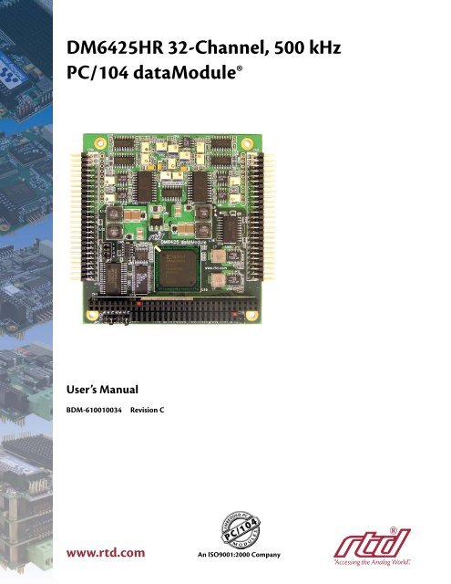
DM6425HR 32-Channel, 500 kHz<br />
PC/104 dataModule®<br />
User’s <strong>Manual</strong><br />
BDM-610010034<br />
Revision C<br />
www.rtd.com<br />
An ISO9001:2000 Company<br />
®<br />
“Accessing the Analog World” ®
DM6425HR 32-Channel, 500 kHz PC/104 dataModule® User’s <strong>Manual</strong><br />
<strong>RTD</strong> Document Number: BDM-610010034 Revision C<br />
Copyright © 2008 <strong>RTD</strong> <strong>Embedded</strong> <strong>Technologies</strong>, <strong>Inc</strong>. All rights reserved.<br />
Trademarks<br />
Advanced Digital I/O, aDIO, a2DIO, Autonomous SmartCal, cpuModule, dspFramework, dspModule, IDAN, HiDAN,<br />
HiDANplus, “MIL Value for COTS prices”, multiPort, and PC/104EZ are trademarks, and “Accessing the Analog World”,<br />
dataModule, <strong>RTD</strong>, and the <strong>RTD</strong> logo are registered trademarks of <strong>RTD</strong> <strong>Embedded</strong> <strong>Technologies</strong>, <strong>Inc</strong>. PS/2, PC/XT,<br />
PC/AT, and IBM are trademarks of International Business Machines <strong>Inc</strong>. MS-DOS, Windows, Windows 95, Windows 98,<br />
and Windows NT are trademarks of Microsoft Corp. Linux is a registered trademark of Linus Torvalds. M-Systems and<br />
DiskOnChip are trademarks or registered trademarks of M-Systems Flash Disk Pioneers, Ltd. PC/104 is a registered<br />
trademark of PC/104 Consortium. All other trademarks appearing in this document are the property of their respective<br />
owners.<br />
Contents and specifications within this manual are subject to change without notice.<br />
Revision Date Reason for Change<br />
A 2/23/06 Initial release.<br />
Revision History<br />
B 3/2/06 Corrected Write Register to show BA + 0x02h, bit 4, reserved; revised bit field description accordingly.<br />
C 11/5/08 Corrected examples in Special Considerations on page 111. Simplified formulas in Table 8, Analog<br />
Trigger Threshold Values—80<br />
ii DM6425HR dataModule BDM-610010034 Rev C
DM6425 32-Channel, 500 kHz<br />
PC/104 dataModule®<br />
www.rtd.com<br />
An ISO9001:2000 Company<br />
®<br />
“Accessing the Analog World” ®
Contact Information<br />
<strong>RTD</strong> <strong>Embedded</strong> <strong>Technologies</strong>, <strong>Inc</strong>.<br />
103 Innovation Blvd.<br />
State College, PA 16803-0906<br />
USA<br />
Phone: +1-814-234-8087<br />
Fax: +1-814-234-5218<br />
E-mail:<br />
sales@rtd.com<br />
techsupport@rtd.com<br />
Internet:<br />
http://www.rtd.com<br />
iv DM6425HR dataModule BDM-610010034 Rev C
Table of Contents<br />
Chapter 1 Introduction 1<br />
DM6425HR Ordering Information . . . . . . . . . . . . . . . . . . . . . . . . . . . . . . . . . . . . . . . . . . . . . . . . . . . . . . . . . . . . . . . . . . . . . . . . . . . 3<br />
DM6425HR Model Options . . . . . . . . . . . . . . . . . . . . . . . . . . . . . . . . . . . . . . . . . . . . . . . . . . . . . . . . . . . . . . . . . . . . . . . . . . . . . . . . . . 3<br />
DM6425HR Accessories . . . . . . . . . . . . . . . . . . . . . . . . . . . . . . . . . . . . . . . . . . . . . . . . . . . . . . . . . . . . . . . . . . . . . . . . . . . . . . . . . . . . . . 4<br />
Features . . . . . . . . . . . . . . . . . . . . . . . . . . . . . . . . . . . . . . . . . . . . . . . . . . . . . . . . . . . . . . . . . . . . . . . . . . . . . . . . . . . . . . . . . . . . . . . . . . . . . . . . 5<br />
Major Functions . . . . . . . . . . . . . . . . . . . . . . . . . . . . . . . . . . . . . . . . . . . . . . . . . . . . . . . . . . . . . . . . . . . . . . . . . . . . . . . . . . . . . . . . . . . . . . . 6<br />
Analog-to-Digital Conversion . . . . . . . . . . . . . . . . . . . . . . . . . . . . . . . . . . . . . . . . . . . . . . . . . . . . . . . . . . . . . . . . . . . . . . . . . . . . . . . . 7<br />
A/D Conversion Circuitry. . . . . . . . . . . . . . . . . . . . . . . . . . . . . . . . . . . . . . . . . . . . . . . . . . . . . . . . . . . . . . . . . . . . . . . . . . . . . . . . . . . . . 7<br />
Analog Inputs . . . . . . . . . . . . . . . . . . . . . . . . . . . . . . . . . . . . . . . . . . . . . . . . . . . . . . . . . . . . . . . . . . . . . . . . . . . . . . . . . . . . . . . . . . . . . . . 7<br />
Channel-Gain Scan Memory . . . . . . . . . . . . . . . . . . . . . . . . . . . . . . . . . . . . . . . . . . . . . . . . . . . . . . . . . . . . . . . . . . . . . . . . . . . . . . . . . 7<br />
A/D Converter. . . . . . . . . . . . . . . . . . . . . . . . . . . . . . . . . . . . . . . . . . . . . . . . . . . . . . . . . . . . . . . . . . . . . . . . . . . . . . . . . . . . . . . . . . . . . . . 8<br />
1024 Sample Buffer . . . . . . . . . . . . . . . . . . . . . . . . . . . . . . . . . . . . . . . . . . . . . . . . . . . . . . . . . . . . . . . . . . . . . . . . . . . . . . . . . . . . . . . . . . 8<br />
Data Transfer . . . . . . . . . . . . . . . . . . . . . . . . . . . . . . . . . . . . . . . . . . . . . . . . . . . . . . . . . . . . . . . . . . . . . . . . . . . . . . . . . . . . . . . . . . . . . . . . 8<br />
Digital-to-Analog Conversion . . . . . . . . . . . . . . . . . . . . . . . . . . . . . . . . . . . . . . . . . . . . . . . . . . . . . . . . . . . . . . . . . . . . . . . . . . . . . . . . 8<br />
8254 Timer/Counters . . . . . . . . . . . . . . . . . . . . . . . . . . . . . . . . . . . . . . . . . . . . . . . . . . . . . . . . . . . . . . . . . . . . . . . . . . . . . . . . . . . . . . . . . 9<br />
Digital I/O. . . . . . . . . . . . . . . . . . . . . . . . . . . . . . . . . . . . . . . . . . . . . . . . . . . . . . . . . . . . . . . . . . . . . . . . . . . . . . . . . . . . . . . . . . . . . . . . . . . . . . 10<br />
For More Information . . . . . . . . . . . . . . . . . . . . . . . . . . . . . . . . . . . . . . . . . . . . . . . . . . . . . . . . . . . . . . . . . . . . . . . . . . . . . . . . . . . . . . . . . 11<br />
Chapter 2 DM6425HR Module Settings 13<br />
Factory-Configured Jumper and Solder Blob Settings . . . . . . . . . . . . . . . . . . . . . . . . . . . . . . . . . . . . . . . . . . . . . . . . . . . . . 14<br />
JP1—CN3, Pin 43 Signal Select (Factory Setting: OT1) . . . . . . . . . . . . . . . . . . . . . . . . . . . . . . . . . . . . . . . . . . . . . . . . . . . . . . . . . 16<br />
JP2—User TC Clock Source Select<br />
(Factory Settings—CLK 0: XTAL; CLK 1: OT0). . . . . . . . . . . . . . . . . . . . . . . . . . . . . . . . . . . . . . . . . . . . . . . . . . . . . . . . . . . . . . . . . . . .16<br />
Base Address Jumper (Factory Setting: 300 hex, 768 decimal). . . . . . . . . . . . . . . . . . . . . . . . . . . . . . . . . . . . . . . . . . . . . . . . . . 17<br />
JS1, JS2, JS3, and JS4—Pull-Up/Pull-Down Resistors on Digital I/O Lines . . . . . . . . . . . . . . . . . . . . . . . . . . . . . . . . . . . . . . . . 18<br />
Chapter 3 Installing the dataModule 19<br />
DM6425HR Connectors. . . . . . . . . . . . . . . . . . . . . . . . . . . . . . . . . . . . . . . . . . . . . . . . . . . . . . . . . . . . . . . . . . . . . . . . . . . . . . . . . . . . . . . 20<br />
Installation Considerations. . . . . . . . . . . . . . . . . . . . . . . . . . . . . . . . . . . . . . . . . . . . . . . . . . . . . . . . . . . . . . . . . . . . . . . . . . . . . . . . . . . 21<br />
Before You Begin . . . . . . . . . . . . . . . . . . . . . . . . . . . . . . . . . . . . . . . . . . . . . . . . . . . . . . . . . . . . . . . . . . . . . . . . . . . . . . . . . . . . . . . . . . . . . . 21<br />
Installing the DM6425HR in a PC/104 Stack . . . . . . . . . . . . . . . . . . . . . . . . . . . . . . . . . . . . . . . . . . . . . . . . . . . . . . . . . . . . . . . . 22<br />
External I/O Connections. . . . . . . . . . . . . . . . . . . . . . . . . . . . . . . . . . . . . . . . . . . . . . . . . . . . . . . . . . . . . . . . . . . . . . . . . . . . . . . . . . . . . 23<br />
Connecting the Analog Input Pins. . . . . . . . . . . . . . . . . . . . . . . . . . . . . . . . . . . . . . . . . . . . . . . . . . . . . . . . . . . . . . . . . . . . . . . . . . . . 25<br />
Single-Ended Mode . . . . . . . . . . . . . . . . . . . . . . . . . . . . . . . . . . . . . . . . . . . . . . . . . . . . . . . . . . . . . . . . . . . . . . . . . . . . . . . . . . . . . 25<br />
Differential Mode . . . . . . . . . . . . . . . . . . . . . . . . . . . . . . . . . . . . . . . . . . . . . . . . . . . . . . . . . . . . . . . . . . . . . . . . . . . . . . . . . . . . . . . 26<br />
Connecting the Module for Simultaneous Sampling . . . . . . . . . . . . . . . . . . . . . . . . . . . . . . . . . . . . . . . . . . . . . . . . . . . . . . . . . . 28<br />
Connecting the Analog Outputs . . . . . . . . . . . . . . . . . . . . . . . . . . . . . . . . . . . . . . . . . . . . . . . . . . . . . . . . . . . . . . . . . . . . . . . . . . . . . 28<br />
Connecting the Timer/Counters and Digital I/O . . . . . . . . . . . . . . . . . . . . . . . . . . . . . . . . . . . . . . . . . . . . . . . . . . . . . . . . . . . . . . 28<br />
Chapter 4 I/O Mapping 29<br />
Defining the I/O Map . . . . . . . . . . . . . . . . . . . . . . . . . . . . . . . . . . . . . . . . . . . . . . . . . . . . . . . . . . . . . . . . . . . . . . . . . . . . . . . . . . . . . . . . . 30<br />
BDM-610010034 Rev C v
BA + 0x00h (0): Clear/Program Clear Register (Read/Write) . . . . . . . . . . . . . . . . . . . . . . . . . . . . . . . . . . . . . . . . . . . . . . . . . . . 36<br />
BA + 0x02h (2): Read Status/Program Control Register (Read/Write) . . . . . . . . . . . . . . . . . . . . . . . . . . . . . . . . . . . . . . . . . . 38<br />
BA + 0x04h (4): Read Converted Data/Load Channel-Gain and Digital Data (Read/Write). . . . . . . . . . . . . . . . . . . . . . 41<br />
Load Channel-Gain Latch (BA + 0x02h, bits 1 and 0 = 00) . . . . . . . . . . . . . . . . . . . . . . . . . . . . . . . . . . . . . . . . . . . . . . . . 41<br />
Load Channel-Gain Table in Channel-Gain Scan Memory<br />
(BA + 0x02h, bits 1 and 0 = 01) . . . . . . . . . . . . . . . . . . . . . . . . . . . . . . . . . . . . . . . . . . . . . . . . . . . . . . . . . . . . . . . . . . . . . . . . . . . . . . . . .43<br />
Load Digital Table in Channel-Gain Scan Memory (BA + 0x02h, bits 1 and 0 = 10). . . . . . . . . . . . . . . . . . . . . . . . . 44<br />
BA + 0x06h (6): Start Convert/Program Trigger Modes (Read/Write) . . . . . . . . . . . . . . . . . . . . . . . . . . . . . . . . . . . . . . . . . . 44<br />
BA + 0x08h (8): Program IRQ Source and Channel (Write) . . . . . . . . . . . . . . . . . . . . . . . . . . . . . . . . . . . . . . . . . . . . . . . . . . . . 46<br />
BA + 0x0Ah (10): Digital Input FIFO/Program Digital Input FIFO Configuration Register (Read/Write). . . . . . . . . . 47<br />
BA + 0x0Eh (14): A/D Sample Counter Trigger (Read) . . . . . . . . . . . . . . . . . . . . . . . . . . . . . . . . . . . . . . . . . . . . . . . . . . . . . . . . . 47<br />
BA + 0x10h (16): TC Counter 0 (Read/Write) . . . . . . . . . . . . . . . . . . . . . . . . . . . . . . . . . . . . . . . . . . . . . . . . . . . . . . . . . . . . . . . . . 48<br />
BA + 0x12h (18): TC Counter 1 (Read/Write) . . . . . . . . . . . . . . . . . . . . . . . . . . . . . . . . . . . . . . . . . . . . . . . . . . . . . . . . . . . . . . . . 48<br />
BA + 0x14h (20): TC Counter 2 (Read/Write) . . . . . . . . . . . . . . . . . . . . . . . . . . . . . . . . . . . . . . . . . . . . . . . . . . . . . . . . . . . . . . . . 48<br />
BA + 0x16h (22): Timer/Counter Control Word (Write Only). . . . . . . . . . . . . . . . . . . . . . . . . . . . . . . . . . . . . . . . . . . . . . . . . . 48<br />
BA + 0x18h (24): Digital I/O Port 0, Bit Programmable Port (Read/Write). . . . . . . . . . . . . . . . . . . . . . . . . . . . . . . . . . . . . . 49<br />
BA + 0x1Ah (26): Digital I/O Port 1, Byte Programmable Port (Read/Write). . . . . . . . . . . . . . . . . . . . . . . . . . . . . . . . . . . . 49<br />
BA + 0x1Ch (28): Read/Program Port 0 Direction/Mask/Compare Registers (Read/Write). . . . . . . . . . . . . . . . . . . . . . 49<br />
BA + 0x1Eh (30): Digital IRQ Status/Program Digital Mode<br />
(Ports 0 and 1, Read/Write) . . . . . . . . . . . . . . . . . . . . . . . . . . . . . . . . . . . . . . . . . . . . . . . . . . . . . . . . . . . . . . . . . . . . . . . . . . . . . . . . . . . . .51<br />
BA + 0x400h (1024): D/A Analog Setup (Read/Write) . . . . . . . . . . . . . . . . . . . . . . . . . . . . . . . . . . . . . . . . . . . . . . . . . . . . . . . . . 52<br />
BA + 0x402h (1026): Simutaneous Update Register (Write) . . . . . . . . . . . . . . . . . . . . . . . . . . . . . . . . . . . . . . . . . . . . . . . . . . . 52<br />
BA + 0x404h (1028): DAC1 Update Register (Write). . . . . . . . . . . . . . . . . . . . . . . . . . . . . . . . . . . . . . . . . . . . . . . . . . . . . . . . . . . 52<br />
BA + 0x406h (1030): DAC2 Update Register (Write). . . . . . . . . . . . . . . . . . . . . . . . . . . . . . . . . . . . . . . . . . . . . . . . . . . . . . . . . . . 52<br />
BA + 0x408h (1032): DAC3 Update Register (Write). . . . . . . . . . . . . . . . . . . . . . . . . . . . . . . . . . . . . . . . . . . . . . . . . . . . . . . . . . . 53<br />
BA + 0x40Ah (1034): DAC4 Update Register (Write) . . . . . . . . . . . . . . . . . . . . . . . . . . . . . . . . . . . . . . . . . . . . . . . . . . . . . . . . . . 53<br />
BA + 0x410h (1040): Analog Threshold Detector Setup (Read/Write). . . . . . . . . . . . . . . . . . . . . . . . . . . . . . . . . . . . . . . . . . 53<br />
BA + 0x418h (1048): Digital I/O Port 2, Bit Programmable Port (Read/Write) . . . . . . . . . . . . . . . . . . . . . . . . . . . . . . . . . . 54<br />
BA + 0x41Ah (1050): Digital I/O Port 3, Byte Programmable Port (Read/Write) . . . . . . . . . . . . . . . . . . . . . . . . . . . . . . . . 54<br />
BA + 0x41Ch (1052): Read/Program Port 2 Direction/Mask/Compare Registers (Read/Write) . . . . . . . . . . . . . . . . . . 55<br />
BA + 0x41Eh (1054): Digital IRQ Status/Program Digital Mode<br />
(Ports 2 and 3, Read/Write) . . . . . . . . . . . . . . . . . . . . . . . . . . . . . . . . . . . . . . . . . . . . . . . . . . . . . . . . . . . . . . . . . . . . . . . . . . . . . . . . . . . . .56<br />
BA + 0x800h/801h (2048/2049): Board ID Register (Read) . . . . . . . . . . . . . . . . . . . . . . . . . . . . . . . . . . . . . . . . . . . . . . . . . . . . . 57<br />
BA + 0x802h (2050): Board ID Reset (Read) . . . . . . . . . . . . . . . . . . . . . . . . . . . . . . . . . . . . . . . . . . . . . . . . . . . . . . . . . . . . . . . . . . . 57<br />
Programming the DM6425HR. . . . . . . . . . . . . . . . . . . . . . . . . . . . . . . . . . . . . . . . . . . . . . . . . . . . . . . . . . . . . . . . . . . . . . . . . . . . . . . . 58<br />
Clearing and Setting Bits in a Port . . . . . . . . . . . . . . . . . . . . . . . . . . . . . . . . . . . . . . . . . . . . . . . . . . . . . . . . . . . . . . . . . . . . . . . . . . . . 58<br />
Chapter 5 A/D Conversions 61<br />
Before Starting Conversions . . . . . . . . . . . . . . . . . . . . . . . . . . . . . . . . . . . . . . . . . . . . . . . . . . . . . . . . . . . . . . . . . . . . . . . . . . . . . . . . . . 62<br />
Initializing the Module . . . . . . . . . . . . . . . . . . . . . . . . . . . . . . . . . . . . . . . . . . . . . . . . . . . . . . . . . . . . . . . . . . . . . . . . . . . . . . . . . . . . . . . 62<br />
Programming Channel, Gain, Input Range, and Type . . . . . . . . . . . . . . . . . . . . . . . . . . . . . . . . . . . . . . . . . . . . . . . . . . . . . . . . . . 63<br />
Programming the Channel-Gain Table . . . . . . . . . . . . . . . . . . . . . . . . . . . . . . . . . . . . . . . . . . . . . . . . . . . . . . . . . . . . . . . . . . . . . . . . 64<br />
16-Bit A/D Table . . . . . . . . . . . . . . . . . . . . . . . . . . . . . . . . . . . . . . . . . . . . . . . . . . . . . . . . . . . . . . . . . . . . . . . . . . . . . . . . . . . . . . . . 64<br />
Channel Select, Gain Select, Input Range, and Input Type . . . . . . . . . . . . . . . . . . . . . . . . . . . . . . . . . . . . . . . . . . . . . . . . . . . . . 64<br />
Pause Bit . . . . . . . . . . . . . . . . . . . . . . . . . . . . . . . . . . . . . . . . . . . . . . . . . . . . . . . . . . . . . . . . . . . . . . . . . . . . . . . . . . . . . . . . . . . . . . . . . . . . 65<br />
Skip Bit . . . . . . . . . . . . . . . . . . . . . . . . . . . . . . . . . . . . . . . . . . . . . . . . . . . . . . . . . . . . . . . . . . . . . . . . . . . . . . . . . . . . . . . . . . . . . . . . . . . . . . 65<br />
8-Bit Digital Table . . . . . . . . . . . . . . . . . . . . . . . . . . . . . . . . . . . . . . . . . . . . . . . . . . . . . . . . . . . . . . . . . . . . . . . . . . . . . . . . . . . . . . . . . . . . 66<br />
Setting Up A/D and Digital Tables . . . . . . . . . . . . . . . . . . . . . . . . . . . . . . . . . . . . . . . . . . . . . . . . . . . . . . . . . . . . . . . . . . . . . . . . . . . . 66<br />
Using the Channel-Gain Table for A/D Conversions . . . . . . . . . . . . . . . . . . . . . . . . . . . . . . . . . . . . . . . . . . . . . . . . . . . . . . . . . . . 67<br />
Channel-Gain Table and Throughput Rates . . . . . . . . . . . . . . . . . . . . . . . . . . . . . . . . . . . . . . . . . . . . . . . . . . . . . . . . . . . . . . 67<br />
vi DM6425HR dataModule BDM-610010034 Rev C
A/D Conversion Modes . . . . . . . . . . . . . . . . . . . . . . . . . . . . . . . . . . . . . . . . . . . . . . . . . . . . . . . . . . . . . . . . . . . . . . . . . . . . . . . . . . . . . . . 68<br />
Start A/D Conversions . . . . . . . . . . . . . . . . . . . . . . . . . . . . . . . . . . . . . . . . . . . . . . . . . . . . . . . . . . . . . . . . . . . . . . . . . . . . . . . . . . . . . . . 68<br />
Start/Stop Trigger Select . . . . . . . . . . . . . . . . . . . . . . . . . . . . . . . . . . . . . . . . . . . . . . . . . . . . . . . . . . . . . . . . . . . . . . . . . . . . . . . . . . . . . 70<br />
Triggering a Burst Sample. . . . . . . . . . . . . . . . . . . . . . . . . . . . . . . . . . . . . . . . . . . . . . . . . . . . . . . . . . . . . . . . . . . . . . . . . . . . . . . . 70<br />
Trigger Repeat Function . . . . . . . . . . . . . . . . . . . . . . . . . . . . . . . . . . . . . . . . . . . . . . . . . . . . . . . . . . . . . . . . . . . . . . . . . . . . . . . . . 71<br />
Pacer Clock Source . . . . . . . . . . . . . . . . . . . . . . . . . . . . . . . . . . . . . . . . . . . . . . . . . . . . . . . . . . . . . . . . . . . . . . . . . . . . . . . . . . . . . . 71<br />
Types of Conversions. . . . . . . . . . . . . . . . . . . . . . . . . . . . . . . . . . . . . . . . . . . . . . . . . . . . . . . . . . . . . . . . . . . . . . . . . . . . . . . . . . . . . . . . . 71<br />
Single Conversion . . . . . . . . . . . . . . . . . . . . . . . . . . . . . . . . . . . . . . . . . . . . . . . . . . . . . . . . . . . . . . . . . . . . . . . . . . . . . . . . . . . . . . . 71<br />
Multiple Conversions. . . . . . . . . . . . . . . . . . . . . . . . . . . . . . . . . . . . . . . . . . . . . . . . . . . . . . . . . . . . . . . . . . . . . . . . . . . . . . . . . . . . 72<br />
Random Channel Scan . . . . . . . . . . . . . . . . . . . . . . . . . . . . . . . . . . . . . . . . . . . . . . . . . . . . . . . . . . . . . . . . . . . . . . . . . . . . . . . . . . 72<br />
Programmable Burst . . . . . . . . . . . . . . . . . . . . . . . . . . . . . . . . . . . . . . . . . . . . . . . . . . . . . . . . . . . . . . . . . . . . . . . . . . . . . . . . . . . . 73<br />
Programmable Multi-Scan. . . . . . . . . . . . . . . . . . . . . . . . . . . . . . . . . . . . . . . . . . . . . . . . . . . . . . . . . . . . . . . . . . . . . . . . . . . . . . . 73<br />
Starting an A/D Conversion . . . . . . . . . . . . . . . . . . . . . . . . . . . . . . . . . . . . . . . . . . . . . . . . . . . . . . . . . . . . . . . . . . . . . . . . . . . . . . . . . . 74<br />
Monitoring Conversion Status (FIFO Empty Flag or End-of-Convert) . . . . . . . . . . . . . . . . . . . . . . . . . . . . . . . . . . . . . . . . . . 74<br />
Halting Conversions. . . . . . . . . . . . . . . . . . . . . . . . . . . . . . . . . . . . . . . . . . . . . . . . . . . . . . . . . . . . . . . . . . . . . . . . . . . . . . . . . . . . . . . . . . 74<br />
Reading the Converted Data . . . . . . . . . . . . . . . . . . . . . . . . . . . . . . . . . . . . . . . . . . . . . . . . . . . . . . . . . . . . . . . . . . . . . . . . . . . . . . . . . 74<br />
Using the A/D Data Markers . . . . . . . . . . . . . . . . . . . . . . . . . . . . . . . . . . . . . . . . . . . . . . . . . . . . . . . . . . . . . . . . . . . . . . . . . . . . . . . . . 76<br />
Programming the Pacer Clock . . . . . . . . . . . . . . . . . . . . . . . . . . . . . . . . . . . . . . . . . . . . . . . . . . . . . . . . . . . . . . . . . . . . . . . . . . . . . . . . 76<br />
Selecting 16-bit or 32-bit Pacer Clock . . . . . . . . . . . . . . . . . . . . . . . . . . . . . . . . . . . . . . . . . . . . . . . . . . . . . . . . . . . . . . . . . . . . 76<br />
Programming Steps . . . . . . . . . . . . . . . . . . . . . . . . . . . . . . . . . . . . . . . . . . . . . . . . . . . . . . . . . . . . . . . . . . . . . . . . . . . . . . . . . . . . . 77<br />
Programming the Burst Clock . . . . . . . . . . . . . . . . . . . . . . . . . . . . . . . . . . . . . . . . . . . . . . . . . . . . . . . . . . . . . . . . . . . . . . . . . . . . . . . . 78<br />
Programming the Sample Counter . . . . . . . . . . . . . . . . . . . . . . . . . . . . . . . . . . . . . . . . . . . . . . . . . . . . . . . . . . . . . . . . . . . . . . . . . . . 78<br />
Using the Sample Counter to Create Large Data Arrays . . . . . . . . . . . . . . . . . . . . . . . . . . . . . . . . . . . . . . . . . . . . . . . . . . . 79<br />
Analog Trigger . . . . . . . . . . . . . . . . . . . . . . . . . . . . . . . . . . . . . . . . . . . . . . . . . . . . . . . . . . . . . . . . . . . . . . . . . . . . . . . . . . . . . . . . . . . . . . . . . 80<br />
Chapter 6 Data Transfers Using DMA 83<br />
Choosing a DMA Channel. . . . . . . . . . . . . . . . . . . . . . . . . . . . . . . . . . . . . . . . . . . . . . . . . . . . . . . . . . . . . . . . . . . . . . . . . . . . . . . . . . . . . 84<br />
Allocating a DMA Buffer . . . . . . . . . . . . . . . . . . . . . . . . . . . . . . . . . . . . . . . . . . . . . . . . . . . . . . . . . . . . . . . . . . . . . . . . . . . . . . . . . . . . . . 85<br />
Calculating the Page and Offset of a Buffer . . . . . . . . . . . . . . . . . . . . . . . . . . . . . . . . . . . . . . . . . . . . . . . . . . . . . . . . . . . . . . . . . 85<br />
Setting the DMA Page Register . . . . . . . . . . . . . . . . . . . . . . . . . . . . . . . . . . . . . . . . . . . . . . . . . . . . . . . . . . . . . . . . . . . . . . . . . . . . . . . 87<br />
The DMA Controller . . . . . . . . . . . . . . . . . . . . . . . . . . . . . . . . . . . . . . . . . . . . . . . . . . . . . . . . . . . . . . . . . . . . . . . . . . . . . . . . . . . . . . . . . . 87<br />
DMA Mask Register . . . . . . . . . . . . . . . . . . . . . . . . . . . . . . . . . . . . . . . . . . . . . . . . . . . . . . . . . . . . . . . . . . . . . . . . . . . . . . . . . . . . . . . . . . . 88<br />
DMA Mode Register . . . . . . . . . . . . . . . . . . . . . . . . . . . . . . . . . . . . . . . . . . . . . . . . . . . . . . . . . . . . . . . . . . . . . . . . . . . . . . . . . . . . . . . . . . . 88<br />
Programming the DMA Controller . . . . . . . . . . . . . . . . . . . . . . . . . . . . . . . . . . . . . . . . . . . . . . . . . . . . . . . . . . . . . . . . . . . . . . . . . . 88<br />
Programming the DM6425HR for DMA . . . . . . . . . . . . . . . . . . . . . . . . . . . . . . . . . . . . . . . . . . . . . . . . . . . . . . . . . . . . . . . . . . . . . 89<br />
Monitoring for DMA Done . . . . . . . . . . . . . . . . . . . . . . . . . . . . . . . . . . . . . . . . . . . . . . . . . . . . . . . . . . . . . . . . . . . . . . . . . . . . . . . . . . . 89<br />
Dual DMA Mode. . . . . . . . . . . . . . . . . . . . . . . . . . . . . . . . . . . . . . . . . . . . . . . . . . . . . . . . . . . . . . . . . . . . . . . . . . . . . . . . . . . . . . . . . . . . . . . 89<br />
Common DMA Problems . . . . . . . . . . . . . . . . . . . . . . . . . . . . . . . . . . . . . . . . . . . . . . . . . . . . . . . . . . . . . . . . . . . . . . . . . . . . . . . . . . . . . 89<br />
Chapter 7 Interrupts 91<br />
Software Selectable Interrupt Sources . . . . . . . . . . . . . . . . . . . . . . . . . . . . . . . . . . . . . . . . . . . . . . . . . . . . . . . . . . . . . . . . . . . . . . 92<br />
Software Selectable Interrupt Channel. . . . . . . . . . . . . . . . . . . . . . . . . . . . . . . . . . . . . . . . . . . . . . . . . . . . . . . . . . . . . . . . . . . . . . 92<br />
Advanced Digital Interrupts. . . . . . . . . . . . . . . . . . . . . . . . . . . . . . . . . . . . . . . . . . . . . . . . . . . . . . . . . . . . . . . . . . . . . . . . . . . . . . . . . . 92<br />
Event Mode . . . . . . . . . . . . . . . . . . . . . . . . . . . . . . . . . . . . . . . . . . . . . . . . . . . . . . . . . . . . . . . . . . . . . . . . . . . . . . . . . . . . . . . . . . . . . . . . . 92<br />
Match Mode . . . . . . . . . . . . . . . . . . . . . . . . . . . . . . . . . . . . . . . . . . . . . . . . . . . . . . . . . . . . . . . . . . . . . . . . . . . . . . . . . . . . . . . . . . . . . . . . 92<br />
BDM-610010034 Rev C vii
Sampling Digital Lines for Change of State . . . . . . . . . . . . . . . . . . . . . . . . . . . . . . . . . . . . . . . . . . . . . . . . . . . . . . . . . . . . . . . . . . . . 92<br />
Basic Programming For Interrupt Handling . . . . . . . . . . . . . . . . . . . . . . . . . . . . . . . . . . . . . . . . . . . . . . . . . . . . . . . . . . . . . . . . 93<br />
What Is an Interrupt? . . . . . . . . . . . . . . . . . . . . . . . . . . . . . . . . . . . . . . . . . . . . . . . . . . . . . . . . . . . . . . . . . . . . . . . . . . . . . . . . . . . . . . . . 93<br />
Interrupt Request Lines . . . . . . . . . . . . . . . . . . . . . . . . . . . . . . . . . . . . . . . . . . . . . . . . . . . . . . . . . . . . . . . . . . . . . . . . . . . . . . . . . . . . . . 93<br />
8259 Programmable Interrupt Controllers . . . . . . . . . . . . . . . . . . . . . . . . . . . . . . . . . . . . . . . . . . . . . . . . . . . . . . . . . . . . . . . . . . . . 93<br />
Interrupt Mask Registers (IMR) . . . . . . . . . . . . . . . . . . . . . . . . . . . . . . . . . . . . . . . . . . . . . . . . . . . . . . . . . . . . . . . . . . . . . . . . . . . . . . . 94<br />
End-of-Interrupt (EOI) Command . . . . . . . . . . . . . . . . . . . . . . . . . . . . . . . . . . . . . . . . . . . . . . . . . . . . . . . . . . . . . . . . . . . . . . . . . . . . 94<br />
What Happens When an Interrupt Occurs? . . . . . . . . . . . . . . . . . . . . . . . . . . . . . . . . . . . . . . . . . . . . . . . . . . . . . . . . . . . . . . . . . . . 94<br />
Using Interrupts in Your Programs. . . . . . . . . . . . . . . . . . . . . . . . . . . . . . . . . . . . . . . . . . . . . . . . . . . . . . . . . . . . . . . . . . . . . . . . . . . . 94<br />
Writing an Interrupt Service Routine (ISR) . . . . . . . . . . . . . . . . . . . . . . . . . . . . . . . . . . . . . . . . . . . . . . . . . . . . . . . . . . . . . . . . . . . . 94<br />
Saving the Startup Interrupt Mask Register (IMR) and Interrupt Vector. . . . . . . . . . . . . . . . . . . . . . . . . . . . . . . . . . . . . . . . 96<br />
Restoring the Startup IMR and Interrupt Vector . . . . . . . . . . . . . . . . . . . . . . . . . . . . . . . . . . . . . . . . . . . . . . . . . . . . . . . . . . . . . . 97<br />
Common Interrupt Mistakes . . . . . . . . . . . . . . . . . . . . . . . . . . . . . . . . . . . . . . . . . . . . . . . . . . . . . . . . . . . . . . . . . . . . . . . . . . . . . . . . . 97<br />
Chapter 8 D/A Conversions 99<br />
Chapter 9 Timer/Counters 101<br />
Chapter 10 Digital I/O 105<br />
Port 0, Bit Programmable Digital I/O. . . . . . . . . . . . . . . . . . . . . . . . . . . . . . . . . . . . . . . . . . . . . . . . . . . . . . . . . . . . . . . . . . . . . . . . 106<br />
Direction Register: . . . . . . . . . . . . . . . . . . . . . . . . . . . . . . . . . . . . . . . . . . . . . . . . . . . . . . . . . . . . . . . . . . . . . . . . . . . . . . . . . . . . . . . . . . . 106<br />
Advanced Digital Interrupts: Mask and Compare Registers . . . . . . . . . . . . . . . . . . . . . . . . . . . . . . . . . . . . . . . . . . . . . . . . . . . . 106<br />
Port 1, Port Programmable Digital I/O . . . . . . . . . . . . . . . . . . . . . . . . . . . . . . . . . . . . . . . . . . . . . . . . . . . . . . . . . . . . . . . . . . . . . . 106<br />
Port 2, Bit Programmable Digital I/O. . . . . . . . . . . . . . . . . . . . . . . . . . . . . . . . . . . . . . . . . . . . . . . . . . . . . . . . . . . . . . . . . . . . . . . . 106<br />
Direction Register: . . . . . . . . . . . . . . . . . . . . . . . . . . . . . . . . . . . . . . . . . . . . . . . . . . . . . . . . . . . . . . . . . . . . . . . . . . . . . . . . . . . . . . . . . . . 106<br />
Advanced Digital Interrupts: Mask and Compare Registers . . . . . . . . . . . . . . . . . . . . . . . . . . . . . . . . . . . . . . . . . . . . . . . . . . . . 106<br />
Port 3, Port Programmable Digital I/O . . . . . . . . . . . . . . . . . . . . . . . . . . . . . . . . . . . . . . . . . . . . . . . . . . . . . . . . . . . . . . . . . . . . . . 107<br />
Resetting the Digital Circuitry . . . . . . . . . . . . . . . . . . . . . . . . . . . . . . . . . . . . . . . . . . . . . . . . . . . . . . . . . . . . . . . . . . . . . . . . . . . . . . . 107<br />
Strobing Data into Port 0 . . . . . . . . . . . . . . . . . . . . . . . . . . . . . . . . . . . . . . . . . . . . . . . . . . . . . . . . . . . . . . . . . . . . . . . . . . . . . . . . . . . . . 107<br />
High-Speed Digital Input . . . . . . . . . . . . . . . . . . . . . . . . . . . . . . . . . . . . . . . . . . . . . . . . . . . . . . . . . . . . . . . . . . . . . . . . . . . . . . . . . . . . . 107<br />
Appendix A Example Programs 109<br />
Controlling the DM6425HR via Software. . . . . . . . . . . . . . . . . . . . . . . . . . . . . . . . . . . . . . . . . . . . . . . . . . . . . . . . . . . . . . . . . . . . 110<br />
<strong>RTD</strong> Provided Software . . . . . . . . . . . . . . . . . . . . . . . . . . . . . . . . . . . . . . . . . . . . . . . . . . . . . . . . . . . . . . . . . . . . . . . . . . . . . . . . . . . . . . 110<br />
Direct Register Control. . . . . . . . . . . . . . . . . . . . . . . . . . . . . . . . . . . . . . . . . . . . . . . . . . . . . . . . . . . . . . . . . . . . . . . . . . . . . . . . . . . . . . . 110<br />
Special Considerations . . . . . . . . . . . . . . . . . . . . . . . . . . . . . . . . . . . . . . . . . . . . . . . . . . . . . . . . . . . . . . . . . . . . . . . . . . . . . . . . . . . . . . . 111<br />
Appendix B Calibration 113<br />
Required Equipment . . . . . . . . . . . . . . . . . . . . . . . . . . . . . . . . . . . . . . . . . . . . . . . . . . . . . . . . . . . . . . . . . . . . . . . . . . . . . . . . . . . . . . . . . . 114<br />
A/D Calibration. . . . . . . . . . . . . . . . . . . . . . . . . . . . . . . . . . . . . . . . . . . . . . . . . . . . . . . . . . . . . . . . . . . . . . . . . . . . . . . . . . . . . . . . . . . . . . . . 115<br />
Bipolar Calibration. . . . . . . . . . . . . . . . . . . . . . . . . . . . . . . . . . . . . . . . . . . . . . . . . . . . . . . . . . . . . . . . . . . . . . . . . . . . . . . . . . . . . . . . . . . 115<br />
Bipolar Range Adjustment: –5 to +5 V . . . . . . . . . . . . . . . . . . . . . . . . . . . . . . . . . . . . . . . . . . . . . . . . . . . . . . . . . . . . . . . . . . . 115<br />
Bipolar Range Adjustment: –10 to +10 V . . . . . . . . . . . . . . . . . . . . . . . . . . . . . . . . . . . . . . . . . . . . . . . . . . . . . . . . . . . . . . . . 115<br />
Unipolar Calibration . . . . . . . . . . . . . . . . . . . . . . . . . . . . . . . . . . . . . . . . . . . . . . . . . . . . . . . . . . . . . . . . . . . . . . . . . . . . . . . . . . . . . . . . . 116<br />
Gain Adjustment . . . . . . . . . . . . . . . . . . . . . . . . . . . . . . . . . . . . . . . . . . . . . . . . . . . . . . . . . . . . . . . . . . . . . . . . . . . . . . . . . . . . . . . . . . . . 117<br />
viii DM6425HR dataModule BDM-610010034 Rev C
D/A Calibration. . . . . . . . . . . . . . . . . . . . . . . . . . . . . . . . . . . . . . . . . . . . . . . . . . . . . . . . . . . . . . . . . . . . . . . . . . . . . . . . . . . . . . . . . . . . . . . . 118<br />
Appendix C Specifications 119<br />
Appendix D I/O Connector Pin Assignments 123<br />
Appendix E IDAN Dimensions and Pinout 127<br />
IDAN-DM6425HR-62S . . . . . . . . . . . . . . . . . . . . . . . . . . . . . . . . . . . . . . . . . . . . . . . . . . . . . . . . . . . . . . . . . . . . . . . . . . . . . . . . . . . . . . . . 128<br />
IDAN-DM6425HR-62S Dimensions and Connector . . . . . . . . . . . . . . . . . . . . . . . . . . . . . . . . . . . . . . . . . . . . . . . . . . . . . . . . . . . 128<br />
IDAN-DM6425HR-62S External I/O Connections . . . . . . . . . . . . . . . . . . . . . . . . . . . . . . . . . . . . . . . . . . . . . . . . . . . . . . . . . . . . . 129<br />
IDAN-DM6425HR-68S . . . . . . . . . . . . . . . . . . . . . . . . . . . . . . . . . . . . . . . . . . . . . . . . . . . . . . . . . . . . . . . . . . . . . . . . . . . . . . . . . . . . . . . . 130<br />
IDAN-DM6425HR-68S Dimensions and Connector . . . . . . . . . . . . . . . . . . . . . . . . . . . . . . . . . . . . . . . . . . . . . . . . . . . . . . . . . . . 130<br />
IDAN-DM6425HR-68S External I/O Connections . . . . . . . . . . . . . . . . . . . . . . . . . . . . . . . . . . . . . . . . . . . . . . . . . . . . . . . . . . . . . 131<br />
Appendix F Limited Warranty 133<br />
BDM-610010034 Rev C ix
x DM6425HR dataModule BDM-610010034 Rev C
Chapter 1<br />
Introduction<br />
The DM6425HR 32-channel, 12-bit, 500 kHz PC/104 dataModule turns your IBM AT-compatible cpuModule or<br />
other PC/104 computer into a high-speed, high performance data acquisition and control system.<br />
This manual is intended to help you install your new module and get it running quickly, while also providing<br />
enough detail about the module and its functions so that you can enjoy maximum use of its features even in the<br />
most complex applications. <strong>RTD</strong> assumes that you already have an understanding of data acquisition principles<br />
and that you can customize the example software or write your own application programs.<br />
This manual is organized as follows:<br />
Chapter 1<br />
Chapter 2<br />
Chapter 3<br />
Chapter 4<br />
Chapter 5<br />
Chapter 6<br />
Chapter 7<br />
Chapter 8<br />
Chapter 9<br />
Chapter 10<br />
Appendix A<br />
Appendix B<br />
Appendix C<br />
Appendix D<br />
Appendix E<br />
Appendix F<br />
Introduction<br />
introduces main features and specifications<br />
DM6425HR Module Settings<br />
provides information on factory-default and user-configurable jumper settings<br />
Installing the dataModule<br />
provides information on installing the DM6425HR<br />
I/O Mapping<br />
describes the I/O map for the DM6425HR<br />
A/D Conversions<br />
shows how to program the DM6425HR to perform A/D conversions and read the results<br />
Data Transfers Using DMA<br />
explains how data transfers are accomplished using Direct Memory Access (DMA)<br />
Interrupts<br />
explains software selectable interrupts, digital interrupts, and basic interrupt programming<br />
D/A Conversions<br />
explains how to perform D/A conversions on the DM6425HR<br />
Timer/Counters<br />
explains the two 8254 timer/counter circuits on the DM6425HR<br />
Digital I/O<br />
explains the bit- and port-programmable digital I/O circuitry on the DM6425HR<br />
Example Programs<br />
discusses the example programs included with the DM6425HR<br />
Calibration<br />
describes how to calibrate the DM6425HR using the 6425DIAG diagnostic program<br />
included in the example software package, and using the trimpots on the dataModule<br />
Specifications<br />
provides the typical characteristics of the DM6425HR<br />
I/O Connector Pin Assignments<br />
provides the pinout for the DM6425HR I/O connectors<br />
IDAN Dimensions and Pinout<br />
provides connector pinouts for the DM6425HR installed in an <strong>RTD</strong> Intelligent Data<br />
Acquisition Node (IDAN) frame<br />
Limited Warranty<br />
BDM-610010034 Rev C Chapter 1: Introduction 1
50-pin<br />
I/O Header<br />
50-pin<br />
I/O Header<br />
PC/104 Bus (XT)<br />
PC/104 Bus (AT)<br />
Figure 1<br />
DM6425HR dataModule (top view)<br />
2 DM6425HR dataModule BDM-610010034 Rev C
DM6425HR Ordering Information<br />
The DM6425HR 32-channel, 12-bit, 500 kHz PC/104 dataModule is available with both a 1K FIFO buffer and an<br />
8K FIFO buffer. The DM6425HR can also be purchased as part of an Intelligent Data Acquisition Node (IDAN)<br />
building block, which consists of the dataModule and a milled aluminum IDAN frame. The IDAN building block<br />
can be used in just about any combination with other IDAN building blocks to create a simple but rugged<br />
PC/104 stack. Refer to Appendix E, IDAN Dimensions and Pinout, for more information. The DM6425HR can also<br />
be purchased as part of a custom-built <strong>RTD</strong> HiDAN or HiDANplus High Reliability Intelligent Data Acquisition<br />
Node. Contact <strong>RTD</strong> for more information on its high reliability PC/PCI-104 systems.<br />
DM6425HR Model Options<br />
The DM6425HR model options are shown below. Refer to the <strong>RTD</strong> website (www.rtd.com) for more detailed<br />
ordering information.<br />
Table 1<br />
DM6425HR dataModule Options<br />
Part Number<br />
DM6425HR-1<br />
DM6425HR-8<br />
Description<br />
32-channel, 12-bit, 500 kHz PC/104 dataModule with a 1K FIFO buffer on A/D converter<br />
32-channel, 12-bit, 500 kHz PC/104 dataModule with an 8K FIFO buffer on A/D converter<br />
Each DM6425HR package contains the following items:<br />
• DM6425HR dataModule<br />
• Companion CD containing software and documentation<br />
BDM-610010034 Rev C Chapter 1: Introduction 3
DM6425HR Accessories<br />
In addition to the items included in your DM6425HR package, several software and hardware accessories are<br />
available. <strong>Hardware</strong> accessories include IDAN frames, power supplies, terminal boards, and other connection<br />
systems. Contact <strong>RTD</strong> or your distributor, or visit the <strong>RTD</strong> website at www.rtd.com, for more information and for<br />
advice on selecting the most appropriate application software, drivers, and hardware accessories to support your<br />
control system.<br />
Table 2 Recommended Accessories 1<br />
Part Number<br />
XT50<br />
TB50<br />
XB50<br />
TMX32<br />
OP8/OP16<br />
MR8/MR16<br />
OR16<br />
TS16<br />
DM16<br />
Description<br />
3-foot, 50-pin, twisted-pair cable<br />
50-pin screw terminal board<br />
50-pin screw terminal extender board<br />
Analog input expansion board with thermocouple compensation (can expand a single input channel<br />
to 16 differential or 32 single-ended input channels)<br />
Opto-isolated, digital input boards (provide 8/16 opto-isolated digital inputs)<br />
Mechanical relay output boards (provide 8/16 electro-mechanical relay outputs)<br />
Mechanical relay and opto-isolated input board (provides 8 electro-mechanical relays outputs and<br />
8 opto-isolated digital inputs)<br />
J or K thermocouple input expansion board (multiplexes 16 differential thermocouple inputs into<br />
one channel)<br />
PC/104 to ISA bus extender board for testing your module in a conventional desktop computer<br />
1. Refer to the <strong>RTD</strong> website (www.rtd.com) for more details.<br />
4 DM6425HR dataModule BDM-610010034 Rev C
Features<br />
The DM6425HR is a 12-bit, 500 kHz analog I/O dataModule with either 16 differential or 32 single-ended analog<br />
input channels, 4 analog output channels, and 4 independent 8-bit digital I/O ports.<br />
Ultra-compact for embedded and portable applications, the DM6425HR complete feature set includes:<br />
• Analog threshold triggering on any one channel<br />
• 16 differential or 32 single-ended analog input channels<br />
• 12-bit, 2 μs analog-to-digital converter with 500 kHz throughput<br />
• Programmable input ranges: ± 5, ± 10, or 0 to +10 V<br />
• Programmable gains of 1, 2, 4, and 8<br />
• 1024 x 24 channel-gain scan memory with skip bit<br />
• Software, pacer clock, and external trigger modes<br />
• Scan, burst, and multi-burst using the channel-gain table<br />
• 16-bit programmable high-speed sample counter<br />
• A/D DMA transfer<br />
• 1024 sample A/D buffer for gap-free, high-speed sampling under Windows and DOS<br />
• Pre-, post-, and about-trigger modes<br />
• 3-bit analog input data/trigger marker<br />
• two 8-bit programmable digital I/O lines with Advanced Digital Interrupt modes<br />
• 1024 sample digital input buffer for gap-free, high-speed sampling under Windows and DOS<br />
• two byte programmable digital I/O lines<br />
• Six 16-bit timer/counters (two available to user) and onboard 8 MHz clock<br />
• Four 12-bit D/A output channels<br />
• ± 5, 0 to +5, ±10, or 0 to +10 V analog output range<br />
• Programmable interrupt source<br />
• +5 V operation<br />
• Windows and Linux® example programs<br />
• DOS example programs with source code<br />
• Diagnostics software<br />
BDM-610010034 Rev C Chapter 1: Introduction 5
Major Functions<br />
The DM6425HR has four major circuits:<br />
• the A/D<br />
• the D/A<br />
• the timer/counters<br />
• the digital I/O lines<br />
The following sections describe these circuits. Subsequent chapters provide a detailed discussion of module<br />
functions. Figure 2 provides a block diagram of the DM6425HR.<br />
DATA<br />
DMA<br />
CONTROL<br />
AND<br />
SELECT<br />
FIFO<br />
1024 X 16<br />
12-BIT<br />
A/D<br />
CONVERTER<br />
RANGE<br />
SELECT<br />
±5V<br />
0TO+5V<br />
0 TO +10 V<br />
CHANNEL/GAIN<br />
SCAN MEMORY<br />
AND CONTROL<br />
PROGRAM-<br />
MABLE<br />
GAIN<br />
AMPLIFIER<br />
1/2/4/8<br />
MUX<br />
16<br />
16<br />
3<br />
16 ANALOG INPUTS<br />
8 DIFF/16 SE<br />
–5 TO +5V<br />
0 TO +10V<br />
–10V TO +10V 16 ANALOG INPUTS<br />
8 DIFF/16 SE<br />
–5 TO +5V<br />
0 TO +10V<br />
–10V TO +10V<br />
DATA MARKERS<br />
PC/104 Bus<br />
ADDRESS<br />
INTERRUPT<br />
SELECT<br />
ADDRESS<br />
DECODE<br />
CONTROL<br />
PACER/<br />
BURST<br />
CLOCK<br />
8254<br />
PIT<br />
DIGITAL<br />
I/O<br />
TRIGGER<br />
CONTROL<br />
6<br />
PULL UP/DOWN<br />
RESISTORS<br />
P1.0 – P1.7 8<br />
HIGH SPEED SAMPLE<br />
COUNTER<br />
TIMER<br />
I/O<br />
SELECT<br />
P2.0 – P2.7 8<br />
8 MHz<br />
OSC<br />
8<br />
P3.0 – P3.7<br />
8<br />
TRIGGER IN<br />
EXT PACER CLK<br />
5 TIMER I/O<br />
8<br />
MUX<br />
I/O CONNECTOR (CN3)<br />
I/O CONNECTOR (CN4)<br />
P0.0 – P0.7<br />
8<br />
FIFO<br />
1024 X 8<br />
EVENT/MATCH<br />
INTERRUPT<br />
EVENT/MATCH<br />
INTERRUPT<br />
12-BIT<br />
D/A<br />
CONVERTER<br />
RANGE<br />
SELECT<br />
±5V/ ±10V<br />
0TO+5V<br />
0 TO +10 V<br />
AOUT 1<br />
AOUT 2<br />
12-BIT<br />
D/A<br />
CONVERTER<br />
RANGE<br />
SELECT<br />
±5V/ ±10V<br />
0TO+5V<br />
0 TO +10 V<br />
+5 VOLTS<br />
±12 VOLTS<br />
DC/DC<br />
CONVERTER ±15 VOLTS<br />
±12 VOLTS<br />
AOUT 3<br />
AOUT 4<br />
CONTROL<br />
+5 VOLTS<br />
+5 VOLTS<br />
±12 VOLTS<br />
DC/DC<br />
CONVERTER ±15 VOLTS<br />
±12 VOLTS<br />
CONTROL<br />
+5 VOLTS<br />
Figure 2<br />
DM6425HR Block Diagram<br />
6 DM6425HR dataModule BDM-610010034 Rev C
Analog-to-Digital Conversion<br />
The DM6425HR is software configurable on a channel-by-channel basis for up to 16 differential or 32 singleended<br />
analog inputs. Software programmable unipolar and bipolar input ranges and gains allow easy interfacing<br />
to a wide range of sensors. Overvoltage protection to ± 12 V is provided at the inputs. The common mode input<br />
voltage for differential operation is ± 10 V.<br />
Analog-to-digital (A/D) conversions are typically performed in 2 μs, and the maximum throughput rate of the<br />
board is 500 kHz. Conversions are controlled by software command, by an onboard pacer clock, by using triggers<br />
to start and stop sampling, or by using the sample counter to acquire a specified number of samples. Several<br />
trigger sources can be used to turn the pacer clock on and off, giving you exceptional flexibility in data<br />
acquisition. Scan, burst, and multi-burst modes are supported by using the channel-gain scan memory. A first in,<br />
first out (FIFO) sample buffer helps your computer manage the high throughput rate of the A/D converter by<br />
acting as an elastic storage bin for the converted data. Even if the computer does not read the data as fast as<br />
conversions are performed, conversions can continue until the FIFO is full.<br />
The converted data can be transferred to PC memory in one of three ways. Direct Memory Access (DMA)<br />
transfer supports conversion rates of up to 500,000 samples per second. Data also can be transferred using the<br />
programmed I/O mode or the interrupt mode. A special interrupt mode using a REP INS (Repeat Input String)<br />
instruction supports very high-speed data transfers. By generating an interrupt when the FIFO’s half-full flag is<br />
set, a REP INS instruction can be executed, transferring data to PC memory and emptying the FIFO buffer at the<br />
maximum rate allowed by the data bus.<br />
The mode of transfer and DMA channel are chosen through software. The PC data bus is used to read and/or<br />
transfer data to PC memory. In the DMA transfer mode, you can make continuous transfers directly to PC<br />
memory without going through the processor.<br />
A/D Conversion Circuitry<br />
The DM6425HR performs analog-to-digital conversions on up to 16 software-selectable analog input channels.<br />
Analog Inputs<br />
The input voltage range is software programmable for –5 to +5 V, –10 to +10 V, or 0 to +10 V. Softwareprogrammable<br />
binary gains of 1, 2, 4, and 8 let you amplify lower level signals to more closely match the module’s<br />
input ranges. Overvoltage protection to ±12 V is provided at the inputs.<br />
Channel-Gain Scan Memory<br />
The channel-gain scan memory lets you sample channels in any order, at high speeds, with a different gain on<br />
each channel. This 1024 x 24-bit memory supports complex channel-gain scan sequences, including digital<br />
output control. Using the digital output control feature, you can control external input expansion boards such<br />
as the TMX32 to expand channel capacity up to 512 channels. When used, these control lines are output on<br />
Port 1. When the digital lines are not used for this feature, they are available for other digital control functions.<br />
A skip bit is provided in the channel-gain data word to support different sampling rates on different channels.<br />
When this bit is set, the A/D conversion is not written to the FIFO on the selected channel. Chapter 4 and<br />
Chapter 5 describe this feature in detail.<br />
BDM-610010034 Rev C Chapter 1: Introduction 7
A/D Converter<br />
The 12-bit successive approximation A/D converter accurately digitizes dynamic input voltages in 2 μs, for a<br />
maximum throughput rate of 500 kHz. The converter IC contains a sample-and-hold amplifier, a 12-bit A/D<br />
converter, a 2.5 V reference, a clock, and a digital interface to provide complete A/D conversion on a single chip.<br />
Its low power CMOS logic combined with a high-precision, low-noise design provides accurate results.<br />
Conversions are controlled by software command, by pacer clock, by using triggers to start and stop sampling,<br />
or by the sample counter to acquire a specified number of samples. An onboard or external pacer clock can be<br />
used to control the conversion rate. Chapter 5, A/D Conversions, describes conversion modes.<br />
1024 Sample Buffer<br />
A first in, first out (FIFO) 1024 sample buffer helps your computer manage the high throughput rate of the A/D<br />
converter by providing an elastic storage bin for the converted data. Even if the computer does not read the data<br />
as fast as conversions are performed, conversions will continue until a FIFO full flag is sent to stop the converter.<br />
The sample buffer does not need to be addressed when you are writing to or reading from it; internal addressing<br />
makes sure that the data is properly stored and retrieved. All data accumulated in the sample buffer is stored<br />
intact until the PC is able to complete the data transfer. Its asynchronous operation means that data can be<br />
written to or read from it at any time, at any rate. When a transfer does begin, the data first placed in the FIFO is<br />
the first data out.<br />
Data Transfer<br />
The converted data can be transferred to PC memory in one of three ways. Direct Memory Access (DMA)<br />
transfer supports conversion rates of up to 500,000 samples per second. Data also can be transferred using the<br />
programmed I/O mode or the interrupt mode. A special interrupt mode using a REP INS (Repeat Input String)<br />
instruction supports very high-speed data transfers. By generating an interrupt when the FIFO’s half full flag is<br />
set or when the sample counter counts down, a REP INS instruction can be executed, transferring data to PC<br />
memory and emptying the sample buffer at the maximum rate allowed by the data bus.<br />
The PC data bus is used to read and/or transfer data to PC memory. In the DMA transfer mode, you can make<br />
continuous transfers directly to PC memory without going through the processor.<br />
The converted data plus a sign bit is stored in the top 13 bits (left-justified) of the 16-bit data word written to<br />
the sample buffer. The bottom three bits can be used as a 3-bit data marker as described in Chapter 5.<br />
Digital-to-Analog Conversion<br />
The digital-to-analog (D/A) circuitry features four independent 12-bit analog output channels with softwareselectable<br />
output ranges of ± 5, 0 to +5, ±10, or 0 to +10 V. The 5 V range has a resolution of 1.22 mV, the 10 V<br />
ranges have a resolution of 2.44 mV, and the 20 V range has a resolution of 4.88 mV.<br />
Data is programmed into the D/A converter by writing one 12-bit value. D/A outputs are automatically updated<br />
when the data is written. Access through DMA is not available. By setting a bit in a register, all of the D/As can<br />
be simultaneously updated, if so desired.<br />
8 DM6425HR dataModule BDM-610010034 Rev C
8254 Timer/Counters<br />
Two 8254 programmable interval timers provide six (three each) 16-bit, 8 MHz timer/counters to support a wide<br />
range of board operations and user timing and counting functions.<br />
One 8254 is the Clock TC, which is used for board operations. Two of its 16-bit timer/counters, Counter 0 and<br />
Counter 1, are cascaded and used internally for the pacer clock. The pacer clock is described in Chapter 5. The<br />
third timer/counter in the Clock TC, Counter 2, is the burst clock. Figure 3 shows the Clock TC circuitry.<br />
The other 8254 is the User TC, which has two 16-bit timer/counters (Counter 0 and Counter 1) for user functions<br />
and one 16-bit timer/counter (Counter 2) for the sample counter. Figure 4 shows the User TC circuitry.<br />
Each 16-bit timer/counter has two inputs, CLK in and GATE in, and one output, timer/counter OUT. Each can<br />
be programmed as binary or BCD down counters by writing the appropriate data to the command word, as<br />
described in Chapter 4. The command word also lets you set up the mode of operation. The six programmable<br />
modes are:<br />
Mode 0<br />
Mode 1<br />
Mode 2<br />
Mode 3<br />
Mode 4<br />
Mode 5<br />
Event Counter (Interrupt on Terminal Count)<br />
<strong>Hardware</strong>-Retriggerable One-Shot<br />
Rate Generator<br />
Square Wave Mode<br />
Software-Triggered Strobe<br />
<strong>Hardware</strong> Triggered Strobe (Retriggerable)<br />
Note The pacer clock, burst clock, and sample counter should be programmed for Mode 2 operation.<br />
COUNTER<br />
0<br />
CLK<br />
GATE<br />
OUT<br />
8 MHz (OSC)<br />
PACER CLOCK<br />
GATE CONTROL<br />
COUNTER<br />
1<br />
CLK<br />
GATE<br />
OUT<br />
16-BIT PACER CLOCK<br />
32-BIT PACER CLOCK<br />
COUNTER<br />
2<br />
CLK<br />
GATE<br />
OUT<br />
8 MHz (OSC)<br />
BURST GATE CONTROL<br />
BURST CLOCK<br />
Figure 3<br />
Clock TC Circuit Block Diagram<br />
BDM-610010034 Rev C Chapter 1: Introduction 9
JP2<br />
XTAL<br />
ECK<br />
8MHz<br />
I/O CONNECTOR<br />
(CN3)<br />
PIN 45<br />
EXT CLK<br />
COUNTER<br />
0<br />
CLK<br />
GATE<br />
OUT<br />
EPK<br />
OT0<br />
+5 V<br />
PIN 41<br />
PIN 46<br />
PIN 44<br />
EXT PCLK / STRB IN<br />
EXT GATE 0<br />
T/C OUT 0<br />
XTAL<br />
ECK<br />
8 MHz<br />
EPK<br />
COUNTER<br />
1<br />
CLK<br />
GATE<br />
OUT<br />
TO TRIGGER CIRCUIT<br />
TO DIGITAL CHIP<br />
OT1<br />
JP1<br />
+5 V<br />
PIN 42<br />
PIN 43<br />
EXT GATE 1<br />
T/C OUT 1 / DIG IRQ<br />
DIGITAL INTERRUPT<br />
DINT<br />
COUNTER<br />
2<br />
CLK<br />
GATE<br />
+5 V<br />
LOAD SAMPLE COUNT<br />
A/D TRIGGER<br />
OUT<br />
SAMPLE COUNT<br />
Figure 4<br />
User TC Circuit Block Diagram<br />
Digital I/O<br />
The DM6425HR has 32 buffered TTL/CMOS digital I/O lines, which can be used to transfer data between the<br />
computer and external devices. These digital I/O lines are comprised of four independent ports of 8 bits each.<br />
Port 0 and Port 2 provide eight bit programmable lines that can be independently set for input or output. Port<br />
0 and Port 2 support <strong>RTD</strong>’s two Advanced Digital Interrupt modes. An interrupt can be generated when any bit<br />
changes value (event interrupt), or when the lines match a programmed value (match interrupt). For either<br />
mode, a Mask Register lets you monitor selected lines for interrupt generation. A 1024 sample buffer is also<br />
connected to the Port 0 lines. This sample buffer can be used to sample inputs up to a 500 kHz rate.<br />
Port 1 and Port 3 can be programmed as a byte input or output port.<br />
Pull-up or pull-down resistors are provided for all 32 lines. Chapter 2, DM6425HR Module Settings, provides<br />
instructions for activating these pull-up/pull-down resistors.<br />
Chapter 7 explains digital interrupts, and Chapter 10 details digital I/O operations.<br />
10 DM6425HR dataModule BDM-610010034 Rev C
For More Information<br />
This manual and the example programs in the software package included with your dataModule provide enough<br />
information to properly use all of the module’s features. If you have any problems installing or using this<br />
dataModule, contact the <strong>RTD</strong> Technical Support Department during regular business hours, eastern standard<br />
time or eastern daylight time, or send a FAX requesting assistance. When sending a FAX request, please include<br />
your company’s name and address, your name, your telephone number, and a brief description of the problem.<br />
You can also contact <strong>RTD</strong> via e-mail.<br />
<strong>RTD</strong> <strong>Embedded</strong> <strong>Technologies</strong>, <strong>Inc</strong>.<br />
103 Innovation Blvd.<br />
State College, PA 16803-0906<br />
USA<br />
Phone: +1-814-234-8087<br />
Fax: +1-814-234-5218<br />
E-mail:<br />
techsupport@rtd.com<br />
sales@rtd.com<br />
Internet:<br />
http://www.rtd.com<br />
BDM-610010034 Rev C Chapter 1: Introduction 11
12 DM6425HR dataModule BDM-610010034 Rev C
Chapter 2<br />
DM6425HR Module Settings<br />
The DM6425HR has jumper and switch settings that you can change if necessary for your application. The<br />
module is factory-configured as listed in Table 3. If you need to change these settings, use these instructions<br />
before you stack the module with your computer system.<br />
Note By placing solder connections at JS1, JS2, JS3, and JS4 (located on the bottom of the board), you<br />
can configure each set of digital I/O lines to be pulled up or pulled down. This procedure is explained in<br />
JS1, JS2, JS3, and JS4—Pull-Up/Pull-Down Resistors on Digital I/O Lines on page 18.<br />
BDM-610010034 Rev C Chapter 2: DM6425HR Module Settings 13
Factory-Configured Jumper and Solder Blob Settings<br />
Figure 5 shows the DM6425HR top layout and the locations of the factory-set jumpers. Figure 6 shows the<br />
DM6425HR bottom layout and the locations of the factory-set solder blobs. Table 3 lists the factory settings of<br />
the user-configurable jumpers and solder blobs.<br />
Note Pay special attention to the base address setting to avoid address contention when you first use the<br />
DM6425HR in your system.<br />
JP7<br />
JP2<br />
JP1<br />
Figure 5<br />
DM6425HR Jumper Settings (top view)<br />
14 DM6425HR dataModule BDM-610010034 Rev C
JS1<br />
JS2<br />
JS3<br />
JS4<br />
Figure 6<br />
DM6425HR Solder Blobs (bottom view)<br />
Table 3<br />
DM6425HR Factory Jumper and Solder Blob Settings<br />
Jumper/<br />
Solder Blob<br />
Function Controlled<br />
Factory Settings (Jumpers Installed)<br />
JP1 Selects signal available at CN3, pin 43 OT1 (User TC, Counter 1)<br />
JP2 Sets clock source for User TC Counters 0 & 1 Clk 0: XTAL; Clk 1: OT0 (timer/counters cascaded)<br />
JP7 (BASE ADDR) Sets base address 300 hex (768 decimal)<br />
JS1<br />
JS2<br />
JS3<br />
JS4<br />
Activates pull-up/pull-down resistors on<br />
Port 0 digital I/O lines<br />
Activates pull-up/pull-down resistors on<br />
Port 1 digital I/O lines<br />
Activates pull-up/pull-down resistors on<br />
Port 3 digital I/O lines<br />
Activates pull-up/pull-down resistors on<br />
Port 2 digital I/O lines<br />
All bits pulled up<br />
(solder connections between COM & V)<br />
All bits pulled up<br />
(solder connections between COM & V)<br />
All bits pulled up<br />
(solder connections between COM & V)<br />
All bits pulled up<br />
(solder connections between COM & V)<br />
BDM-610010034 Rev C Chapter 2: DM6425HR Module Settings 15
JP1—CN3, Pin 43 Signal Select (Factory Setting: OT1)<br />
This header connector, shown in Figure 7, lets you select the output signal from the DM6425HR that is present<br />
at I/O connector CN3, pin 43. You can select the output from the User TC Counter 1 or the Advanced Digital<br />
Interrupt from the digital I/O chip. User TC Counter 1 is labeled OT1 on this header, and the digital interrupt is<br />
labeled DINT.<br />
DINT<br />
OT1<br />
Figure 7<br />
CN3 Pin 43 Signal Select Jumper (JP1)<br />
JP2—User TC Clock Source Select<br />
(Factory Settings—CLK 0: XTAL; CLK 1: OT0)<br />
This header connector, shown in Figure 8, lets you select the clock sources for User TC Counters 0 and 1, the<br />
16-bit timer/counters available for user functions. Figure 4 on page 10 shows a block diagram of the User TC<br />
circuitry to help you in making these connections.<br />
The three right-most pairs of pins, XTAL, ECK, or EPK, set the clock source for the timer/counter, Counter 0.<br />
XTAL is the onboard 8 MHz clock; ECK is an external clock source that can be connected through I/O connector<br />
CN3, pin 45; and EPK is an external pacer clock that can be connected through I/O connector CN3, pin 41.<br />
The four left-most pins, OT0, XTAL, ECK, and EPK, set the clock source for timer/counter, Counter 1. OT0 is the<br />
output of Counter 0; XTAL is the onboard 8 MHz clock; ECK is an external clock source that can be connected<br />
through I/O connector CN3, pin 45; and EPK is an external pacer clock that can be connected through I/O<br />
connector CN3, pin 41.<br />
Counters 0 and 1 are factory set as a 32-bit cascaded counter clocked by the 8 MHz system clock.<br />
CLK1<br />
EPK<br />
ECK<br />
XTAL<br />
OT0<br />
EPK<br />
ECK<br />
XTAL<br />
CLK0<br />
Figure 8<br />
User TC Clock Sources Jumper (JP2)<br />
16 DM6425HR dataModule BDM-610010034 Rev C
Base Address Jumper (Factory Setting: 300 hex, 768 decimal)<br />
One of the most common causes of failure when you are first trying your module is address contention. Some of<br />
your computer’s I/O space is already occupied by internal I/O and other peripherals. When the module attempts<br />
to use I/O address locations already used by another device, contention results and the board does not work.<br />
To avoid this problem, the DM6425HR has an easily accessible jumper (J7) that lets you select any one of 16<br />
starting addresses in the computer’s I/O. If the factory setting of 300 hex (768 decimal) is unsuitable for your<br />
system, you can select a different base address simply by setting the jumper to any one of the values listed in<br />
Table 4. The table shows the jumper settings and their corresponding hexadecimal and decimal (in parentheses)<br />
values. Be sure to verify the order of the numbers on the jumper (1 through 4) before setting them. When you<br />
set the base address for your module, record the value on the back cover of this manual. Figure 9 shows the BASE<br />
ADDR jumper (J7) set for a base address of 300 hex (768 decimal).<br />
Note In Table 4, 0 = closed or down, corresponding to a logical “0”, and 1 = open or up, corresponding to<br />
a logical “1”. The factory default base address is shaded.<br />
Table 4<br />
DM6425HR dataModule Base Address Jumper Settings<br />
Base Address<br />
Hex/(Decimal)<br />
Jumper Settings<br />
4 3 2 1<br />
Base Address<br />
Hex/(Decimal)<br />
200/(512) 0 0 0 0 300/(768) 1 0 0 0<br />
220/(544) 0 0 0 1 320/(800) 1 0 0 1<br />
240/(576) 0 0 1 0 340/(832) 1 0 1 0<br />
260/(608) 0 0 1 1 360/(864) 1 0 1 1<br />
280/(640) 0 1 0 0 380/(896) 1 1 0 0<br />
2A0/(672) 0 1 0 1 3A0/(928) 1 1 0 1<br />
2C0/(704) 0 1 1 0 3C0/(960) 1 1 1 0<br />
2E0/(736) 0 1 1 1 3E0/(922) 1 1 1 1<br />
Jumper Settings<br />
4 3 2 1<br />
1<br />
2<br />
3<br />
4<br />
Figure 9 Base Address Jumper (J7)<br />
(shown in the factory default setting)<br />
BDM-610010034 Rev C Chapter 2: DM6425HR Module Settings 17
JS1, JS2, JS3, and JS4—Pull-Up/Pull-Down Resistors on Digital I/O Lines<br />
The DM6425HR has 32 TTL/CMOS compatible digital I/O lines that can be interfaced with external devices.<br />
These lines are divided into four groups: Port 0 has eight bit programmable lines, advanced interrupt modes, and<br />
bit masking, Port 1 is byte direction programmable, Port 2 is output, and Port 3 is latched input. Resistors are<br />
connected to these lines and can be configured as either pull-up or pull-down resistors.<br />
10 kΩ pull-up/pull-down resistors are installed on the DM6425HR, and a solder connection must be made on<br />
the bottom of the board to configure their operation. The solder connections are made at JS1 for Port 0, JS2 for<br />
Port 1, JS3 for Port 3, and JS4 for Port 2. The factory default is pull-up for all ports. This is done by placing a solder<br />
short between the middle (common) pad and V (+5 V). To configure the resistors as pull-down resistors, remove<br />
the existing solder connection and make one between the middle (common) pad and G (ground). To disable the<br />
pull-up/pull-down resistor, remove the solder connection.<br />
WARNING Do not solder all three pads; doing so will damage the board!<br />
G<br />
G<br />
V<br />
V<br />
Figure 10<br />
JS1 and JS2 Pull-Up/Pull-Down Resistor Connections<br />
V<br />
V<br />
G<br />
G<br />
Figure 11<br />
JS3 and JS4 Pull-Up/Pull-Down Resistor Connections<br />
18 DM6425HR dataModule BDM-610010034 Rev C
Chapter 3<br />
Installing the dataModule<br />
This chapter provides instructions to install your DM6425HR with an <strong>RTD</strong> cpuModule or other PC/104 based<br />
system. After completing the installation, <strong>RTD</strong> recommends using the diagnostic software included in your<br />
DM6425HR package to fully verify that your module is working.<br />
BDM-610010034 Rev C Chapter 3: Installing the dataModule 19
DM6425HR Connectors<br />
Figure 12 shows the connectors of the DM6425HR dataModule.<br />
CN4<br />
CN3<br />
CN1<br />
CN2<br />
Figure 12<br />
DM6425HR Connector Locations<br />
Note Pin 1 of each connector is indicated by a square within a white square on both the top and bottom<br />
of the board. Pin 1 of the XT and AT connectors match when stacking with other PC/104 modules.<br />
Table 5<br />
DM6425HR Connectors<br />
Connector Function Size<br />
CN1 PC/104 Bus (XT) 64-pin<br />
CN2 PC/104 Bus (AT) 40-pin<br />
CN3 I/O Connector 50-pin<br />
CN4 I/O Connector 50-pin<br />
20 DM6425HR dataModule BDM-610010034 Rev C
Installation Considerations<br />
Consider the following points before integrating the DM6425HR dataModule into a PC/104 stack.<br />
Before You Begin<br />
1. The DM6425HR is a PC/104 module with an ISA bus (PC XT and AT connectors) and no PCI bus.<br />
Therefore, the DM6425HR should not be installed between a PC/104-Plus cpuModule and a<br />
PC/104-Plus peripheral module. Doing so would break the connection of the PC/104-Plus bus.<br />
2. <strong>RTD</strong> recommends building your PC/104 computer by stacking the power supply module and<br />
cpuModule on the ends of the stack. These two modules produce heat, and stacking them on the top<br />
and bottom maximizes heat dissipation. Placing the cpuModule on one end of the stack also<br />
minimizes reflections. <strong>RTD</strong>-built PC/104 systems, such as the Intelligent Data Acquisition Node<br />
(IDAN), normally have a power supply module on the bottom and a cpuModule on the top. Any other<br />
combination of PC/104 modules can be integrated into the stack.<br />
CAUTION Keep your DM6425HR in the antistatic bag until you are ready to install it to your system!<br />
Note <strong>Inc</strong>ompatible jumper settings can result in unpredictable operation and erratic response.<br />
When removing the DM6425HR from the antistatic bag, hold it at the edges and do not touch the components<br />
or connectors. Please handle the module in an antistatic environment and use a grounded workbench for testing<br />
and handling. Before installing the DM6425HR in your computer, check the jumper settings. Refer to Chapter 2<br />
for factory-default jumper settings and how to change them.<br />
BDM-610010034 Rev C Chapter 3: Installing the dataModule 21
Installing the DM6425HR in a PC/104 Stack<br />
1. Turn off power to your PC/104 system and unplug the cord.<br />
2. Ground yourself with an anti-static strap.<br />
3. Set the Base Address as described in Chapter 2, DM6425HR Module Settings.<br />
CAUTION The DM6425HR should slide into the matching PC/104 connector easily. Do not force the<br />
connection. Doing so might bend or break pins.<br />
4. Line up the pins of the DM6425HR’s PC/104 connector with the PC/104 bus of the stack and gently<br />
press the module onto the stack.<br />
5. If any modules are to be installed above the DM6425HR, install them.<br />
6. Attach any necessary cables to the PC/104 stack.<br />
7. Reconnect the power cord and apply power to the stack.<br />
8. Boot the system and verify that all of the hardware is working properly.<br />
22 DM6425HR dataModule BDM-610010034 Rev C
External I/O Connections<br />
Figure 13 shows the DM6425HR’s CN3 I/O connector pinout. Figure 14 shows the DM6425HR’s CN4 I/O<br />
connector pinout. With the dataModule oriented with the PC/104 (ISA) bus in the 6 o‘ clock position (toward<br />
the bottom), Pin 1 is to the left side and is marked with a square pad on the solder (bottom) side of the<br />
dataModule. The DM6425HR can be connected to an I/O device using a twisted pair, 50-pin flat cable or discrete<br />
wires. Refer to this diagram as you make your I/O connections.<br />
Note +12 V at pin 47 and –12 V at pin 49 are available only if your computer bus supplies them. (These<br />
voltages are not provided by the DM6425HR).<br />
DIFF. S.E. DIFF. S.E.<br />
AIN1+ AIN1<br />
AIN2+ AIN2<br />
AIN3+ AIN3<br />
AIN4+ AIN4<br />
AIN5+ AIN5<br />
AIN6+ AIN6<br />
AIN7+ AIN7<br />
AIN8+ AIN8<br />
AOUT 1<br />
AOUT 2<br />
ANALOG GND<br />
DATAMARKER 3 / P0.7<br />
DATAMARKER 2 / P0.6<br />
DATAMARKER 1 / P0.5<br />
P0.4<br />
P0.3<br />
P0.2<br />
P0.1<br />
P0.0<br />
TRIGGER IN<br />
EXT PCLK / STRB IN<br />
T/C OUT 1 / DIG IRQ<br />
EXT CLK<br />
+12 VOLTS<br />
-12 VOLTS<br />
1 2<br />
3 4<br />
5 6<br />
7 8<br />
9 10<br />
11 12<br />
13 14<br />
15 16<br />
17 18<br />
19 20<br />
21 22<br />
23 24<br />
25 26<br />
27 28<br />
29 30<br />
31 32<br />
33 34<br />
35 36<br />
37 38<br />
39 40<br />
41 42<br />
43 44<br />
45 46<br />
47 48<br />
49 50<br />
AIN1- AIN9<br />
AIN2- AIN10<br />
AIN3- AIN11<br />
AIN4- AIN12<br />
AIN5- AIN13<br />
AIN6- AIN14<br />
AIN7- AIN15<br />
AIN8- AIN16<br />
ANALOG GND<br />
ANALOG GND<br />
ANALOG GND<br />
P1.7<br />
P1.6<br />
P1.5<br />
P1.4<br />
P1.3<br />
P1.2<br />
P1.1<br />
P1.0<br />
DIGITAL GND<br />
EXT GATE 1<br />
T/C OUT 0<br />
EXT GATE 0<br />
+5 VOLTS<br />
DIGITAL GND<br />
Figure 13<br />
CN3 I/O Connector Pin Assignments<br />
BDM-610010034 Rev C Chapter 3: Installing the dataModule 23
DIFF. S.E. DIFF. S.E.<br />
AIN9+ AIN17 1 2 AIN9- AIN25<br />
AIN10+ AIN18 3 4 AIN10- AIN26<br />
AIN11+ AIN19 5 6 AIN11- AIN27<br />
AIN12+ AIN20 7 8 AIN12- AIN28<br />
AIN13+ AIN21 9 10 AIN13- AIN29<br />
AIN14+ AIN22 11 12 AIN14- AIN30<br />
AIN15+ AIN23 13 14 AIN15- AIN31<br />
AIN16+ AIN24 15 16 AIN16- AIN32<br />
AOUT 3 17 18 ANALOG GND<br />
AOUT 4 19 20 ANALOG GND<br />
ANALOG GND 21 22 ANALOG GND<br />
P2.7 23 24 P3.7<br />
P2.6 25 26 P3.6<br />
P2.5 27 28 P3.5<br />
P2.4 29 30 P3.4<br />
P2.3 31 32 P3.3<br />
P2.2 33 34 P3.2<br />
P2.1 35 36 P3.1<br />
P2.0 37 38 P3.0<br />
RESERVED 39 40 DIGITAL GND<br />
RESERVED 41 42 RESERVED<br />
T/C OUT 1 / DIG IRQ 43 44 T/C OUT 0<br />
EXTERNAL INTERRUPT 1 45 46 EXTERNAL INTERRUPT 2<br />
+12 VOLTS 47 48 +5 VOLTS<br />
-12 VOLTS 49 50 DIGITAL GND<br />
Figure 14<br />
CN4 I/O Connector Pin Assignments<br />
24 DM6425HR dataModule BDM-610010034 Rev C
Connecting the Analog Input Pins<br />
The analog inputs on the DM6425HR can be set for single-ended or differential operation. It is good practice to<br />
connect all unused channels to ground.<br />
Single-Ended Mode<br />
When operating in single-ended mode, connect the high side of the analog input to one of the analog input<br />
channels, AIN1 through AIN32, and connect the low side to an ANALOG GND (pins 18 and 20–22 on CN3 and<br />
CN4). Figure 15 shows how these connections are made.<br />
I/O CONNECTOR<br />
(CN3)<br />
SIGNAL<br />
SOURCE<br />
1 OUT<br />
+<br />
PIN 1<br />
AIN 1<br />
GND<br />
SIGNAL<br />
SOURCE<br />
15 OUT<br />
+<br />
PIN 14<br />
AIN 15<br />
GND<br />
SIGNAL<br />
SOURCE<br />
16 OUT<br />
+<br />
PIN 16<br />
AIN 16<br />
GND<br />
PIN 22<br />
OUT +<br />
+<br />
I/O CONNECTOR<br />
(CN4)<br />
MUX<br />
OUT –<br />
–<br />
SIGNAL<br />
SOURCE<br />
17 OUT<br />
+<br />
PIN 1<br />
AIN 17<br />
GND<br />
SIGNAL<br />
SOURCE<br />
31 OUT<br />
+<br />
PIN 14<br />
AIN 31<br />
GND<br />
SIGNAL<br />
SOURCE<br />
32 OUT<br />
+<br />
PIN 16<br />
AIN 32<br />
GND<br />
PIN 22<br />
Figure 15<br />
Single-Ended Input Connections<br />
BDM-610010034 Rev C Chapter 3: Installing the dataModule 25
Differential Mode<br />
When operating in differential mode, twisted pair cable is recommended to reduce the effects of magnetic<br />
coupling at the inputs. Your signal source may or may not have a separate ground reference. When using the<br />
differential mode, you should install a 10 kΩ resistor pack at locations RN2 and RN18 on the DM6425HR to<br />
provide a reference to ground for signal sources without a separate ground reference.<br />
First, connect the high side of the analog input to the selected analog input channel, AIN1+ through AIN16+,<br />
and connect the low side of the input to the corresponding AIN– pin. Then, for signal sources with a separate<br />
ground reference, connect the ground from the signal source to an ANALOG GND (pins 18 and 20–22 on CN3<br />
and CN4). Figure 16 shows how these connections are made.<br />
26 DM6425HR dataModule BDM-610010034 Rev C
I/O CONNECTOR<br />
(CN3)<br />
SIGNAL<br />
SOURCE<br />
1 OUT<br />
+<br />
-<br />
PIN 1<br />
PIN 2<br />
RN2<br />
10K<br />
AIN 1+<br />
AIN 1-<br />
SIGNAL<br />
SOURCE<br />
7 OUT<br />
+<br />
-<br />
PIN 13<br />
PIN 14<br />
10K<br />
AIN 7+<br />
AIN 7-<br />
GND<br />
SIGNAL<br />
SOURCE<br />
8 OUT<br />
+<br />
-<br />
PIN 15<br />
PIN 16<br />
10K<br />
AIN 8+<br />
AIN 8-<br />
GND<br />
PIN 22<br />
OUT +<br />
+<br />
MUX<br />
OUT –<br />
–<br />
I/O CONNECTOR<br />
(CN4)<br />
SIGNAL<br />
SOURCE<br />
9 OUT<br />
+<br />
-<br />
PIN 1<br />
PIN 2<br />
RN18<br />
10K<br />
AIN 9+<br />
AIN 9-<br />
SIGNAL<br />
SOURCE<br />
15 OUT<br />
+<br />
-<br />
PIN 13<br />
PIN 14<br />
10K<br />
AIN 15+<br />
AIN 15-<br />
GND<br />
SIGNAL<br />
SOURCE<br />
16 OUT<br />
+<br />
-<br />
PIN 15<br />
PIN 16<br />
10K<br />
AIN 16+<br />
AIN 16-<br />
GND<br />
PIN 22<br />
Figure 16<br />
Differential Input Connections<br />
BDM-610010034 Rev C Chapter 3: Installing the dataModule 27
Connecting the Module for Simultaneous Sampling<br />
Multiple modules can be sampled simultaneously by connecting an external trigger source to the TRIGGER IN<br />
pin, CN3 pin 39, and an external pacer clock to the EXT PCLK pin, CN3 pin 41, of each module. Figure 17 shows<br />
how to make these connections.<br />
When applying an external trigger to a module’s TRIGGER IN pin, note that the external trigger must be<br />
programmed as the start trigger source and the trigger polarity and trigger repeat bits must be configured as<br />
desired at the BA + 0x06h, Trigger Mode Register. The external trigger pulse duration should be at least 100 ns.<br />
For simultaneous sampling, you must connect the same clock source to each module so that conversions are<br />
synchronized. This is accomplished by connecting the same external pacer clock to EXT PCLK, as shown on<br />
Figure 17 and selecting the external pacer clock at bit 9 in the Trigger Mode Register programmed at BA + 0x06h.<br />
The trigger will start the pacer clock, and the pacer clock will simultaneously start conversions on all modules.<br />
I/O CONNECTOR<br />
(CN3)<br />
BOARD #1<br />
SIGNAL<br />
SOURCE<br />
1 OUT<br />
+<br />
EXTERNAL<br />
PACER CLOCK<br />
-<br />
PIN 1<br />
PIN 2<br />
PIN 41<br />
RN1<br />
10K<br />
EXT PCLK<br />
CH 1<br />
CH 1<br />
AIN1 +<br />
AIN1 -<br />
MUX<br />
EXTERNAL<br />
TRIGGER<br />
PIN 39<br />
TRIGGER IN<br />
BOARD #2<br />
SIGNAL<br />
SOURCE<br />
2 OUT<br />
+<br />
-<br />
PIN 1<br />
PIN 2<br />
PIN 39<br />
RN1<br />
10K<br />
TRIGGER IN<br />
CH 1<br />
CH 1<br />
AIN1 +<br />
AIN1 -<br />
MUX<br />
PIN 41<br />
EXT PCLK<br />
Figure 17<br />
Two Modules Configured for Simultaneous Sampling<br />
Connecting the Analog Outputs<br />
For each of the four D/A outputs, connect the high side of the device receiving the output to the AOUT channel<br />
(CN3/CN4, pin 17, or CN3/CN4, pin 19) and connect the low side of the device to an ANALOG GND (CN3/CN4,<br />
pin 18, or CN3/CN4, pin 20).<br />
Connecting the Timer/Counters and Digital I/O<br />
For all of these connections, the high side of an external signal source or destination device is connected to the<br />
appropriate signal pin on the I/O connector, and the low side is connected to any DIGITAL GND.<br />
28 DM6425HR dataModule BDM-610010034 Rev C
Chapter 4<br />
I/O Mapping<br />
This chapter provides a complete description of the I/O map for the DM6425HR dataModule, general<br />
programming information, and how to set and clear bits in a port.<br />
BDM-610010034 Rev C Chapter 4: I/O Mapping 29
Defining the I/O Map<br />
Tables 6 and 7 provide the DM6425HR read/write registers. As shown, the board occupies 32 consecutive I/O<br />
port locations. Because of the 16-bit structure of the AT bus, every other address location is used. <strong>RTD</strong>’s<br />
programming structure uses the 16-bit command for reading/writing all locations except for programming the<br />
8254 and digital lines. These require 8-bit read/write operations. The base address (BA) can be selected using the<br />
BASE ADDR jumper (J7) as described in Chapter 2, DM6425HR Module Settings. This switch can be accessed<br />
without removing the module from the stack.<br />
The following sections describe the register contents of each address used in the I/O map. BA = base address.<br />
30 DM6425HR dataModule BDM-610010034 Rev C
BDM-610010034 Rev C Chapter 4: I/O Mapping 31<br />
BA + Offset<br />
hex (dec)<br />
Table 6<br />
DM6425HR Read Registers<br />
15 14 13 12 11 10 9 8 7 6 5 4 3 2 1 0<br />
0x00h (0) Reserved Clear<br />
DAC1<br />
0x02h (2) Reserved IRQ2<br />
Status<br />
0x04h (4)<br />
0x06h (6)<br />
Sign<br />
Extension<br />
IRQ1<br />
Status<br />
Digin FIFO<br />
Full<br />
Digin FIFO<br />
Half Full<br />
Clear<br />
DAC2<br />
Digin FIFO<br />
Empty<br />
Clear<br />
DAC3<br />
Reserved<br />
A/D Data<br />
Clear<br />
DAC4<br />
About<br />
Trig Flag<br />
Clear<br />
IRQ2<br />
Pacer Clk<br />
Gate Flag<br />
Start Conversion<br />
Clear<br />
IRQ1<br />
Burst Clk<br />
Gate Flag<br />
Clear<br />
Digin FIFO<br />
First DMA<br />
Done Flag<br />
Reset<br />
CGT<br />
A/D DMA<br />
Done<br />
0x0Ah (10) Reserved Port 0 Digital Input FIFO<br />
0x0Eh (14)<br />
Software Trigger for Loading Sample Counter<br />
0x10h (16) Base + 0x02h Dependency (bits 6–5)<br />
Reserved<br />
Clear<br />
CGT<br />
EOC<br />
Status<br />
Timer 0 LSB/MSB Value<br />
Counter 0 LSB/MSB Value<br />
0x12h (18) Reserved Timer 1 LSB/MSB Value<br />
Counter 1 LSB/MSB Value<br />
0x14h (20) Reserved Timer 2 LSB/MSB Value<br />
Counter 2 LSB/MSB Value<br />
0x18h (24) Reserved Digital I/O Port 0 Value<br />
0x1Ah (26) Reserved Digital I/O Port 1 Value<br />
0x1Ch (28) Base + 0x1Eh Dependency (bits 1–0)<br />
Reserved<br />
Reserved<br />
Reserved<br />
Reserved<br />
0x1Eh (30) Reserved Port 0<br />
Strobe<br />
Status<br />
Port 0<br />
Digital<br />
IRQ<br />
Status<br />
Port 0<br />
Dig Sample<br />
Clk Select<br />
Port 0 Clear Digital IRQ Status Flag<br />
Port 0 Direction Value<br />
Port 0 Mask Value<br />
Port 0 Compare Value<br />
Port 0<br />
Digital<br />
IRQ<br />
Enable<br />
Port 0<br />
Digital<br />
IRQ Mode<br />
Clear<br />
A/D DMA<br />
Done Flag<br />
A/D<br />
Halt Flag<br />
Port 1<br />
Direction<br />
Clear<br />
A/D FIFO<br />
A/D FIFO<br />
Full<br />
A/D Markers<br />
Clear<br />
Board<br />
A/D FIFO<br />
Empty<br />
Port 0<br />
Register Select
32 DM6425HR dataModule BDM-610010034 Rev C<br />
BA + Offset<br />
hex (dec)<br />
0x400h<br />
(1024)<br />
0x410h<br />
(1040)<br />
0x418h<br />
(1048)<br />
0x41Ah<br />
(1050)<br />
0x41Ch<br />
(1052)<br />
0x41Eh<br />
(1054)<br />
0x800h<br />
(2048)<br />
0x802h<br />
(2050)<br />
Use<br />
Threshold<br />
Value >, ≤<br />
Threshold<br />
Reserved<br />
Reserved<br />
Reserved<br />
Reserved<br />
Reserved<br />
Reserved<br />
Reserved<br />
Table 6<br />
Analog Trigger Channel Comparison<br />
DM6425HR Read Registers (cont’d)<br />
15 14 13 12 11 10 9 8 7 6 5 4 3 2 1 0<br />
Simult<br />
D/A Update<br />
D/A 4 Setup<br />
Range/Polarity<br />
Base + 0x41Eh Dependency (bits 1–0)<br />
Reserved Port 2<br />
Strobe<br />
Status<br />
Device ID<br />
Vendor ID<br />
FPGA Version<br />
Reset Board ID<br />
Port 2<br />
Dig IRQ<br />
Status<br />
D/A 3 Setup<br />
Range/Polarity<br />
Port 2<br />
Dig Sample<br />
Clk Select<br />
D/A 2 Setup<br />
Range/Polarity<br />
Analog Trigger Threshold Value<br />
Digital I/O Port 2 Value<br />
Digital I/O Port 3 Value<br />
Port 2 Clear Digital IRQ Status Flag<br />
Port 2 Direction Value<br />
Port 2 Mask Value<br />
Port 2 Compare Value<br />
Port 2<br />
Dig IRQ<br />
Enable<br />
Port 2<br />
Dig IRQ<br />
Mode<br />
Port 3<br />
Direction<br />
D/A 1 Setup<br />
Range/Polarity<br />
Port 2<br />
Register Select
BDM-610010034 Rev C Chapter 4: I/O Mapping 33<br />
Address<br />
hex (dec)<br />
Table 7<br />
DM6425HR Write Registers<br />
15 14 13 12 11 10 9 8 7 6 5 4 3 2 1 0<br />
0x00h (0) Reserved Clear<br />
DAC1<br />
Enable<br />
0x02h (2)<br />
A/D DMA2<br />
Channel Select<br />
A/D DMA1<br />
Channel Select<br />
Reserved<br />
Clear<br />
DAC2<br />
Enable<br />
Analog<br />
Only<br />
Disable<br />
Clear<br />
DAC3<br />
Enable<br />
Digital I/O<br />
Select<br />
for A/D<br />
Clear<br />
DAC4<br />
Enable<br />
Pause Enable<br />
Clear<br />
IRQ2<br />
Enable<br />
Sample<br />
Counter<br />
Stop Enable<br />
Clear<br />
IRQ1<br />
Enable<br />
0x04h (4) Base + 0x02h Dependency (bits 1–0)<br />
Reserved<br />
A/D<br />
SE/DIFF<br />
Input Range/<br />
Polarity Select<br />
Gain Select<br />
Reserved<br />
0x06h (6) Reserved Trigger<br />
Repeat<br />
Skip<br />
Bit<br />
Trigger<br />
Polarity<br />
Reserved<br />
Pause Bit<br />
A/D<br />
SE/DIFF<br />
Burst Trigger Select<br />
Pacer Clock<br />
Int/Ext<br />
Input Range/<br />
Polarity Select<br />
Pacer Clock<br />
16-bit/32-bit<br />
Clear<br />
Digin FIFO<br />
Enable<br />
Reset<br />
CGT<br />
Enable<br />
Clear<br />
CGT Enable<br />
Clear<br />
A/D DMA<br />
Done Enable<br />
Timer/Counter Select Reserved Enable CGT/<br />
Digital Out Table<br />
Gain Select<br />
Digital Table Output Value<br />
32 Channel Analog Input<br />
32 Channel Analog Input<br />
Clear<br />
A/D FIFO<br />
Enable<br />
Clear<br />
Board<br />
Enable<br />
Load CGT,<br />
CG Latch, or<br />
Digital Table<br />
Stop Trigger Select Start Trigger Select Conversion Select<br />
0x08h (8) ISA IRQ Select for IRQ2 IRQ2 Source ISA IRQ Select for IRQ1 IRQ1 Source<br />
0x0Ah (10) Reserved Digin FIFO<br />
Clock Enable<br />
Digin FIFO Clock<br />
0x10h (16) Base + 0x02h Dependency (bits 6–5)<br />
Reserved<br />
Timer 0 LSB/MSB Value<br />
Counter 0 LSB/MSB Value<br />
0x12h (18) Reserved Timer 1 LSB/MSB Value<br />
Counter 1 LSB/MSB Value<br />
0x14h (20) Reserved Timer 2 LSB/MSB Value<br />
Counter 2 LSB/MSB Value<br />
0x16h (20) Reserved Counter Select for<br />
User Timer<br />
Counter Select<br />
for Counter Timer<br />
Read/Load for<br />
User Timer<br />
Read/Load for<br />
User Counter<br />
0x18h (24) Reserved Digital I/O Port 0, bit programmable<br />
0x1Ah (26) Reserved Digital I/O Port 1, byte programmable<br />
Mode Select for User Timer<br />
Mode Select for User Counter<br />
BCD/<br />
Binary<br />
BCD/<br />
Binary
34 DM6425HR dataModule BDM-610010034 Rev C<br />
Address<br />
hex (dec)<br />
0x1Ch (28) Base + 0x1Eh Dependency (bits 1–0)<br />
Reserved<br />
Reserved<br />
Reserved<br />
Reserved<br />
0x1Eh (30) Reserved Port 0<br />
Dig Sample<br />
Clk Select<br />
0x400h<br />
(1024)<br />
0x402h<br />
(1026)<br />
0x404h<br />
(1028)<br />
0x406h<br />
(1030)<br />
0x408h<br />
(1032)<br />
0x40Ah<br />
(1034)<br />
0x410h<br />
(1040)<br />
0x418h<br />
(1048)<br />
0x41Ah<br />
(1050)<br />
Reserved<br />
Reserved<br />
Reserved<br />
Reserved<br />
Reserved<br />
Use<br />
Threshold<br />
Value >, ≤<br />
Threshold<br />
Reserved<br />
Reserved<br />
Reserved<br />
Table 7<br />
Analog Trigger Channel Comparison<br />
DM6425HR Write Registers (cont’d)<br />
15 14 13 12 11 10 9 8 7 6 5 4 3 2 1 0<br />
Simult D/A<br />
Update<br />
D/A 4 Setup<br />
Range/Polarity<br />
Port 0/1 Clear Digital I/O Chip Information (value written is a don’t care)<br />
Port 0 Direction (0 = Input)<br />
Port 0 Mask (1 = Mask)<br />
Port 0 Compare Value<br />
Port 0<br />
Digital<br />
IRQ Enable<br />
D/A 3 Setup<br />
Range/Polarity<br />
D/A Simultaneous Update<br />
D/A Converter 1 Write<br />
D/A Converter 2 Write<br />
D/A Converter 3 Write<br />
D/A Converter 4 Write<br />
Port 0<br />
Digital<br />
IRQ Mode<br />
Port 1<br />
Direction<br />
D/A 2 Setup<br />
Range/Polarity<br />
Analog Trigger Threshold Value<br />
Digital I/O Port 2, Bit Programmable<br />
Digital I/O Port 3, Bit Programmable<br />
Port 0<br />
Register Select<br />
D/A 1 Setup<br />
Range/Polarity
BDM-610010034 Rev C Chapter 4: I/O Mapping 35<br />
Address<br />
hex (dec)<br />
0x41Ch<br />
(1052)<br />
0x41Eh<br />
(1054)<br />
Reserved<br />
Reserved<br />
Reserved<br />
Reserved<br />
Table 7<br />
DM6425HR Write Registers (cont’d)<br />
15 14 13 12 11 10 9 8 7 6 5 4 3 2 1 0<br />
Base + 0x41Eh Dependency (bits 1–0)<br />
Reserved Port 2<br />
Dig Sample<br />
Clk Select<br />
Port 2/3 Clear Digital I/O Chip Information (value written is a don’t care)<br />
Port 2 Direction (0 = Input)<br />
Port 2 Mask (1 = Mask)<br />
Port 2 Compare Value<br />
Port 2<br />
Digital IRQ<br />
Enable<br />
Port 2<br />
Digital IRQ<br />
Mode<br />
Port 3<br />
Direction<br />
Port 2 Register Select
36 DM6425HR dataModule BDM-610010034 Rev C<br />
BA + 0x00h (0): Clear/Program Clear Register (Read/Write)<br />
16-bit Operation. A read clears selected circuits on the board, depending on the value programmed at this same address, as described in the following paragraph.<br />
Clear Register:<br />
The value programmed in this register determines which clear, enable, and reset operations are carried out when a read at BA + 0x00h is executed. Setting a bit high<br />
clears or enables the defined operation. This register’s bits are described below:<br />
Bit 0:<br />
Bit 1:<br />
D15 D14 D13 D12 D11 D10 D9 D8 D7 D6 D5 D4 D3 D2 D1 D0<br />
Clear DAC1<br />
0 = no clear<br />
1 = clear<br />
Clear DAC2<br />
0 = no clear<br />
1 = clear<br />
Read: Bits 15–12 = reserved<br />
Write: Bits 15–12 = 0<br />
Clear DAC3<br />
0 = no clear<br />
1 = clear<br />
Clear DAC4<br />
0 = no clear<br />
1 = clear<br />
Clear IRQ 2<br />
0 = no clear<br />
1 = clear<br />
Clear IRQ 1<br />
0 = no clear<br />
1 = clear<br />
When high (bit 0 = 1), clears, or resets, the board. Resets the board and initializes the A/D converter.<br />
When high (bit 1 = 1), clears the sample buffer. Empties out all data in the FIFO, sets the FIFO empty flag low<br />
(BA + 0x02h, bit 0), sets the FIFO full flag high (BA + 0x02h, bit 1), and clears the HALT flag (BA + 0x02h,<br />
bit 2), enabling A/D conversions.<br />
Bit 2: When high (bit 2 = 1), clears the A/D DMA done flag at BA + 0x02h, bit 4.<br />
Bit 3: When high (bit 3 = 1), clears the channel-gain table. Erases the data entered into the channel-gain table.<br />
Bit 4: When high (bit 4 = 1), resets the channel-gain table. Resets the channel-gain table’s starting point to the<br />
beginning of the table.<br />
Bit 5: When high (bit 5 = 1), clears the digital input FIFO. Empties out all data in the FIFO.<br />
Clear Board<br />
0 = no clear<br />
1 = clear<br />
Clear A/D FIFO<br />
0 = no clear<br />
1 = clear<br />
Clear A/D DMA Done Flag<br />
0 = no clear<br />
1 = clear<br />
Clear Channel-Gain Table<br />
0 = no clear<br />
1 = clear<br />
Reset Channel-Gain Table<br />
0 = no reset<br />
1 = reset<br />
Clear Digital Input FIFO<br />
0 = no clear<br />
1 = clear
BDM-610010034 Rev C Chapter 4: I/O Mapping 37<br />
Bit 6:<br />
Bit 7:<br />
Bit 8:<br />
Bit 9:<br />
Bit 10:<br />
Bit 11:<br />
When high (bit 6 = 1), clears the interrupt 1 circuitry.<br />
When high (bit 7 = 1), clears the interrupt 2 circuitry.<br />
When high (bit 8 = 1), clears DAC4.<br />
When high (bit 9 = 1), clears DAC3.<br />
When high (bit 10 = 1), clears DAC2.<br />
When high (bit 11 = 1), clears DAC1.<br />
Example: if you want to clear the FIFO and DMA done flag, you would write a 6 to this address to set bits 1 and 2 high, followed by a read to carry out the clear<br />
operation.<br />
Clear FIFO and DMA Done Flag (value written = 6):<br />
D15 D14 D13 D12 D11 D10 D9 D8 D7 D6 D5 D4 D3 D2 D1 D0<br />
0 0 0 0 0 0 0 0 0 0 0 0 0 1 1 0
38 DM6425HR dataModule BDM-610010034 Rev C<br />
BA + 0x02h (2): Read Status/Program Control Register (Read/Write)<br />
16-bit Operation.<br />
Status Register (read): Bits 15 and 9 are reserved.<br />
A read provides the status bits defined below. Starting with bit 0, these status bits show:<br />
Bit 0:<br />
Bit 1:<br />
Bit 2:<br />
D15 D14 D13 D12 D11 D10 D9 D8 D7 D6 D5 D4 D3 D2 D1 D0<br />
IRQ 2 Status<br />
0 = no IRQ<br />
1 = IRQ<br />
IRQ 1 Status<br />
0 = no IRQ<br />
1 = IRQ<br />
Digital Input FIFO Full<br />
0 = FIFO full<br />
1 = FIFO not full<br />
Digital Input FIFO Half Full<br />
0 = FIFO half full<br />
1 = FIFO not half full<br />
Digital Input FIFO Empty<br />
0 = FIFO empty<br />
1 = FIFO not empty<br />
About Trigger Flag<br />
0 = in progress<br />
1 = completed<br />
Pacer Clock Gate Flag<br />
0 = pacer clock off<br />
1 = pacer clock on<br />
Goes high when there is something in the A/D sample buffer (FIFO).<br />
Goes low when the sample buffer is full.<br />
Goes high and halts A/D conversions when the sample buffer is full (this is useful whenever you are emptying<br />
the buffer at a slower rate than you are taking data). A clear FIFO written to BA + 0x00h (bit 1 set high)<br />
clears the sample buffer and this flag.<br />
A/D FIFO Full Flag<br />
0 = FIFO full<br />
1 = FIFO not full<br />
A/D Halt Flag<br />
0 = A/D enabled<br />
1 = A/D disabled<br />
First DMA Flag (for dual-channel DMA)<br />
0 = DMA not done on first channel<br />
1 = DMA done on first channel<br />
Burst Clock Gate Flag<br />
0 = burst clock off<br />
1 = burst clock on<br />
End-of-Convert Status<br />
0 = converting<br />
1 = not converting<br />
A/D DMA Done Flag<br />
0 = DMA not done<br />
1 = DMA done<br />
A/D FIFO Empty Flag<br />
0 = FIFO empty<br />
1 = FIFO not empty
BDM-610010034 Rev C Chapter 4: I/O Mapping 39<br />
Bit 3:<br />
Bit 4:<br />
Bit 5:<br />
Bit 6:<br />
Bit 7:<br />
Bit 8:<br />
Bit 10:<br />
Bit 11:<br />
Bit 12:<br />
Shows the status of the A/D converter.<br />
Goes high when an A/D DMA transfer is completed (active in DMA mode only).<br />
Goes high when the DMA transfer for the first channel (set at BA + 0x02h, bits 13 and 12) is complete. This<br />
flag is used in dual channel DMA mode to signal when the switch is made to the second channel. Dual<br />
channel DMA transfer is explained in more detail in Chapter 6, Data Transfers Using DMA.<br />
Shows the status of the burst gate (useful when using external triggering).<br />
Shows the status of the pacer clock gate (useful when using external triggering).<br />
Shows the about trigger status. Goes high after the about trigger has occurred.<br />
Goes high when there is something in the Digital Input sample buffer (FIFO).<br />
Goes low when the Digital Input sample buffer (FIFO) is half full.<br />
Goes low when the Digital Input sample buffer is full.<br />
Bit 13: Shows the status of IRQ 1.<br />
Bit 14: Shows the status of IRQ 2.
40 DM6425HR dataModule BDM-610010034 Rev C<br />
Control Register (write):<br />
D15 D14 D13 D12 D11 D10 D9 D8 D7 D6 D5 D4 D3 D2 D1 D0<br />
0 0<br />
A/D DMA2<br />
Channel Select<br />
00 = disabled<br />
01 = DRQ5<br />
10 = DRQ6<br />
11 = DRQ7<br />
A/D DMA1<br />
Channel Select<br />
00 = disabled<br />
01 = DRQ5<br />
10 = DRQ6<br />
11 = DRQ7<br />
Pause Enable<br />
0 = enabled<br />
1 = disabled<br />
Digital I/O Select for<br />
A/D Strobe Activity<br />
0 = Digital port 0<br />
1 = Digital port 2<br />
Analog Only<br />
Disable Write<br />
to A/D FIFO<br />
0 = write enabled<br />
1 = write disabled<br />
A/D Sample<br />
Counter Stop<br />
Enable<br />
0 = enabled<br />
1 = disabled<br />
BA + 0x10h through 0x16h<br />
Timer/Counter Select<br />
00 = clock TC<br />
01 = user TC<br />
10 = reserved<br />
11 = reserved<br />
A write to BA + 0x02h sets up the Control Register shown above. The settings you enter here determine whether the channel-gain data written to BA + 0x04h is<br />
loaded into the channel-gain latch or into the analog or digital portion of the channel-gain table, which timer/counter you address at BA + 0x10h through BA +<br />
0x16h, enable/disable the A/D sample counter stop and pause bits, and select the A/D DMA channels. This register sets:<br />
Bits 0 and 1:The setting of these bits determines where the data written at BA + 0x04h is stored. When bits 1 and 0 are<br />
00, channel-gain data is loaded into the channel-gain latch. When bits 1 and 0 are 01, channel-gain data is<br />
loaded into the Channel-Gain Table of the channel-gain scan memory. When bits 1 and 0 are 10, digital<br />
data is loaded into the Digital Table of the channel-gain scan memory.<br />
Bits 2 and 3:These bits are used to enable/disable the Channel-Gain and Digital Tables in the channel-gain scan<br />
memory. When bits 3 and 2 are 00, the channel-gain scan memory is disabled and the data written to the<br />
channel-gain latch will be used for A/D conversions. When bits 3 and 2 are 01, the Channel-Gain Table in<br />
the channel-gain scan memory is activated to be used for A/D conversions. When bits 3 and 2 are 11, both<br />
the Channel-Gain and Digital Tables in the channel-gain scan memory are activated to be used for A/D<br />
conversions via I/O connector CN3. Note that while you can enable, disable, and then re-enable the<br />
Channel-Gain table in the middle of taking a set of data, it is not recommended that you do this. One<br />
entry in the table is skipped each time the table is disabled and re-enabled unless reset table at<br />
BA + 0x00h is used to reset the table pointer.<br />
Channel-Gain Load<br />
00 = load channel-gain latch<br />
01 = load channel-gain table<br />
10 = load digital table<br />
11 = reserved<br />
Channel-Gain & Digital Out Table Enable<br />
00 = both tables disabled<br />
01 = channel-gain table enabled<br />
10 = reserved<br />
11 = both tables enabled (conn. CN3)
BDM-610010034 Rev C Chapter 4: I/O Mapping 41<br />
Bits 5 and 6:Selects the 8254 timer/counter to be programmed at BA + 0x10h through BA + 0x16h. The Clock TC is<br />
the pacer clock/burst clock timer; the User TC is the A/D sample counter and the user timer/counters.<br />
Bit 7: When enabled (set to 0), the A/D sample counter counts down once and stops the pacer clock. When<br />
disabled (set to 1), the A/D sample counter repeats the countdown until you enable the stop bit (set this<br />
bit to 0). Chapter 5 explains how to use this bit for sample counts greater than 65,536 (the size of the 16-bit<br />
A/D sample counter).<br />
Bit 8: When enabled (set to 0), the pause bit in the Digital Table in the channel-gain scan memory (BA + 0x04h,<br />
bit 10) is activated. When disabled, the pause bit setting at BA + 0x04h is ignored.<br />
Bit 9: Allows users to create start and stop triggers and burst triggers (see BA + 0x06h) using either digital I/O<br />
Port 0 or Port 2.<br />
Bit 10: This bit should only be enabled when using the analog trigger. Refer to Analog Trigger on page 80.<br />
Bit 12 to 15: These bits are used to set the DRQ channels for A/D DMA transfer. For simple DMA transfers using one<br />
channel, select the channel on bits 12 and 13. When using dual channels in the autoinitialized DMA mode<br />
(DMA controller autoinitialized so that you can flip-flop transfers, see Chapter 6 for large transfers), you<br />
must select different channels for DMA1 and DMA2.<br />
BA + 0x04h (4): Read Converted Data/Load Channel-Gain and Digital Data (Read/Write)<br />
16-Bit Data Word Read from FIFO (16-bit operation): Bit 15 is the sign extension bit.<br />
D15 D14 D13 D12 D11 D10 D9 D8 D7 D6 D5 D4 D3 D2 D1 D0<br />
Bit 12 Bit 11 Bit 10 Bit 9 Bit 8 Bit 7 Bit 6 Bit 5 Bit 4 Bit 3 Bit 2 Bit 1 P0.7 P0.6 P0.5<br />
(MSB)<br />
(LSB) A/D Data Markers<br />
A read provides the 12-bit A/D converted data as shown above. Bit 15 is the sign bit. The next 12 bits provide the 12-bit converted data word. The bottom three bits<br />
are the A/D data markers. If you are using the data markers, the information tagged with the A/D data is stored in these three bits. All readings are in two’s<br />
complement format.<br />
Load Channel-Gain Latch (BA + 0x02h, bits 1 and 0 = 00)<br />
16-bit Operation (write):
42 DM6425HR dataModule BDM-610010034 Rev C<br />
D15 D14 D13 D12 D11 D10 D9 D8 D7 D6 D5 D4 D3 D2 D1 D0<br />
0 0 0 0 0<br />
A/D SE/DIFF<br />
0 = single-ended<br />
1 = differential<br />
A/D Input Range/<br />
Polarity Select<br />
00 = ±5 V<br />
01 = ±10 V<br />
10 = 0 to +10 V<br />
11 = reserved<br />
Gain Select<br />
000 = x 1<br />
001 = x 2<br />
010 = x 4<br />
011 = x 8<br />
100 = reserved<br />
101 = reserved<br />
110 = reserved<br />
111 = reserved<br />
Analog Input<br />
Channel Select<br />
00000 = channel 1<br />
00001 = channel 2<br />
00010 = channel 3<br />
00011 = channel 4<br />
00100 = channel 5<br />
00101 = channel 6<br />
00110 = channel 7<br />
00111 = channel 8<br />
01000 = channel 9<br />
01001 = channel 10<br />
01010 = channel 11<br />
01011 = channel 12<br />
01100 = channel 13<br />
01101 = channel 14<br />
01110 = channel 15<br />
01111 = channel 16<br />
•<br />
•<br />
•<br />
11111 = channel 32<br />
To load channel and gain for conversions not using the channel-gain table: First, make sure that bits 1 and 0 at BA + 0x02h are set to 00. Then write the desired<br />
channel and gain information to BA + 0x04h. Bits 8 and 9 select the input range, and bit 10 selects whether the input is single-ended or differential.
Load Channel-Gain Table in Channel-Gain Scan Memory<br />
(BA + 0x02h, bits 1 and 0 = 01)<br />
16-Bit Operation (write):<br />
D15 D14 D13 D12 D11 D10 D9 D8 D7 D6 D5 D4 D3 D2 D1 D0<br />
0 0 0<br />
Skip Bit<br />
0 = disabled<br />
1 = enabled<br />
Pause Bit<br />
0 = disabled<br />
1 = enabled<br />
A/D SE/DIFF<br />
0 = single-ended<br />
1 = differential<br />
A/D Input Range/<br />
Polarity Select<br />
00 = ± 5 V<br />
01 = ± 10 V<br />
10 = 0 to +10 V<br />
11 = reserved<br />
Gain Select<br />
000 = x 1<br />
001 = x 2<br />
010 = x 4<br />
011 = x 8<br />
100 = reserved<br />
101 = reserved<br />
110 = reserved<br />
111 = reserved<br />
Analog Input<br />
Channel Select<br />
00000 = channel 1<br />
00001 = channel 2<br />
00010 = channel 3<br />
00011 = channel 4<br />
00100 = channel 5<br />
00101 = channel 6<br />
00110 = channel 7<br />
00111 = channel 8<br />
01000 = channel 9<br />
01001 = channel 10<br />
01010 = channel 11<br />
01011 = channel 12<br />
01100 = channel 13<br />
01101 = channel 14<br />
01110 = channel 15<br />
01111 = channel 16<br />
•<br />
•<br />
•<br />
11111 = channel 32<br />
To load the A/D portion of the channel-gain table with channel and gain information: First, set bits 1 and 0<br />
at BA + 0x02h to 01 to enable loading of channel and gain data into the A/D portion of the channel-gain table.<br />
Then, load the data in the format shown above. Each write fills the next position in the channel-gain table.<br />
Using the pause bit: The pause bit at bit 10 of the channel-gain word is set to 1 if you want to stop at an entry<br />
in the table and wait for the next trigger to resume conversions. In burst mode, the pause bit is ignored.<br />
Using the skip bit: The skip bit at bit 11 of the channel-gain word is set to 1 if you want to skip an entry in the<br />
table. This feature allows you to sample multiple channels at different rates on each channel. For example, if you<br />
want to sample channel 1 once each second and channel 4 once every 3 seconds, you can set the skip bit on<br />
channel 4 as shown in Figure 18. With the skip bit set on the four table entries as shown, these entries will be<br />
ignored, and no A/D conversion will be performed. This saves memory and eliminates the need to throw away<br />
unwanted data.<br />
PACER CLOCK<br />
A/D CONVERSION<br />
CHANNEL SAMPLED<br />
1 sec<br />
1 1 1 4 1 1 1 4<br />
1 sec<br />
1 sec<br />
1 sec<br />
1 sec<br />
1<br />
4 skip<br />
1<br />
4 skip<br />
1<br />
4<br />
1<br />
4 skip<br />
1<br />
4 skip<br />
1<br />
4<br />
3 sec<br />
Figure 18<br />
Using the Skip Bit<br />
BDM-610010034 Rev C Chapter 4: I/O Mapping 43
Load Digital Table in Channel-Gain Scan Memory (BA + 0x02h, bits 1 and 0 = 10)<br />
8-Bit Operation (write):<br />
P1.7 P1.6 P1.5 P1.4 P1.3 P1.2 P1.1 P1.0<br />
D7 D6 D5 D4 D3 D2 D1 D0<br />
0 0 0<br />
To load the digital portion of the channel-gain table with digital information: The digital portion of the<br />
channel-gain table provides 8 bits to control devices such as external expansion boards. For example, if you have<br />
connected one of your input channels on the DM6425HR to <strong>RTD</strong>’s TMX32 input expansion board, you can use<br />
the bottom 5 bits in this byte to control the TMX32 board channel selection. To load digital information into this<br />
portion of the channel-gain table, set bits 1 and 0 at BA + 0x02h to 10 to enable loading of the digital portion of<br />
the channel-gain table. Then, load the data, setting 0s and 1s as needed by whatever you are controlling. This<br />
information will be output on the Port 1 lines when you run through the table. The format shown above is for<br />
controlling the TMX32’s channel selection (32 single-ended or 16 differential). The first load operation will be in<br />
the first entry slot of the table (lining up with the first entry in the A/D table), and each load thereafter fills the<br />
next position in the channel-gain table. Note that when you are using the digital table, all 8 bits are used and<br />
controlled by the table, regardless of the number of bits you may actually need for your digital control<br />
application.<br />
BA + 0x06h (6): Start Convert/Program Trigger Modes (Read/Write)<br />
16-bit Operation. A read at this address issues a Start Convert command (software trigger).<br />
Trigger Mode Register:<br />
TMX32 Channel Select<br />
00000 = channel 1<br />
00001 = channel 2<br />
•<br />
•<br />
•<br />
11111 = channel 32<br />
D15 D14 D13 D12 D11 D10 D9 D8 D7 D6 D5 D4 D3 D2 D1 D0<br />
Trigger Repeat<br />
0 = single cycle<br />
1 = repeat cycle<br />
Trigger Polarity<br />
0 = positive edge<br />
1 = negative edge<br />
Bits 15–14 are reserved<br />
Burst Trigger Select<br />
00 = software trigger<br />
01 = pacer clock<br />
10 = external trigger<br />
11 = digital interrupt<br />
Pacer Clock Select<br />
0 = internal<br />
1 = external<br />
Stop Trigger Select<br />
000 = software trigger<br />
001 = external trigger<br />
010 = digital interrupt<br />
011 = sample counter<br />
100 = about software trigger<br />
101 = about external trigger<br />
110 = about digital interrupt<br />
111 = about User TC<br />
Counter 1 out<br />
Pacer Clock Size<br />
0 = 16-bit<br />
1 = 32-bit<br />
Conversion Select<br />
00 = software trigger<br />
01 = pacer clock<br />
10 = burst clock<br />
11 = digital interrupt<br />
Start Trigger Select<br />
000 = software trigger<br />
001 = external trigger<br />
010 = digital interrupt<br />
011 = User TC Counter 1 out<br />
100 = reserved<br />
101 = reserved<br />
110 = reserved<br />
111 = gate mode<br />
44 DM6425HR dataModule BDM-610010034 Rev C
This register sets up the trigger mode and the method by which A/D conversions are performed (conversion<br />
select bits).<br />
Trigger Mode Register, performing A/D conversions (bits 0 and 1):<br />
00 = Conversions are controlled by reading BA + 0x06h (Start Convert).<br />
01 = Conversions are controlled by the internal or an external pacer clock.<br />
10 = Conversions are controlled by the burst clock.<br />
11 = Conversions are controlled by a digital interrupt.<br />
Trigger Mode Register, selecting the start trigger source (bits 2 through 4):<br />
000 = The pacer clock is started by reading BA + 0x06h (Start Convert).<br />
001 = The pacer clock is started by an external trigger (TRIGGER IN, CN3, pin 39).<br />
010 = The pacer clock is started by a digital interrupt.<br />
011 = The pacer clock is started when the output of User TC Counter 1 reaches 0.<br />
100 = Reserved.<br />
101 = Reserved.<br />
110 = Reserved.<br />
111 = The pacer clock runs as long as the TRIGGER IN line is held high or low, depending on the polarity bit setting at<br />
BA + 0x06h, bit 12.<br />
Trigger Mode Register, selecting the stop trigger source (bits 5 through 7):<br />
000 = The pacer clock is stopped by reading BA + 0x06h (Start Convert).<br />
001 = The pacer clock is stopped by an external trigger (TRIGGER IN, CN3, pin 39).<br />
010 = The pacer clock is stopped by a digital interrupt.<br />
011 = The pacer clock is stopped by the sample counter (count reaches 0).<br />
The following four stop trigger sources programmed at these bits provide about triggering, where data is<br />
acquired from the time the start trigger is received, and continues for a specified number of samples after the<br />
stop trigger is received. The A/D sample counter sets the number of samples taken after the stop trigger is<br />
received.<br />
100 = The A/D sample counter takes a specified number of samples after a read at BA + 0x06h (Start Convert).<br />
101 = The A/D sample counter takes a specified number of samples after an external trigger is received.<br />
110 = The A/D sample counter takes a specified number of samples after a digital interrupt occurs.<br />
111 = The A/D sample counter takes a specified number of samples after the output of User TC Counter 1 reaches 0.<br />
Trigger Mode Register, bits 8 through 13:<br />
Bit 8:<br />
Bit 9:<br />
Bits<br />
10/11:<br />
Bit 12:<br />
Bit 13:<br />
Selects a 16-bit or 32-bit onboard pacer clock (Clock TC Counter 0 or 1 output). When a trigger is used to start<br />
the pacer clock, there is some delay between the time the trigger occurs and the time the next pacer clock<br />
pulse starts an A/D conversion. For a 16-bit clock, this jitter is 125 ns, max. For a 32-bit clock, this jitter<br />
depends on the value programmed into the first divider and can be much greater than 125 ns. (See Chapter 5.)<br />
Selects the internal pacer clock, which is the output of Clock TC Counter 0 or 1, or an external pacer clock<br />
routed onto the board through CN3, pin 41. The max. pacer clock rate supported by the board is 500 kHz.<br />
Select the burst mode trigger. Bursts can be triggered through software (Start Convert command), by the<br />
pacer clock, by an external trigger, or by a digital interrupt.<br />
Sets the external trigger to occur on the positive-going or negative-going edge of the pulse.<br />
When set to single cycle, a trigger will initiate one conversion cycle and then stop, regardless of whether the<br />
trigger line is pulsed more than once; when set to repeat, a new cycle will start each time a trigger is received,<br />
and the current cycle has been completed. Triggers received while a cycle is in progress will be ignored.<br />
BDM-610010034 Rev C Chapter 4: I/O Mapping 45
BA + 0x08h (8): Program IRQ Source and Channel (Write)<br />
16-bit Operation.<br />
Interrupt Register:<br />
D15 D14 D13 D12 D11 D10 D9 D8 D7 D6 D5 D4 D3 D2 D1 D0<br />
IRQ2 Channel Select<br />
000 = disabled<br />
001 = IRQ3<br />
010 = IRQ5<br />
011 = IRQ9<br />
100 = IRQ10<br />
101 = IRQ11<br />
110 = IRQ12<br />
111 = IRQ15<br />
IRQ2 Source Select<br />
IRQ1 Channel Select<br />
00000 = A/D sample counter 000 = disabled<br />
00001 = A/D start convert 001 = IRQ3<br />
00010 = A/D end-of-convert 010 = IRQ5<br />
00011 = A/D write FIFO<br />
011 = IRQ9<br />
00100 = A/D FIFO half full 100 = IRQ10<br />
00101 = A/D DMA done 101 = IRQ11<br />
00110 = reset channel-gain table 110 = IRQ12<br />
00111 = pause channel-gain table 111 = IRQ15<br />
01000 = external pacer clock<br />
01001 = external trigger<br />
01010 = digital interrupt<br />
01011 = User TC Counter 0 out<br />
01100 = User TC Counter 0 out inverted<br />
01101 = User TC Counter 1 out<br />
01110 = digital input FIFO half full<br />
01111 = digital input write FIFO<br />
10000 = digital interrupt port2/3<br />
10001 = analog threshold<br />
10010 = external interrupt 1<br />
10011 = external interupt 2<br />
IRQ1 Source Select<br />
00000 = A/D sample counter<br />
00001 = A/D start convert<br />
00010 = A/D end-of-convert<br />
00011 = A/D write FIFO<br />
00100 = A/D FIFO half full<br />
00101 = A/D DMA done<br />
00110 = reset channel-gain table<br />
00111 = pause channel-gain table<br />
01000 = external pacer clock<br />
01001 = external trigger<br />
01010 = digital interrupt<br />
01011 = User TC Counter 0 out<br />
01100 = User TC Counter 0 out inverted<br />
01101 = User TC Counter 1 out<br />
01110 = digital input FIFO half full<br />
01111 = digital input write FIFO<br />
10000 = digital interrupt port2/3<br />
10001 = analog threshold<br />
10010 = external interrupt 1<br />
10011 = external interupt 2<br />
This register programs the software selectable interrupt source and channel. The IRQ circuitry is driven by an<br />
open collector device which is turned off when the IRQ channel is set to disable. The IRQ sources are:<br />
A/D sample counter: an interrupt is generated when the A/D sample counter count reaches 0.<br />
A/D start convert:<br />
an interrupt is generated when a conversion is started.<br />
A/D end-of-convert:<br />
an interrupt is generated when an end-of-convert is issued by the A/D converter.<br />
A/D write FIFO:<br />
an interrupt is generated when data is written into the A/D FIFO.<br />
A/D FIFO half full:<br />
an interrupt is generated when the A/D FIFO is half-full.<br />
A/D DMA done:<br />
an interrupt is generated when the A/D DMA done flag goes high.<br />
Reset channel-gain table: an interrupt is generated when the channel-gain table resets to the beginning.<br />
Pause channel-gain table: an interrupt is generated when a pause occurs in the channel-gain table.<br />
External pacer clock:<br />
an interrupt is generated when the external pacer clock line is pulsed.<br />
External trigger:<br />
an interrupt is generated when the external trigger line is pulsed.<br />
Digital interrupt:<br />
an interrupt is generated when an advanced digital interrupt occurs.<br />
User TC Counter 0 out: an interrupt is generated when user TC Counter 0’s count reaches 0.<br />
User TC Counter 0 out inverted:an interrupt is generated when user TC Counter 0’s count reaches 0<br />
(useful for frequency counting).<br />
User TC Counter 1 out: an interrupt is generated when user TC Counter 1’s count reaches 0.<br />
Digital input FIFO half full: an interrupt is generated when the Digital Input FIFO is half-full.<br />
Digital input write FIFO: an interrupt is generated when data is written into the Digital Input FIFO.<br />
46 DM6425HR dataModule BDM-610010034 Rev C
BA + 0x0Ah (10): Digital Input FIFO/Program Digital Input FIFO<br />
Configuration Register (Read/Write)<br />
16-bit Operation. A read provides the contents of the 8-bit Digital Input FIFO connected to Port 0.<br />
Digital Input FIFO Configuration Register:<br />
D15 D14 D13 D12 D11 D10 D9 D8 D7 D6 D5 D4 D3 D2 D1 D0<br />
Read: Bits 15–8 = reserved<br />
Write: Bits 15–4 = 0<br />
Digital Input FIFO Clock Enable<br />
0 = disabled<br />
1 = enabled<br />
Digital Input FIFO Clock<br />
000 = User TC out 0<br />
001 = User TC out 1<br />
010 = A/D write FIFO<br />
011 = external pacer clock<br />
100 = external trigger<br />
101 = reserved<br />
110 = reserved<br />
111 = reserved<br />
This register is used to configure the Digital Input FIFO clocks on the DM6425HR as follows:<br />
Bits 0, 1, 2:<br />
Bit 3:<br />
These bits set the digital input FIFO clock source. Options include the User TC outputs, the write pulse to<br />
the A/D FIFO, the external pacer clock (CN3, pin 41), and the external trigger (CN3, pin 39). The data at<br />
the input to the FIFO is latched on the rising edge of the clock.<br />
This bit is used to enable and disable the clock into the FIFO.<br />
BA + 0x0Eh (14): A/D Sample Counter Trigger (Read)<br />
16-bit Operation. A read provides a software trigger so that the A/D sample counter can be loaded with the<br />
correct value. This software correction is used as an easy means to compensate for the operating structure of the<br />
8254. Two pulses of the counter are required to actually load the desired count and prepare the counter to count<br />
down correctly (this can be looked at as the initialization procedure for the A/D sample counter). A pulse is sent<br />
to the A/D sample counter (User TC Counter 2) each time you read this address. Without this correction, the<br />
initial count sequence will be off by two pulses. Once the counter is properly loaded and starts, any subsequent<br />
countdowns of this count will be accurate. Note that the A/D sample counter must be programmed for Mode 2<br />
operation.<br />
BDM-610010034 Rev C Chapter 4: I/O Mapping 47
BA + 0x10h (16): TC Counter 0 (Read/Write)<br />
8-bit Operation. A write loads the first counter in one of the two timer/counters on the board with a new 16-bit<br />
value in two 8-bit steps, LSB followed by MSB. The counter must be loaded in two 8-bit steps! Counting begins<br />
as soon as the count is loaded. The timer/counter being loaded is selected by writing to BA + 0x02h, bits 5 and<br />
6. A read shows the count in the counter. Clock Chip: BA + 0x02h, bits 5 and 6 = 00. Counter Chip: BA + 0x02h,<br />
bits 5 and 6 = 01.<br />
BA + 0x12h (18): TC Counter 1 (Read/Write)<br />
8-bit Operation. A write loads the second counter in one of the two timer/counters on the board with a new<br />
16-bit value in two 8-bit steps, LSB followed by MSB. The counter must be loaded in two 8-bit steps! Counting<br />
begins as soon as the count is loaded. The timer/counter being loaded is selected by writing to BA + 0x02h, bits<br />
5 and 6. A read shows the count in the counter. Clock Chip: BA + 0x02h, bits 5 and 6 = 00. Counter Chip:<br />
BA + 0x02h, bits 5 and 6 = 01.<br />
BA + 0x14h (20): TC Counter 2 (Read/Write)<br />
8-bit Operation. A write loads the third counter in one of the two timer/counters on the board with a new<br />
16-bit value in two 8-bit steps, LSB followed by MSB. The counter must be loaded in two 8-bit steps! Counting<br />
begins as soon as the count is loaded. The timer/counter being loaded is selected by writing to BA + 0x02h, bits<br />
5 and 6. A read shows the count in the counter. Clock Chip: BA + 0x02h, bits 5 and 6 = 00. Counter Chip: BA +<br />
0x02h, bits 5 and 6 = 01.<br />
BA + 0x16h (22): Timer/Counter Control Word (Write Only)<br />
8-bit Operation. Accesses the selected timer/counter’s control register to directly control the three 16-bit<br />
counters: 0, 1, and 2. Clock Chip: BA + 0x02h, bits 5 and 6 = 00. Counter Chip: BA + 0x02h, bits 5 and 6 = 01.<br />
D7 D6 D5 D4 D3 D2 D1 D0<br />
Counter Select<br />
00 = Counter 0<br />
01 = Counter 1<br />
10 = Counter 2<br />
11 = read back setting<br />
BCD/Binary<br />
0 = binary<br />
1 = BCD<br />
Read/Load<br />
00 = latching operation<br />
01 = read/load LSB only<br />
10 = read/load MSB only<br />
11 = read/load LSB, then MSB<br />
Counter Mode Select<br />
000 = Mode 0, event count<br />
001 = Mode 1, programmable 1-shot<br />
010 = Mode 2, rate generator<br />
011 = Mode 3, square wave rate generator<br />
100 = Mode 4, software-triggered strobe<br />
101 = Mode 5, hardware-triggered strobe<br />
48 DM6425HR dataModule BDM-610010034 Rev C
BA + 0x18h (24): Digital I/O Port 0, Bit Programmable Port<br />
(Read/Write)<br />
8-bit Operation.<br />
Port 0:<br />
D7 D6 D5 D4 D3 D2 D1 D0<br />
P0.7 P0.6 P0.5 P0.4 P0.3 P0.2 P0.1 P0.0<br />
This port transfers the 8-bit Port 0 bit programmable digital input/output data between the module and<br />
external devices. The bits are individually programmed as input or output by writing to the Direction Register at<br />
BA + 0x1Ch. For all bits set as inputs, a read reads the input values and a write is ignored. For all bits set as<br />
outputs, a read reads the last value sent out on the line and a write writes the current loaded value out to the line.<br />
Note that when any reset of the digital circuitry is performed (clear chip or computer reset), all digital lines are<br />
reset to inputs and their corresponding output registers are cleared.<br />
BA + 0x1Ah (26): Digital I/O Port 1, Byte Programmable Port<br />
(Read/Write)<br />
8-bit Operation.<br />
Port 1:<br />
D7 D6 D5 D4 D3 D2 D1 D0<br />
P1.7 P1.6 P1.5 P1.4 P1.3 P1.2 P1.1 P1.0<br />
This port transfers the 8-bit Port 1 digital input or digital output byte between the module and an external<br />
device. When Port 1 is set as inputs, a read reads the input values and a write is ignored. When Port 1 is set as<br />
outputs, a read reads the last value sent out of the port and a write writes the current loaded value out of the<br />
port.<br />
Note that when any reset of the digital circuitry is performed (clear chip or computer reset), all digital lines are<br />
reset to inputs and their corresponding output registers are cleared.<br />
BA + 0x1Ch (28): Read/Program Port 0 Direction/Mask/Compare<br />
Registers (Read/Write)<br />
8-bit Operation. A read clears the IRQ status flag or provides the contents of one of digital I/O Port 0’s three<br />
control registers; and a write clears the digital chip or programs one of the three control registers, depending on<br />
the setting of bits 0 and 1 at BA + 0x1Eh. When bits 1 and 0 at BA + 0x1Eh are 00, the read/write operations<br />
clear the digital IRQ status flag (read) and the digital chip (write). When these bits are set to any other value, one<br />
of the three Port 0 registers is addressed.<br />
Direction Register (BA + 0x1Eh, bits 1 and 0 = 01):<br />
For all bits:<br />
0 = input<br />
1 = output<br />
D7 D6 D5 D4 D3 D2 D1 D0<br />
P0.7 P0.6 P0.5 P0.4 P0.3 P0.2 P0.1 P0.0<br />
This register programs the direction, input or output, of each bit at Port 0.<br />
BDM-610010034 Rev C Chapter 4: I/O Mapping 49
Mask Register (BA + 0x1Eh, bits 1 and 0 = 10):<br />
For all bits:<br />
0 = bit enabled<br />
1 = bit masked<br />
D7 D6 D5 D4 D3 D2 D1 D0<br />
P0.7 P0.6 P0.5 P0.4 P0.3 P0.2 P0.1 P0.0<br />
In the Advanced Digital Interrupt modes, this register is used to mask out specific bits when monitoring the bit<br />
pattern present at Port 0 for interrupt generation. In normal operation where the Advanced Digital Interrupt<br />
feature is not being used, any bit which is masked by writing a 1 to that bit will not change state, regardless of the<br />
digital data written to Port 0. For example, if you set the state of bit 0 low and then mask this bit, the state will<br />
remain low, regardless of what you output at Port 0 (an output of 1 will not change the bit’s state until the bit is<br />
unmasked).<br />
Compare Register (BA + 0x1Eh, bits 1 and 0 = 11):<br />
D7 D6 D5 D4 D3 D2 D1 D0<br />
P0.7 P0.6 P0.5 P0.4 P0.3 P0.2 P0.1 P0.0<br />
This register is used for the Advanced Digital Interrupt modes. In the match mode where an interrupt is<br />
generated when the Port 0 bits match a loaded value, this register is used to load the bit pattern to be matched<br />
at Port 0. Bits can be selectively masked so that they are ignored when making a match. NOTE: Make sure that<br />
bit 3 at BA + 0x1Eh is set to 1, selecting match mode, BEFORE writing the Compare Register value at this address.<br />
In the event mode where an interrupt is generated when any Port 0 bit changes its current state, the value which<br />
caused the interrupt is latched at this register and can be read from it. Bits can be selectively masked using the<br />
Mask Register so a change of state is ignored on these lines in the event mode.<br />
50 DM6425HR dataModule BDM-610010034 Rev C
BA + 0x1Eh (30): Digital IRQ Status/Program Digital Mode<br />
(Ports 0 and 1, Read/Write)<br />
8-bit Operation. Digital IRQ/Strobe Status (read):<br />
A read shows you whether a digital interrupt has occurred (bit 6), whether a strobe has occurred (bit 7, when<br />
using the strobe input as described in Chapter 7), and lets you review the states of bits 0 through 5 in this register.<br />
If bit 6 is high, then a digital interrupt has taken place. If bit 7 is high, a strobe has been issued.<br />
D7 D6 D5 D4 D3 D2 D1 D0<br />
Port 0 Strobe Status<br />
0 = no strobe<br />
1 = strobe<br />
Port 0 Digital IRQ Status<br />
0 = no digital interrupt<br />
1 = digital interrupt<br />
Port 0 Digital Sample Clock Select<br />
0 = 8 MHz system clock<br />
1 = programmable clock<br />
Port 0 Digital IRQ Enable<br />
0 = disabled<br />
1 = enabled<br />
BA + 0x1Ch Port 0<br />
Register Select<br />
00 = clear mode<br />
01 = Direction Register<br />
10 = Mask Register<br />
11 = Compare Register<br />
Port 1 Direction<br />
0 = input<br />
1 = output<br />
Port 0 Digital IRQ Mode<br />
0 = event mode<br />
1 = match mode<br />
Digital Mode Register (write):<br />
D7 D6 D5 D4 D3 D2 D1 D0<br />
0 0<br />
Port 0 Digital Sample Clock Select<br />
0 = 8 MHz system clock<br />
1 = programmable clock<br />
Port 0 Digital IRQ Enable<br />
0 = disabled<br />
1 = enabled<br />
Port 0 Digital IRQ Mode<br />
0 = event mode<br />
1 = match mode<br />
Port 1 Direction<br />
0 = input<br />
1 = output<br />
BA + 0x1Ch Port 0<br />
Register Select<br />
00 = clear mode<br />
01 = Direction Register<br />
10 = Mask Register<br />
11 = Compare Register<br />
Bits 0 and 1:<br />
Bit 2:<br />
Bit 3:<br />
Bit 4:<br />
Bit 5:<br />
Bit 6:<br />
Bit 7:<br />
Select the clear mode initiated by a read/write operation at BA + 0x1Ch or the Port 0 control register<br />
you talk to at BA + 0x1Ch (Direction, Mask, or Compare Register).<br />
Sets the direction of the Port 1 digital lines.<br />
Selects the digital interrupt mode: event (any Port 0 bit changes state) or match (Port 0 lines match the<br />
value programmed into the Compare Register at BA + 0x1Ch).<br />
Disables/enables digital interrupts.<br />
Sets the clock rate at which the digital lines are sampled when in a digital interrupt mode. Available clock<br />
sources are the 8 MHz system clock and the output of User TC Counter 1 (16-bit programmable clock).<br />
When a digital input line changes state, it must stay at the new state for two edges of the clock pulse<br />
(62.5 ns when using the 8 MHz clock) before it is recognized and before an interrupt can be generated.<br />
This feature eliminates noise glitches that can cause a false state change on an input line and generate an<br />
unwanted interrupt. This feature is detailed in Chapter 7.<br />
Read only (digital IRQ status).<br />
Read only (strobe status).<br />
BDM-610010034 Rev C Chapter 4: I/O Mapping 51
BA + 0x400h (1024): D/A Analog Setup (Read/Write)<br />
16-bit Operation.<br />
This register is used to read/write the D/A analog output range. Options are: ± 5 V, 0 to +5 V, ±10 V, and<br />
0 to +10 V.<br />
D15 D14 D13 D12 D11 D10 D9 D8 D7 D6 D5 D4 D3 D2 D1 D0<br />
Read: Bits 15–9 = reserved<br />
Write: Bits 15–9 = 0<br />
Simultaneous Enable<br />
0 = independent update<br />
1 = simultaneous update<br />
DAC4 Range/<br />
Polarity Select<br />
00 = ± 5 V<br />
01 = 0 to +5 V<br />
10 = ± 10 V<br />
11 = 0 to +10 V<br />
DAC3 Range/<br />
Polarity Select<br />
00 = ± 5 V<br />
01 = 0 to +5 V<br />
10 = ± 10 V<br />
11 = 0 to +10 V<br />
DAC1 Range/<br />
Polarity Select<br />
00 = ± 5 V<br />
01 = 0 to +5 V<br />
10 = ± 10 V<br />
11 = 0 to +10 V<br />
DAC2 Range/<br />
Polarity Select<br />
00 = ± 5 V<br />
01 = 0 to +5 V<br />
10 = ± 10 V<br />
11 = 0 to +10 V<br />
BA + 0x402h (1026): Simutaneous Update Register (Write)<br />
16-bit Operation. The value written to this register is not important. A write to this register will cause all DACs<br />
to be simultaneously updated at their respective analog output ranges when bit 8 of BA + 0x400h is set to 1.<br />
BA + 0x404h (1028): DAC1 Update Register (Write)<br />
16-bit Operation. A write to this register will load the value into DAC1 and automatically update the DAC when<br />
bit 8 of BA + 0x400h is set to 0.<br />
D15 D14 D13 D12 D11 D10 D9 D8 D7 D6 D5 D4 D3 D2 D1 D0<br />
Bit 16 Bit 15 Bit 14 Bit 13 Bit 12 Bit 11 Bit 10 Bit 9 Bit 8 Bit 7 Bit 6 Bit 5 Bit 4 Bit 3 Bit 2 Bit 1<br />
BA + 0x406h (1030): DAC2 Update Register (Write)<br />
16-bit Operation. A write to this register will load the value into DAC2 and automatically update the DAC when<br />
bit 8 of BA + 0x400h is set to 0.<br />
D15 D14 D13 D12 D11 D10 D9 D8 D7 D6 D5 D4 D3 D2 D1 D0<br />
Bit 16 Bit 15 Bit 14 Bit 13 Bit 12 Bit 11 Bit 10 Bit 9 Bit 8 Bit 7 Bit 6 Bit 5 Bit 4 Bit 3 Bit 2 Bit 1<br />
52 DM6425HR dataModule BDM-610010034 Rev C
BA + 0x408h (1032): DAC3 Update Register (Write)<br />
16-bit Operation. A write to this register will load the value into DAC3 and automatically update the DAC when<br />
bit 8 of BA + 0x400h is set to 0.<br />
D15 D14 D13 D12 D11 D10 D9 D8 D7 D6 D5 D4 D3 D2 D1 D0<br />
Bit 16 Bit 15 Bit 14 Bit 13 Bit 12 Bit 11 Bit 10 Bit 9 Bit 8 Bit 7 Bit 6 Bit 5 Bit 4 Bit 3 Bit 2 Bit 1<br />
BA + 0x40Ah (1034): DAC4 Update Register (Write)<br />
16-bit Operation. A write to this register will load the value into DAC4 and automatically update the DAC when<br />
bit 8 of BA + 0x400h is set to 0.<br />
D15 D14 D13 D12 D11 D10 D9 D8 D7 D6 D5 D4 D3 D2 D1 D0<br />
Bit 16 Bit 15 Bit 14 Bit 13 Bit 12 Bit 11 Bit 10 Bit 9 Bit 8 Bit 7 Bit 6 Bit 5 Bit 4 Bit 3 Bit 2 Bit 1<br />
BA + 0x410h (1040): Analog Threshold Detector Setup (Read/Write)<br />
16-bit Operation. The Threshold Trigger Level value (bits 7 to 0) can be anything between 0x00h and 0xFFh.<br />
Refer to Analog Trigger on page 80 for further information and corresponding voltage values for each<br />
hexadecimal number.<br />
D15 D14 D13 D12 D11 D10 D9 D8 D7 D6 D5 D4 D3 D2 D1 D0<br />
Trigger On<br />
0 = A/D value < threshold<br />
1 = A/D value > threshold<br />
Use Threshold<br />
0 = Do not use analog trigger<br />
1 = use analog trigger<br />
Read: Bit 15 = reserved<br />
Write: Bit 15 = 0<br />
Analog Input<br />
Channel Select<br />
00000 = channel 1<br />
00001 = channel 2<br />
00010 = channel 3<br />
00011 = channel 4<br />
00100 = channel 5<br />
00101 = channel 6<br />
00110 = channel 7<br />
00111 = channel 8<br />
01000 = channel 9<br />
01001 = channel 10<br />
01010 = channel 11<br />
01011 = channel 12<br />
01100 = channel 13<br />
01101 = channel 14<br />
01110 = channel 15<br />
01111 = channel 16<br />
•<br />
•<br />
•<br />
11111 = channel 32<br />
Threshold Trigger Level<br />
BDM-610010034 Rev C Chapter 4: I/O Mapping 53
BA + 0x418h (1048): Digital I/O Port 2, Bit Programmable Port<br />
(Read/Write)<br />
8-bit Operation.<br />
Port 2:<br />
D7 D6 D5 D4 D3 D2 D1 D0<br />
P2.7 P2.6 P2.5 P2.4 P2.3 P2.2 P2.1 P2.0<br />
This port transfers the 8-bit Port 2 bit programmable digital input/output data between the module and<br />
external devices. The bits are individually programmed as input or output by writing to the Direction Register at<br />
BA + 0x41Ch. For all bits set as inputs, a read reads the input values and a write is ignored. For all bits set as<br />
outputs, a read reads the last value sent out on the line and a write writes the current loaded value out to the line.<br />
Note that when any reset of the digital circuitry is performed (clear chip or computer reset), all digital lines are<br />
reset to inputs and their corresponding output registers are cleared.<br />
BA + 0x41Ah (1050): Digital I/O Port 3, Byte Programmable Port<br />
(Read/Write)<br />
8-bit Operation.<br />
Port 3:<br />
D7 D6 D5 D4 D3 D2 D1 D0<br />
P3.7 P3.6 P3.5 P3.4 P3.3 P3.2 P3.1 P3.0<br />
This port transfers the 8-bit Port 3 digital input or digital output byte between the module and an external<br />
device. When Port 3 is set as inputs, a read reads the input values and a write is ignored. When Port 3 is set as<br />
outputs, a read reads the last value sent out of the port and a write writes the current loaded value out of the<br />
port.<br />
Note that when any reset of the digital circuitry is performed (clear chip or computer reset), all digital lines are<br />
reset to inputs and their corresponding output registers are cleared.<br />
54 DM6425HR dataModule BDM-610010034 Rev C
BA + 0x41Ch (1052): Read/Program Port 2 Direction/Mask/Compare<br />
Registers (Read/Write)<br />
8-bit Operation. A read clears the IRQ status flag or provides the contents of one of digital I/O Port 2’s three<br />
control registers; and a write clears the digital chip or programs one of the three control registers, depending on<br />
the setting of bits 0 and 1 at BA + 0x41Eh. When bits 1 and 0 at BA + 0x41Eh are 00, the read/write operations<br />
clear the digital IRQ status flag (read) and the digital chip (write). When these bits are set to any other value, one<br />
of the three Port 2 registers is addressed.<br />
Direction Register (BA + 0x41Eh, bits 1 and 0 = 01):<br />
For all bits:<br />
0 = input<br />
1 = output<br />
D7 D6 D5 D4 D3 D2 D1 D0<br />
P2.7 P2.6 P2.5 P2.4 P2.3 P2.2 P2.1 P2.0<br />
This register programs the direction, input or output, of each bit at Port 2.<br />
Mask Register (BA + 0x41Eh, bits 1 and 0 = 10):<br />
For all bits:<br />
0 = bit enabled<br />
1 = bit masked<br />
D7 D6 D5 D4 D3 D2 D1 D0<br />
P2.7 P2.6 P2.5 P2.4 P2.3 P2.2 P2.1 P2.0<br />
In the Advanced Digital Interrupt modes, this register is used to mask out specific bits when monitoring the bit<br />
pattern present at Port 2 for interrupt generation. In normal operation where the Advanced Digital Interrupt<br />
feature is not being used, any bit which is masked by writing a 1 to that bit will not change state, regardless of the<br />
digital data written to Port 2. For example, if you set the state of bit 0 low and then mask this bit, the state will<br />
remain low, regardless of what you output at Port 2 (an output of 1 will not change the bit’s state until the bit is<br />
unmasked).<br />
Compare Register (BA + 0x41Eh, bits 1 and 0 = 11):<br />
D7 D6 D5 D4 D3 D2 D1 D0<br />
P2.7 P2.6 P2.5 P2.4 P2.3 P2.2 P2.1 P2.0<br />
This register is used for the Advanced Digital Interrupt modes. In the match mode where an interrupt is<br />
generated when the Port 2 bits match a loaded value, this register is used to load the bit pattern to be matched<br />
at Port 2. Bits can be selectively masked so that they are ignored when making a match. NOTE: Make sure that<br />
bit 3 at BA + 0x41Eh is set to 1, selecting match mode, BEFORE writing the Compare Register value at this<br />
address. In the event mode where an interrupt is generated when any Port 2 bit changes its current state, the<br />
value which caused the interrupt is latched at this register and can be read from it. Bits can be selectively masked<br />
using the Mask Register so a change of state is ignored on these lines in the event mode.<br />
BDM-610010034 Rev C Chapter 4: I/O Mapping 55
BA + 0x41Eh (1054): Digital IRQ Status/Program Digital Mode<br />
(Ports 2 and 3, Read/Write)<br />
8-bit Operation. Digital IRQ/Strobe Status (read):<br />
A read shows you whether a digital interrupt has occurred (bit 6), whether a strobe has occurred (bit 7, when<br />
using the strobe input as described in Chapter 7), and lets you review the states of bits 0 through 5 in this register.<br />
If bit 6 is high, then a digital interrupt has taken place. If bit 7 is high, a strobe has been issued.<br />
D7 D6 D5 D4 D3 D2 D1 D0<br />
Strobe Status<br />
0 = no strobe<br />
1 = strobe<br />
Digital IRQ Status<br />
0 = no digital interrupt<br />
1 = digital interrupt<br />
Digital Sample Clock Select<br />
0 = 8 MHz system clock<br />
1 = programmable clock<br />
Digital IRQ Enable<br />
0 = disabled<br />
1 = enabled<br />
BA + 0x41Ch Port 2<br />
Register Select<br />
00 = clear mode<br />
01 = Direction Register<br />
10 = Mask Register<br />
11 = Compare Register<br />
Port 3 Direction<br />
0 = input<br />
1 = output<br />
Digital IRQ Mode<br />
0 = event mode<br />
1 = match mode<br />
Digital Mode Register (write):<br />
D7 D6 D5 D4 D3 D2 D1 D0<br />
0 0<br />
Digital Sample Clock Select<br />
0 = 8 MHz system clock<br />
1 = programmable clock<br />
Digital IRQ Enable<br />
0 = disabled<br />
1 = enabled<br />
Digital IRQ Mode<br />
0 = event mode<br />
1 = match mode<br />
Port 3 Direction<br />
0 = input<br />
1 = output<br />
BA + 0x41Ch Port 2<br />
Register Select<br />
00 = clear mode<br />
01 = Direction Register<br />
10 = Mask Register<br />
11 = Compare Register<br />
Bits 0 and 1:<br />
Bit 2:<br />
Bit 3:<br />
Bit 4:<br />
Bit 5:<br />
Bit 6:<br />
Bit 7:<br />
Select the clear mode initiated by a read/write operation at BA + 0x41Ch or the Port 2 control register<br />
you talk to at BA + 0x41Ch (Direction, Mask, or Compare Register).<br />
Sets the direction of the Port 3 digital lines.<br />
Selects the digital interrupt mode: event (any Port 2 bit changes state) or match (Port 2 lines match the<br />
value programmed into the Compare Register at BA + 0x41Ch).<br />
Disables/enables digital interrupts.<br />
Sets the clock rate at which the digital lines are sampled when in a digital interrupt mode. Available clock<br />
sources are the 8 MHz system clock and the output of User TC Counter 1 (16-bit programmable clock).<br />
When a digital input line changes state, it must stay at the new state for two edges of the clock pulse<br />
(62.5 ns when using the 8 MHz clock) before it is recognized and before an interrupt can be generated.<br />
This feature eliminates noise glitches that can cause a false state change on an input line and generate an<br />
unwanted interrupt. This feature is detailed in Chapter 7.<br />
Read only (digital IRQ status).<br />
Read only (strobe status).<br />
56 DM6425HR dataModule BDM-610010034 Rev C
BA + 0x800h/801h (2048/2049): Board ID Register (Read)<br />
16-bit Operation. A byte or word accessible read shows the device ID, vendor ID, or FPGA version.<br />
D15 D14 D13 D12 D11 D10 D9 D8 D7 D6 D5 D4 D3 D2 D1 D0<br />
Bit 16 Bit 15 Bit 14 Bit 13 Bit 12 Bit 11 Bit 10 Bit 9 Bit 8 Bit 7 Bit 6 Bit 5 Bit 4 Bit 3 Bit 2 Bit 1<br />
Device ID: 6425<br />
Vendor ID: 1435<br />
FPGA Revision: xxxx<br />
BA + 0x802h (2050): Board ID Reset (Read)<br />
16-bit Operation. A read resets the board ID register or device ID.<br />
BDM-610010034 Rev C Chapter 4: I/O Mapping 57
Programming the DM6425HR<br />
This section gives you some general information about programming and the DM6425HR.<br />
The DM6425HR is programmed by writing to and reading from the correct I/O port locations on the board.<br />
These I/O ports were defined in the previous section. Because the DM6425HR is AT bus compatible, most<br />
operations are done in a 16-bit word format. The 8254 timer/counters must be programmed in 8-bit operations.<br />
High-level languages such as Pascal, C, and C++ make it very easy to read/write these ports. The table below<br />
shows you how to read from and write to I/O ports in Turbo C and Turbo Pascal.<br />
Language Read 8 Bits Write 8 Bits Read 16 Bits Write 16 Bits<br />
Turbo C Data=inportb(Address) outportb(Address, Data) Data=inport(Address) outport(Address, Data)<br />
Turbo Pascal Data:=Port[Address] Port[Address]:=Data Data:=PortW[Address] PortW[Address]:=Data<br />
In addition to being able to read/write the I/O ports on the DM6425HR, you must be able to perform a variety<br />
of operations that you might not normally use in your programming. The table below shows you some of the<br />
operators discussed in this section, with an example of how each is used with Pascal and C.<br />
Language Modulus Integer Division AND OR<br />
C %<br />
a = b % c<br />
Pascal<br />
MOD<br />
a := b MOD c<br />
/<br />
a = b / c<br />
&<br />
a = b & c<br />
|<br />
a = b | c<br />
DIV<br />
a := b DIV c<br />
AND<br />
a :=b AND c<br />
OR<br />
a :=b OR c<br />
Many compilers have functions that can read/write either 8 or 16 bits from/to an I/O port. For example, Turbo<br />
Pascal uses Port for 8-bit port operations and PortW for 16 bits, Turbo C uses inportb for an 8-bit read of a port<br />
and inport for a 16-bit read.<br />
CAUTION Be sure to use the correct function for 8- and 16-bit operations with the DM6425HR!<br />
Clearing and Setting Bits in a Port<br />
When you clear or set one or more bits in a port, you must be careful that you do not change the status of the<br />
other bits. You can preserve the status of all bits you do not wish to change by proper use of the AND and OR<br />
binary operators. Using AND and OR, single or multiple bits can be easily cleared in one operation.<br />
To clear a single bit in a port, AND the current value of the port with the value b, where b = 255 – 2 bit .<br />
Example: Clear bit 5 in a port. Read in the current value of the port, AND it with 223(223 = 255 – 2 5 ), and<br />
then write the resulting value to the port. In BASIC, this is programmed as:<br />
V = INP(PortAddress)<br />
V = V AND 223<br />
OUT PortAddress, V<br />
To set a single bit in a port, OR the current value of the port with the value b, where b = 2 bit .<br />
Example: Set bit 3 in a port. Read in the current value of the port, OR it with 8 (8 = 23), and then write the<br />
resulting value to the port. In Pascal, this is programmed as:<br />
V := Port[PortAddress];<br />
V := V OR 8;<br />
Port[PortAddress] := V;<br />
58 DM6425HR dataModule BDM-610010034 Rev C
Setting or clearing more than one bit at a time is accomplished just as easily. To clear multiple bits in a port, AND<br />
the current value of the port with the value b, where b = 255 – (the sum of the values of the bits to be cleared).<br />
Note that the bits do not have to be consecutive.<br />
Example: Clear bits 2, 4, and 6 in a port. Read in the current value of the port, AND it with<br />
171 (171 = 255 – 2 2 – 2 4 – 2 6 ), and then write the resulting value to the port. In C, this is programmed as:<br />
v = inportb(port_address);<br />
v = v & 171;<br />
outportb(port_address, v);<br />
To set multiple bits in a port, OR the current value of the port with the value b, where b = the sum of the<br />
individual bits to be set. Note that the bits to be set do not have to be consecutive.<br />
Example: Set bits 3, 5, and 7 in a port. Read in the current value of the port, OR it with<br />
168 (168 = 2 3 + 2 5 + 2 7 ), and then write the resulting value back to the port. In assembly language, this is<br />
programmed as:<br />
mov dx, PortAddress<br />
in al, dx<br />
or al, 168<br />
out dx, al<br />
Often, assigning a range of bits is a mixture of setting and clearing operations. You can set or clear each bit<br />
individually or use a faster method of first clearing all the bits in the range then setting only those bits that must<br />
be set using the method shown above for setting multiple bits in a port. The following example shows how this<br />
two-step operation is done.<br />
Example: Assign bits 3, 4, and 5 in a port to 101 (bits 3 and 5 set, bit 4 cleared). First, read in the port and<br />
clear bits 3, 4, and 5 by ANDing them with 199. Then set bits 3 and 5 by ORing them with 40, and finally write<br />
the resulting value back to the port. In C, this is programmed as:<br />
v = inportb(port_address);<br />
v = v & 199;<br />
v = v | 40;<br />
outportb(port_address, v);<br />
A final note: Do not be intimidated by the binary operators AND and OR and try to use operators for which you<br />
have a better intuition. For instance, if you are tempted to use addition and subtraction to set and clear bits in<br />
place of the methods shown above, DON’T! Addition and subtraction may seem logical, but they will not work<br />
if you try to clear a bit that is already clear or set a bit that is already set. For example, you might think that to set<br />
bit 5 of a port, you simply need to read in the port, add 32 (2 5 ) to that value, and then write the resulting value<br />
back to the port. This works fine if bit 5 is not already set. But, what happens when bit 5 is already set? Bits 0 to<br />
4 will be unaffected and we can’t say for sure what happens to bits 6 and 7, but we can say for sure that bit 5 ends<br />
up cleared instead of being set. A similar problem happens when you use subtraction to clear a bit in place of the<br />
method shown above.<br />
BDM-610010034 Rev C Chapter 4: I/O Mapping 59
60 DM6425HR dataModule BDM-610010034 Rev C
Chapter 5<br />
A/D Conversions<br />
This chapter shows you how to program your DM6425HR dataModule to perform A/D conversions and read<br />
the results. This chapter also includes instructions on setting up the channel-gain scan memory, the onboard<br />
clocks and sample counter, and various conversion and triggering modes.<br />
BDM-610010034 Rev C Chapter 5: A/D Conversions 61
The following sections walk you through the programming steps for performing A/D conversions, including<br />
detailed information about conversion modes and triggering. You can also follow the steps in the example<br />
programs included with the module. In this discussion, BA refers to the base address. All values are in decimal<br />
unless otherwise specified.<br />
Before Starting Conversions<br />
Initializing the Module<br />
Regardless of the conversion mode you wish to set up, you should always start your program with a module<br />
initialization sequence. This sequence should be to:<br />
1. Clear Board command.<br />
2. Clear A/D DMA Done command.<br />
3. Clear Channel Gain Table command.<br />
4. Clear Digital Input FIFO command.<br />
5. Clear Digital I/O chip.<br />
6. Clear A/D FIFO command.<br />
This initialization procedure clears all board registers, resets the DMA done flag to a "0", empties the Channel<br />
Gain Table, empties the Digital Input FIFO, resets the digital I/O chip and empties the A/D FIFO. All of these<br />
commands are carried out by writing and reading from the registers at BA + 0x00h, BA + 0x1Ch, BA + 0x1Eh,<br />
BA + 0x41Ch, and BA + 0x41Eh. Since you cannot read back the contents of the Control Register (BA + 0x02h),<br />
Trigger Register (BA + 0x06h), IRQ Register (BA + 0x08h), or the Digital Input FIFO Initialization Register<br />
(BA + 0x0Ah), <strong>RTD</strong> recommends that you store these values in a software variable for each register. These<br />
variables should be reset to "0" any time you issue the reset board command.<br />
62 DM6425HR dataModule BDM-610010034 Rev C
Programming Channel, Gain, Input Range, and Type<br />
The conversion channel, gain, input range, and input type are programmed at BA + 0x04h. To program a<br />
conversion channel for direct A/D conversion (not using the channel-gain table), you must first point<br />
BA + 0x04h to write to the channel/gain latch. This is done by setting bits 0 and 1 to "00" in the Control Register<br />
at BA + 0x02h. To program the channel, gain, input range, and input type, assign the appropriate values to bits<br />
0 through 10 and write this value to BA + 0x04h. The diagram below shows this register.<br />
D15 D14 D13 D12 D11 D10 D9 D8 D7 D6 D5 D4 D3 D2 D1 D0<br />
0 0 0 0 0<br />
A/D SE/DIFF<br />
0 = single-ended<br />
1 = differential<br />
A/D Input Range/<br />
Polarity Select<br />
00 = ±5 V<br />
01 = ±10 V<br />
10 = 0 to +10 V<br />
11 = reserved<br />
Gain Select<br />
000 = x 1<br />
001 = x 2<br />
010 = x 4<br />
011 = x 8<br />
100 = reserved<br />
101 = reserved<br />
110 = reserved<br />
111 = reserved<br />
Analog Input<br />
Channel Select<br />
00000 = channel 1<br />
00001 = channel 2<br />
00010 = channel 3<br />
00011 = channel 4<br />
00100 = channel 5<br />
00101 = channel 6<br />
00110 = channel 7<br />
00111 = channel 8<br />
01000 = channel 9<br />
01001 = channel 10<br />
01010 = channel 11<br />
01011 = channel 12<br />
01100 = channel 13<br />
01101 = channel 14<br />
01110 = channel 15<br />
01111 = channel 16<br />
•<br />
•<br />
•<br />
11111 = channel 32<br />
The program sequence for programming the channel and gain not using the channel-gain scan memory is:<br />
1. Set bits 1 and 0 at BA + 0x02h to 00 (this points BA + 0x04h to the channel/gain latch).<br />
2. Write the channel and gain data to be loaded to BA + 0x04h.<br />
BDM-610010034 Rev C Chapter 5: A/D Conversions 63
Programming the Channel-Gain Table<br />
The channel-gain scan memory can be programmed with 1024 24-bit entries in tabular format. Sixteen bits<br />
contain the A/D channel-gain data, and 8 bits contain digital control data to support complex channel-gain<br />
sequences. To load a new channel-gain table, first clear the channel gain table by writing and reading at<br />
BA + 0x00h. To add entries to an existing table, simply write to the A/D Table (and Digital Table if used) as<br />
described in the following paragraphs. Note that writing beyond the end of the table is ignored.<br />
16-Bit A/D Table<br />
The A/D portion of the channel-gain table with the channel, gain, input range, input type, pause and skip bit<br />
information is programmed into the channel-gain scan memory using the A/D Table Register at BA + 0x04h.<br />
This register is defined below. To load channel and gain data into the A/D table, first set bits 1 and 0 at<br />
BA + 0x02h to 01. This points BA + 0x04h to write to the A/D table. Now you can write the 16-bit channel/gain<br />
word to BA + 0x04h. If you have cleared the existing table, the first word written will be placed in the first entry<br />
of the table, the second word will be placed in the second entry, and so on. If you are adding to an existing table,<br />
the new data written will be added at the end.<br />
D15 D14 D13 D12 D11 D10 D9 D8 D7 D6 D5 D4 D3 D2 D1 D0<br />
0 0 0<br />
Skip Bit<br />
0 = disabled<br />
1 = enabled<br />
Pause Bit<br />
0 = disabled<br />
1 = enabled<br />
A/D SE/DIFF<br />
0 = single-ended<br />
1 = differential<br />
A/D Input Range/<br />
Polarity Select<br />
00 = ± 5 V<br />
01 = ± 10 V<br />
10 = 0 to +10 V<br />
11 = reserved<br />
Gain Select<br />
000 = x 1<br />
001 = x 2<br />
010 = x 4<br />
011 = x 8<br />
100 = reserved<br />
101 = reserved<br />
110 = reserved<br />
111 = reserved<br />
Analog Input<br />
Channel Select<br />
00000 = channel 1<br />
00001 = channel 2<br />
00010 = channel 3<br />
00011 = channel 4<br />
00100 = channel 5<br />
00101 = channel 6<br />
00110 = channel 7<br />
00111 = channel 8<br />
01000 = channel 9<br />
01001 = channel 10<br />
01010 = channel 11<br />
01011 = channel 12<br />
01100 = channel 13<br />
01101 = channel 14<br />
01110 = channel 15<br />
01111 = channel 16<br />
•<br />
•<br />
•<br />
11111 = channel 32<br />
Channel Select, Gain Select, Input Range, and Input Type<br />
The channel number, gain value, input range, and input type are entered in the table using bits 0 through 10.<br />
Each of these parameters can be set independently for every entry in the table. This allows you to set up a<br />
complex array of sampling sequences mixing channels, gains, input ranges, and input types. Care must be taken<br />
in selecting the proper input type. The board is capable of 32 single-ended inputs or 16 differential inputs. You<br />
can select combinations of single-ended and differential but each differential channel actually uses 2<br />
single-ended channels. If you select channel 1 to be a differential channel, you must connect your signal to AIN1+<br />
(CN3, pin 1) and AIN1- (CN3, pin 2). Channel 8 now is not available as a single-ended channel.<br />
64 DM6425HR dataModule BDM-610010034 Rev C
Pause Bit<br />
Bit 11 is used as a pause bit. If this bit is set to a "1" and the Pause function is enabled at BA + 0x02h, bit 8, the<br />
A/D conversions will stop at this entry in the table and resume on the next Start Trigger. This is useful if you have<br />
two different sequences loaded in the table. You can enable and disable this bit's function at BA + 0x02h, bit 8.<br />
Note This bit is ignored in the Burst sampling modes.<br />
Skip Bit<br />
If bit 12 of the data loaded is set to 1, then the skip bit is enabled and this entry in the channel-gain table will be<br />
skipped, meaning an A/D conversion will be performed but the data is not written into the FIFO. This feature<br />
provides an easy way to sample multiple channels at different rates without saving unwanted data. A simple<br />
example illustrates this bit’s function.<br />
In this example, we want to sample channel 1 once each second and channel 4 once every three seconds. First,<br />
we must program 6 entries into the channel-gain table. The channel 4 entries with the skip bit set will be skipped<br />
when A/D conversions are performed. The table will continue to cycle until a stop trigger is received.<br />
Next, we will set the pacer clock to run at 2 Hz (0.5 seconds). This allows us to sample each channel once per<br />
second, the maximum sampling rate required by one of the channels (pacer clock rate = number of different<br />
channels sampled x fastest sample rate). The first clock pulse starts an A/D conversion according to the<br />
parameters set in the first entry of the channel-gain table, and each successive clock pulse incrementally steps<br />
through the table entries. As shown in Figure 19, the first clock pulse starts a sample on channel 1. The next pulse<br />
looks at the second entry in the channel-gain table and sees that the skip bit is set to 1. No A/D data is stored.<br />
The third pulse starts a sample on channel 1 again, the fourth pulse skips the next entry, and the fifth pulse takes<br />
our third reading on channel 1. On the sixth pulse, the skip bit is disabled and channel 4 is sampled. Then the<br />
sequence starts over again. Samples are not stored when they are not wanted, saving memory and eliminating<br />
the need to throw away unwanted data.<br />
PACER CLOCK<br />
A/D CONVERSION<br />
CHANNEL SAMPLED<br />
1 sec<br />
1 1 1 4 1 1 1 4<br />
1 sec<br />
1 sec<br />
1 sec<br />
1 sec<br />
1<br />
4 skip<br />
1<br />
4 skip<br />
1<br />
4<br />
1<br />
4 skip<br />
1<br />
4 skip<br />
1<br />
4<br />
3 sec<br />
Figure 19 Timing Diagram for Sampling Channels 1 and 4<br />
BDM-610010034 Rev C Chapter 5: A/D Conversions 65
8-Bit Digital Table<br />
The digital portion of the channel-gain table can be programmed with digital control information using the<br />
Digital Table Register at BA + 0x04h. To load digital control data into the Digital Table, first set bits 1 and 0 at<br />
BA + 0x02h to 10. This points BA + 0x04h to write to the Digital Table. Now you can write the 8-bit byte to<br />
BA + 0x04h. If you have cleared the existing table, the first byte written will be placed in the first entry of the<br />
table, the second byte will be placed in the second entry, and so on. If you are adding to an existing table, the new<br />
data written will be added at the end. The first entry made into the Digital Table lines up with the first entry made<br />
into the A/D Table, the second entry made into the Digital Table lines up with the second entry made into the<br />
A/D Table, and so on. Make sure that, if you add to an existing table and did not program the Digital Table<br />
portion when you made your A/D Table entries previously, you fill those entries with digital data first before<br />
entering the desired added data. Since the first digital entry you make always lines up with the first A/D entry<br />
made, failure to do this will cause the A/D and digital control data to be misaligned in the table. You cannot turn<br />
the digital control lines off for part of a conversion sequence and then turn them on for the remainder of the<br />
sequence. Note that the digital data programmed here is sent out on the Port 1 digital I/O lines whenever this<br />
portion of the table is enabled.<br />
These lines can be used to control input expansion boards such as the TMX32 analog input expansion board at<br />
the same speed as the A/D conversions are performed with no software overhead.<br />
Note If you only need to use the A/D part of the table, you do not have to program the Digital Table.<br />
However if you only want to use the Digital part of the table you must program the A/D part of the table.<br />
P1.7 P1.6 P1.5 P1.4 P1.3 P1.2 P1.1 P1.0<br />
D7 D6 D5 D4 D3 D2 D1 D0<br />
TMX32 Channel Select<br />
00000 = channel 1<br />
00001 = channel 2<br />
•<br />
•<br />
•<br />
11111 = channel 32<br />
Setting Up A/D and Digital Tables<br />
Let’s look at how the channel-gain table is set up for a simple example using both the A/D and Digital Tables. In<br />
this example, we have a TMX32 expansion board connected to channel 1 on the DM6425HR. With BA + 0x02h,<br />
bits 1 and 0 set to 01, load the channel-gain sequence into the A/D Table:<br />
Entry 1 0000 0000 0000 0000 gain = 1, DM6425HR channel = 1<br />
Entry 2 0000 0000 0100 0000 gain = 4, DM6425HR channel = 1<br />
Entry 3 0001 0000 0000 0000 skip sample<br />
Entry 4 0000 0000 0100 0000 gain = 4, DM6425HR channel = 1<br />
Entry 5 0000 0000 0000 0000 gain = 1, DM6425HR channel = 1<br />
Entry 6 0000 0000 0100 0000 gain = 4, DM6425HR channel = 1<br />
66 DM6425HR dataModule BDM-610010034 Rev C
With BA + 0x00h, bits 1 and 0 set to 10, load the digital data into the Digital Table. The first digital word loaded<br />
lines up with the first A/D Table entry, and so on:<br />
Entry 1 0000 0000 0000 0000 gain = 1, DM6425HR channel = 1 0000 0000 TMX32 channel = 1<br />
Entry 2 0000 0000 0100 0000 gain = 4, DM6425HR channel = 1 0000 0011 TMX32 channel = 4<br />
Entry 3 0001 0000 0000 0000 skip sample 0000 0000 TMX32 channel = 1 (skip)<br />
Entry 4 0000 0000 0100 0000 gain = 4, DM6425HR channel = 1 0000 0011 TMX32 channel = 4<br />
Entry 5 0000 0000 0000 0000 gain = 1, DM6425HR channel = 1 0000 0000 TMX32 channel = 1<br />
Entry 6 0000 0000 0100 0000 gain = 4, DM6425HR channel = 1 0000 0011 TMX32 channel = 4<br />
Using the Channel-Gain Table for A/D Conversions<br />
After the channel-gain table is programmed, it must be enabled to be used for A/D conversions. Two bits control<br />
this operation. BA + 0x02h, bit 2 enables the A/D Table where the channel and gain data are stored. BA + 0x02h,<br />
bit 3, enables the Digital Table when the digital control data is stored.<br />
Whenever you want to use the channel-gain table, you must set bit 2 at BA + 0x02h high to enable the A/D<br />
Table. If you are also using the Digital Table, you must enable this portion of the channel-gain table by setting<br />
BA + 0x02h, bit 3 high. You cannot use the digital portion without enabling the A/D portion of the channel-gain<br />
table (bit 3 cannot be set high unless bit 2 is also high). When the Digital Table is enabled, the 8-bit data is sent<br />
out on the Port 1 digital I/O lines.<br />
When you are using the channel-gain table to take samples, it is strongly recommended that you do not enable,<br />
disable, and then re-enable the table while performing a sequence of conversions. This causes skipping of an<br />
entry in the table. In this case you should issue a reset table command at BA + 0x00h.<br />
Channel-Gain Table and Throughput Rates<br />
When using the channel-gain table, you should group your entries to maximize the throughput of your module.<br />
Low-level input signals and varying gains are likely to drop the throughput rate because low level inputs must<br />
drive out high level input residual signals.<br />
To maximize throughput:<br />
• Keep channels configured for a certain range grouped together, even if they are out of sequence.<br />
• Use external signal conditioning if you are performing high-speed scanning of low level signals. This<br />
increases throughput and reduces noise.<br />
• If you have room in the channel-gain table, you can make an entry twice to make sure that sufficient<br />
settling time has been allowed and an accurate reading has been taken. Set the skip bit for the first entry<br />
so that it is ignored.<br />
• For best results, do not use the channel-gain table when measuring steady-state signals. Use the single<br />
convert mode to step through the channels.<br />
BDM-610010034 Rev C Chapter 5: A/D Conversions 67
A/D Conversion Modes<br />
To support a wide range of sampling requirements, the DM6425HR provides several conversion modes with a<br />
selection of trigger sources to start and stop a sequence of conversions. Understanding how these modes and<br />
sources can be configured to work together is the key to understanding the A/D conversion capabilities of your<br />
module.<br />
The commands issued to the Trigger Registers at BA + 0x06h set up how the A/D conversions are controlled. The<br />
following paragraphs describe the conversion and trigger modes, and Figure 20 shows a block diagram of the<br />
A/D conversion select circuitry.<br />
Start A/D Conversions<br />
Bits 0 and 1 of the Trigger Register programmed at BA + 0x06h control what method is used to actually perform<br />
the A/D conversions. One of four modes can be selected:<br />
• Through software (by reading BA + 0x06h to initiate a Start Convert)<br />
• Using a pacer clock<br />
– internal (Clock TC Counter 0 or 1)<br />
– external (CN3, pin-41)<br />
• Using the burst clock (Clock TC Counter 2)<br />
• Using a digital interrupt generated by the Advanced Digital Interrupt circuit<br />
68 DM6425HR dataModule BDM-610010034 Rev C
TO A/D<br />
CONVERTER<br />
A/D<br />
CONVERSION<br />
SELECT:<br />
SOFTWARE TRIGGER<br />
PACER CLOCK<br />
BURST CLOCK<br />
DIGITAL INTERRUPT<br />
BURST<br />
CLOCK:<br />
BURST<br />
TRIGGER<br />
SELECT:<br />
SOFTWARE TRIGGER<br />
PACER CLOCK<br />
EXTERNAL TRIGGER<br />
DIGITAL INTERRUPT<br />
SAMPLE COUNTER<br />
STOP ENABLE GATE:<br />
OUTPUT INPUT<br />
SAMPLE COUNTER:<br />
OUTPUT INPUT<br />
ENABLE<br />
ENABLE<br />
GATE<br />
MODE<br />
NORMAL<br />
MODE<br />
SOFTWARE<br />
TRIGGER<br />
MODE<br />
ENABLE<br />
PACER CLOCK CONTROL:<br />
PAUSE DISABLE<br />
GATE<br />
MODE<br />
NORMAL<br />
MODE<br />
ABOUT<br />
TRIGGER<br />
MODE<br />
ARM<br />
TRIGGER<br />
ARM<br />
CONTROL:<br />
DISARM<br />
START TRIGGER<br />
SELECT:<br />
SOFTWARE TRIGGER<br />
EXTERNAL TRIGGER<br />
DIGITAL INTERRUPT<br />
USER TC COUNTER 1 OUT<br />
GATE MODE:<br />
EXTERNAL TRIGGER<br />
TRIGGER REPEAT:<br />
ENABLE<br />
OUTPUT<br />
INPUT<br />
PACER<br />
CLOCK<br />
SELECT:<br />
INTERNAL<br />
EXTERNAL<br />
PAUSE ENABLE:<br />
INPUT<br />
OUTPUT<br />
ENABLE<br />
STOP TRIGGER<br />
SELECT:<br />
SOFTWARE TRIGGER<br />
EXTERNAL TRIGGER<br />
DIGITAL INTERRUPT<br />
SAMPLE COUNTER<br />
ABOUT TRIGGER:<br />
SOFTWARE TRIGGER<br />
EXTERNAL TRIGGER<br />
DIGITAL INTERRUPT<br />
USER TC COUNTER 1 OUT<br />
SOFTWARE TRIGGER (BA+6:READ)<br />
DIGITAL INTERRUPT<br />
USER TC COUNTER 1 OUT<br />
EXTERNAL TRIGGER (CN3-39)<br />
TRIGGER<br />
POLARITY:<br />
TRIGGER POLARITY (BA+6:D12)<br />
START TRIGGER SELECT (BA+6:D2-D4)<br />
TRIGGER REPEAT ENABLE (BA+6:D13)<br />
INTERNAL PCLK<br />
EXTERNAL PCLK (CN3-41)<br />
PCLK SELECT (BA+6:D9)<br />
PAUSE BIT FROM CHANNEL GAIN TABLE<br />
PAUSE ENABLE (BA+2:D8)<br />
STOP TRIGGER SELECT (BA+6:D5-D7)<br />
A/D SAMPLE COUNTER STOP ENABLE (BA+2:D7)<br />
BURST TRIGGER SELECT (BA+6:D10,D11)<br />
CONVERSION SELECT (BA+6:D0,D1)<br />
Figure 20<br />
A/D Conversion Select Circuitry<br />
BDM-610010034 Rev C Chapter 5: A/D Conversions 69
Start/Stop Trigger Select<br />
The start trigger set at bits 2 through 4 and the stop trigger set at bits 5 through 7 of the Trigger Register<br />
programmed at BA + 0x06h are used to turn the pacer clock (internal or external) on and off. Through these<br />
different combinations of start and stop triggers, the DM6425HR supports pre-trigger, post-trigger, and<br />
about-trigger modes with various trigger sources.<br />
The five start trigger sources are:<br />
• Software trigger. When selected, a read at BA + 0x06h will start the pacer clock.<br />
• External trigger. When selected, a positive- or negative-going edge (depending on the setting of the<br />
trigger polarity, bit 12 in the Trigger Register) on the external TRIGGER IN line (CN3, pin 39) will start<br />
the pacer clock. The pulse duration should be at least 100 ns.<br />
• Digital interrupt. When selected, a digital interrupt will start the pacer clock.<br />
• User TC Counter 1 output. When selected, a pulse on the Counter 1 output line (Counter 1’s count<br />
reaches 0) will start the pacer clock.<br />
• Gate mode. When selected, the pacer clock runs when the external TRIGGER IN line (CN3, pin 39) is<br />
held high. When this line goes low, conversions stop. This trigger mode does not use a stop trigger. If<br />
the trigger polarity bit is set for negative, the pacer clock runs when this line is low and stops when it is<br />
taken high.<br />
The eight stop trigger sources are listed below. The last four stop trigger sources provide about triggering, where<br />
data is acquired from the time the start trigger is received, and continues for a specified number of samples after<br />
the stop trigger. The number of samples to acquire after the stop trigger is programmed in the sample counter.<br />
• Software trigger. When selected, a read at BA + 0x06h will stop the pacer clock.<br />
• External trigger. When selected, a positive- or negative-going edge (depending on the setting of the<br />
trigger polarity, bit 12 in the Trigger Register) on the external TRIGGER IN line (CN3, pin 39) will stop<br />
the pacer clock. The pulse duration should be at least 100 ns.<br />
• Digital interrupt. When selected, a digital interrupt will stop the pacer clock.<br />
• Sample counter. When selected, the pacer clock stops when the sample counter’s count reaches 0.<br />
• About software trigger. When selected, a software trigger starts the sample counter, and sampling<br />
continues until the sample counter’s count reaches 0.<br />
• About external trigger. When selected, an external trigger starts the sample counter, and sampling<br />
continues until the sample counter’s count reaches 0.<br />
• About digital interrupt. When selected, a digital interrupt starts the sample counter, and sampling<br />
continues until the sample counter’s count reaches 0.<br />
• About User TC Counter 1 output. When selected, a pulse on the Counter 1 output line (Counter 1’s<br />
count reaches 0) starts the sample counter, and sampling continues until the sample counter’s count<br />
reaches 0.<br />
Note that the external trigger (TRIGGER IN) can be set to occur on a positive-going edge or a negative-going<br />
edge, depending on the setting of bit 12 in the Trigger Register at BA + 0x06h.<br />
Triggering a Burst Sample<br />
These triggers, set at Trigger Register bits 10 and 11, BA + 0x06h, can trigger bursts:<br />
• Through software (by reading BA + 0x06h to initiate a Start Convert)<br />
• Using a pacer clock: internal (Clock TC Counter 0 or 1) or external (CN3, pin 41)<br />
• Using an external trigger (CN3, pin 39)<br />
• Using the digital interrupt<br />
70 DM6425HR dataModule BDM-610010034 Rev C
Trigger Repeat Function<br />
Bit 13 in the Trigger Register at BA + 0x06h lets you control the conversion sequence when using a trigger to start<br />
the pacer clock. When this bit is low, the first pulse on the trigger line will start the pacer clock. After the stop<br />
trigger has ended the conversion cycle, the triggering circuit is disarmed and must be rearmed before another<br />
start trigger can be recognized. To rearm this trigger circuit, you must issue a software start convert<br />
(read BA + 0x06h).<br />
When bit 13 in the Trigger Register, BA + 0x06h, is high, the conversion sequence is repeated each time an<br />
external trigger is received. Figure 21 shows a timing diagram for this feature.<br />
EXTERNAL<br />
TRIGGER<br />
SINGLE CYCLE<br />
REPEAT CYCLE<br />
Figure 21<br />
External Trigger Single Cycle vs. Repeat Cycle<br />
Pacer Clock Source<br />
The pacer clock can be generated from an internal source (Clock TC Counter 0 or 1) or an external source<br />
(CN3, pin 41) by setting bit 9 in the Trigger Register at BA + 0x06h as desired.<br />
Types of Conversions<br />
Single Conversion<br />
In this mode, a single specified channel is sampled whenever the Start Convert line is taken high by a read at<br />
BA + 0x06h (software trigger). The active channel is the one specified in the Channel/Gain Register, bits 0<br />
through 6.<br />
This is the easiest of all conversions. It can be used in a wide variety of applications, such as sample every time a<br />
key is pressed on the keyboard, sample with each iteration of a loop, or watch the system clock and sample every<br />
five seconds. Figure 22 shows a timing diagram for single conversions.<br />
TRIGGER<br />
SAMPLE TAKEN<br />
SAMPLED<br />
CHANNEL<br />
1 1 1...<br />
Figure 22<br />
Timing Diagram, Single Conversion<br />
BDM-610010034 Rev C Chapter 5: A/D Conversions 71
Multiple Conversions<br />
In this mode, conversions are continuously performed at the pacer clock rate. The pacer clock can be internal or<br />
external. The maximum rate supported by the module is 500 kHz. The pacer clock can be turned on and off using<br />
any of the start and stop triggering modes set up in the Trigger Register at BA + 0x06h. If you use the internal<br />
pacer clock, you must program it to run at the desired rate.<br />
This mode is ideal for filling arrays, acquiring data for a specified period of time, and taking a specified number<br />
of samples. Figure 23 shows a timing diagram for multiple conversions.<br />
TRIGGER<br />
PACER CLOCK<br />
SAMPLE TAKEN<br />
SAMPLED<br />
CHANNEL<br />
1 1 1 1 1 1 1 1 1 . . .<br />
Figure 23<br />
Timing Diagram, Multiple Conversions<br />
Random Channel Scan<br />
In this mode, the channel-gain table is incrementally scanned through, with each pacer clock pulse starting a<br />
conversion at the channel and gain specified in the current table entry. Before starting a conversion sequence<br />
using the channel-gain table, you need to load the table with the desired data. Then make sure that the<br />
channel-gain table is enabled by setting bit 2 at BA + 0x02h high. This enables the A/D portion of the<br />
channel-gain table. If you are using the Digital Table as well, you must also set bit 3 at BA + 0x02h high. Each<br />
clock pulse starts a conversion using the current channel-gain data and then increments to the next position in<br />
the table. When the last entry is reached, the next pulse starts the table over again. Figure 24 shows a timing<br />
diagram for random channel scanning.<br />
TRIGGER<br />
PACER CLOCK<br />
SAMPLE TAKEN<br />
CHANNEL-GAIN<br />
TABLE ENTRY<br />
1 2 3 4 5 6 7 8 9 . . .<br />
Figure 24<br />
Timing Diagram, Random Channel Scan<br />
72 DM6425HR dataModule BDM-610010034 Rev C
Programmable Burst<br />
In this mode, a single trigger initiates a scan of the entire channel-gain table. Before starting a burst of the<br />
channel-gain table, you need to load the table with the desired data. Then make sure that the channel-gain table<br />
is enabled by setting bit 2 at BA + 0x02h high. This enables the A/D portion of the channel-gain table. If you are<br />
using the Digital Table as well, you must also set bit 3 at BA + 0x02h high.<br />
Burst is used when you want one sample from a specified number of channels for each trigger. Figure 25 shows<br />
a timing diagram for burst sampling. As shown, the burst trigger, which is a trigger or pacer clock, triggers the<br />
burst and the burst clock initiates each conversion. At high speeds, the burst mode emulates simultaneous<br />
sampling of multiple input channels. For time critical simultaneous sampling applications, a simultaneous<br />
sample-and-hold board can be used (SS8 eight-channel boards are available from <strong>RTD</strong>).<br />
TRIGGER<br />
BURST<br />
TRIGGER<br />
BURST CLOCK<br />
SAMPLE TAKEN<br />
CHANNEL-GAIN<br />
TABLE ENTRY<br />
1 2 3 1 2 3<br />
Figure 25<br />
Timing Diagram, Programmable Burst<br />
Programmable Multi-Scan<br />
This mode lets you scan the channel-gain table a specified number of times for each trigger. The total number<br />
of samples to be taken is programmed into the sample counter. For example, if you want to take two bursts of a<br />
three-entry channel-gain table, as shown in the timing diagram of Figure 26, you would program the sample<br />
counter to take six samples. Note that if you do not program the sample counter with a multiple of the number<br />
of entries in the channel-gain table, the sample counter’s count will not be 0 when the last burst sequence has<br />
been completed, which means that the sample counter will not start at the beginning of the countdown the next<br />
time you use it unless it has been reprogrammed.<br />
TRIGGER<br />
PACER<br />
TRIGGER<br />
SAMPLE<br />
COUNTER<br />
OUTPUT<br />
SAMPLE TAKEN<br />
CHANNEL-GAIN<br />
TABLE ENTRY<br />
1 2 3 1 2 3 1 2 3 1 2 3<br />
Figure 26<br />
Timing Diagram, Programmable Multi-Scan<br />
As you can see, the DM6425HR is designed to support a wide range of conversion requirements. You can set the<br />
clocks, triggers, and channel and gain to a number of configurations to perform simple or very complex<br />
acquisition schemes where multiple bursts are taken at timed intervals. Remember that the key to configuring<br />
the module for your application is to understand what signals can actually control conversions and what signals<br />
serve as triggers. The diagrams and discussions presented in this section and the example programs on the disk<br />
should help you to understand how to configure the module.<br />
BDM-610010034 Rev C Chapter 5: A/D Conversions 73
Starting an A/D Conversion<br />
Depending on your conversion and trigger settings, the software trigger command (read at BA + 0x06h) has<br />
different functions. In any mode that uses the software trigger, this command will do the appropriate action. For<br />
example, if you set the start trigger as software trigger, the read at BA + 0x06h will start the pacer clock running.<br />
However, in any mode that does not use the software trigger as the trigger, you will still need to do a read at<br />
BA + 0x06h to arm (enable) the triggering circuitry. An example of this would be, if you set the start trigger as<br />
external trigger, a read at BA + 0x06h is required to arm the external trigger circuitry. After you have set all the<br />
trigger and conversion registers to the proper values, the last command will need to be a software trigger. Any<br />
external triggers received before this command will be ignored. It is also a good practice to clear the A/D FIFO<br />
just prior to triggering the measurement or arming the trigger. Study the example programs to see this sequence.<br />
Monitoring Conversion Status (FIFO Empty Flag or End-of-Convert)<br />
The A/D conversion status can be monitored through the FIFO empty flag or through the end-of-convert (EOC)<br />
bit in the status word read at BA + 0x02h. Typically, you will want to monitor the EF flag for a transition from<br />
low to high. This tells you that a conversion is complete and data has been placed in the sample buffer. The EOC<br />
line is available for monitoring conversion status in special applications.<br />
Halting Conversions<br />
In single convert modes, a single conversion is performed and the module waits for another Start Convert<br />
command. In multi-convert modes, conversions are halted by one of two methods: when a stop trigger has been<br />
issued to stop the pacer clock, or when the FIFO is full. The halt flag, bit 2 of the status word (BA + 0x02h), is set<br />
when the sample buffer is full, disabling the A/D converter. Even if you have removed data from the sample buffer<br />
since the buffer filled up and the FIFO full flag is no longer set, the halt bit will confirm that at some point in your<br />
conversion sequence, the sample buffer filled and conversions were halted. At this point a clear FIFO command<br />
must be issued and a software start convert (read at BA + 0x06h) to rearm the trigger circuitry.<br />
Reading the Converted Data<br />
Each 12-bit conversion is stored in a 16-bit word in the sample buffer. The buffer can store 1024 samples. This<br />
section explains how to read the data stored in the sample buffer.<br />
The sample buffer contains only the converted data and 3-bit data marker (if used) in a 16-bit word. The 12-bit<br />
A/D data + sign bit is left justified in a 16-bit word, with the least significant three bits reserved for the data<br />
marker. Because of this, the A/D data read must be scaled to obtain a valid A/D reading. The data marker portion<br />
should be masked out of the final A/D result. Shifting the word three bits to the right will eliminate the data<br />
marker from the data word. If you are using the data marker, then you should preserve these bits someplace in<br />
your program.<br />
The output code format is always two's complement. This is true for both bipolar and unipolar signals since the<br />
sign bit is added above the 12-bit conversion data. For bipolar conversions, the sign bit will follow the MSB of the<br />
12-bit data. If this bit is a "0", the reading is a positive value. If this bit is a "1", the reading is a negative value. When<br />
the input is a unipolar range, the coding is the same except that the sign bit is always a "0" indicating a positive<br />
value. The data should always be read from the A/D FIFO as a signed integer.<br />
74 DM6425HR dataModule BDM-610010034 Rev C
Voltage values for each bit will vary depending on input range and gain. For example, if the input is set for ±5 V<br />
and the gain = 1, the formula for calculating voltage is as follows:<br />
Voltage = [(Input Range/Gain) / 4096] x Conversion Data<br />
Voltage = [(10/1) / 4096] x Conversion Data<br />
Voltage = 2.44 mV x Conversion Data<br />
Remember that when you change the gain, you are increasing the resolution of the bit value but you are<br />
decreasing the input range. In the above example if we change the gain to 4, each bit will now be equal to 610 μV<br />
but our input range is decreased from 10 V to 2.5 V. The formula would look like this:<br />
Voltage = [(Input Range/Gain) / 4096] x Conversion Data<br />
Voltage = [(10/4) / 4096] x Conversion Data<br />
Voltage = 610 μV x Conversion Data<br />
If we now change the input range to ±10 V and the gain = 1, the formula would be:<br />
Voltage = [(Input Range/Gain) / 4096] x Conversion Data<br />
Voltage = [(20/1) / 4096] x Conversion Data<br />
Voltage = 4.88 mV x Conversion Data<br />
The key digital codes and their input voltage values are given in the following tables. The bit map below shows<br />
the configuration of the A/D data. Bit 15 is the sign extension bit.<br />
D15 D14 D13 D12 D11 D10 D9 D8 D7 D6 D5 D4 D3 D2 D1 D0<br />
Bit 12 Bit 11 Bit 10 Bit 9 Bit 8 Bit 7 Bit 6 Bit 5 Bit 4 Bit 3 Bit 2 Bit 1 30.7 30.6 30.5<br />
(MSB)<br />
(LSB) A/D Data Markers<br />
1. 1 LSB = 2.44 mV.<br />
A/D Bipolar Code Table 1<br />
(±5 V Input Range)<br />
Input Voltages Sign Output Code<br />
+4.998 V 0 MSB 0111 1111 1111 LSB<br />
+2.500 V 0 MSB 0100 0000 0000 LSB<br />
0.000 V 0 MSB 0000 0000 0000 LSB<br />
–0.00244 V 1 MSB 1111 1111 1111 LSB<br />
–5.000 V 1 MSB 1000 0000 0000 LSB<br />
1. 1 LSB = 2.44 mV.<br />
A/D Bipolar Code Table 1<br />
(±10 V Input Range)<br />
Input Voltages Sign Output Code<br />
+9.995 V 0 MSB 0111 1111 1111 LSB<br />
+5.000 V 0 MSB 0100 0000 0000 LSB<br />
0.000 V 0 MSB 0000 0000 0000 LSB<br />
–0.00488 V 1 MSB 1111 1111 1111 LSB<br />
–10.000 V 1 MSB 1000 0000 0000 LSB<br />
1. 1 LSB = 2.44 mV.<br />
A/D Bipolar Code Table 1<br />
(0 to 10 V Input Range)<br />
Input Voltages Sign Output Code<br />
+9.99756 V 0 MSB 1111 1111 1111 LSB<br />
+5.000 V 0 MSB 1000 0000 0000 LSB<br />
0.000 V 0 MSB 0000 0000 0000 LSB<br />
BDM-610010034 Rev C Chapter 5: A/D Conversions 75
Using the A/D Data Markers<br />
For certain applications where you may want to store digital information with the analog data at the same rate<br />
the analog data is being acquired, as shown in Figure 27, the bottom three bits of the converted data are available<br />
for this feature. For example, you may want to tag the acquired data with a marker so that you know when the<br />
data was sampled. Three lines are available at I/O connector CN3 to send the data marker settings to the sample<br />
buffer along with the 12-bit A/D converted data. These lines are P0.5 (CN3, pin 27), P0.6 (CN3, pin25), and P0.7<br />
(CN3, pin 23).<br />
Figure 27<br />
Storing Digital Data with Analog Data at the Acquisition Rate<br />
Programming the Pacer Clock<br />
Two 16-bit timers in the Clock TC, Counters 0 and 1, are cascaded to form a 16-bit or 32-bit on-board pacer clock,<br />
shown in Figure 28. When you want to use the pacer clock for continuous A/D conversions, you must select a<br />
16-bit or 32-bit clock configuration and program the clock rate.<br />
8MHz<br />
COUNTER 0<br />
DIVIDER 1<br />
COUNTER 1<br />
DIVIDER 2<br />
16/32-BIT<br />
PACER CLOCK<br />
SELECT<br />
PACER CLOCK<br />
Figure 28<br />
Pacer Clock Block Diagram<br />
Selecting 16-bit or 32-bit Pacer Clock<br />
The size of the pacer clock, 16-bit or 32-bit, is programmed at bit 8 of the Trigger Register at BA + 0x06h. When<br />
this bit is set to 0, a 16-bit pacer clock is selected. Whenever possible, it is strongly recommended that the 16-bit<br />
pacer clock be used to minimize the delay between the time a trigger occurs and the first conversion is initiated<br />
by the pacer clock. When using a 16-bit clock, the first conversion will always start within 250 ns of the trigger,<br />
and subsequent conversions are synchronized to the pacer clock. The 16-bit clock conversion speeds can be set<br />
from 500 kHz down to 123 Hz.<br />
Because the 32-bit pacer clock cascades two 16-bit timers, the uncertainty between the time a trigger occurs and<br />
the first conversion is initiated can be significantly greater than for the 16-bit clock. The triggering uncertainty<br />
here is based on the value programmed into the first divider and can become unacceptable for certain<br />
applications. However, for conversion rates slower than 123 Hz, you must use the 32-bit pacer clock. The 32-bit<br />
clock is selected by setting bit 8 in the Trigger Register to 1. When programming the 32-bit clock, you should<br />
always program the smallest possible value in Divider 1 in order to minimize the triggering uncertainty.<br />
76 DM6425HR dataModule BDM-610010034 Rev C
Programming Steps<br />
The pacer clock is accessed for programming by setting bits 6 and 5 at BA + 0x02h to 00. To find the value you<br />
must load into the clock to produce the desired rate, you first have to calculate the value of Divider 1 (Clock TC<br />
Counter 0) for a 16-bit clock, or the value of Divider 1 and Divider 2 (Clock TC Counter 1) for a 32-bit clock, as<br />
shown in Figure 28. The formulas for making this calculation are as follows:<br />
16-bit pacer clock frequency = 8 MHz/(Divider 1)<br />
Divider 1 = 8 MHz/16-bit Pacer Clock Frequency<br />
32-bit pacer clock frequency = 8 MHz/(Divider 1 x Divider 2)<br />
Divider 1 x Divider 2 = 8 MHz/32-bit Pacer Clock Frequency<br />
To set the 16-bit pacer clock frequency at 500 kHz, this equation becomes:<br />
Divider 1 = 8 MHz/500 kHz ⇒ 16 = 8 MHz/500 kHz<br />
When Divider 1 is greater than 65,536, you will have to select a 32-bit pacer clock and program the clock rate into<br />
Dividers 1 and 2. When programming the 32-bit clock, divide the result by the least common denominator. The<br />
least common denominator is the value that is loaded into Divider 1, and the result of the division, the quotient,<br />
is loaded into Divider 2. The tables below list some common pacer clock frequencies and the counter settings for<br />
a 16-bit and a 32-bit pacer clock. After you calculate the decimal value of each divider, you can convert the result<br />
to a hex value if it is easier for you when loading the count into each 16-bit counter.<br />
16-Bit<br />
Pacer Clock<br />
Divider 1<br />
decimal/(hex)<br />
500 kHz 16/(0010)<br />
100 kHz 80/(0050)<br />
50 kHz 160/(00A0)<br />
10 kHz 800/(0320)<br />
1 kHz 8000/(1F40)<br />
32-Bit<br />
Pacer Clock<br />
Divider 1<br />
decimal/(hex)<br />
Divider 2<br />
decimal/(hex)<br />
100 kHz 2/(0002) 40000/(9C40)<br />
10 kHz 16/(0010) 50000/(C350)<br />
To set up the 16-bit pacer clock:<br />
1. Set pacer clock size to 16 bits (bit 8 of Trigger Register at BA + 0x06h = 0).<br />
2. Set BA + 0x02h, bits 6 and 5 to 00 to talk to the Clock TC.<br />
3. Program Counter 0 for Mode 2 operation.<br />
4. Load Divider 1 LSB.<br />
5. Load Divider 1 MSB.<br />
To set up the 32-bit pacer clock:<br />
1. Set pacer clock size to 32 bits (bit 8 of Trigger Register at BA + 0x06h = 1).<br />
2. Set BA + 0x02h, bits 6 and 5 to 00 to talk to the Clock TC.<br />
3. Program Counter 0 for Mode 2 operation.<br />
4. Program Counter 1 for Mode 2 operation.<br />
5. Load Divider 1 LSB.<br />
6. Load Divider 1 MSB.<br />
7. Load Divider 2 LSB.<br />
8. Load Divider 2 MSB.<br />
Depending on your conversion mode, the counters start their countdown and the pacer clock starts running<br />
when a trigger occurs.<br />
BDM-610010034 Rev C Chapter 5: A/D Conversions 77
Programming the Burst Clock<br />
The third 16-bit timer in the Clock TC, Counter 2, is the onboard burst clock. When you want to use the burst<br />
clock for performing A/D conversions in the burst mode, you must program the clock rate. To find the value you<br />
must load into the clock to produce the desired rate, make the following calculation:<br />
Burst clock frequency = 8 MHz/Counter 2 Divider<br />
To set the burst clock frequency at 100 kHz using the onboard 8 MHz clock source, this equation becomes:<br />
Burst clock frequency = 8 MHz/100 kHz ⇒ 80 = 8 MHz/100 kHz<br />
After you determine the value that will result in the desired clock frequency, load it into Counter 2. In this case,<br />
decimal 80 (hex 0050) is loaded into the counter.<br />
To set up the burst clock:<br />
1. Set BA + 0x02h, bits 6 and 5 to 00 to talk to the Clock TC.<br />
2. Program Counter 2 for Mode 2 operation.<br />
3. Load Divider LSB.<br />
4. Load Divider MSB.<br />
Depending on your conversion mode, the counter start its countdown and the burst clock starts running when<br />
a trigger occurs.<br />
Programming the Sample Counter<br />
The sample counter lets you program the DM6425HR to take a certain number of samples and then halt<br />
conversions. The number of samples to be taken is loaded into the 16-bit sample counter, User TC Counter 2.<br />
Recall that because of the operating structure of the 8254, the count loaded initially is not the count which is<br />
counted down during the first cycle. A software correction is used as an easy means to compensate for this. Two<br />
pulses of the counter are required to actually load the desired count and prepare the counter to count down<br />
correctly (this can be looked at as the initialization procedure for the sample counter). A pulse is sent to the 8254<br />
sample counter each time you read BA + 0x0Eh. Without this correction, the initial count sequence will be off<br />
by two pulses. Note that once the counter is properly loaded and starts, any subsequent countdowns of this<br />
count will be accurate.<br />
After you determine the desired number of samples, load the count into User TC Counter 2.<br />
To set up the sample counter:<br />
1. Set BA + 0x02h, bits 6 and 5 to 01 to talk to the User TC.<br />
2. Program Counter 2 for Mode 2 operation.<br />
3. Load Count LSB.<br />
4. Load Count MSB.<br />
5. Pulse line by reading BA + 0x0Eh two times so that the loaded count matches the desired count.<br />
78 DM6425HR dataModule BDM-610010034 Rev C
Using the Sample Counter to Create Large Data Arrays<br />
The 16-bit sample counter allows you to take up to 65,536 samples before the count reaches 0 and sampling is<br />
halted. Suppose, however, you want to take 100,000 samples and stop. The DM6425HR provides a bit in the<br />
Control Register at BA + 0x02h which allows you to use the sample counter to take more than 65,536 samples<br />
in a conversion sequence.<br />
Bit 7 in the Control Register, the sample counter stop enable bit, can be set to 1 to allow the sample counter to<br />
continuously cycle through the loaded count until the stop enable bit is set to 0, which then causes the sample<br />
counter to stop at the end of the current cycle. Let’s look back at our example where we want to take 100,000<br />
readings. First, we must divide 100,000 by a whole number that gives a result of less than 65,536. In our example,<br />
we can divide as follows:<br />
Sample Counter Count = 100,000 / 2 = 50,000<br />
To use the sample counter to take 100,000 samples, we will load a value of 50,000 into the counter and cycle the<br />
counter two times. After the value is loaded, make sure that bit 7 in the Control Register is set to 1 so that the<br />
sample counter will cycle. Then, set up the sample counter so that it generates an interrupt when the count<br />
reaches 0. Initialize the sample counter as described in the preceding section and start the conversion sequence.<br />
When the sample counter interrupt occurs telling you that the count has reached 0 and the cycle is starting<br />
again, set bit 7 in the Control Register to 0 to stop the sample counter after the second cycle is completed. The<br />
result: the sample counter runs through the count two times and 100,000 samples are taken. Figure 29 shows a<br />
timing diagram for this example.<br />
SAMPLE<br />
COUNTER<br />
STOP ENABLE<br />
TRIGGER<br />
PACER CLOCK<br />
1 2 3 50000 100000<br />
SAMPLE<br />
COUNTER OUT<br />
(IRQ)<br />
Figure 29<br />
Timing Diagram for Cycling the Sample Counter<br />
BDM-610010034 Rev C Chapter 5: A/D Conversions 79
Analog Trigger<br />
The DM6425HR has a unique feature that enables it to work like a digital oscilloscope. The board has the ability<br />
to trigger when a certain voltage level is reached on any one of the analog inputs.<br />
A register threshold value entered by the user has a built-in hysteretic span for noise, which depends on the front<br />
end range. This value is approximately 39 mV for the 0 to +10 V and ± 5 V ranges, and approximately 78 mV for<br />
the ± 10 V range. The hysteresis range is split above and below the threshold value. In essence, the threshold value<br />
is reduced from twelve bits to eight bits as a filter for environmental noise that might occur.<br />
The user also selects which front end channel to use as a trigger and whether to trigger on a signal that is greater<br />
than or less than or equal to the threshold value. Depending on the mode (Channel Gain Latch or Channel Gain<br />
Table), the board will then take A/D samples without writing them to the FIFO until the threshold value is<br />
reached by the appropriate channel. An onboard one shot is then triggered, which allows samples to be written<br />
into the FIFO.<br />
When using this board feature it is important to follow a sequence of driver command functions to avoid<br />
potential false triggers. Source code should address the following register sequence:<br />
1. Disable A/D FIFO writes BA + 0x02h, bit 10.<br />
2. Set Threshold Value to include trigger channel and >, < bit (BA + 0x410h).<br />
3. Clear A/D FIFO BA + 0x00h, bit 2.<br />
4. Start A/D conversions. (This depends on which trigger mechanism is used.)<br />
5. Set Use Threshold bit (BA + 0x410h, bit 14).<br />
It is important that the Use Threshold bit (BA + 0x410h, bit 14) and the rest of the register (channel, threshold<br />
value, and boolean comparison) are written to in a 2-step procedure as described above. This will allow values<br />
to be set up within the register before enabling, which in turn will protect against false triggers.<br />
Below is a table showing some of the possible threshold values as related to range and polarity<br />
Table 8<br />
Analog Trigger Threshold Values<br />
Threshold Value (hex) ± 5 V ± 10 V 0 to +10 V<br />
0 0.000 0.000 0.000<br />
1 0.039 0.078 0.039<br />
F 0.586 1.172 0.586<br />
1F 1.211 2.422 1.211<br />
2F 1.836 3.672 1.836<br />
3F 2.461 4.922 2.461<br />
4F 3.086 6.172 3.086<br />
5F 3.711 7.422 3.711<br />
6F 4.336 8.672 4.336<br />
7F 4.961 9.922 4.961<br />
8F –4.414 –8.828 5.586<br />
9F –3.789 –7.578 6.211<br />
FF –0.039 –0.078 9.961<br />
80 DM6425HR dataModule BDM-610010034 Rev C
Mathematical formula for calculating threshold voltages:<br />
± 5 V ± 10 V 0 to +10 V<br />
Positive (Hex Value) *<br />
(10 / (Gain * 256))<br />
Negative [(Hex Value) *<br />
(10 / Gain * 256))] –<br />
(9.961 / Gain)<br />
(Hex Value) *<br />
(20 / (Gain * 256))<br />
[(Hex Value) *<br />
(20 / (Gain * 256))] –<br />
(19.922 / Gain)<br />
(Hex Value) *<br />
(10 / (Gain * 256))<br />
—<br />
BDM-610010034 Rev C Chapter 5: A/D Conversions 81
82 DM6425HR dataModule BDM-610010034 Rev C
Chapter 6<br />
Data Transfers Using DMA<br />
This chapter explains how data transfers are accomplished using Direct Memory Access (DMA).<br />
BDM-610010034 Rev C Chapter 6: Data Transfers Using DMA 83
DMA transfers data between a peripheral device and PC memory without using the processor as an<br />
intermediate. Bypassing the processor in this way allows very fast transfer rates. All PCs contain the necessary<br />
hardware components for accomplishing DMA. However, software support for DMA is not included as part of<br />
the BIOS or DOS, leaving you with the task of programming the DMA controller yourself. With a little care, such<br />
programming can be successfully and efficiently achieved.<br />
The following discussion is based on using the DMA controller to get data from a peripheral device and write it<br />
to memory. The opposite can also be done; the DMA controller can read data from memory and pass it to a<br />
peripheral device. There are a few minor differences, mostly in programming the DMA controller, but in general<br />
the process is the same.<br />
The following steps are required when using DMA:<br />
1. Choose a DMA channel.<br />
2. Allocate a buffer.<br />
3. Calculate the page and offset of the buffer.<br />
4. Set the DMA page register.<br />
5. Program the 8237 DMA controller.<br />
6. Program device generating data (DM6425HR).<br />
7. Enable DMA channel.<br />
8. Wait until DMA is complete.<br />
9. Disable DMA channel.<br />
Each step is detailed in the following sections.<br />
Choosing a DMA Channel<br />
There are a number of DMA channels available on the PC for use by peripheral devices. The DM6425HR can use<br />
DMA channel 5, 6, or 7, selected through software. You can arbitrarily choose any of these; in most cases your<br />
choice will be fine. Occasionally though, you will have another peripheral device (for example, a tape backup or<br />
Bernoulli drive) that also uses the DMA channel you have selected. This will certainly cause erratic results and<br />
can be hard to detect. The best approach to pinpoint this problem is to read the documentation for the other<br />
peripheral devices in your system and try to determine which DMA channel each uses.<br />
84 DM6425HR dataModule BDM-610010034 Rev C
Allocating a DMA Buffer<br />
When using DMA, you must have a location in memory where the 8237 DMA controller will place the 16-bit<br />
data words which contain the 12-bit A/D converted data from the DM6425HR. This buffer can be either static<br />
or dynamically allocated. The buffer must start on a word boundary (i.e., even numbered address). You should<br />
force your compiler to use word alignment for data. Be sure that its location will not change while DMA is in<br />
progress. The following code examples show how to allocate buffers for use with DMA.<br />
In Pascal:<br />
In C:<br />
Var Buffer : Array[1..10000] of Byte;{ static allocation }<br />
Var Buffer : ^Byte; {dynamic allocation }<br />
. . .<br />
Buffer := GetMem(10000);<br />
char Buffer[10000]; /* static allocation */<br />
-or-<br />
-orchar<br />
*Buffer; /* dynamic allocation */<br />
. . .<br />
Buffer = calloc(10000, 0);<br />
Calculating the Page and Offset of a Buffer<br />
Once you have a buffer into which to place your data, you must inform the 8237 DMA controller of the location<br />
of this buffer. This is a little more complex than it sounds because the DMA controller uses a page:offset memory<br />
scheme, while you are probably used to thinking about your computer’s memory in terms of a segment:offset<br />
scheme. Paged memory is simply memory that occupies contiguous, non-overlapping blocks of memory, with<br />
each block being 64K (one page) in length. The first page (page 0) starts at the first byte of memory, the second<br />
page (page 1) starts at byte 65536, the third page (page 2) at byte 131072, and so on. A computer with 640K of<br />
memory has 10 pages of memory.<br />
The DMA controller can write to (or read from) only one page without being reprogrammed. This means that<br />
the DMA controller has access to only 64K of memory at a time. If you program it to use page 3, it cannot use<br />
any other page until you reprogram it to do so.<br />
When DMA is started, the DMA controller is programmed to place data at a specified offset into a specified page<br />
(for example, start writing at word 512 of page 3). Each time a word of data is written by the controller, the offset<br />
is automatically incremented so the next word will be placed in the next memory location. The problem for you<br />
when programming these values is figuring out what the corresponding page and offset are for your buffer. Most<br />
compilers contain macros or functions that allow you to directly determine the segment and offset of a data<br />
structure, but not the page and offset. Therefore, you must calculate the page number and offset yourself.<br />
Probably the most intuitive way of doing this is to convert the segment:offset address of your buffer to a linear<br />
address and then convert that linear address to a page:offset address. The table below shows functions/macros<br />
for determining the segment and offset of a buffer.<br />
Language Segment Offset<br />
C<br />
Pascal<br />
FP_SEG<br />
s = FP_SEG(&Buffer)<br />
Seg<br />
S := Seg(Buffer)<br />
FP_OFF<br />
o = FP_OFF(&Buffer)<br />
Ofs<br />
O := Ofs(Buffer)<br />
BDM-610010034 Rev C Chapter 6: Data Transfers Using DMA 85
Once you have determined the segment and offset, multiply the segment by 16 and add the offset to give you<br />
the linear address. (Make sure you store this result as a long integer, or DWORD, or the results will be<br />
meaningless.) The linear address is a 20-bit value, with the upper 4 bits representing the page and the lower 16<br />
bits representing the offset into the page. Even though the upper 4 bits are the page, only the upper 3 bits, D17,<br />
D18, and D19, are sent to what is called the page register. The remaining bit for the page, D16, is sent to the base<br />
address register of the DMA controller along with bits D1 through D15. Since the buffer sits on a word boundary,<br />
bit D0 must be zero, and is ignored. The following diagram shows you to which registers the components of the<br />
20-bit linear address are sent.<br />
19 18 17 16 15 14 13 12 11 10 9 8 7 6 5 4 3 2 1 0<br />
0 0<br />
To page register To 8237 base address MSB To 8237 base address LSB<br />
The following examples show you how to calculate the linear address and break it into components to be sent<br />
to the various registers.<br />
In Pascal:<br />
In C:<br />
Segment := SEG(Buffer); { get segment of buffer }<br />
Offset := OFS(Buffer);{ get offset of buffer }<br />
LinearAddress := Segment * 16 + Offset; { calculate linear address }<br />
PageBits := (LinearAddress DIV 65536) AND $0E;{ determine page corresponding<br />
to this,linear address and<br />
clear least significant bit }<br />
OffsetBits := (LinearAddress SHR 2) MOD 65536;{ shift linear address to<br />
ignore D0 then extract bits<br />
D1-D16 }<br />
segment = FP_SEG(&Buffer); /* get segment of buffer */<br />
offset = FP_OFS(&Buffer); /* get offset of buffer */<br />
linear_address = segment * 16 + offset; /* calculate linear address */<br />
pagebits = (linear_address / 65536) & 0x0E; /* determine page<br />
corresponding to this linear<br />
address and clear least<br />
significant bit */<br />
offset_bits = (linear_address >> 2) % 65536; /* shift linear address to<br />
ignore D0 then extract bits<br />
D1-D16 */<br />
CAUTION! There is one big catch when using page-based addresses. The 8237 DMA controller cannot write<br />
properly to a buffer that ‘straddles’ a page boundary. A buffer straddles a page boundary if one part of the buffer<br />
resides in one page of memory while another part resides in the following page. The DMA controller cannot<br />
properly write to such a buffer because the DMA controller can only write to one page without reprogramming.<br />
When it reaches the end of the current page, it does not start writing to the next page. Instead, it starts writing<br />
back at the first byte of the current page. This can be disastrous if the beginning of the page does not correspond<br />
to your buffer. More often than not, this location is being used by the code portion of your program or the<br />
operating system, and writing data to it will almost always causes erratic behavior and an eventual system crash.<br />
You must check to see if your buffer straddles a page boundary and, if it does, take action to prevent the DMA<br />
controller from trying to write to the portion that continues on the next page You can reduce the size of the<br />
buffer or try to reposition the buffer. However, this can be difficult when using large static data structures, and<br />
often, the only solution is to use dynamically allocated memory.<br />
86 DM6425HR dataModule BDM-610010034 Rev C
Setting the DMA Page Register<br />
Oddly enough, you do not inform the DMA controller directly of the page to be used. Instead, you put the page<br />
to be used into the DMA page register, with the least significant bit set to zero. The DMA page register is separate<br />
from the DMA controller, as shown in the table below.<br />
DMA Channel<br />
Location of Page Register<br />
5 8Bh/(139)<br />
6 89h/(137)<br />
7 8Ah/(138)<br />
The DMA Controller<br />
The DMA controller is made up of two complex 8237 chips, one for DMA channels 0–3, and one for channels<br />
4–7, that occupy 32 contiguous bytes of the AT I/O port space starting with port C0h. A complete discussion of<br />
how it operates is beyond the scope of this manual; only relevant information is included here. The DMA<br />
controller is programmed by writing to the DMA registers in your AT. The table below lists these registers.<br />
DMA Registers<br />
Base Address<br />
Hex/(Decimal)<br />
8Bh/(139)<br />
C4h/(196)<br />
C6h/(198)<br />
89h/(137)<br />
C8h/(200)<br />
CAh/(202)<br />
8Ah/(138)<br />
CCh/(204)<br />
CEh/(206)<br />
D4h/(212)<br />
D6h/(214)<br />
D8h/(216)<br />
Description<br />
Channel 5 DMA Page Select<br />
Channel 5 DMA Base Address<br />
Channel 5 DMA Count<br />
Channel 6 DMA Page Select<br />
Channel 6 DMA Base Address<br />
Channel 6 DMA Count<br />
Channel 7 DMA Page Select<br />
Channel 7 DMA Base Address<br />
Channel 7 DMA Count<br />
Mask Register<br />
Mode Register<br />
Byte Pointer Flip-Flop<br />
If you are using DMA channel 5, write your page offset bits to port C4h and the count to C6h; for channel 6, write<br />
the offset to C8h and the count to CAh; for channel 7, write the offset to CCh and the count to CEh. The page<br />
offset bits are the bits you calculated as shown above. Count indicates the number of samples that you want the<br />
DMA controller to transfer. The value that you write to the DMA controller is (number of samples – 1). The mask<br />
register and mode register are described next.<br />
BDM-610010034 Rev C Chapter 6: Data Transfers Using DMA 87
DMA Mask Register<br />
The DMA mask register is used to enable or disable DMA on a specified DMA channel. You should mask (disable)<br />
DMA on the DMA channel you will be using while programming the DMA controller. After the DMA controller<br />
has been programmed and the DM6425HR has been programmed to sample data, you can enable DMA by<br />
clearing the mask bit for the DMA channel you are using. You should manually disable DMA by setting the mask<br />
bit before exiting your program or, if for some reason, sampling is halted before the DMA controller has<br />
transferred all the data it was programmed to transfer. If you leave DMA enabled and it has not transferred all<br />
the data it was programmed to transfer, it will resume transfers the next time data appears at the A/D converter.<br />
This can spell disaster if your program has ended and the buffer has been reallocated to another application.<br />
D7 D6 D5 D4 D3 D2 D1 D0<br />
0 0 0 0 0<br />
Mask Bit<br />
0 = unmask<br />
1 = mask<br />
I/O Port D4h<br />
Channel Select<br />
00 = Channel 4<br />
01 = Channel 5<br />
10 = Channel 6<br />
11 = Channel 7<br />
DMA Mode Register<br />
The DMA mode register is used to set parameters for the DMA channel you will be using. The read/write bits are<br />
self explanatory; the read mode cannot be used with the DM6425HR. Autoinitialization allows the DMA<br />
controller to automatically start over once it has transferred the requested number of words. Decrement means<br />
the DMA controller should decrement its offset counter after each transfer; the default is increment. We<br />
recommend that you use either the demand or single transfer mode when transferring data. The DM6425HR<br />
does not support block mode transfer.<br />
D7 D6 D5 D4 D3 D2 D1 D0<br />
I/O Port D6h<br />
Transfer Mode<br />
00 = demand<br />
01 = single transfer<br />
10 = block<br />
11 = cascade<br />
Autoinitialization<br />
0 = disable<br />
1 = enable<br />
Offset Counter<br />
0 = increment<br />
1 = decrement<br />
Channel Select<br />
00 = Channel 4<br />
01 = Channel 5<br />
10 = Channel 6<br />
11 = Channel 7<br />
Read/Write<br />
01 = write<br />
10 = read (not used with the DM6425HR)<br />
Programming the DMA Controller<br />
To program the DMA controller:<br />
1. Disable DMA on the channel you are using.<br />
2. Write the DMA mode register to choose the DMA parameters.<br />
3. Write the page offset bits (D1–D16) of your buffer.<br />
4. Write the number of samples to transfer.<br />
5. Write the page register.<br />
6. Enable DMA on the channel you are using.<br />
88 DM6425HR dataModule BDM-610010034 Rev C
Programming the DM6425HR for DMA<br />
Once you have set up the DMA controller, you must program the DM6425HR for DMA according to the<br />
following procedure:<br />
1. Program Conversion and Trigger mode.<br />
2. Program the DMA channel at BA + 0x02h.<br />
3. Issue the start trigger.<br />
Monitoring for DMA Done<br />
There are two ways to monitor for DMA done. The easiest is to poll the DMA done bit in the DM6425HR status<br />
register (BA + 0x02h). While DMA is in progress, the bit is clear (0). When DMA is complete, the bit is set (1).<br />
The second way to check is to use the DMA done signal to generate an interrupt. An interrupt can immediately<br />
notify your program that DMA is done and any actions can be taken as needed.<br />
Dual DMA Mode<br />
The DM6425HR is capable of running in dual DMA mode. This is useful for acquiring large amounts of data at a<br />
high speed. In dual DMA mode, you must allocate two DMA buffers and program two DMA channels as<br />
described above. To program the DM6425HR, you must setup the first DMA channel at BA + 0x02h, bits 12 and<br />
13 and set up the second DMA channel at BA + 0x02h, bits 14 and 15. In this mode, DMA will start and use the<br />
first channel and buffer you have set up. When the DMA done for this channel is received, the board will<br />
automatically switch to the second channel and buffer. While the board is filling the second buffer, you can<br />
empty the first buffer or reprogram the first channel to point to a different buffer. This allows you to stream large<br />
quantities of data to memory with very small amounts of software overhead.<br />
Common DMA Problems<br />
• Make sure that your buffer is large enough to hold all of the data you program the DMA controller to<br />
transfer.<br />
• Check to be sure that your buffer does not straddle a page boundary.<br />
• Remember that the value for the number of samples for the DMA controller to transfer is equal to (the<br />
number of samples – 1).<br />
• If you terminate sampling before the DMA controller has transferred the number of bytes it was<br />
programmed for, be sure to disable DMA by setting the mask bit in the mask register.<br />
• If you are in dual DMA mode, be sure to clear the DMA done bit after each DMA cycle is complete.<br />
BDM-610010034 Rev C Chapter 6: Data Transfers Using DMA 89
90 DM6425HR dataModule BDM-610010034 Rev C
Chapter 7<br />
Interrupts<br />
This chapter explains software selectable interrupts, digital interrupts, and basic interrupt programming<br />
techniques.<br />
BDM-610010034 Rev C Chapter 7: Interrupts 91
The DM6425HR has two completely independent interrupt circuits that can generate interrupts on IRQ<br />
channels 3, 5, 9, 10, 11, 12, or 15. By using these two circuits, complex data acquisition systems can be configured.<br />
Software Selectable Interrupt Sources<br />
Each interrupt circuit on the DM6425HR has 16 software selectable interrupt sources that can be programmed<br />
in bits 0 through 4 and bits 8 through 12 of the Interrupt Register at BA + 0x08h, as described and shown below.<br />
Software Selectable Interrupt Channel<br />
Each interrupt circuit on the DM6425HR has 7 software selectable interrupt channels that can be programmed<br />
in bits 5 through 7 and bits 13 through 15 of the Interrupt Register at BA + 0x08h. The interrupt output is driven<br />
by an open collector device which is turned off when the IRQ channel is set to disable. At power up or reset, this<br />
register is set to all zeroes.<br />
Advanced Digital Interrupts<br />
The bit programmable digital I/O circuitry supports two Advanced Digital Interrupt modes, event mode or<br />
match mode. These modes are used to monitor input lines for state changes. The mode is selected at<br />
BA + 0x1Eh, bit 3 and enabled at BA + 0x1Eh, bit 4.<br />
Event Mode<br />
When enabled, this mode samples the Port 0 input lines at a specified clock rate (using the 8 MHz system clock<br />
or a programmable clock in User TC Counter 1), looking for a change in state in any one of the eight bits. When<br />
a change of state occurs, an interrupt is generated and the input pattern is latched into the Compare Register.<br />
You can read the contents of this register at BA + 0x1Ch to see which bit caused the interrupt to occur. Bits can<br />
be masked and their state changes ignored by programming the Mask Register with the mask at BA + 0x1Ch.<br />
Match Mode<br />
When enabled, this mode samples the Port 0 input lines at a specified clock rate (using the 8 MHz system clock<br />
or a programmable clock in User TC Counter 1) and compares all input states to the value programmed in the<br />
Compare Register at BA + 0x1Ch. When the states of all of the lines match the value in the Compare Register, an<br />
interrupt is generated. Bits can be masked and their states ignored by programming the Mask Register with the<br />
mask at BA + 0x1Ch.<br />
Sampling Digital Lines for Change of State<br />
In the Advanced Digital Interrupt modes, the digital lines are sampled at a rate set by the 8 MHz system clock or<br />
the clock programmed in User TC Counter 1. With each clock pulse, the digital circuitry looks at the state of the<br />
next Port 0 bits. To provide noise rejection and prevent erroneous interrupt generation because of noise spikes<br />
on the digital lines, a change in the state of any bit must be seen for two edges of a clock pulse to be recognized<br />
by the circuit. Figure 30 shows a diagram of this circuit.<br />
92 DM6425HR dataModule BDM-610010034 Rev C
CLOCK<br />
DIGITAL INPUT<br />
IRQ OUT<br />
Figure 30<br />
Digital Interrupt Timing Diagram<br />
Basic Programming For Interrupt Handling<br />
What Is an Interrupt?<br />
An interrupt is an event that causes the processor in your computer to temporarily halt its current process and<br />
execute another routine. Upon completion of the new routine, control is returned to the original routine at the<br />
point where its execution was interrupted.<br />
Interrupts are very handy for dealing with asynchronous events (events that occur at less than regular intervals).<br />
Keyboard activity is a good example; your computer cannot predict when you might press a key and it would be<br />
a waste of processor time for it to do nothing while waiting for a keystroke to occur. Thus, the interrupt scheme<br />
is used and the processor proceeds with other tasks. Then, when a keystroke does occur, the keyboard<br />
“interrupts” the processor, and the processor gets the keyboard data, places it in memory, and then returns to<br />
what it was doing before it was interrupted. Other common devices that use interrupts are modems, disk drives,<br />
and mice.<br />
Your DM6425HR can interrupt the processor when a variety of conditions are met, such as DMA done, timer<br />
countdown finished, end-of-convert, and external trigger. By using these interrupts, you can write software that<br />
effectively deals with real world events.<br />
Interrupt Request Lines<br />
To allow different peripheral devices to generate interrupts on the same computer, the AT bus has 16 different<br />
interrupt request (IRQ) lines. A transition from low to high on one of these lines generates an interrupt request<br />
which is handled by one of the AT’s two interrupt control chips. One chip handles IRQ0 through IRQ7 and the<br />
other chip handles IRQ8 through IRQ15. The controller which handles IRQ8–IRQ15 is chained to the first<br />
controller through the IRQ2 line. When an IRQ line is brought high, the interrupt controllers check to see if<br />
interrupts are to be acknowledged from that IRQ and, if another interrupt is already in progress, they decide if<br />
the new request should supersede the one in progress or if it has to wait until the one in progress is done. This<br />
prioritizing allows an interrupt to be interrupted if the second request has a higher priority. The priority level is<br />
determined by the number of the IRQ. Because of the configuration of the two controllers, with one chained to<br />
the other through IRQ2, the priority scheme is a little unusual. IRQ0 has the highest priority, IRQ1 is<br />
second-highest, then priority jumps to IRQ8, IRQ9, IRQ10, IRQ11, IRQ12, IRQ13, IRQ14, and IRQ15, and then<br />
following IRQ15, it jumps back to IRQ3, IRQ4, IRQ5, IRQ6, and finally, the lowest priority, IRQ7. This sequence<br />
makes sense if you consider that the controller that handles IRQ8–IRQ15 is routed through IRQ2.<br />
8259 Programmable Interrupt Controllers<br />
The chips responsible for handling interrupt requests in the PC are the 8259 Programmable Interrupt Controllers.<br />
The 8259 that handles IRQ0–IRQ7 is referred to as 8259A, and the 8259 that handles IRQ8–IRQ15 is referred to<br />
as 8259B. To use interrupts, you need to know how to read and set the 8259 interrupt mask registers (IMR) and<br />
how to send the end-of-interrupt (EOI) command to the 8259s.<br />
BDM-610010034 Rev C Chapter 7: Interrupts 93
Interrupt Mask Registers (IMR)<br />
Each bit in the interrupt mask register (IMR) contains the mask status of an IRQ line; in 8259A, bit 0 is for IRQ0,<br />
bit 1 is for IRQ1, and so on, while in 8259B, bit 0 is for IRQ8, bit 1 is for IRQ9, and so on. If a bit is set (equal to 1),<br />
then the corresponding IRQ is masked and it will not generate an interrupt. If a bit is clear (equal to 0), then the<br />
corresponding IRQ is unmasked and can generate interrupts. The IMR for IRQ0–IRQ7 is programmed through<br />
port 21H, and the IMR for IRQ8–IRQ15 is programmed through port A1H.<br />
IRQ7 IRQ6 IRQ5 IRQ4 IRQ3 IRQ2 IRQ1 IRQ0<br />
I/O Port 21h<br />
IRQ15 IRQ14 IRQ13 IRQ12 IRQ11 IRQ10 IRQ9 IRQ8 I/O Port A1h For all bits<br />
0 = IRQ unmasked (enabled)<br />
1 = IRQ masked (disabled)<br />
End-of-Interrupt (EOI) Command<br />
After an interrupt service routine is complete, the appropriate 8259 interrupt controller must be notified. When<br />
using IRQ0–IRQ7, this is done by writing the value 20H to I/O port 20H only; when using IRQ8–IRQ15, you must<br />
write the value 20H to I/O ports 20H and A0H.<br />
What Happens When an Interrupt Occurs?<br />
Understanding the sequence of events when an interrupt is triggered is necessary to properly write software<br />
interrupt handlers. When an interrupt request line is driven high by a peripheral device (such as the DM6425HR),<br />
the interrupt controllers check to see if interrupts are enabled for that IRQ, and then checks to see if other<br />
interrupts are active or requested and determine which interrupt has priority. The interrupt controllers then<br />
interrupt the processor. The current code segment (CS), instruction pointer (IP), and flags are pushed on the<br />
stack for storage, and a new CS and IP are loaded from a table that exists in the lowest 1024 bytes of memory.<br />
This table is referred to as the interrupt vector table and each entry is called an interrupt vector. Once the new<br />
CS and IP are loaded from the interrupt vector table, the processor begins executing the code located at CS:IP.<br />
When the interrupt routine is completed, the CS, IP, and flags that were pushed on the stack when the interrupt<br />
occurred are now popped from the stack and execution resumes from the point where it was interrupted.<br />
Using Interrupts in Your Programs<br />
Adding interrupts to your software is not as difficult as it may seem, and what they add in terms of performance<br />
is often worth the effort. Note, however, that although it is not that hard to use interrupts, the smallest mistake<br />
will often lead to a system hang that requires a reboot. This can be both frustrating and time-consuming. But,<br />
after a few tries, you’ll get the bugs worked out and enjoy the benefits of properly executed interrupts. In addition<br />
to reading the following paragraphs, study the example programs included on your dataModule program disk<br />
for a better understanding of interrupt program development.<br />
Writing an Interrupt Service Routine (ISR)<br />
The first step in adding interrupts to your software is to write the interrupt service routine (ISR). This is the<br />
routine that will automatically be executed each time an interrupt request occurs on the specified IRQ. An ISR is<br />
different than standard routines that you write. First, on entrance, the processor registers should be pushed onto<br />
the stack BEFORE you do anything else. Second, just before exiting your ISR, you must write an end-of-interrupt<br />
command to the 8259 controller(s). Since 8259B generates a request on IRQ2 which is handled by 8259A, an EOI<br />
must be sent to both 8259A and 8259B for IRQ8–IRQ15. Finally, when exiting the ISR, in addition to popping all<br />
the registers you pushed on entrance, you must use the IRET instruction and not a plain RET. The IRET<br />
automatically pops the flags, CS, and IP that were pushed when the interrupt was called.<br />
94 DM6425HR dataModule BDM-610010034 Rev C
If you find yourself intimidated by these requirements, take heart. Most Pascal and C compilers allow you to<br />
identify a procedure (function) as an interrupt type and will automatically add these instructions to your ISR,<br />
with one important exception: most compilers do not automatically add the end-of-interrupt command to the<br />
procedure; you must do this yourself. Other than this and the few exceptions discussed below, you can write your<br />
ISR just like any other routine. It can call other functions and procedures in your program and it can access global<br />
data. If you are writing your first ISR, we recommend that you stick to the basics; just something that will<br />
convince you that it works, such as incrementing a global variable.<br />
Note If you are writing an ISR using assembly language, you are responsible for pushing and popping<br />
registers and using IRET instead of RET.<br />
There are a few cautions you must consider when writing your ISR. The most important is, do not use any DOS<br />
functions or routines that call DOS functions from within an ISR. DOS is not reentrant; that is, a DOS function<br />
cannot call itself. In typical programming, this will not happen because of the way DOS is written. But what about<br />
when using interrupts? Then, you could have a situation such as this in your program. If DOS function X is being<br />
executed when an interrupt occurs and the interrupt routine makes a call to DOS function X, then function X is<br />
essentially being called while it is already active. Such a reentrancy attempt spells disaster because DOS functions<br />
are not written to support it. This is a complex concept and you do not need to understand it. Just make sure<br />
that you do not call any DOS functions from within your ISR. The one wrinkle is that, unfortunately, it is not<br />
obvious which library routines included with your compiler use DOS functions. A rule of thumb is that routines<br />
which write to the screen, or check the status of or read the keyboard, and any disk I/O routines use DOS and<br />
should be avoided in your ISR.<br />
The same problem of reentrancy exists for many floating point emulators as well, meaning you may have to avoid<br />
floating point (real) math in your ISR.<br />
Note that the problem of reentrancy exists, no matter what programming language you are using. Even if you are<br />
writing your ISR in assembly language, DOS and many floating point emulators are not reentrant. Of course,<br />
there are ways around this problem, such as those which involve checking to see if any DOS functions are<br />
currently active when your ISR is called, but such solutions are well beyond the scope of this discussion.<br />
The second major concern when writing your ISR is to make it as short as possible in terms of execution time.<br />
Spending long periods of time in your ISR may mean that other important interrupts are being ignored. Also, if<br />
you spend too long in your ISR, it may be called again before you have completed handling the first run. This<br />
often leads to a hang that requires a reboot.<br />
Your ISR should have this structure:<br />
• Push any processor registers used in your ISR. Most C and Pascal interrupt routines automatically do<br />
this for you.<br />
• Put the body of your routine here.<br />
• Issue the EOI command to the 8259 interrupt controller by writing 20H to port 20H and port A0H<br />
(if you are using IRQ8–IRQ15).<br />
• Pop all registers pushed on entrance. Most C and Pascal interrupt routines automatically do this for<br />
you.<br />
BDM-610010034 Rev C Chapter 7: Interrupts 95
The following C and Pascal examples show what the shell of your ISR should be like:<br />
In C:<br />
void interrupt ISR(void)<br />
{<br />
/* Your code goes here. Do not use any DOS functions! */<br />
outportb(0x20, 0x20);/* Send EOI command to 8259A (for all IRQs)*/<br />
outportb(0x20, 0xA0);/* Send EOI command to 8259B (if using IRQ8-15) */<br />
}<br />
In Pascal:<br />
Procedure ISR; Interrupt;<br />
begin<br />
{ Your code goes here. Do not use any DOS functions! }<br />
Port[$20] := $20; { Send EOI command to 8259A (for all IRQs) }<br />
Port[$A0] := $20; { Send EOI command to 8259B (if using IRQ8-15) }<br />
end;<br />
Saving the Startup Interrupt Mask Register (IMR) and Interrupt Vector<br />
The next step after writing the ISR is to save the startup state of the interrupt mask register and the interrupt<br />
vector that you will be using. The IMR for IRQ0–IRQ7 is located at I/O port 21h; the IMR for IRQ8–IRQ15 is<br />
located at I/O port A1h. The interrupt vector you will be using is located in the interrupt vector table which is<br />
simply an array of 256 four-byte pointers and is located in the first 1024 bytes of memory (Segment = 0,<br />
Offset = 0). You can read this value directly, but it is a better practice to use DOS function 35h (get interrupt<br />
vector). Most C and Pascal compilers provide a library routine for reading the value of a vector. The vectors for<br />
IRQ0–IRQ7 are vectors 8 through 15, where IRQ0 uses vector 8, IRQ1 uses vector 9, and so on. The vectors for<br />
IRQ8–IRQ15 are vectors 70h through 77h, where IRQ8 uses vector 70h, IRQ9 uses vector 71h, and so on. Thus, if<br />
the DM6425HR will be using IRQ15, you should save the value of interrupt vector 77h.<br />
Before you install your ISR, temporarily mask out the IRQ you will be using. This prevents the IRQ from<br />
requesting an interrupt while you are installing and initializing your ISR. To mask the IRQ, read in the current IMR<br />
at I/O port 21h for IRQ0–IRQ7, or at I/O port A1h for IRQ8–IRQ15 and set the bit that corresponds to your IRQ<br />
(remember, setting a bit disables interrupts on that IRQ while clearing a bit enables them). The IMR on 8259A is<br />
arranged so that bit 0 is for IRQ0, bit 1 is for IRQ1, and so on. The IMR on 8259B is arranged so that bit 0 is for<br />
IRQ8, bit 1 is for IRQ9, and so on. See the paragraph entitled Interrupt Mask Register (IMR) earlier in this chapter<br />
for help in determining your IRQ’s bit. After setting the bit, write the new value to I/O port 21h (IRQ0–IRQ7) or<br />
I/O port A1h (IRQ8–IRQ15).<br />
With the startup IMR saved and the interrupts on your IRQ temporarily disabled, you can assign the interrupt<br />
vector to point to your ISR. Again, you can overwrite the appropriate entry in the vector table with a direct<br />
memory write, but this is a bad practice. Instead, use either DOS function 25h (set interrupt vector) or, if your<br />
compiler provides it, the library routine for setting an interrupt vector. Remember that vectors 8–15 are for<br />
IRQ0–IRQ7 and vectors 70h–77h are for IRQ8–IRQ15.<br />
If you need to program the source of your interrupts, do that next. For example, if you are using the<br />
programmable interval timer to generate interrupts, you must program it to run in the proper mode and at the<br />
proper rate.<br />
Finally, clear the bit in the IMR for the IRQ you are using. This enables interrupts on the IRQ.<br />
96 DM6425HR dataModule BDM-610010034 Rev C
Restoring the Startup IMR and Interrupt Vector<br />
Before exiting your program, you must restore the interrupt mask register and interrupt vectors to the state they<br />
were in before your program started. To restore the IMR, write the value that was saved when your program<br />
started to I/O port 21h for IRQ0–IRQ7 or I/O port A1h for IRQ8–IRQ15. Restore the interrupt vector that was<br />
saved at startup with either DOS function 25h (set interrupt vector), or use the library routine supplied with your<br />
compiler. Performing these two steps will guarantee that the interrupt status of your computer is the same after<br />
running your program as it was before your program started running.<br />
Common Interrupt Mistakes<br />
• Remember that hardware interrupts are numbered 8 through 15 for IRQ0–IRQ7 and 70h through 77h<br />
for IRQ8–IRQ15.<br />
• The most common mistake when writing an ISR is forgetting to issue the EOI command to the<br />
appropriate 8259 interrupt controller before exiting the ISR.<br />
• Remember to clear the appropriate IRQ circuit on the DM6425HR at BA + 0x00h.<br />
BDM-610010034 Rev C Chapter 7: Interrupts 97
98 DM6425HR dataModule BDM-610010034 Rev C
Chapter 8<br />
D/A Conversions<br />
This chapter explains how to perform D/A conversions on the DM6425HR dataModule.<br />
BDM-610010034 Rev C Chapter 8: D/A Conversions 99
The two D/A converters can be individually programmed to convert 12-bit digital words into a voltage in the<br />
range of ± 5, 0 to +5, ±10, or 0 to +10 V. DAC1 is programmed by writing the 12-bit word to BA + 0x0Ch. DAC2<br />
is identical, with the 12-bit word written to BA + 0x0Eh. The outputs of both DACs are updated independently<br />
when you write the 12-bit word. The 12-bit information is right-justified in the 16-bit word.<br />
The following table lists the key digital codes and corresponding output voltages for the D/A converters.<br />
Ideal Output Voltage (mV)<br />
D/A Bit Weight<br />
–5 to +5 V 0 to +5 V –10 to +10 V 0 to +10 V<br />
4095 (full-scale) +4997.56 +4998.78 9995.12 +9997.56<br />
2048 0000.00 +2500.00 0000.00 +5000.00<br />
1024 –2500.00 +1250.00 –5000.00 +2500.00<br />
512 –3750.00 +625.00 –7500.00 +1250.00<br />
256 –4375.00 +312.50 –8750.00 +625.00<br />
128 –4687.50 +156.25 –9375.00 +312.50<br />
64 –4843.75 +78.13 –9687.50 +156.25<br />
32 –4921.88 +39.06 –9843.75 +78.13<br />
16 –4960.94 +19.53 –9921.88 +39.06<br />
8 –4980.47 +9.77 –9960.94 +19.53<br />
4 –4990.23 +4.88 –9980.47 +9.77<br />
2 –4995.12 +2.44 –9990.23 +4.88<br />
1 –4997.56 +1.22 –9995.12 +2.44<br />
0 –5000.00 0.00 –10.00 0.00<br />
100 DM6425HR dataModule BDM-610010034 Rev C
Chapter 9<br />
Timer/Counters<br />
This chapter explains the two 8254 timer/counter circuits on the DM6425HR dataModule.<br />
BDM-610010034 Rev C Chapter 9: Timer/Counters 101
Two 8254 programmable interval timers, Clock TC and User TC, each provide three 16-bit, 8-MHz timers for<br />
timing and counting functions such as frequency measurement, event counting, and interrupts. Two of the<br />
timers in the Clock TC (U11) are cascaded and used for the onboard pacer clock, described in Chapter 5, A/D<br />
Conversions. The third timer is the burst clock, also discussed in Chapter 5. Figure 31 shows the Clock TC circuitry.<br />
COUNTER<br />
0<br />
CLK<br />
GATE<br />
OUT<br />
8 MHz (OSC)<br />
PACER CLOCK<br />
GATE CONTROL<br />
COUNTER<br />
1<br />
CLK<br />
GATE<br />
OUT<br />
16-BIT PACER CLOCK<br />
32-BIT PACER CLOCK<br />
COUNTER<br />
2<br />
CLK<br />
GATE<br />
OUT<br />
8 MHz (OSC)<br />
BURST GATE CONTROL<br />
BURST CLOCK<br />
Figure 31<br />
Clock TC Circuitry<br />
Counters 0 and 1 on the User TC (U12) are unused and available for your use. The third timer, Counter 2, forms<br />
the 16-bit sample counter described in Chapter 5, A/D Conversions. Figure 32 shows the User TC circuitry.<br />
JP2<br />
XTAL<br />
ECK<br />
8MHz<br />
I/O CONNECTOR<br />
(CN3)<br />
PIN 45<br />
EXT CLK<br />
COUNTER<br />
0<br />
CLK<br />
GATE<br />
OUT<br />
EPK<br />
OT0<br />
+5 V<br />
PIN 41<br />
PIN 46<br />
PIN 44<br />
EXT PCLK / STRB IN<br />
EXT GATE 0<br />
T/C OUT 0<br />
XTAL<br />
ECK<br />
8 MHz<br />
EPK<br />
COUNTER<br />
1<br />
CLK<br />
GATE<br />
OUT<br />
TO TRIGGER CIRCUIT<br />
TO DIGITAL CHIP<br />
JP1<br />
+5 V<br />
PIN 42<br />
PIN 43<br />
EXT GATE 1<br />
T/C OUT 1 / DIG IRQ<br />
OT1<br />
DIGITAL INTERRUPT<br />
DINT<br />
COUNTER<br />
2<br />
CLK<br />
GATE<br />
+5 V<br />
LOAD SAMPLE COUNT<br />
A/D TRIGGER<br />
OUT<br />
SAMPLE COUNT<br />
Figure 32<br />
User TC Circuitry<br />
102 DM6425HR dataModule BDM-610010034 Rev C
Each timer/counter has two inputs, CLK in and GATE in, and one output, timer/counter OUT. They can be<br />
programmed as binary or BCD down counters by writing the appropriate data to the command word, as<br />
described in the I/O map discussion in Chapter 4.<br />
The output from User TC Counter 1 is available at the T/C OUT 1 pin (CN3, pin 43) on the I/O connector where<br />
it can be used for interrupt generation, as an A/D trigger, or for counting functions. The output from User TC<br />
Counter 0 is connected to the T/C OUT 0 pin (CN3, pin 44) on the I/O connector where it can be used for<br />
interrupt generation or for timing functions.<br />
The timers can be programmed to operate in one of six modes, depending on your application. The following<br />
paragraphs briefly describe each mode.<br />
Mode 0, Event Counter (Interrupt on Terminal Count). This mode is typically used for event counting. While<br />
the timer/counter counts down, the output is low, and when the count is complete, it goes high. The output<br />
stays high until a new Mode 0 control word is written to the timer/counter.<br />
Mode 1, <strong>Hardware</strong>-Retriggerable One-Shot. The output is initially high and goes low on the clock pulse<br />
following a trigger to begin the one-shot pulse. The output remains low until the count reaches 0, and then goes<br />
high and remains high until the clock pulse after the next trigger.<br />
Mode 2, Rate Generator. This mode functions like a divide-by-N counter and is typically used to generate a<br />
real-time clock interrupt. The output is initially high, and when the count decrements to 1, the output goes low<br />
for one clock pulse. The output then goes high again, the timer/counter reloads the initial count, and the process<br />
is repeated. This sequence continues indefinitely.<br />
Mode 3, Square Wave Mode. Similar to Mode 2 except for the duty cycle output, this mode is typically used for<br />
baud rate generation. The output is initially high, and when the count decrements to one-half its initial count,<br />
the output goes low for the remainder of the count. The timer/counter reloads and the output goes high again.<br />
This process repeats indefinitely.<br />
Mode 4, Software-Triggered Strobe. The output is initially high. When the initial count expires, the output goes<br />
low for one clock pulse and then goes high again. Counting is “triggered” by writing the initial count.<br />
Mode 5, <strong>Hardware</strong> Triggered Strobe (Retriggerable). The output is initially high. Counting is triggered by the<br />
rising edge of the gate input. When the initial count has expired, the output goes low for one clock pulse and<br />
then goes high again.<br />
BDM-610010034 Rev C Chapter 9: Timer/Counters 103
104 DM6425HR dataModule BDM-610010034 Rev C
Chapter 10<br />
Digital I/O<br />
This chapter explains the bit programmable and port programmable digital I/O circuitry on the DM6425HR<br />
dataModule.<br />
The DM6425HR has 32 buffered TTL/CMOS digital I/O lines, which can be used to transfer data between the<br />
computer and external devices. These digital I/O lines are comprised of four independent ports of 8 bits each.<br />
BDM-610010034 Rev C Chapter 10: Digital I/O 105
Port 0, Bit Programmable Digital I/O<br />
The eight Port 0 digital lines are individually set for input or output by writing to the Port 0 Direction Register at<br />
BA + 0x1Ch. The input lines are read and the output lines are written at BA + 0x18h.<br />
Direction Register:<br />
For all bits:<br />
0 = input<br />
1 = output<br />
D7 D6 D5 D4 D3 D2 D1 D0<br />
P0.7 P0.6 P0.5 P0.4 P0.3 P0.2 P0.1 P0.0<br />
Advanced Digital Interrupts: Mask and Compare Registers<br />
The Port 0 bits support two Advanced Digital Interrupt modes. An interrupt can be generated when the data<br />
read at the port matches the value loaded into the Compare Register. This is called a match interrupt. Or, an<br />
interrupt can be generated whenever any bit changes state. This is an event interrupt. For either interrupt, bits<br />
can be masked by setting the corresponding bit in the Mask Register high. In a digital interrupt mode, this masks<br />
out selected bits when monitoring the bit pattern for a match or event. In normal operation where the Advanced<br />
Digital Interrupt mode is not activated, the Mask Register can be used to preserve a bit’s state, regardless of the<br />
digital data written to Port 0.<br />
When using event interrupts, you can determine which bit caused an event interrupt to occur by reading the<br />
contents latched into the Compare Register.<br />
Port 1, Port Programmable Digital I/O<br />
The direction of the eight Port 1 digital lines is programmed at BA + 0x1Eh, bit 2. These lines are configured as<br />
all inputs or all outputs, with their states read and written at BA + 0x1Ah.<br />
Port 2, Bit Programmable Digital I/O<br />
The eight Port 2 digital lines are individually set for input or output by writing to the Port 2 Direction Register at<br />
BA + 0x41Ch. The input lines are read and the output lines are written at BA + 0x418h.<br />
Direction Register:<br />
For all bits:<br />
0 = input<br />
1 = output<br />
D7 D6 D5 D4 D3 D2 D1 D0<br />
P2.7 P2.6 P2.5 P2.4 P2.3 P2.2 P2.1 P2.0<br />
Advanced Digital Interrupts: Mask and Compare Registers<br />
The Port 2 bits support two Advanced Digital Interrupt modes. An interrupt can be generated when the data<br />
read at the port matches the value loaded into the Compare Register. This is called a match interrupt. Or, an<br />
interrupt can be generated whenever any bit changes state. This is an event interrupt. For either interrupt, bits<br />
can be masked by setting the corresponding bit in the Mask Register high. In a digital interrupt mode, this masks<br />
out selected bits when monitoring the bit pattern for a match or event. In normal operation where the Advanced<br />
Digital Interrupt mode is not activated, the Mask Register can be used to preserve a bit’s state, regardless of the<br />
digital data written to Port 2.<br />
106 DM6425HR dataModule BDM-610010034 Rev C
When using event interrupts, you can determine which bit caused an event interrupt to occur by reading the<br />
contents latched into the Compare Register.<br />
Port 3, Port Programmable Digital I/O<br />
The direction of the eight Port 3 digital lines is programmed at BA + 0x41Eh, bit 2. These lines are configured as<br />
all inputs or all outputs, with their states read and written at BA + 0x41Ah.<br />
Resetting the Digital Circuitry<br />
When issuing a digital chip clear (Port 0: BA + 0x1Eh, bits 1 and 0 = 00 followed by a write to BA + 0x1Ch;<br />
Port 2: BA + 0x41Eh, bits 1 and 0 = 00 followed by a write to BA + 0x41Ch), clear board (BA + 0x00h), or reset<br />
command, all of the digital I/O lines are set up as inputs.<br />
Strobing Data into Port 0<br />
When not in an Advanced Digital Interrupt mode, external data can be strobed into Port 0 by connecting a<br />
trigger pulse through the STRB IN pin at CN3, pin 41. This data can be read from the Compare Register at<br />
BA + 0x1Ch.<br />
High-Speed Digital Input<br />
The DM6425HR has a 1024 sample buffer connected to the Port 0 lines, which can be used to collect high-speed<br />
digital data. The controls for this FIFO are accessed by the registers at BA + 0x0Ah. Data is clocked into the FIFO<br />
on the rising edge of the clock which can be set to 5 different sources. The maximum clock rate should not<br />
exceed 1 MHz. For high-speed inputs, set up the board to generate an interrupt when the digital input FIFO is<br />
half full and use the REP INS (Repeat Input String) command to read the data.<br />
Note Be sure to disable the input clock at BA + 0x0Ah before you clear the digital input FIFO.<br />
BDM-610010034 Rev C Chapter 10: Digital I/O 107
108 DM6425HR dataModule BDM-610010034 Rev C
Appendix A<br />
Example Programs<br />
This appendix discusses the example programs included with the DM6425HR dataModule.<br />
BDM-610010034 Rev C Appendix A: Example Programs 109
Controlling the DM6425HR via Software<br />
<strong>RTD</strong> Provided Software<br />
The companion CD that shipped with your DM6425HR includes drivers and example programs for various<br />
operating systems. Newer versions of the software may also be available from <strong>RTD</strong>'s website.<br />
The drivers provide an easy-to-use programming interface to control the DM6425HR. The example programs<br />
demonstrate the DM6425HR's features and how to use the drivers. The companion CD also includes source code<br />
for sample programs, which you may use as a template to develop your own software.<br />
Consult the documentation provided with each driver for information on how to install and use it.<br />
Direct Register Control<br />
<strong>RTD</strong> recommends using the provided drivers and examples for your operating system to interface with the<br />
DM6425HR. However, if you are using an unsupported operating system, you may need to access the<br />
DM6425HR’s registers directly.<br />
Note Many modern operating systems have protection features that prevent user applications from<br />
directly manipulating device registers. Under such operating systems, it will be necessary to develop a<br />
driver that controls the DM6425HR on behalf of your application.<br />
Usually, manipulating the registers of the DM6425HR is done via I/O port read/write functions. Under DOS, this<br />
is typically done via the inp() and outp() functions. The following example (written in C) illustrates direct register<br />
access under DOS:<br />
#define BASE_ADDRESS 0x300<br />
unsigned char register_value;<br />
// Read from digital inputs 1-8 at BA+2<br />
register_value = inp(BASE_ADDRESS + 2);<br />
printf("Value of digital inputs 1-8 is: %x", register_value);<br />
// Write a value to the digital output at BA + 0<br />
// Set the outputs to all '1'<br />
register_value = 0xFF;<br />
outp(BASE_ADDRESS + 0, register_value);<br />
Many operating systems have their own equivalent of the inp() and outp() functions. Consult the operating<br />
system's documentation for information on how to properly program I/O ports.<br />
110 DM6425HR dataModule BDM-610010034 Rev C
Special Considerations<br />
When manipulating the registers of a board, you must be very careful to only affect the bits that need to be<br />
altered. Simply writing a value to a register can inadvertently change the state of a board. To manipulate specific<br />
bits in a register, you should use the bitwise AND/OR operators.<br />
For example, if you wish to set bit 3 in a register, you should not simply write 0x08 to the register. Doing so will<br />
overwrite the value of all other bits in the register. A better approach is to do the following:<br />
1. Read in the register.<br />
2. Use the bitwise OR operator to set bit 3.<br />
3. Write the modified value back to the register.<br />
The above approach is illustrated in the following DOS example (written in C):<br />
// Read the register into a variable<br />
register_value = inp(REGISTER_ADDRESS);<br />
// Set bit 3<br />
register_value |= 0x08; // Binary 00001000<br />
// Write the modified value to the register<br />
outp(REGISTER_ADDRESS, register_value);<br />
This example sets bit 3 without affecting any of the other bits in the register.<br />
As another example, if you want to clear bit 3 of a register—without affecting the other bits—you can use the<br />
bitwise AND operator as shown in the following DOS example (written in C):<br />
// Read the register into a variable<br />
register_value = inp(REGISTER_ADDRESS);<br />
// Clear bit 3<br />
register_value &= 0xF7; // Binary 11110111<br />
// Write the modified value back to the register<br />
outp(REGISTER_ADDRESS, register_value);<br />
The above example will clear bit 3 without affecting any other bits in the register.<br />
Note Be very careful to preserve the value of any bits marked as Reserved. The function of a reserved bit<br />
may change in future revisions of the DM6425HR. If your software manipulates a reserved bit, it may not<br />
be compatible with future board revisions.<br />
BDM-610010034 Rev C Appendix A: Example Programs 111
112 DM6425HR dataModule BDM-610010034 Rev C
Appendix B<br />
Calibration<br />
This appendix describes how to calibrate the DM6425HR using the trimpots on the module. The trimpots<br />
calibrate the A/D converter gain and offset.<br />
The D/A converter does not need to be calibrated. The offset and full-scale performance of the module’s A/D<br />
converter is factory-calibrated. Any time you suspect inaccurate readings, you can check the accuracy of your<br />
conversions using the procedure in this appendix, and make adjustments as necessary. Using the 6425DIAG<br />
diagnostics program is a convenient way to monitor conversions while you calibrate the module.<br />
BDM-610010034 Rev C Appendix B: Calibration 113
Calibration is done with the module installed in your system. Power up the system and let the DM6425HR<br />
circuitry stabilize for 15 minutes before calibration.<br />
Required Equipment<br />
The following equipment is required for calibration:<br />
• Precision voltage source: –10 to +10 V<br />
• Digital voltmeter: 5 1/2 digits<br />
• Small screwdriver (for trimpot adjustment)<br />
Figure 33 shows the DM6425HR layout with the trimpots located along the top edge.<br />
TR10<br />
TR6<br />
TR1<br />
TR3<br />
TR2<br />
TR4<br />
TR5<br />
TR8<br />
TR9<br />
TR13<br />
TR14<br />
TR7<br />
TR11<br />
TR12<br />
Figure 33<br />
DM6425HR Trimpots<br />
114 DM6425HR dataModule BDM-610010034 Rev C
A/D Calibration<br />
Two procedures are used to calibrate the A/D converter for all input voltage ranges. The first procedure<br />
calibrates the converter for the bipolar ranges (±5, ±10 V), and the second procedure calibrates the unipolar<br />
range (0 to +10 V). Table 9 shows the ideal input voltage for each bit weight for the bipolar ranges, and Table 10<br />
shows the ideal voltage for each bit weight for the unipolar ranges.<br />
Bipolar Calibration<br />
Bipolar Range Adjustment: –5 to +5 V<br />
Two adjustments are made to calibrate the A/D converter for the bipolar range of –5 to +5 V. One is the offset<br />
adjustment, and the other is the full scale, or gain, adjustment. Trimpot TR4 is used to make the offset<br />
adjustment, and trimpot TR5 is used for gain adjustment. Before making these adjustments, make sure that the<br />
board is programmed for a range of ±5 V.<br />
Use analog input channel 1 and set it for a gain of 1 while calibrating the board. Connect your precision voltage<br />
source to channel 1. Set the voltage source to –1.22070 mV, start a conversion, and read the resulting data. Adjust<br />
trimpot TR4 until the reading flickers between the values listed in the table below. Next, set the voltage to<br />
–4.99878 V, and repeat the procedure, this time adjusting TR5 until the data flickers between the values in the<br />
table below.<br />
Data Values for Calibrating Bipolar 10 V Range (–5 to +5 V)<br />
A/D Converted Data<br />
Offset (TR4)<br />
Input Voltage = –1.22 mV<br />
Converter Gain (TR5)<br />
Input Voltage = –4.99878 mV<br />
0000 0000 0000 1000 0000 0000<br />
1111 1111 1111 1000 0000 0001<br />
Bipolar Range Adjustment: –10 to +10 V<br />
To adjust the bipolar 20 V range (–10 to +10 V), program the board for ± 10 V input range. Then, set the input<br />
voltage to +5.0000 V and adjust TR2 until the output matches the data in the table below.<br />
Data Values for Calibrating Bipolar 20 V Range (–10 to +10 V)<br />
TR2<br />
Input Voltage = +5.0000 V<br />
A/D Converted Data 0100 0000 0000<br />
BDM-610010034 Rev C Appendix B: Calibration 115
Below is a table listing the ideal input voltage for each bit weight for the bipolar ranges.<br />
Table 9<br />
A/D Converter Bit Weights, Bipolar<br />
Sign<br />
A/D Bit Weight<br />
Ideal Output Voltage (mV)<br />
–5 to +5 V –10 to +10 V<br />
1 1111 1111 1111 –2.44 –4.88<br />
1 1000 0000 0000 –5000.00 –10000.00<br />
0 0100 0000 0000 +2500.00 +5000.00<br />
0 0010 0000 0000 +1250.00 +2500.00<br />
0 0001 0000 0000 +625.00 +1250.00<br />
0 0000 1000 0000 +312.50 +625.00<br />
0 0000 0100 0000 +156.25 +312.50<br />
0 0000 0010 0000 +78.13 +156.25<br />
0 0000 0001 0000 +39.06 +78.13<br />
0 0000 0000 1000 +19.53 +39.06<br />
0 0000 0000 0100 +9.77 +19.53<br />
0 0000 0000 0010 +4.88 +9.77<br />
0 0000 0000 0001 +2.44 +4.88<br />
0 0000 0000 0000 0.00 0.00<br />
Unipolar Calibration<br />
One adjustment is made to calibrate the A/D converter for the unipolar range of 0 to +10 V. Trimpot TR6 is used<br />
to make the offset adjustment. This calibration procedure is performed with the module programmed for a<br />
0 to +10 V input range. Before making these adjustments, make sure that the module is programmed properly<br />
and has been calibrated for the bipolar ranges.<br />
Use analog input channel 1 and set it for a gain of 1 while calibrating the board. Connect your precision voltage<br />
source to channel 1. Set the voltage source to +1.22070 mV, start a conversion, and read the resulting data. Adjust<br />
trimpot TR6 until the data flickers between the values listed in the table below.<br />
Data Values for Calibrating Unipolar 10 V Range (0 to +10 V)<br />
Offset (TR6)<br />
Input Voltage = +1.22070 mV<br />
A/D Converted Data<br />
0000 0000 0000<br />
0000 0000 0001<br />
116 DM6425HR dataModule BDM-610010034 Rev C
Below is a table listing the ideal input voltage for each bit weight for the unipolar range.<br />
Table 10<br />
A/D Converter Bit Weights, Unipolar<br />
Sign<br />
A/D Bit Weight<br />
Ideal Output Voltage (mV)<br />
0 to +10 V<br />
0 1111 1111 1111 +9997.60<br />
0 1000 0000 0000 +5000.00<br />
0 0100 0000 0000 +2500.00<br />
0 0010 0000 0000 +1250.00<br />
0 0001 0000 0000 +625.00<br />
0 0000 1000 0000 +312.50<br />
0 0000 0100 0000 +156.25<br />
0 0000 0010 0000 +78.13<br />
0 0000 0001 0000 +39.06<br />
0 0000 0000 1000 +19.53<br />
0 0000 0000 0100 +9.77<br />
0 0000 0000 0010 +4.88<br />
0 0000 0000 0001 +2.44<br />
0 0000 0000 0000 0.00<br />
Gain Adjustment<br />
Should you find it necessary to check any of the programmable gain settings, the following table will show the<br />
proper trimpot to adjust.<br />
Trimpots for Calibrating Gains<br />
Gain<br />
x2<br />
x4<br />
x8<br />
Trimpot<br />
TR7<br />
TR8<br />
TR9<br />
BDM-610010034 Rev C Appendix B: Calibration 117
D/A Calibration<br />
The D/A circuit requires no calibration. The table below provides, for your reference, a list of the input bits and<br />
their corresponding ideal output voltages for each of the three output ranges.<br />
Ideal Output Voltage (mV)<br />
D/A Bit Weight<br />
–5 to +5 V 0 to +5 V –10 to +10 V 0 to +10 V<br />
4095 (full-scale) +4997.56 +4998.78 9995.12 +9997.56<br />
2048 0000.00 +2500.00 0000.00 +5000.00<br />
1024 –2500.00 +1250.00 –5000.00 +2500.00<br />
512 –3750.00 +625.00 –7500.00 +1250.00<br />
256 –4375.00 +312.50 –8750.00 +625.00<br />
128 –4687.50 +156.25 –9375.00 +312.50<br />
64 –4843.75 +78.13 –9687.50 +156.25<br />
32 –4921.88 +39.06 –9843.75 +78.13<br />
16 –4960.94 +19.53 –9921.88 +39.06<br />
8 –4980.47 +9.77 –9960.94 +19.53<br />
4 –4990.23 +4.88 –9980.47 +9.77<br />
2 –4995.12 +2.44 –9990.23 +4.88<br />
1 –4997.56 +1.22 –9995.12 +2.44<br />
0 –5000.00 0.00 10.00 0.00<br />
118 DM6425HR dataModule BDM-610010034 Rev C
Appendix C<br />
Specifications<br />
This appendix provides the typical characteristics of the DM6425HR dataModule @ 25 °C.<br />
BDM-610010034 Rev C Appendix C: Specifications 119
Table 11<br />
DM6425HR Specifications<br />
Characteristic<br />
Specification<br />
Interface<br />
Jumper-selectablebase address, I/O mapped<br />
Software programmable interrupts and DMA channel<br />
Analog Input<br />
Up to 16 differential or 32 single-ended inputs, software selectable<br />
Input Impedance, each channel<br />
>10 MΩ<br />
Gains, software-selectable 1, 2, 4, and 8<br />
Gain Error<br />
0.05 dB, typ.; 0.1 dB, max.<br />
Input Ranges, software selectable<br />
±5, ±10, or 0 to +10 V<br />
Overvoltage Protection<br />
±12 VDC<br />
Common Mode Input Voltage<br />
±10 V, max.<br />
Settling Time (gain = 1)<br />
2 μs, max.<br />
A/D Converter<br />
Type<br />
Successive approximation<br />
Resolution 12 bits (2.44 mV @ 10 V; 4.88 mV @ 20 V)<br />
Linearity<br />
±1 bit, typ.<br />
Conversion Speed<br />
2 μs, typ.<br />
Module Throughput<br />
500 kHz<br />
Channel-Gain Table<br />
Size<br />
1024 x 16 bits<br />
Pacer Clock & Sample Counter<br />
Range (using onboard 8 MHz clock)<br />
9 minutes to 2 μs<br />
Sample Counter Maximum Count (1 cycle) 65,536<br />
Digital I/O<br />
Number of Lines (32)<br />
Port 0: 8 bit programmable lines<br />
Port 1: 1 byte programmable line<br />
Port 2: 8 bit programmable lines<br />
Port 3: 1 byte programmable line<br />
Isource<br />
Isink<br />
Sample Buffer<br />
FIFO Size (A/D)<br />
FIFO Size (Digital Input Port 0)<br />
D/A Converter<br />
Analog Outputs<br />
Resolution<br />
Output Ranges<br />
Relative Accuracy<br />
Full-Scale Accuracy<br />
Non-Linearity<br />
Settling Time<br />
–12 MA<br />
24 mA<br />
1024 x 16 bits<br />
1024 x 8 bits<br />
AD7245<br />
4 channels<br />
12 bits<br />
± 5, 0 to +5, ±10, or 0 to +10 V<br />
±1 bit, max.<br />
±5 bits, max.<br />
±1 bit, max.<br />
5 μs, max.<br />
120 DM6425HR dataModule BDM-610010034 Rev C
Table 11<br />
DM6425HR Specifications (cont’d)<br />
Characteristic<br />
Specification<br />
Timer/Counters<br />
CMOS 82C54<br />
Six 16-bit down counters<br />
Six programmable operating modes<br />
Counter Input Source<br />
External clock (8 MHz, max.) or onboard 8 MHz clock<br />
Counter Outputs<br />
Available externally; used as PC interrupts<br />
Counter Gate Source<br />
External gate or always enabled<br />
Miscellaneous Inputs/Outputs (PC bus-sourced)<br />
±5 V, ±12 V, ground<br />
Power Requirements<br />
+5 V, 4.0 W, typ.<br />
I/O Connectors (CN3/CN4)<br />
50-pin right angle headers<br />
Environmental<br />
Operating Temperature<br />
–40 to +85°C<br />
Storage Temperature<br />
–55 to +125°C<br />
Humidity<br />
0 to 90%, noncondensing<br />
Size<br />
3.55" L x 3.775" W x 0.6" H (90mm x 96mm x 16mm)<br />
BDM-610010034 Rev C Appendix C: Specifications 121
122 DM6425HR dataModule BDM-610010034 Rev C
Appendix D<br />
I/O Connector Pin Assignments<br />
This appendix provides the pinouts for the dataModule I/O connectors, CN3 and CN4.<br />
BDM-610010034 Rev C Appendix D: I/O Connector Pin Assignments 123
CN3 (Right I/O Connector)<br />
DIFF. S.E. DIFF. S.E.<br />
AIN1+ AIN1<br />
AIN2+ AIN2<br />
AIN3+ AIN3<br />
AIN4+ AIN4<br />
AIN5+ AIN5<br />
AIN6+ AIN6<br />
AIN7+ AIN7<br />
AIN8+ AIN8<br />
AOUT 1<br />
AOUT 2<br />
ANALOG GND<br />
DATAMARKER 3 / P0.7<br />
DATAMARKER 2 / P0.6<br />
DATAMARKER 1 / P0.5<br />
P0.4<br />
P0.3<br />
P0.2<br />
P0.1<br />
P0.0<br />
TRIGGER IN<br />
EXT PCLK / STRB IN<br />
T/C OUT 1 / DIG IRQ<br />
EXT CLK<br />
+12 VOLTS<br />
-12 VOLTS<br />
1 2<br />
3 4<br />
5 6<br />
7 8<br />
9 10<br />
11 12<br />
13 14<br />
15 16<br />
17 18<br />
19 20<br />
21 22<br />
23 24<br />
25 26<br />
27 28<br />
29 30<br />
31 32<br />
33 34<br />
35 36<br />
37 38<br />
39 40<br />
41 42<br />
43 44<br />
45 46<br />
47 48<br />
49 50<br />
AIN1- AIN9<br />
AIN2- AIN10<br />
AIN3- AIN11<br />
AIN4- AIN12<br />
AIN5- AIN13<br />
AIN6- AIN14<br />
AIN7- AIN15<br />
AIN8- AIN16<br />
ANALOG GND<br />
ANALOG GND<br />
ANALOG GND<br />
P1.7<br />
P1.6<br />
P1.5<br />
P1.4<br />
P1.3<br />
P1.2<br />
P1.1<br />
P1.0<br />
DIGITAL GND<br />
EXT GATE 1<br />
T/C OUT 0<br />
EXT GATE 0<br />
+5 VOLTS<br />
DIGITAL GND<br />
PIN 1<br />
PIN 49<br />
PIN 2<br />
PIN 50<br />
CN4 (Left I/O Connector)<br />
DIFF. S.E. DIFF. S.E.<br />
AIN9+ AIN17 1 2 AIN9- AIN25<br />
AIN10+ AIN18 3 4 AIN10- AIN26<br />
AIN11+ AIN19 5 6 AIN11- AIN27<br />
AIN12+ AIN20 7 8 AIN12- AIN28<br />
AIN13+ AIN21 9 10 AIN13- AIN29<br />
AIN14+<br />
AIN15+<br />
AIN16+<br />
AIN22<br />
AIN23<br />
AIN24<br />
11 12<br />
13 14<br />
15 16<br />
AIN14- AIN30<br />
AIN15- AIN31<br />
AIN16- AIN32<br />
AOUT 3<br />
AOUT 4<br />
ANALOG GND<br />
P2.7<br />
P2.6<br />
P2.5<br />
P2.4<br />
P2.3<br />
P2.2<br />
P2.1<br />
P2.0<br />
RESERVED<br />
RESERVED<br />
17 18<br />
19 20<br />
21 22<br />
23 24<br />
25 26<br />
27 28<br />
29 30<br />
31 32<br />
33 34<br />
35 36<br />
37 38<br />
39 40<br />
41 42<br />
ANALOG GND<br />
ANALOG GND<br />
ANALOG GND<br />
P3.7<br />
P3.6<br />
P3.5<br />
P3.4<br />
P3.3<br />
P3.2<br />
P3.1<br />
P3.0<br />
DIGITAL GND<br />
RESERVED<br />
T/C OUT 1 / DIG IRQ<br />
EXTERNAL INTERRUPT 1<br />
43 44<br />
45 46<br />
T/C OUT 0<br />
EXTERNAL INTERRUPT 2<br />
+12 VOLTS<br />
-12 VOLTS<br />
47 48<br />
49 50<br />
+5 VOLTS<br />
DIGITAL GND<br />
PIN 1<br />
PIN 49<br />
PIN 2<br />
PIN 50<br />
Figure 34<br />
DM6425HR I/O Connectors<br />
Note +12 V at pin 47 and –12 V at pin 49 are available only if supplied by the computer bus.<br />
124 DM6425HR dataModule BDM-610010034 Rev C
Mating Connector Part Numbers<br />
Manufacturer<br />
Part Number<br />
AMP 1-746094-0<br />
3M 3425-7650<br />
BDM-610010034 Rev C Appendix D: I/O Connector Pin Assignments 125
126 DM6425HR dataModule BDM-610010034 Rev C
Appendix E<br />
IDAN Dimensions and Pinout<br />
dataModules, like all other <strong>RTD</strong> PC/PCI-104 modules, can be packaged in Intelligent Data Acquisition Node<br />
(IDAN) frames, which are milled aluminum frames with integrated heat sinks and heat pipes for fanless<br />
operation. <strong>RTD</strong> modules installed in IDAN frames are called building blocks. IDAN building blocks maintain the<br />
simple but rugged PC/104 stacking concept. Each <strong>RTD</strong> module is mounted in its own IDAN frame and all I/O<br />
connections are brought to the walls of each frame using standard PC connectors. No connections are made<br />
from module to module internal to the system other than through the PC/104 and PC/104-Plus bus, enabling<br />
quick interchangeability and system expansion without hours of rewiring and board redesign.<br />
The DM6425HR dataModule can also be purchased as part of a custom-built <strong>RTD</strong> HiDAN or HiDANplus High<br />
Reliability Intelligent Data Acquisition Node. This appendix provides the dimensions and pinouts of the installed<br />
in an IDAN frame. Contact <strong>RTD</strong> for more information on high reliability IDAN, HiDAN, and HiDANplus<br />
PC/PCI-104 systems.<br />
IDAN—Adhering to the PC/104 stacking concept,<br />
IDAN allows you to build a customized system<br />
with any combination of <strong>RTD</strong> modules.<br />
IDAN Heat Pipes—Advanced heat pipe technology<br />
maximizes heat transfer to heat sink fins.<br />
HiDANplus—Integrating the modularity of<br />
IDAN with the ruggedization of HiDAN,<br />
HiDANplus enables connectors on all system<br />
frames, with signals running between frames<br />
through a dedicated stack-through raceway.<br />
BDM-610010034 Rev C Appendix E: IDAN Dimensions and Pinout 127
IDAN-DM6425HR-62S<br />
The IDAN-DM6425HR-62S is a DM6425HR dataModule packaged in an IDAN frame with a 62-pin D<br />
subminiature, front panel, I/O connector (female).<br />
IDAN-DM6425HR-62S Dimensions and Connector<br />
5.117 in<br />
P3<br />
1.339 in<br />
P2<br />
62-pin D subminiature (female)<br />
module P/N: Adam Tech HDT62SD<br />
mating P/N: Adam Tech HDT62PD<br />
Figure 35<br />
IDAN-DM6425HR-62S Connector<br />
Pin 21<br />
Pin 1<br />
Pin 43<br />
Pin 62<br />
Figure 36<br />
IDAN-DM6425HR-62S Connector Pins<br />
CAUTION Do not make connections to reserved pins!<br />
Note Photographs are not to scale.<br />
128 DM6425HR dataModule BDM-610010034 Rev C
IDAN-DM6425HR-62S External I/O Connections<br />
Table 12<br />
IDAN-DM6425HR-62S Connector<br />
IDAN<br />
P2 Pin #<br />
Signal<br />
DM6425<br />
CN3 Pin #<br />
IDAN<br />
P3 Pin #<br />
Signal<br />
DM6425<br />
CN4 Pin #<br />
Row 1 Row 2 Row 3 Row 1 Row 2 Row 3<br />
1 — — AIN1+/AIN1 1 1 — — AIN9+/AIN17 1<br />
— 22 — AIN1–/AIN9 2 — 22 — AIN9–/AIN25 2<br />
— — 43 AIN2+/AIN2 3 — — 43 AIN10+/AIN18 3<br />
2 — — AIN2–/AIN10 4 2 — — AIN10–/AIN26 4<br />
— 23 — AIN3+/AIN3 5 — 23 — AIN11+/AIN19 5<br />
— — 44 AIN3–/AIN11 6 — — 44 AIN11–/AIN27 6<br />
3 — — AIN4+/AIN4 7 3 — — AIN12+/AIN20 7<br />
— 24 — AIN4–/AIN12 8 — 24 — AIN12–/AIN28 8<br />
— — 45 AIN5+/AIN5 9 — — 45 AIN13+/AIN21 9<br />
4 — — AIN5–/AIN13 10 4 — — AIN13–/AIN29 10<br />
— 25 — AIN6+/AIN6 11 — 25 — AIN14+/AIN22 11<br />
— — 46 AIN6–/AIN14 12 — — 46 AIN14–/AIN30 12<br />
5 — — AIN7+/AIN7 13 5 — — AIN15+/AIN23 13<br />
— 26 — AIN7–/AIN15 14 — 26 — AIN15–/AIN31 14<br />
— — 47 AIN8+/AIN8 15 — — 47 AIN16+/AIN24 15<br />
6 — — AIN8–/AIN16 16 6 — — AIN16–/AIN32 16<br />
— 27 — AOUT 1 17 — 27 — AOUT 3 17<br />
— — 48 ANALOG GND 18 — — 48 ANALOG GND 18<br />
7 — — AOUT 2 19 7 — — AOUT 4 19<br />
— 28 — ANALOG GND 20 — 28 — ANALOG GND 20<br />
— — 49 ANALOG GND 21 — — 49 ANALOG GND 21<br />
8 — — ANALOG GND 22 8 — — ANALOG GND 22<br />
— 29 — P0.7/DATA MARKER 3 23 — 29 — P2.7 23<br />
— — 50 P1.7 24 — — 50 P3.7 24<br />
9 — — P0.6/DATA MARKER 2 25 9 — — P2.6 25<br />
— 30 — P1.6 26 — 30 — P3.6 26<br />
— — 51 P0.5/DATA MARKER 1 27 — — 51 P2.5 27<br />
10 — — P1.5 28 10 — — P3.5 28<br />
— 31 — P0.4 29 — 31 — P2.4 29<br />
— — 52 P1.4 30 — — 52 P3.4 30<br />
11 — — P0.3 31 11 — — P2.3 31<br />
— 32 — P1.3 32 — 32 — P3.3 32<br />
— — 53 P0.2 33 — — 53 P2.2 33<br />
12 — — P1.2 34 12 — — P3.2 34<br />
— 33 — P0.1 35 — 33 — P2.1 35<br />
— — 54 P1.1 36 — — 54 P3.1 36<br />
13 — — P0.0 37 13 — — P2.0 37<br />
— 34 — P1.0 38 — 34 — P3.0 38<br />
— — 55 TRIGGER IN 39 — — 55 RESERVED 39<br />
14 — — DIGITAL GND 40 14 — — DIGITAL GND 40<br />
— 35 — EXT PCLK/STRB IN 41 — 35 — RESERVED 41<br />
— — 56 EXT GATE 1 42 — — 56 RESERVED 42<br />
15 — — T/C OUT 1/DIG IRQ 43 15 — — RESERVED 43<br />
— 36 — T/C OUT 0 44 — 36 — RESERVED 44<br />
— — 57 EXT CLK 45 — — 57 RESERVED 45<br />
16 — — EXT GATE 0 46 16 — — RESERVED 46<br />
— 37 — +12 VOLTS 47 — 37 — +12 VOLTS 47<br />
— — 58 +5 VOLTS 48 — — 58 +5 VOLTS 48<br />
17 — — –12 VOLTS 49 17 — — –12 VOLTS 49<br />
— 38 — DIGITAL GND 50 — 38 — DIGITAL GND 50<br />
BDM-610010034 Rev C Appendix E: IDAN Dimensions and Pinout 129
IDAN-DM6425HR-68S<br />
The IDAN-DM6425HR-68S is a DM6425HR dataModule packaged in an IDAN frame with a 68-pin high density D<br />
front panel, I/O connector (female).<br />
IDAN-DM6425HR-68S Dimensions and Connector<br />
5.117 in<br />
1.339 in<br />
P3<br />
P2<br />
68-pin high density D (female)<br />
module P/N: Amp 749070-7<br />
mating P/N: Amp 786090-7 (IDC Crimp)<br />
Figure 37<br />
IDAN-DM6425HR-68S Connector<br />
Pin 67<br />
Pin 1<br />
Pin 2<br />
Pin 68<br />
Figure 38<br />
IDAN-DM6425HR-68S Connector Pins<br />
CAUTION Do not make connections to reserved pins!<br />
Note Photographs are not to scale.<br />
130 DM6425HR dataModule BDM-610010034 Rev C
IDAN-DM6425HR-68S External I/O Connections<br />
Table 13<br />
IDAN-DM6425HR-68S Connectors<br />
IDAN P2<br />
Pin #<br />
Signal<br />
DM6425<br />
CN3 Pin #<br />
IDAN P3<br />
Pin #<br />
Signal<br />
DM6425<br />
CN4 Pin #<br />
Row 1 Row 2 Row 1 Row 2<br />
1 — AIN1+/AIN1 1 1 — AIN9+/AIN17 1<br />
— 2 AIN1–/AIN9 2 — 2 AIN9–/AIN25 2<br />
3 — AIN2+/AIN2 3 3 — AIN10+/AIN18 3<br />
— 4 AIN2–/AIN10 4 — 4 AIN10–/AIN26 4<br />
5 — AIN3+/AIN3 5 5 — AIN11+/AIN19 5<br />
— 6 AIN3–/AIN11 6 — 6 AIN11–/AIN27 6<br />
7 — AIN4+/AIN4 7 7 — AIN12+/AIN20 7<br />
— 8 AIN4–/AIN12 8 — 8 AIN12–/AIN28 8<br />
9 — AIN5+/AIN5 9 9 — AIN13+/AIN21 9<br />
— 10 AIN5–/AIN13 10 — 10 AIN13–/AIN29 10<br />
11 — AIN6+/AIN6 11 11 — AIN14+/AIN22 11<br />
— 12 AIN6–/AIN14 12 — 12 AIN14–/AIN30 12<br />
13 — AIN7+/AIN7 13 13 — AIN15+/AIN23 13<br />
— 14 AIN7–/AIN15 14 — 14 AIN15–/AIN31 14<br />
15 — AIN8+/AIN8 15 15 — AIN16+/AIN24 15<br />
— 16 AIN8–/AIN16 16 — 16 AIN16–/AIN32 16<br />
17 — AOUT 1 17 17 — AOUT 1 17<br />
— 18 ANALOG GND 18 — 18 ANALOG GND 18<br />
19 — AOUT 2 19 19 — AOUT 2 19<br />
— 20 ANALOG GND 20 — 20 ANALOG GND 20<br />
21 — ANALOG GND 21 21 — ANALOG GND 21<br />
— 22 ANALOG GND 22 — 22 ANALOG GND 22<br />
23 — P0.7/DATA MARKER 3 23 23 — P2.7 23<br />
— 24 P1.7 24 — 24 P3.7 24<br />
25 — P0.6/DATA MARKER 2 25 25 — P2.6 25<br />
— 26 P1.6 26 — 26 P3.6 26<br />
27 — P0.5/DATA MARKER 1 27 27 — P2.5 27<br />
— 28 P1.5 28 — 28 P3.5 28<br />
29 — P0.4 29 29 — P2.4 29<br />
— 30 P1.4 30 — 30 P3.4 30<br />
31 — P0.3 31 31 — P2.3 31<br />
— 32 P1.3 32 — 32 P3.3 32<br />
33 — P0.2 33 33 — P2.2 33<br />
— 34 P1.2 34 — 34 P3.2 34<br />
35 — P0.1 35 35 — P2.1 35<br />
— 36 P1.1 36 — 36 P3.1 36<br />
37 — P0.0 37 37 — P2.0 37<br />
— 38 P1.0 38 — 38 P3.0 38<br />
39 — TRIGGER IN 39 39 — RESERVED 39<br />
— 40 DIGITAL GND 40 — 40 DIGITAL GND 40<br />
41 — EXT PCLK/STRB IN 41 41 — RESERVED 41<br />
— 42 EXT GATE 1 42 — 42 RESERVED 42<br />
43 — T/C OUT 1/DIG IRQ 43 43 — RESERVED 43<br />
— 44 T/C OUT 0 44 — 44 RESERVED 44<br />
45 — EXT CLK 45 45 — RESERVED 45<br />
— 46 EXT GATE 0 46 — 46 RESERVED 46<br />
47 — +12 VOLTS 47 47 — +12 VOLTS 47<br />
— 48 +5 VOLTS 48 — 48 +5 VOLTS 48<br />
49 — –12 VOLTS 49 49 — –12 VOLTS 49<br />
— 50 DIGITAL GND 50 — 50 DIGITAL GND 50<br />
BDM-610010034 Rev C Appendix E: IDAN Dimensions and Pinout 131
132 DM6425HR dataModule BDM-610010034 Rev C
Appendix F<br />
Limited Warranty<br />
<strong>RTD</strong> <strong>Embedded</strong> <strong>Technologies</strong>, <strong>Inc</strong>. warrants the hardware and software products it manufactures and produces<br />
to be free from defects in materials and workmanship for one year following the date of shipment from <strong>RTD</strong><br />
<strong>Embedded</strong> <strong>Technologies</strong>, <strong>Inc</strong>. This warranty is limited to the original purchaser of product and is not transferable.<br />
During the one year warranty period, <strong>RTD</strong> <strong>Embedded</strong> <strong>Technologies</strong> will repair or replace, at its option, any<br />
defective products or parts at no additional charge, provided that the product is returned, shipping prepaid, to<br />
<strong>RTD</strong> <strong>Embedded</strong> <strong>Technologies</strong>. All replaced parts and products become the property of <strong>RTD</strong> <strong>Embedded</strong><br />
<strong>Technologies</strong>. Before returning any product for repair, customers are required to contact the factory for a Return<br />
Material Authorization number.<br />
This limited warranty does not extend to any products which have been damaged as a result of accident, misuse,<br />
abuse (such as: use of incorrect input voltages, improper or insufficient ventilation, failure to follow the<br />
operating instructions that are provided by <strong>RTD</strong> <strong>Embedded</strong> <strong>Technologies</strong>, "acts of god" or other contingencies<br />
beyond the control of <strong>RTD</strong> <strong>Embedded</strong> <strong>Technologies</strong>), or as a result of service or modification by anyone other<br />
than <strong>RTD</strong> <strong>Embedded</strong> <strong>Technologies</strong>. Except as expressly set forth above, no other warranties are expressed or<br />
implied, including, but not limited to, any implied warranties of merchantability and fitness for a particular<br />
purpose, and <strong>RTD</strong> <strong>Embedded</strong> <strong>Technologies</strong> expressly disclaims all warranties not stated herein. All implied<br />
warranties, including implied warranties for merchantability and fitness for a particular purpose, are limited to<br />
the duration of this warranty. In the event the product is not free from defects as warranted above, the<br />
purchaser's sole remedy shall be repair or replacement as provided above. Under no circumstances will <strong>RTD</strong><br />
<strong>Embedded</strong> <strong>Technologies</strong> be liable to the purchaser or any user for any damages, including any incidental or<br />
consequential damages, expenses, lost profits, lost savings, or other damages arising out of the use or inability to<br />
use the product.<br />
Some states do not allow the exclusion or limitation of incidental or consequential damages for consumer<br />
products, and some states do not allow limitations on how long an implied warranty lasts, so the above<br />
limitations or exclusions may not apply to you.<br />
This warranty gives you specific legal rights, and you may also have other rights which vary from state to state.<br />
<strong>RTD</strong> <strong>Embedded</strong> <strong>Technologies</strong>, <strong>Inc</strong>.<br />
103 Innovation Blvd.<br />
State College PA 16803-0906<br />
USA<br />
Website: www.rtd.com<br />
BDM-610010034 Rev C Appendix F: Limited Warranty 133
134 DM6425HR dataModule BDM-610010034 Rev C