Download Link - Bosch Semiconductors and Sensors
Download Link - Bosch Semiconductors and Sensors
Download Link - Bosch Semiconductors and Sensors

You also want an ePaper? Increase the reach of your titles
YUMPU automatically turns print PDFs into web optimized ePapers that Google loves.
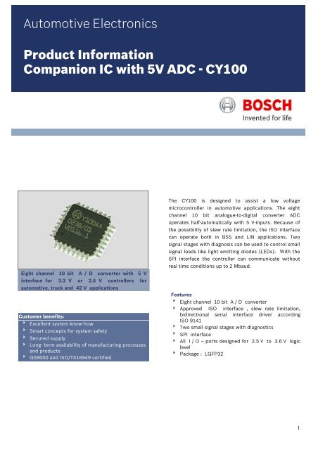
Automotive Electronics<br />
Companion Product Information IC with 5 V ADC<br />
CY100 Companion IC with 5V ADC - CY100<br />
Eight channel 10 bit A / D converter with 5 V<br />
interface for 3.3 V or 2.5 V controllers for<br />
automotive, truck <strong>and</strong> 42 V applications<br />
Customer benefits:<br />
Excellent system know-how<br />
Smart concepts for system safety<br />
Secured supply<br />
Long- term availability of manufacturing processes<br />
<strong>and</strong> products<br />
QS9000 <strong>and</strong> ISO/TS16949 certified<br />
The CY100 is designed to assist a low voltage<br />
microcontroller in automotive applications. The eight<br />
channel 10 bit analogue-to-digital converter ADC<br />
operates half-automatically with 5 V-inputs. Because of<br />
the possibility of slew rate limitation, the ISO interface<br />
can operate both in BSS <strong>and</strong> LIN applications. Two<br />
signal stages with diagnosis can be used to control small<br />
signal loads like light emitting diodes (LEDs). With the<br />
SPI interface the controller can communicate without<br />
real time conditions up to 2 Mbaud.<br />
Features<br />
Eight channel 10 bit A / D converter<br />
Approved ISO interface , slew rate limitation,<br />
bidirectional serial interface driver according<br />
ISO 9141<br />
Two small signal stages with diagnostics<br />
SPI interface<br />
All I / O – ports designed for 2.5 V to 3.6 V logic<br />
level<br />
Package : LQFP32<br />
1
Block diagram<br />
Pin description<br />
AN_IN0..7<br />
INT<br />
E1<br />
E2<br />
A2<br />
A1<br />
AREF GNDA VDD5A CLK VDD5<br />
AD Converter<br />
SPI<br />
(for diagnosis) Reset<br />
RST<br />
small signal<br />
stages<br />
-1<br />
2x<br />
Reset<br />
8 Channel<br />
+ Logic<br />
Application example<br />
Reset<br />
RAM<br />
Reset<br />
SPI-Interface<br />
ISO-Interface<br />
ISO9141<br />
TST GNDL GND2 VDDIO<br />
-1<br />
SI<br />
SO<br />
SCK<br />
SS<br />
UBREF<br />
UBat<br />
RX<br />
TX<br />
RT<br />
Pin Name Function<br />
16<br />
15<br />
14<br />
13<br />
RX<br />
TX<br />
RT<br />
UB_REF<br />
Receiver output driver ISO 9141<br />
Transmitter input driver ISO 9141<br />
Input/output driver ISO 9141<br />
UB-Reference for theISO 9141 receiver<br />
9<br />
10<br />
8<br />
7<br />
32<br />
31<br />
30<br />
29<br />
28<br />
27<br />
26<br />
25<br />
22<br />
23<br />
17<br />
19<br />
18<br />
20<br />
1<br />
2<br />
3<br />
12<br />
6<br />
21<br />
5<br />
11<br />
4<br />
24<br />
A1<br />
A2<br />
E1<br />
E2<br />
AN_IN0<br />
AN_IN1<br />
AN_IN2<br />
AN_IN3<br />
AN_IN4<br />
AN_IN5<br />
AN_IN6<br />
AN_IN7<br />
CLK<br />
INT<br />
SS<br />
SO<br />
SI<br />
SCK<br />
AREF<br />
VDD5A<br />
GNDA<br />
UBat<br />
VDD5<br />
VDDIO<br />
GND1<br />
GND2<br />
RST<br />
TST<br />
Output small signal stage 1<br />
Output small signal stage 2<br />
Input small signal stage 1<br />
Input small signal stage 2<br />
Analog input 0<br />
Analog input 1<br />
Analog input 2<br />
Analog input 3<br />
Analog input 4<br />
Analog input 5 (only half sample rate<br />
of the others channels )<br />
Analog input 6<br />
Analog input 7<br />
CLK-input for the A-to-D Converter<br />
( Necessary to enable the CY100 )<br />
Interrupt-Output for the A-to-D<br />
Converter<br />
SPI slave-select signal<br />
Slave-Out signal ( SPI data output )<br />
Slave-In signal ( SPI data input )<br />
SPI serial clock input<br />
Analog reference voltage for the ADC<br />
Analog supply voltage 5 V<br />
Analog ground<br />
UBat Pin for ESD protection<br />
5 V - digital supply<br />
3.3 V / 2.5 V - supply for IO<br />
Digital-ground mainly for ’on chip’<br />
digital modules<br />
Digital-ground mainly for ’on chip’<br />
power modules like ISO, KSA <strong>and</strong><br />
SPI<br />
Reset-input<br />
not used -> to be connected to ground<br />
VDD5<br />
AN_IN0<br />
GN DA<br />
VDD5<br />
Rin<br />
AN_IN3<br />
Cmax<br />
GNDA<br />
TESTM3<br />
GNDA<br />
INT<br />
Rmux<br />
Rmux<br />
Rmux<br />
Rmux<br />
Rmux<br />
Rmux<br />
Rmux<br />
Rmux<br />
MUX<br />
S&H<br />
Cs<br />
ADC (10 Bit; SAR)<br />
01 1011 0101<br />
AREF<br />
offset<br />
channel<br />
digital offset<br />
Rmux<br />
compensation<br />
R result register<br />
DSon offset<br />
reference<br />
for compensation<br />
RAM<br />
Bank0 Bank1<br />
Control<br />
internal bus<br />
ADC - SPI transfer<br />
register (BIOR)<br />
Maximum ratings<br />
Parameter Min Max Unit<br />
Maximum Voltage, RT<br />
Maximum Voltage, UBat, UB_REF<br />
Maximum Voltage, A1, A2<br />
Maximum Voltage, VDD5,<br />
VDD5A, AREF<br />
Maximum Voltage, VDDIO<br />
Maximum Voltage, AN_INx, CLK<br />
E1, E2, RST, SCK, SI, SS, TX<br />
-15<br />
-2<br />
-0.6<br />
-0.3<br />
-0.3<br />
-0.3<br />
-0.3<br />
60<br />
60<br />
60<br />
6<br />
4<br />
UVDD5<br />
+ 0.3<br />
UVDDIO<br />
V<br />
V<br />
V<br />
V<br />
V<br />
V<br />
V<br />
Maximum Voltage, INT, RX, SO<br />
+ 0.3<br />
Frequency operating range<br />
Maximum SPI transfer rate<br />
2.5 12<br />
2<br />
MHz<br />
MBd<br />
Operating temperature Tj<br />
Thermal resistance<br />
ESD HBM, MIL883D 3015<br />
100pF / 1.5kΩ<br />
A1, A2, RT<br />
All other pins<br />
-40 150<br />
60<br />
- 4<br />
- 2<br />
+ 4<br />
+ 2<br />
°C<br />
K/W<br />
kV<br />
kV<br />
f CCLK<br />
(= 2.5MHz or 3MHz)<br />
SPI<br />
f cycle<br />
T Testm3<br />
5000 or 6000)<br />
Divider 2<br />
(2500, 3000,<br />
Divider 1<br />
(1,2,3 or 4)<br />
CLK<br />
2
A/D Converter (ADC)<br />
Serial Interface / ISO Driver<br />
The CY100 uses a 10 Bit SAR (successive approximation<br />
register) Converter with S&H (sample <strong>and</strong> hold)<br />
element. The total error (gain, offset, non linearity) is<br />
less than 2 LSB <strong>and</strong> less than 4 LSB near ground or<br />
AREF. The CY100 has an internal offset compensation<br />
algorithmus. The conversion <strong>and</strong> sample time for each<br />
channel is faster than 125 us. The ADC is mixed to 8<br />
external input channels except channel 5, which is<br />
additional multiplexed with the internal channel for the<br />
CY100 offset compensation on chip.<br />
So a converting time of 1 ms of channel 0 to 4 <strong>and</strong> 6<br />
to 7 can reached, whereas channel 5 can be converted<br />
every 2 ms. All 8 channels are running in timed mode<br />
without jitter.<br />
The input voltage range is 0 V. 5.5 V. The input pins<br />
AN_INx are clamped to VDD5 <strong>and</strong> GND by an ESD<br />
protection diode. The ADC has a separate reference<br />
input pin AREF.<br />
After conversion of all 8 channels the results are<br />
storaged in the result RAM. After ending the conversion<br />
of channel 7 the output INT becomes active (low). This<br />
output can be used to trigger a microcontroller with<br />
interrupt or DMA request.<br />
Parameter Min Max Unit<br />
Input range<br />
Switched capacitance<br />
-0.3 UVDD5A<br />
+ 0.3<br />
20<br />
V<br />
pF<br />
Resolution for the input range<br />
Conversion time for each<br />
channel ( f=2,5 MHz )<br />
Maximum sample rate<br />
10<br />
122<br />
1<br />
Bit<br />
s<br />
kHz<br />
AREF = 5 V :<br />
Resolution, 0.1 V < AN_INx <<br />
4.9 V<br />
Resolution, AN_INx ≤ 100 mV<br />
Resolution, AN_INx ≥ 4.9 V<br />
VDD5<br />
AN_IN0<br />
GNDA<br />
VDD5<br />
AN_IN3<br />
Cmax<br />
TESTM3<br />
Rin<br />
GNDA<br />
GNDA<br />
Rmux<br />
Rmux<br />
Rmux<br />
Rmux<br />
Rmux<br />
Rmux<br />
Rmux<br />
Rmux<br />
MUX<br />
± 2<br />
± 4<br />
± 4<br />
S&H<br />
LSB<br />
LSB<br />
LSB<br />
Cs<br />
ADC (10 Bit; SAR)<br />
01 1011 0101<br />
AREF<br />
offset<br />
channel<br />
digital offset<br />
Rmux<br />
compensation<br />
R result register<br />
DSon offset<br />
reference<br />
for compensation<br />
RAM<br />
Bank0 Bank1<br />
Integrated in the CY100 is one bi-directional serial<br />
interface driver, enabling data transfer according to ISO<br />
9141. The driver can be used, for example, as the<br />
diagnosis interface, for an immobilizer or for a generator<br />
interface. If the interface is not used, the transmitter<br />
side can be deployed as a small-signal stage.<br />
The input/output pin RT is protected against destruction<br />
from ISO impulses 3a <strong>and</strong> 3b.<br />
TX<br />
RST<br />
RX<br />
Parameter Min Max Unit<br />
RT low level at IRT = 40 mA<br />
RT nominal output current<br />
RT off state input current<br />
RT slew rate limitation, negative<br />
edge, deactivatable<br />
-5<br />
1<br />
1.4<br />
50<br />
10<br />
3<br />
V<br />
mA<br />
A<br />
V/s<br />
RX1 low output voltage<br />
RX1 high output voltage<br />
TX1 low level<br />
TX1 high level<br />
VDDIO VDDIO<br />
other<br />
modules<br />
Reset signal<br />
Receiver<br />
shut off time /<br />
shut off filter time<br />
slew rate<br />
control<br />
Transmitter<br />
divider on/off<br />
UVDDIO<br />
– 0.4<br />
-0.3<br />
0.7 *<br />
UVDDIO<br />
SPI-Bits<br />
(SOT_EN, ISO_DLY)<br />
SPI-Bit (ISO_SRC)<br />
UB_REF<br />
UVDDIO<br />
0.3 *<br />
UVDDIO<br />
UVDD5 +<br />
0.3<br />
V<br />
V<br />
V<br />
V<br />
RT<br />
INT<br />
Control<br />
internal bus<br />
ADC - SPI transfer<br />
register (BIOR)<br />
f CCLK<br />
(= 2.5MHz or 3MHz)<br />
SPI<br />
f cycle<br />
T Testm3<br />
5000 or 6000)<br />
Divider 2<br />
(2500, 3000,<br />
Divider 1<br />
(1,2,3 or 4)<br />
CLK<br />
3
Small signal stags<br />
Two identical small-signal stages with open-drain<br />
outputs are integrated in the CY100. The output stages<br />
are mainly for digital outputs, for the control of “semiintelligent”<br />
actors (e.g. semi-conductor relays) <strong>and</strong> for<br />
driving LEDs.<br />
The inputs E1 <strong>and</strong> E2 are realized as comparators with<br />
VDDIO - dependent threshold. The inputs have pull-up<br />
current sources, so that in case of an open input, the<br />
output stages are disabled. The phase of the outputs is<br />
non-inverting.<br />
Parameter Min Max Unit<br />
A1, A2 maximum voltage<br />
A1, A2 nominal output current<br />
A1, A2 regulated short circuit<br />
current<br />
-0.6<br />
50<br />
60<br />
50<br />
120<br />
V<br />
mA<br />
mA<br />
A1, A2 on resistance<br />
Switching time E1 to A1,<br />
E2 to A2<br />
12<br />
2<br />
Ω<br />
µs<br />
The OL diagnosis can be disabled individually via the SPI<br />
interface for each output stage for applications, for<br />
which the diagnostic current can disturb (e.g. LEDs).<br />
Disable means, zero diagnostic current for OL <strong>and</strong><br />
deactivated error indication OL.<br />
The output stages are disabled (transistors switched<br />
off), when the reset signal on RST is active.<br />
VDDIO<br />
SPI-Bits<br />
diagnose<br />
SPI Interface<br />
The serial SPI interface establishes a communication link<br />
between CY100 <strong>and</strong> the systems microcontroller. The<br />
CY100 always operates in slave mode whereas the<br />
controller provides the master function. The maximum<br />
baud rate is 2 MBaud.<br />
Ex<br />
RST<br />
&<br />
Ax<br />
Applying an active slave select signal at SS CY100 is<br />
selected by the SPI master. SI is the slave in data input,<br />
SO the slave out data output. Via the serial clock input<br />
SCK the SPI clock is provided by the SPI master. In case<br />
of inactive slave select signal (high) or active reset the<br />
data output SO is high impedance (tistate).<br />
The transmit-function has to be enabled via SPI soft<br />
reset after an active RST (low). The open-drain outputs<br />
are current-limited, in addition the output voltage on Ax<br />
(x=1; 2) is monitored for plausibility. If the voltage at Ax<br />
still exceeds a certain defined threshold after switch on<br />
the output transistor <strong>and</strong> after a predefined time tvoff, a<br />
short- circuit to battery is detected <strong>and</strong> the stage is<br />
turned off.<br />
The first two bits of an instruction are used to realize an<br />
extended device-addressing. This gives the opportunity<br />
to operate up to 4 slave-devices sharing one common SS<br />
signal from the master-unit.<br />
configuration<br />
reg. (read / write)<br />
status registers<br />
(read only)<br />
The output stages can also be diagnosed. The error<br />
conditions short-circuit to battery (SCB), short-circuit to<br />
ground (SCG) <strong>and</strong> open-load (OL) are detected. Error<br />
detection is done selectively according to the output<br />
stage condition: OL <strong>and</strong> SCG are detected when the<br />
output stage is disabled; SCB is detected when the<br />
output stage is on. The errors OL, SCB <strong>and</strong> SCG are<br />
filtered.<br />
SS<br />
SCK<br />
SO<br />
SI<br />
SPI Shift Register<br />
SPI Control:<br />
State Machine<br />
ID registers<br />
(read only)<br />
ADC RAM<br />
(read / write)<br />
4
_<br />
+<br />
_<br />
+<br />
System application example<br />
Chipset<br />
Battery<br />
Sensor<br />
Sensor<br />
Sensor<br />
CAN<br />
ISO<br />
8x<br />
8<br />
CY320<br />
System Supply<br />
µC Supply<br />
Sensor Supply<br />
Watchdog<br />
Reset<br />
CAN Driver<br />
ISO Interface<br />
Sleep/Wake<br />
CY100<br />
µC<br />
e.g.<br />
Infineon<br />
TC1796<br />
A/D<br />
RAM<br />
CAN<br />
Peripherals<br />
FLASH<br />
CJ945<br />
18 Low Side<br />
Power Drivers<br />
6x 2A/70V<br />
6x 2A/45V<br />
2x 3A/45V<br />
4x 1A/45V<br />
CK240<br />
Ignition Drivers<br />
x<br />
x<br />
x<br />
x<br />
x<br />
x<br />
Fela<br />
Valves<br />
Relays<br />
Inductivities<br />
Resistors<br />
Lamps<br />
e.g.<br />
LEDs<br />
Fela<br />
2<br />
ISO<br />
8x 10 Bit A/D 5V<br />
Small Signal Out<br />
ISO Interface<br />
CY30<br />
RPM<br />
FLASH<br />
H-Bridge<br />
Concept<br />
CF173<br />
CAN Driver<br />
CAN<br />
CJ840<br />
Direct Injection<br />
SMD085<br />
Pressure Sensor<br />
CJ125<br />
λ-Sensor Control<br />
Contact<br />
Robert <strong>Bosch</strong> GmbH<br />
Sales <strong>Semiconductors</strong><br />
Postbox 13 42<br />
72703 Reutlingen<br />
Germany<br />
Tel.: +49 7121 35-2979<br />
Fax: +49 7121 35-2170<br />
Robert <strong>Bosch</strong> Corporation<br />
Component Sales<br />
38000 Hills Tech Drive<br />
Farmington Hills, MI 48331<br />
USA<br />
Tel.: +1 248 876-7441<br />
Fax: +1 248 848-2818<br />
Robert <strong>Bosch</strong> K.K.<br />
Component Sales<br />
9-1, Ushikubo 3-chome<br />
Tsuzuki-ku, Yokohama 224<br />
Japan<br />
Tel.: +81 45 9 12-83 01<br />
Fax: +81 45 9 12-95 73<br />
E-Mail: bosch.semiconductors@de.bosch.com<br />
Internet: www.bosch-semiconductors.de<br />
© 02/2006 All rights reserved by Robert <strong>Bosch</strong> GmbH including the right to file industrial property rights<br />
Robert <strong>Bosch</strong> GmbH retains the sole powers of distribution, such as reproduction, copying <strong>and</strong> distribution.<br />
For any use of products outside the released application, specified environments or installation conditions no warranty shall apply <strong>and</strong><br />
<strong>Bosch</strong> shall not be liable for such products or any damage caused by such products.<br />
5