Archive of SID
Archive of SID
Archive of SID

You also want an ePaper? Increase the reach of your titles
YUMPU automatically turns print PDFs into web optimized ePapers that Google loves.
S. Deepa and S. Rajapandian /IJE TRANSACTIONS C: Aspects Vol. 26, No. 3, (March 2013) 309-314 312<br />
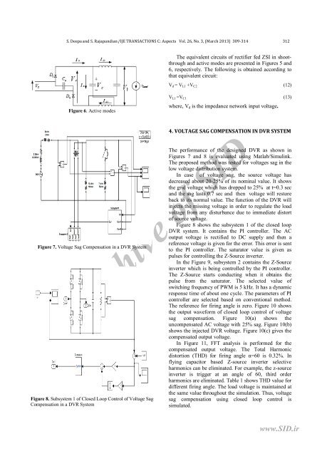
The equivalent circuits <strong>of</strong> rectifier fed ZSI in shootthrough<br />
and active modes are presented in Figures 5 and<br />
6, respectively. The following is obtained according to<br />
that equivalent circuit:<br />
V d = V L1 +V C2 (12)<br />
Figure 6. Active modes<br />
V L1 =V C1 (13)<br />
where, V d is the impedance network input voltage.<br />
Figure 7. Voltage Sag Compensation in a DVR System<br />
<strong>Archive</strong> <strong>of</strong> <strong>SID</strong><br />
Figure 8. Subsystem 1 <strong>of</strong> Closed Loop Control <strong>of</strong> Voltage Sag<br />
Compensation in a DVR System<br />
4. VOLTAGE SAG COMPENSATION IN DVR SYSTEM<br />
The performance <strong>of</strong> the designed DVR as shown in<br />
Figures 7 and 8 is evaluated using Matlab/Simulink.<br />
The proposed method was tested for voltages sag in the<br />
low voltage distribution system.<br />
In case <strong>of</strong> voltage sag, the source voltage has<br />
decreased about 20-25% <strong>of</strong> its nominal value. It shows<br />
the grid voltage which has dropped to 25% at t=0.3 sec<br />
and the sag lasts 0.7 sec and then voltage will restore<br />
back to its normal value. The function <strong>of</strong> the DVR will<br />
injects the missing voltage in order to regulate the load<br />
voltage from any disturbance due to immediate distort<br />
<strong>of</strong> source voltage.<br />
Figure 8 shows the subsystem 1 <strong>of</strong> the closed loop<br />
DVR system. It contains the PI controller. The AC<br />
output voltage is rectified to DC supply and then a<br />
reference voltage is given for the error. This error is sent<br />
to the PI controller. The saturator value is given as<br />
pulses for controlling the Z-Source inverter.<br />
In the Figure 9, subsystem 2 contains the Z-Source<br />
inverter which is being controlled by the PI controller.<br />
The Z-Source starts conducting when it obtains the<br />
pulse from the saturator. The selected value <strong>of</strong><br />
switching frequency <strong>of</strong> PWM is 5 kHz. It has a dynamic<br />
response time <strong>of</strong> about one cycle. The parameters <strong>of</strong> PI<br />
controller are selected based on conventional method.<br />
The reference for firing angle is zero. Figure 10 shows<br />
the output waveform <strong>of</strong> closed loop control <strong>of</strong> voltage<br />
sag compensation. Figure 10(a) shows the<br />
uncompensated AC voltage with 25% sag. Figure 10(b)<br />
shows the injected DVR voltage. Figure 10(c) gives the<br />
compensated output voltage.<br />
In Figure 11, FFT analysis is performed for the<br />
compensated output voltage. The Total Harmonic<br />
distortion (THD) for firing angle α=60 is 0.32%. In<br />
flying capacitor based Z-source inverter selective<br />
harmonics can be eliminated. For example, the z-source<br />
inverter is trigger at an angle <strong>of</strong> 60, third order<br />
harmonics are eliminated. Table 1 shows THD value for<br />
different firing angle. The load voltage is maintained at<br />
the same value throughout the simulation. Thus, voltage<br />
sag compensation using closed loop control is<br />
simulated.<br />
www.<strong>SID</strong>.ir