Carbon Nanomaterials (PDF)
Carbon Nanomaterials (PDF)
Carbon Nanomaterials (PDF)

Create successful ePaper yourself
Turn your PDF publications into a flip-book with our unique Google optimized e-Paper software.
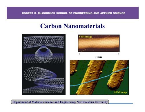
<strong>Carbon</strong> <strong>Nanomaterials</strong><br />
STM Image<br />
7 nm<br />
AFM Image<br />
Department of Materials Science and Engineering, Northwestern University
Fullerenes<br />
• C 60<br />
was established by mass spectrographic analysis by Kroto and Smalley in 1985<br />
• C 60<br />
is called a buckminsterfullerene or buckyball due to resemblance to geodesic<br />
domes designed and built by R. Buckminster Fuller<br />
G. Timp, Nanotechnology, Chapter 7<br />
Department of Materials Science and Engineering, Northwestern University
Endofullerenes<br />
• Endohedral doping of fullerenes leads to the formation of a dipole moment that<br />
influences solubility and other properties.<br />
G. Timp, Nanotechnology, Chapter 7<br />
Department of Materials Science and Engineering, Northwestern University
Electronic Structure of Molecular and Solid C 60<br />
G. Timp, Nanotechnology, Chapter 7<br />
Department of Materials Science and Engineering, Northwestern University
Dangling<br />
Bonds<br />
Single Molecule STM Spectroscopy of C 60<br />
3-D STM Topograph<br />
C 60<br />
70 Å x 70 Å<br />
Structure of C 60<br />
Spectroscopic variation among surface features<br />
Si<br />
dI/dV (A.U.)<br />
1.0<br />
0.8<br />
0.6<br />
0.4<br />
C 60<br />
Si Dangling Bond<br />
H-passivated Si<br />
LUMO peak<br />
Ge<br />
0.2<br />
0.0<br />
-2 -1 0 1 2<br />
Energy (eV)<br />
Calculated local density of states for Si(100)<br />
Department of Materials Science and Engineering, Northwestern University
Rolled Up From Graphene Sheets:<br />
<strong>Carbon</strong> Nanotubes<br />
G. Timp, Nanotechnology, Chapter 7<br />
Department of Materials Science and Engineering, Northwestern University
<strong>Carbon</strong> Nanotube Synthesis:<br />
<strong>Carbon</strong> Arc Discharge<br />
P. G. Collins and Ph. Avouris, Scientific American, 283, 62 (2000).<br />
Department of Materials Science and Engineering, Northwestern University
<strong>Carbon</strong> Nanotube Synthesis:<br />
Chemical Vapor Deposition<br />
P. G. Collins and Ph. Avouris, Scientific American, 283, 62 (2000).<br />
Department of Materials Science and Engineering, Northwestern University
<strong>Carbon</strong> Nanotube Synthesis:<br />
Laser Ablation<br />
P. G. Collins and Ph. Avouris, Scientific American, 283, 62 (2000).<br />
Department of Materials Science and Engineering, Northwestern University
Chirality of <strong>Carbon</strong> Nanotubes<br />
G. Timp, Nanotechnology, Chapter 7<br />
Department of Materials Science and Engineering, Northwestern University
Energy Band Diagrams of <strong>Carbon</strong> Nanotubes<br />
G. Timp, Nanotechnology, Chapter 7<br />
Department of Materials Science and Engineering, Northwestern University
Electrical Properties of Graphite<br />
P. G. Collins and Ph. Avouris, Scientific American, 283, 62 (2000).<br />
Department of Materials Science and Engineering, Northwestern University
Electrical Properties of Straight Nanotubes<br />
P. G. Collins and Ph. Avouris, Scientific American, 283, 62 (2000).<br />
Department of Materials Science and Engineering, Northwestern University
Electrical Properties of Twisted Nanotubes<br />
P. G. Collins and Ph. Avouris, Scientific American, 283, 62 (2000).<br />
Department of Materials Science and Engineering, Northwestern University
Bandgap of Semiconducting Nanotubes<br />
G. Timp, Nanotechnology, Chapter 7<br />
Department of Materials Science and Engineering, Northwestern University
Electrical Properties of MWNTs<br />
• MWNT bandgap is proportional to 1/d At room temperature,<br />
MWNTs behave like metals since d ~ 10 nm<br />
• Only the outermost shell carries current in an undamaged MWNT<br />
Department of Materials Science and Engineering, Northwestern University
Other Properties of SWNTs<br />
P. G. Collins and Ph. Avouris, Scientific American, 283, 62 (2000).<br />
Department of Materials Science and Engineering, Northwestern University
Other Properties of SWNTs<br />
P. G. Collins and Ph. Avouris, Scientific American, 283, 62 (2000).<br />
Department of Materials Science and Engineering, Northwestern University
Nanotubes as Interconnects<br />
P. G. Collins and Ph. Avouris, Scientific American, 283, 62 (2000).<br />
Department of Materials Science and Engineering, Northwestern University
Current Carrying Capacity of MWNTs<br />
Although a cross-sectional view of a MWNT shows several<br />
cylindrical shells, only the outermost shell carries current in<br />
an undamaged MWNT.<br />
Department of Materials Science and Engineering, Northwestern University
Representative MWNT I-V Curve:<br />
8<br />
Current density (x10 13 A/m 2 )<br />
6<br />
4<br />
2<br />
Maximum current density: 6.8 x 10 13 A/m 2<br />
Maximum electric field: 1.6 x 10 7 V/m<br />
0<br />
0<br />
2<br />
4<br />
6 8 10<br />
Electric field (x10 6 V/m)<br />
12<br />
14<br />
16<br />
Maximum current densities of potential interconnect materials:<br />
• Metals: 10 10 –10 12 A/m 2<br />
• Superconductors: J c ~ 10 12 A/m 2<br />
• MWNTs: >5×10 13 A/m 2<br />
Department of Materials Science and Engineering, Northwestern University
Electrically Stressed MWNTs<br />
Before Electrical Stress<br />
After Failure<br />
1 µm 2 AFM image<br />
1 µm 2 AFM image<br />
Experimental method: Monitor the current as a function of time<br />
while stressing the MWNT at a fixed voltage.<br />
Department of Materials Science and Engineering, Northwestern University
Multiwalled <strong>Carbon</strong> Nanotube Failure<br />
P. G. Collins, et al., Phys. Rev. Lett., 86, 3128 (2001).<br />
Department of Materials Science and Engineering, Northwestern University
Device Applications of Nanotube Junctions<br />
G. Timp, Nanotechnology, Chapter 7<br />
Department of Materials Science and Engineering, Northwestern University
Engineering <strong>Carbon</strong> Nanotubes<br />
Using Electrical Breakdown<br />
P. G. Collins, et al., Science, 292, 706 (2001).<br />
Department of Materials Science and Engineering, Northwestern University
Engineering <strong>Carbon</strong> Nanotubes<br />
Using Electrical Breakdown<br />
P. G. Collins, et al., Science, 292, 706 (2001).<br />
Department of Materials Science and Engineering, Northwestern University
Electronic Applications of SWNTs<br />
Field Effect Transistors<br />
Field Emission Displays<br />
P. G. Collins and Ph. Avouris, Scientific American, 283, 62 (2000).<br />
Department of Materials Science and Engineering, Northwestern University
Nanotube Complementary Logic<br />
V. Derycke, et al., Nano Letters, 1, 453 (2001).<br />
Department of Materials Science and Engineering, Northwestern University
Nanotube Complementary Logic<br />
V. Derycke, et al., Nano Letters, 1, 453 (2001).<br />
Department of Materials Science and Engineering, Northwestern University
Other Applications of Nanotubes<br />
P. G. Collins and Ph. Avouris, Scientific American, 283, 62 (2000).<br />
Department of Materials Science and Engineering, Northwestern University
Other Applications of Nanotubes<br />
P. G. Collins and Ph. Avouris, Scientific American, 283, 62 (2000).<br />
Department of Materials Science and Engineering, Northwestern University
Density of States<br />
In general, the density of states in d-dimensions is:<br />
⎛<br />
D(<br />
E)<br />
= ⎜<br />
⎝<br />
L ⎞<br />
⎟<br />
2π<br />
⎠<br />
d<br />
∫<br />
δ ( k(<br />
E)<br />
−k)<br />
dk<br />
∇ ( E)<br />
k<br />
d<br />
At band edges, ∇ ( E)<br />
= 0<br />
k<br />
van Hove singularities in the density of states<br />
T. W. Odom, et al., J. Phys. Chem. B, 104, 2794 (2000).<br />
Department of Materials Science and Engineering, Northwestern University
Nanotube 1-D Density of States<br />
The van Hove singularities assume different forms based on the<br />
dimensionality of the system:<br />
The 1-D nature of nanotubes leads to peaks in the density of states.<br />
T. W. Odom, et al., J. Phys. Chem. B, 104, 2794 (2000).<br />
Department of Materials Science and Engineering, Northwestern University
STM Measurements of Nanotube<br />
van Hove Singularities<br />
J. W. G. Wilder, et al., Nature, 391, 59 (1998).<br />
Department of Materials Science and Engineering, Northwestern University
Implications of van Hove Singularities<br />
for Nanotube Optical Properties<br />
S. M. Bachilo, et al., Science, 298, 2361 (2002).<br />
Department of Materials Science and Engineering, Northwestern University
Separating <strong>Carbon</strong> Nanotubes in Solution<br />
M. J. O’Connell, et al., Science, 297, 593 (2002).<br />
Department of Materials Science and Engineering, Northwestern University
Band Gap Absorption and Fluorescence from<br />
Individual Single-Walled <strong>Carbon</strong> Nanotubes<br />
M. J. O’Connell, et al., Science, 297, 593 (2002).<br />
Department of Materials Science and Engineering, Northwestern University
Excitation at the E 22 Transition<br />
M. J. O’Connell, et al., Science, 297, 593 (2002).<br />
Department of Materials Science and Engineering, Northwestern University
Structure-Assigned Optical Spectra<br />
S. M. Bachilo, et al., Science, 298, 2361 (2002).<br />
Department of Materials Science and Engineering, Northwestern University
Ambipolar <strong>Carbon</strong> Nanotube FET<br />
Fig. 1. (A) Schematic diagram of the<br />
ambipolar s-SWNT device structure. (B)<br />
Electrical characterization of a typical<br />
ambipolar device. A plot of the drain<br />
current versus Vg for a grounded source<br />
and a small drain potential of1Vis shown.<br />
The data indicate ambipolar behavior. (C)<br />
Plot of the drain current versus Vd for a<br />
grounded source and a gate potential of 5<br />
V for the device used in the optical<br />
measurements. The inset shows the data<br />
on a logarithmic scale. (D) Calculated<br />
band structure for carbon nanotube FET<br />
devices with Vd = 4 V and Vg halfway<br />
between the source and drain voltages.<br />
J. A. Misewich, et al., Science, 300, 783 (2003).<br />
Department of Materials Science and Engineering, Northwestern University
Infrared Emission from an Ambipolar Nanotube FET<br />
Fig. 2. Optical emission from an ambipolar<br />
carbon nanotube FET detected with an IR<br />
camera. The upper plane is a color-coded IR<br />
image of the carbon nanotube FET. The<br />
contact pads and thin wires leading to the<br />
carbon nanotube channel are shown in yellow.<br />
The lower plane is the surface plot of the IR<br />
emission image taken under conditions of<br />
simultaneous e– and h+ injection into the<br />
carbon nanotube. The emission was localized<br />
at the position of the carbon nanotube. (Inset)<br />
SEM showing the device structure in the<br />
region of the nanotube emitter.<br />
J. A. Misewich, et al., Science, 300, 783 (2003).<br />
Department of Materials Science and Engineering, Northwestern University
Characterization of Stimulated Emission<br />
from Encapsulated SWNTs<br />
M. S. Arnold, et al., Nano Letters, 3, 1549 (2003).<br />
Department of Materials Science and Engineering, Northwestern University
Filter<br />
Pulsed pump from Ti:sapphire<br />
laser (300 fs pulse width)<br />
Probe from CW<br />
fiber laser (λ=1053 nm)<br />
60dB<br />
ESA or oscilloscope<br />
Sample (stirred)<br />
Experimental setup<br />
Probe modulation [dBm]<br />
-20<br />
Pump & probe on<br />
-40<br />
Probe on<br />
-60<br />
-80<br />
Pump on<br />
-100<br />
75.72 75.74 75.76 75.78 75.80<br />
RF Frequency [MHz]<br />
Stimulated emission [mV]<br />
30<br />
20<br />
10<br />
0<br />
-10<br />
0 10 20 30 40 50<br />
Time [ns]<br />
Probe modulation in frequency domain<br />
Temporal response of probe modulation<br />
Department of Materials Science and Engineering, Northwestern University
Effect of Aggregation and pH<br />
• Aggregation of isolated nanotubes<br />
by lyophilization and re-suspension<br />
drastically reduces probe modulation<br />
intensity by a factor of 122.<br />
• Photobleaching disappears at acidic<br />
pH and is reversibly restored at<br />
neutral and basic pH, consistent with<br />
protonation of nanotube sidewalls at<br />
acidic pH.<br />
M. S. Arnold, et al., Nano Letters, 3, 1549 (2003).<br />
Department of Materials Science and Engineering, Northwestern University
Pump Spectral Dependence<br />
• The measured E 22 transition<br />
width of 65 meV is consistent with<br />
fast electron-electron scattering on<br />
the 300 fs time scale.<br />
• The feature near 1.4 eV is likely<br />
due to a Raman effect (the<br />
measured difference between<br />
pump and probe energies is ~<br />
1600 cm -1 , which matches the G-<br />
band Raman mode in SWNTs).<br />
M. S. Arnold, et al., Nano Letters, 3, 1549 (2003).<br />
Department of Materials Science and Engineering, Northwestern University
Probe Spectral Dependence<br />
• The probe modulation<br />
spectrum is slightly red-shifted<br />
from the absorbance spectrum<br />
by 45 cm -1 .<br />
• From a Lorentzian fit, the<br />
width of the E 11 transition is<br />
only 10 meV compared with 65<br />
meV as measured for the E 22<br />
transition.<br />
M. S. Arnold, et al., Nano Letters, 3, 1549 (2003).<br />
Department of Materials Science and Engineering, Northwestern University
Polarization Dependence<br />
Co-polarized pump and probe lead to greater photobleaching than<br />
cross-polarized as expected for a 1-D system.<br />
M. S. Arnold, et al., Nano Letters, 3, 1549 (2003).<br />
Department of Materials Science and Engineering, Northwestern University
Pump Saturation Effects<br />
• At low pump intensities below 10<br />
W/cm 2 , linear behavior is observed.<br />
• Saturation of the probe modulation<br />
is consistent with:<br />
‣ Increased multi-particle Auger<br />
recombination for large carrier<br />
densities.<br />
‣ Exciton-exciton annihilation<br />
effects.<br />
‣ Saturation and filling of a finite<br />
number of states.<br />
M. S. Arnold, et al., Nano Letters, 3, 1549 (2003).<br />
Department of Materials Science and Engineering, Northwestern University
Probe Saturation Effects<br />
• x S corresponds to the probe intensity<br />
for which the rate of stimulated<br />
recombination is equal to the intrinsic<br />
rate of recombination.<br />
•An increase in x s at large pump<br />
intensities is consistent with an increase<br />
in the effective interband recombination<br />
rate due to enhanced Auger<br />
recombination for large carrier densities.<br />
M. S. Arnold, et al., Nano Letters, 3, 1549 (2003).<br />
Department of Materials Science and Engineering, Northwestern University
Degenerate Pump-Probe Measurements<br />
Normalized modulation<br />
1.0<br />
0.8<br />
0.6<br />
0.4<br />
0.2<br />
Decay<br />
E 11<br />
E 22<br />
Degenerate pump-probe<br />
optical setup.<br />
0.0<br />
0<br />
40<br />
80<br />
delay (ps)<br />
120<br />
160<br />
Time-resolved relaxation at E 11 (975 nm)<br />
and E 22 (740 nm) optical transitions.<br />
Department of Materials Science and Engineering, Northwestern University
Temporal Relaxation at E 11<br />
Semi-log relaxation at E 11 (975 nm)<br />
Department of Materials Science and Engineering, Northwestern University
An Estimate of the Optical Gain<br />
~ 10%<br />
instantaneous<br />
decrease in<br />
absorption<br />
To reach optical<br />
transparency,<br />
SWNTs need to<br />
be separated<br />
by electronic<br />
bandstructure<br />
Department of Materials Science and Engineering, Northwestern University
DNA Encapsulated SWNTs<br />
M. Zheng, et al., Nature Mat., 2, 338 (2003). M. Zheng, et al., Science, 302, 1545 (2003).<br />
Department of Materials Science and Engineering, Northwestern University
SPM of DNA Encapsulated<br />
SWNTs on Silicon Surfaces<br />
Ambient AFM of ssDNA-NT on Si(111)-1x1:H<br />
UHV STM of ssDNA-NT on Si(100)-2x1:H<br />
Pitch ~12 nm<br />
Pitch ~12 nm<br />
Atomic force microscopy, scanning tunneling microscopy<br />
Department of Materials Science and Engineering, Northwestern University
Optical Absorption Spectra for<br />
DNA Encapsulated SWNTs<br />
Optical absorbance<br />
spectrum:<br />
Department of Materials Science and Engineering, Northwestern University
Density of DNA Encapsulated SWNTs<br />
Density of SWNTs in vacuum:<br />
ρ NT<br />
:=<br />
4 ρ s<br />
D<br />
Density of DNA encapsulated SWNTs:<br />
ρ s<br />
π D +<br />
ρ NT<br />
:=<br />
ρ s<br />
= areal density of graphite = 7.66×10 -8 g/cm 2<br />
ρ ext<br />
= volume density of hydrated DNA in iodixanol = 1.12 g/cm 3<br />
ρ π ⎛ ⎛<br />
ext ⎝ ⎜ ⎜<br />
⎝<br />
π ⎛ ⎝ ⎜<br />
D<br />
2<br />
D<br />
2<br />
+ t<br />
⎞<br />
⎟<br />
⎠<br />
+ t<br />
⎞<br />
⎟<br />
⎠<br />
2<br />
2<br />
−<br />
D 2<br />
4<br />
⎞<br />
⎟<br />
⎠<br />
M. S. Arnold, et al., Nano Letters, 5, 713 (2005).<br />
Department of Materials Science and Engineering, Northwestern University
Density Gradient Centrifugation of<br />
DNA Encapsulated SWNTs<br />
Density of DNA encapsulated SWNTs:<br />
1.11 – 1.17 g/cm 3<br />
→ DNA hydration layer thickness of 2 – 3 nm<br />
M. S. Arnold, et al., Nano Letters, 5, 713 (2005).<br />
Department of Materials Science and Engineering, Northwestern University
Separation of DNA Encapsulated<br />
SWNTs by Diameter<br />
M. S. Arnold, et al., Nano Letters, 5, 713 (2005).<br />
Department of Materials Science and Engineering, Northwestern University
Correlating Diameter and Density<br />
• Density of DNA encapsulated SWNTs increases with increasing diameter.<br />
• Separation is most effective at small diameters.<br />
M. S. Arnold, et al., Nano Letters, 5, 713 (2005).<br />
Department of Materials Science and Engineering, Northwestern University