SP4412A Electroluminescent Lamp Driver - Datasheet Catalog
SP4412A Electroluminescent Lamp Driver - Datasheet Catalog
SP4412A Electroluminescent Lamp Driver - Datasheet Catalog

You also want an ePaper? Increase the reach of your titles
YUMPU automatically turns print PDFs into web optimized ePapers that Google loves.
®<br />
<strong>SP4412A</strong><br />
■ 2.2 V- 3.6 V Battery Operation<br />
■ 50 nA Maximum Standby Current<br />
(10 nA typical)<br />
■ High Voltage Output Typical 160 V PP<br />
■ External Oscillator Required<br />
■ Enable Control Pin<br />
APPLICATIONS<br />
■ Watches<br />
■ Pagers<br />
■ Backlit LCD Displays<br />
<strong>Electroluminescent</strong> <strong>Lamp</strong> <strong>Driver</strong><br />
DESCRIPTION<br />
The <strong>SP4412A</strong> is a high voltage output DC-AC converter that can operate from a 2.2V-3.6V<br />
power supply. The <strong>SP4412A</strong> is capable of supplying up to 250 V PP<br />
signals, making it ideal<br />
for driving small electroluminescent lamps. The device features 10 nA (typical) standby<br />
current, for use in low power portable products. An inductor is used to generate the high<br />
voltage, and an external oscillator is needed as a clock source. The <strong>SP4412A</strong> is offered in<br />
an 8-pin narrow SOIC package or an 8-pin µSOIC package. For delivery in die form, please<br />
consult the factory.<br />
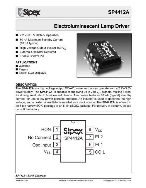
HON<br />
1<br />
8<br />
V DD<br />
No Connect<br />
2<br />
<strong>SP4412A</strong><br />
7<br />
EL2<br />
Osc Input<br />
3<br />
6<br />
EL1<br />
V SS<br />
4<br />
5<br />
COIL<br />
<strong>SP4412A</strong> Block Diagram<br />
<strong>SP4412A</strong>DS/12 <strong>SP4412A</strong>CN <strong>Electroluminescent</strong> <strong>Lamp</strong> <strong>Driver</strong> © Copyright 2000 Sipex Corporation<br />
1
ABSOLUTE MAXIMUM RATINGS<br />
These are stress ratings only and functional operation of the device at<br />
these ratings or any other above those indicated in the operation sections<br />
of the specifications below is not implied. Exposure to absolute maximum<br />
rating conditions for extended periods of time may affect reliability.<br />
V DD<br />
..................................................................................................5.0 V<br />
Input Voltages/Currents<br />
HON (pin 1).........................................-0.5V to (V DD<br />
+0.5V)<br />
COIL (pin 3)..............................................................60mA<br />
<strong>Lamp</strong> Outputs...............................................................................250V PP<br />
Storage Temperature.....................................................-65˚C to +150˚C<br />
The information furnished herein by Sipex has been carefully reviewed<br />
for accuracy and reliability. Its application or use, however, is solely the<br />
responsibility of the user. No responsibility for the use of this<br />
information is assumed by Sipex, and this information shall not explicitly<br />
or implicitly become part of the terms and conditions of any subsequent<br />
sales agreement with Sipex. Specifications are subject to change<br />
without prior notice. By the sale or transfer of this information, Sipex<br />
assumes no responsibility for any infringement of patents or other rights<br />
of third parties which may result from its use. No license or other<br />
proprietary rights are granted by implication or otherwise under any<br />
patent or patent rights of Sipex Corporation.<br />
Power Dissipation Per Package<br />
8-pin NSOIC (derate 6.14mW o C above +70 o C)...................................500mW<br />
8-pin µSOIC (derate 4.85mW o C above +70 o C)....................................390mW<br />
SPECIFICATIONS<br />
T= 25°C; V DD<br />
= 3.0V; <strong>Lamp</strong> Capacitance = 2000pF; Coil = 30 mH at 125 Ohms; External Oscillator = 32768Hz (unless otherwise noted).<br />
P ARAMETER<br />
M IN.<br />
T YP.<br />
MAX.<br />
UNITS<br />
CONDITIONS<br />
Supply<br />
Voltage,<br />
V<br />
. 2<br />
DD<br />
2 3.<br />
0 3.<br />
6 V<br />
Supply<br />
Current, I + I<br />
COIL<br />
DD<br />
5 2.<br />
0 mA<br />
V HON<br />
V<br />
= DD<br />
=3V<br />
Coil<br />
Voltage,<br />
V<br />
COIL<br />
V DD<br />
. 6<br />
3 V<br />
HON Input<br />
Voltage, VHON<br />
LOW:<br />
EL off<br />
HIGH: EL on<br />
-0.25<br />
V DD<br />
-0.25<br />
0<br />
V DD<br />
0.25V<br />
V DD<br />
+0.25<br />
HON Current, EL on<br />
1 10<br />
100<br />
µA<br />
Shutdown<br />
Current,<br />
INDUCTOR DRIVE<br />
I = I + I<br />
SD<br />
COIL<br />
DD<br />
0<br />
1 50<br />
nA<br />
V HON<br />
=0V<br />
V<br />
Coil<br />
Frequency,<br />
f = f 32<br />
COIL<br />
LAMP<br />
x 8192<br />
Hz<br />
Input Oscillator=32768Hz<br />
Coil<br />
Duty Cycle<br />
75<br />
%<br />
Peak<br />
Coil Current,<br />
EL LAMP OUTPUT<br />
I<br />
0<br />
PK-COIL<br />
6 m A Guaranteed by design.<br />
EL<br />
<strong>Lamp</strong> Frequency,<br />
f<br />
56<br />
LAMP<br />
2 Hz<br />
Input Oscillator=32768Hz<br />
Peak<br />
to Peak Output Voltage<br />
120<br />
160<br />
V PP<br />
BONDING DIAGRAM<br />
V SS<br />
Coil<br />
1143<br />
(45)<br />
Y<br />
(0,0)<br />
Clk.<br />
<strong>Lamp</strong> 2 <strong>Lamp</strong> 1<br />
X<br />
1397<br />
(55)<br />
HON<br />
V DD<br />
Measured from center of Pads.<br />
PIN X Y<br />
CLK 218.5 555.5<br />
HON 418.5 555.5<br />
V DD<br />
418.5 339.5<br />
EL2 -178.0 -555.5<br />
EL1 95.5 -555.5<br />
COIL -416.0 -555.5<br />
V SS -416.0 219.0<br />
NOTES:<br />
1. Dimensions are in microns unless otherwise noted (mils)<br />
2. Bonding pads are 125 x 125 microns typical<br />
3. Outside dimensions are maximum including scribe area<br />
4. Die thickness is 15 mils +/- 1<br />
5. Pad center coordinates are relative to the die center.<br />
<strong>SP4412A</strong>DS/12 <strong>SP4412A</strong>CN <strong>Electroluminescent</strong> <strong>Lamp</strong> <strong>Driver</strong> © Copyright 2000 Sipex Corporation<br />
2
PIN DESCRIPTION<br />
1<br />
2<br />
3<br />
4<br />
<strong>SP4412A</strong>CN<br />
8<br />
7<br />
6<br />
5<br />
Pin 1 – HON- Enable for driver operation,<br />
high = active; low = inactive.<br />
Pin 2 – NC<br />
Pin 3 – Oscillator clock input<br />
Pin 4 – V SS<br />
- Power supply common, connect to<br />
ground.<br />
Pin 5 – Coil - Coil input, connect coil from V DD<br />
to Pin 3.<br />
Pin 6 – <strong>Lamp</strong>- <strong>Lamp</strong> driver output1, connect to<br />
EL lamp.<br />
Pin 7 – <strong>Lamp</strong>- <strong>Lamp</strong> driver output2, connect to<br />
EL lamp.<br />
Pin 8 – V DD<br />
- Positive supply.<br />
THEORY OF OPERATION<br />
The <strong>SP4412A</strong> is made up of three basic circuit<br />
elements, a divider chain, a coil, and a switched<br />
H-bridge network. The countdown chain<br />
provides the circuit with a clock source used to<br />
control the charge and discharge phases for the<br />
coil and lamp. An external oscillator is required<br />
and is delivered to pin 3 of the SO-8 package or<br />
to the "Osc in" pad of the bare die. The chart on<br />
page 6 shows the effect of variations in coil<br />
values used. If a clock frequency other than<br />
32kHz is used, the output of the driver as well as<br />
the amount of current used, will be effected.<br />
The suggested oscillator frequency is 32,768Hz.<br />
This clock frequency is internally divided to<br />
create two internal control signals, f COIL<br />
and<br />
f LAMP<br />
. The output is internally divided down by<br />
7 flip flops; therefore, a 32,768Hz signal will be<br />
divided into the following frequencies; 32, 16,<br />
8, 4, 2, 1, 0.5 and 0.25kHz. The second flip flop<br />
output (8 kHz) is used to drive the coil (see<br />
figure 2 on page 7) and the seventh flip flop<br />
output (256 Hz) is used to drive the lamp.<br />
Although the oscillator frequency can be varied<br />
to optimize the lamp output, the ratio of f COIL<br />
/<br />
f LAMP<br />
will always equal 32.<br />
V DD<br />
V BATTERY or V DD<br />
30 mH at 125Ω<br />
8<br />
V DD<br />
1<br />
HON<br />
5<br />
Coil<br />
External<br />
Clock<br />
3<br />
Clock<br />
Divider<br />
Chain<br />
f COIL<br />
f LAMP<br />
FF1<br />
FF2<br />
Q<br />
Q<br />
f LAMP<br />
2<br />
NC<br />
V SS<br />
4<br />
EL1<br />
6<br />
EL2<br />
7<br />
EL <strong>Lamp</strong><br />
<strong>SP4412A</strong> Schematic<br />
<strong>SP4412A</strong>DS/12 <strong>SP4412A</strong>CN <strong>Electroluminescent</strong> <strong>Lamp</strong> <strong>Driver</strong> © Copyright 2000 Sipex Corporation<br />
3
The external clock should have a 50% duty<br />
cycle and range from V DD<br />
-1V to ground. The<br />
maximum external clock frequency is 128 kHz.<br />
The coil is an external component connected<br />
from V BATTERY<br />
to pin 5 of the <strong>SP4412A</strong>. Energy<br />
is developed in the coil according to the equation<br />
E L<br />
=1/2LI 2 where the current I is defined as<br />
I=(V BATTERY<br />
-IR-V OL<br />
)/R T<br />
. In order to maximize<br />
the energy produced by the coil, V BATTERY<br />
should<br />
represent the largest voltage in the system (up to<br />
a maximum of 3.6 v); V BATTERY<br />
= 3.0 VDC with<br />
a 35mH/125Ω coil is a typical example. It is not<br />
necessary that V DD<br />
=V BATTERY<br />
. The coil operation<br />
is a function of the core material and winding<br />
used -- performance variances may be noticeable<br />
from different coil suppliers even though the<br />
values are the same. The Sipex <strong>SP4412A</strong> is<br />
final tested using a 35 mH/135 ohm coil. For<br />
suggested coil sources see page 8.<br />
The f COIL<br />
signal controls a switch that connects<br />
the end of the coil at pin 5 to ground or to open<br />
circuit. The f COIL<br />
signal is a 94% duty cycle<br />
square wave, switching at 1/4 the oscillator<br />
frequency, (for a 32 kHz oscillator f COIL<br />
is 8<br />
kHz). During the time when the f COIL<br />
signal is<br />
high, the coil is connected from V BATTERY<br />
to<br />
ground and a charged magnetic field is created<br />
in the coil. During the low part of f COIL<br />
, the<br />
ground connection is switched open, the field<br />
collapses, and the energy in the inductor is forced<br />
to flow toward the high voltage H-bridge<br />
switches. f COIL<br />
will send 16 of these charge<br />
pulses to the lamp, each pulse increases the<br />
voltage drop across the lamp in discrete steps. As<br />
the voltage potential approaches its maximum,<br />
the steps become shorter (see figure 1 on page 7).<br />
The H-bridge consists of two SCR structures that<br />
act as high voltage switches. These two switches<br />
control the polarity of how the lamp is charged.<br />
The SCR switches are controlled by the f LAMP<br />
signal which is the oscillator frequency divided<br />
by 128. For a 32kHz oscillator, f LAMP<br />
= 250Hz.<br />
When the energy from the coil is released, a high<br />
voltage spike is created triggering the SCR<br />
switches. The direction of current flow is<br />
determined by which SCR is enabled. One full<br />
cycle of the H-bridge will create 16 voltage steps<br />
from ground to 80V (typical) on pins 6 and 7<br />
which are 180 degrees out of phase with each<br />
other (see figure 3 on page 7). A differential view<br />
of the outputs is shown in figure 4 on page 7.<br />
ELECTROLUMINESCENT TECHNOLOGY<br />
What is electroluminescence?<br />
An EL lamp is basically a strip of plastic that is<br />
coated with a phosphorous material which emits<br />
light (fluoresces) when a high voltage (>40V)<br />
which was first applied across it, is removed or<br />
reversed. Long periods of DC voltages applied to<br />
the material tend to breakdown the material and<br />
reduce its lifetime. With these considerations in<br />
mind, the ideal signal to drive an EL lamp is a<br />
high voltage sine wave. Traditional approaches<br />
to achieving this type of waveform included<br />
discrete circuits incorporating a transformer,<br />
transistors, and several resistors and capacitors.<br />
This approach is large and bulky, and cannot be<br />
implemented in most hand held equipment. Sipex<br />
now offers low power single chip driver circuits<br />
specifically designed to drive small to medium<br />
sized electroluminescent panels. All that is<br />
required is an external inductor and an external<br />
clock signal.<br />
1<br />
HON<br />
V DD<br />
8<br />
3 VDC<br />
2<br />
<strong>Lamp</strong><br />
7<br />
3<br />
Clk<br />
<strong>Lamp</strong><br />
6<br />
4 Coil 5<br />
V SS<br />
Coil<br />
LAMP<br />
32-64 Khz<br />
30 mH 125 ohm Coil<br />
Typical <strong>SP4412A</strong>CN Application Circuit<br />
<strong>SP4412A</strong>DS/12 <strong>SP4412A</strong>CN <strong>Electroluminescent</strong> <strong>Lamp</strong> <strong>Driver</strong> © Copyright 2000 Sipex Corporation<br />
4
<strong>Electroluminescent</strong> backlighting is ideal when<br />
used with LCD displays, keypads, or other<br />
backlit readouts. Its main use is to illuminate<br />
displays in dim to dark conditions for momentary<br />
periods of time. EL lamps typically consume less<br />
current than LEDs or incandescent bulbs making<br />
them ideal for battery powered products. Also,<br />
EL lamps are able to evenly light an area without<br />
creating "hot spots" in the display.<br />
The amount of light emitted is a function of the<br />
voltage applied to the lamp, the frequency at<br />
which it is applied, the lamp material used and<br />
its size, and lastly, the inductor used. There<br />
are many variables which can be optimized<br />
for specific applications. Sipex supplies<br />
characterization charts to aid the designer<br />
in selecting the optimum circuit configuration<br />
(see page 6).<br />
<strong>SP4412A</strong>DS/12 <strong>SP4412A</strong>CN <strong>Electroluminescent</strong> <strong>Lamp</strong> <strong>Driver</strong> © Copyright 2000 Sipex Corporation<br />
5
The following performance curves are intended to give the designer a relative scale from which to optimize<br />
specific applications. Absolute measurements may vary depending upon the brand of components chosen.<br />
FtL. vs Brightness <strong>Lamp</strong> Sizes vs. <strong>Lamp</strong> for Size various as a function Coils of coil inductance and impedance<br />
6<br />
5<br />
25mH 138Ω Ω @@ 3.03.0vdc<br />
VDC<br />
25mH 138Ω Ω @@ 2.22.2vdc<br />
VDC<br />
15mH 70Ω Ω @@ 3.03.0vdc<br />
VDC<br />
Footlamberts Brightness (FtL) (FtL)<br />
4<br />
3<br />
2<br />
1<br />
0<br />
15 15mH 70Ω Ω @@ 2.20 2.20vdc VDC<br />
20 20mH 70Ω Ω @@ 3.03.0vdc<br />
VDC<br />
(CTC)<br />
(CTC)<br />
20 25mH mH 70Ω Ω @@ 2.22.2vdc<br />
VDC<br />
(CTC)<br />
(CTC)<br />
29mH 62Ω Ω @ 3.0 3.0 VDC vdc<br />
(SK121)<br />
(Sk121)<br />
29mH mH 62Ω Ω @@ 2.2 2.2vdc VDC<br />
(SK121)<br />
(Sk 121)<br />
0.5 0.75 1 1.5 2<br />
<strong>Lamp</strong> lamp Sizes (sq. in in.) sq. in.<br />
<strong>SP4412A</strong>DS/12 <strong>SP4412A</strong>CN <strong>Electroluminescent</strong> <strong>Lamp</strong> <strong>Driver</strong> © Copyright 2000 Sipex Corporation<br />
6
V PEAK =80V (typical)<br />
EL1 output; 16 charge steps per half cycle<br />
Figure 1. EL output voltage in discrete steps at EL1 output<br />
16 coil pulses per half cycle; 94% duty cycle.<br />
Figure 2. Voltage pulses released from the coil to the EL driver circuitry<br />
EL1 Output<br />
-EL2 Output<br />
Figure 3. EL voltage waveforms from the EL1 and EL2 outputs<br />
EL1 Output<br />
V PP =160V<br />
(typical)<br />
-EL2 Output<br />
Differential representation EL 12 .<br />
Figure 4. EL differential output waveform of the EL1 and EL2 outputs<br />
<strong>SP4412A</strong>DS/12 <strong>SP4412A</strong>CN <strong>Electroluminescent</strong> <strong>Lamp</strong> <strong>Driver</strong> © Copyright 2000 Sipex Corporation<br />
7
HITACHI METALS Ltd.<br />
Kishimoto Bldg.<br />
2-1, Marunouchi 2-Chome,<br />
Chiyoda-Ku, Tokyo Japan<br />
Phone: 3-3284-4936<br />
Fax: 3-3287-1945<br />
Mr. Noboru Abe<br />
Spec.-<br />
9 mH ±30% 42 ohm (Max)<br />
Model: MD 735L902B<br />
Singapore<br />
Mr Stan kaiko,<br />
Mr. Hiroshi Kai<br />
Ph: 65-222-3077<br />
Fax: 65-222-5232<br />
Hong Kong<br />
Mr Mori Ota<br />
Ph: 852-2724-4183<br />
Fax: 852-2311-2095<br />
San Jose, CA<br />
Mr. Kent Oda<br />
Ph: 1-800-309-1803<br />
Fx: 408 436-9601<br />
6.8<br />
±0.3<br />
3.3<br />
±0.3<br />
7.0 ±0.5<br />
6.0 ±0.3<br />
(All Dimensions in mm)<br />
Sankyo Shoji Co. (HK)<br />
RM 28, 9/il Thriving Ind. Centre<br />
Tsuen Wan, N.T.<br />
Hong Kong<br />
8.1<br />
±0.2<br />
Phone: 8522 414 9268<br />
Fax: 8522 413 6040<br />
Contact: Mr. K.M. Chang<br />
Inductance: 29mH ±20 %<br />
Resistance: 62 Ohms ±10% @ 25˚C<br />
Part Number SK-121 1.5 3.3<br />
(All Dimensions in mm) ±0.2<br />
11.0<br />
±0.2<br />
Sankyo Shoji Co. (HK)<br />
RM 28, 9/il Thriving Ind. Centre<br />
Tsuen Wan, N.T.<br />
Hong Kong<br />
Phone: 8522 414 9268<br />
Fax: 8522 413 6040<br />
Contact: Mr. K.M. Chang<br />
Inductance: 65mH ±15mH<br />
Resistance: 270 Ohms ±15% @ 25˚C<br />
Part Number SK-80<br />
3.6 5.6 Max.<br />
0.8<br />
2.4<br />
(All Dimensions in mm)<br />
CTC Coils LTD (HK)<br />
Flat L-M 14 Fl, Haribest Ind'l Bldg.<br />
45-47 Au Pul Wan Street<br />
Fo Tan Shatin. N.T., Hong Kong<br />
Phone: 85 2695 4889<br />
Fax: 85 2695 1842<br />
Contact: Alfred Wong cc Marine Au<br />
Inductance: 20 mH ±10%<br />
Resistance: 65 Ohms Max<br />
Model Number: CH5070AS-203K-006<br />
Sipex No. S51208-M-1021-Sipex<br />
2.5<br />
6.5 Max 9.0 Max<br />
25 ± 2.0<br />
(All dimensions in mm)<br />
Mark Technology: North American stocking distributor for Sankyo and CTC<br />
Phone: 905-891-0165 FAX: 905-891-8534.<br />
EL polarizers/transflector<br />
manufacturers<br />
Nitto Denko<br />
Yoshi Shinozuka<br />
56 Nicholson Lane<br />
San Jose, CA. 432-5480<br />
Top Polarizer- NPF F1205DU<br />
Bottom - NPF F4225<br />
or (F4205) P3 w/transflector<br />
Transflector Material<br />
Astra Products<br />
Mark Bogin<br />
P.O. Box 479<br />
Baldwin, NJ 11510<br />
Phone (516)-223-7500<br />
Fax (516)-868-2371<br />
EL <strong>Lamp</strong> manufacturers<br />
Leading Edge Ind. Inc.<br />
11578 Encore Circle<br />
Minnetonka, MN 55343<br />
Phone 1-800-845-6992<br />
Midori Mark Ltd.<br />
1-5 Komagata 2-Chome<br />
Taita-Ku 111-0043 Japan<br />
Phone: 81-03-3848-2011<br />
Luminescent Systems inc. (LSI)<br />
4 Lucent Drive<br />
Lebanon, NH. 03766<br />
Phone: (603) 643-7766<br />
Fax: (603) 643-5947<br />
NEC Corporation<br />
Yumi Saskai<br />
7-1, Shiba 5 Chome, Minato-ku,<br />
Tokyo 108-01, Japan<br />
Phone: (03) 3798-9572<br />
Fax: (03) 3798-6134<br />
Seiko Precision<br />
Shuzo Abe<br />
1-1, Taihei 4-Chome,<br />
Sumida-ku, Tokyo, 139 Japan<br />
Phone: (03) 5610-7089<br />
Fax: (03) 5610-7177<br />
Gunze Electronics<br />
2113 Wells Branch Parkway<br />
Austin, TX 78728<br />
Phone: (512) 752-1299<br />
Fax: (512) 252-1181<br />
<strong>SP4412A</strong>DS/12 <strong>SP4412A</strong>CN <strong>Electroluminescent</strong> <strong>Lamp</strong> <strong>Driver</strong> © Copyright 2000 Sipex Corporation<br />
8
All package dimensions in inches<br />
8-pin NSOIC<br />
8-pin µSOIC<br />
0.0256<br />
BSC<br />
12.0˚<br />
±4˚<br />
0.012<br />
±0.003<br />
0.008<br />
0.189/0.197<br />
0.0965<br />
±0.003<br />
<strong>SP4412A</strong>CU<br />
0.118<br />
±0.002<br />
0.16<br />
±0.003<br />
R .003<br />
0˚ - 6˚<br />
0.006<br />
±0.006<br />
0.006<br />
±0.006<br />
0.150/0.157<br />
<strong>SP4412A</strong>CN<br />
0.228/0.244<br />
0.053/0.069<br />
0.020<br />
0.020<br />
12.0˚<br />
±4˚ 0.01<br />
0.0215<br />
±0.006<br />
0.037<br />
Ref<br />
3.0˚<br />
±3˚<br />
1<br />
2<br />
1<br />
0.014/0.019<br />
0.050 BSC<br />
0.116<br />
±0.004<br />
0.034<br />
±0.002<br />
0.040<br />
±0.002<br />
0.116<br />
±0.004<br />
0.013<br />
±0.005<br />
0.118<br />
±0.002<br />
0.004<br />
±0.002<br />
0.118<br />
±0.004<br />
95 <strong>SP4412A</strong>CN per tube, no minimum quantity<br />
50 <strong>SP4412A</strong>CU per tube<br />
P<br />
W<br />
NSOIC-8 13" reels: P=8mm, W=12mm<br />
µSOIC-8 13" reels: P=8mm, W=12mm<br />
Minimum qty per reel Standard qty per reel Maximum qty per reel<br />
500 2500 3000<br />
<strong>SP4412A</strong>DS/12 <strong>SP4412A</strong>CN <strong>Electroluminescent</strong> <strong>Lamp</strong> <strong>Driver</strong> © Copyright 2000 Sipex Corporation<br />
9
ORDERING INFORMATION<br />
Model Temperature Range Package Type<br />
<strong>SP4412A</strong>CN . ........................................... 0˚C to +70˚C ........................................... 8-Pin NSOIC<br />
<strong>SP4412A</strong>CU ............................................. 0˚C to +70˚C ........................................... 8-Pin µSOIC<br />
<strong>SP4412A</strong>CX ............................................. 0˚C to +70˚C .......................................................... Die<br />
Please consult the factory for pricing and availability on a Tape-On-Reel option.<br />
Corporation<br />
SIGNAL PROCESSING EXCELLENCE<br />
Sipex Corporation<br />
Headquarters and<br />
Sales Office<br />
22 Linnell Circle<br />
Billerica, MA 01821<br />
TEL: (978) 667-8700<br />
FAX: (978) 670-9001<br />
e-mail: sales@sipex.com<br />
Sales Office<br />
233 South Hillview Drive<br />
Milpitas, CA 95035<br />
TEL: (408) 934-7500<br />
FAX: (408) 935-7600<br />
Sipex Corporation reserves the right to make changes to any products described herein. Sipex does not assume any liability arising out of the<br />
application or use of any product or circuit described hereing; neither does it convey any license under its patent rights nor the rights of others.<br />
<strong>SP4412A</strong>DS/12 <strong>SP4412A</strong>CN <strong>Electroluminescent</strong> <strong>Lamp</strong> <strong>Driver</strong> © Copyright 2000 Sipex Corporation<br />
10
This datasheet has been download from:<br />
www.datasheetcatalog.com<br />
<strong>Datasheet</strong>s for electronics components.