LM2940/LM2940C 1A Low Dropout Regulator
LM2940/LM2940C 1A Low Dropout Regulator
LM2940/LM2940C 1A Low Dropout Regulator

You also want an ePaper? Increase the reach of your titles
YUMPU automatically turns print PDFs into web optimized ePapers that Google loves.
<strong>LM2940</strong>/<strong>LM2940</strong>C<br />
<strong>1A</strong> <strong>Low</strong> <strong>Dropout</strong> <strong>Regulator</strong><br />
General Description<br />
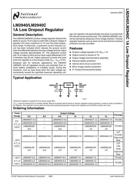
Typical Application<br />
January 2007<br />
The <strong>LM2940</strong>/<strong>LM2940</strong>C positive voltage regulator features the<br />
ability to source <strong>1A</strong> of output current with a dropout voltage of<br />
typically 0.5V and a maximum of 1V over the entire temperature<br />
range. Furthermore, a quiescent current reduction circuit<br />
has been included which reduces the ground current<br />
when the differential between the input voltage and the output<br />
voltage exceeds approximately 3V. The quiescent current<br />
with <strong>1A</strong> of output current and an input-output differential of 5V<br />
is therefore only 30 mA. Higher quiescent currents only exist<br />
when the regulator is in the dropout mode (V IN − V OUT ≤ 3V).<br />
Designed also for vehicular applications, the <strong>LM2940</strong>/<br />
<strong>LM2940</strong>C and all regulated circuitry are protected from reverse<br />
battery installations or 2-battery jumps. During line<br />
transients, such as load dump when the input voltage can<br />
momentarily exceed the specified maximum operating voltage,<br />
the regulator will automatically shut down to protect both<br />
the internal circuits and the load. The <strong>LM2940</strong>/<strong>LM2940</strong>C cannot<br />
be harmed by temporary mirror-image insertion. Familiar<br />
regulator features such as short circuit and thermal overload<br />
protection are also provided.<br />
Features<br />
■ <strong>Dropout</strong> voltage typically 0.5V @I O = <strong>1A</strong><br />
■ Output current in excess of <strong>1A</strong><br />
■ Output voltage trimmed before assembly<br />
■ Reverse battery protection<br />
■ Internal short circuit current limit<br />
■ Mirror image insertion protection<br />
■ P + Product Enhancement tested<br />
<strong>LM2940</strong>/<strong>LM2940</strong>C <strong>1A</strong> <strong>Low</strong> <strong>Dropout</strong> <strong>Regulator</strong><br />
*Required if regulator is located far from power supply filter.<br />
**C OUT must be at least 22 μF to maintain stability. May be increased without bound to maintain regulation during transients. Locate as close as possible to<br />
the regulator. This capacitor must be rated over the same operating temperature range as the regulator and the ESR is critical; see curve.<br />
Ordering Information<br />
882203<br />
Temp<br />
Range<br />
0°C<br />
≤ T J ≤<br />
125°C<br />
−40°C<br />
≤ T J ≤<br />
125°C<br />
−40°C<br />
≤ T J ≤<br />
125°C<br />
Output Voltage<br />
5.0 8.0 9.0 10 12 15<br />
Package<br />
<strong>LM2940</strong>CT-5.0 – <strong>LM2940</strong>CT-9.0 – <strong>LM2940</strong>CT-12 <strong>LM2940</strong>CT-15 TO-220<br />
<strong>LM2940</strong>CS-5.0 – <strong>LM2940</strong>CS-9.0 – <strong>LM2940</strong>CS-12 <strong>LM2940</strong>CS-15<br />
<strong>LM2940</strong>CSX<br />
-5.0<br />
–<br />
<strong>LM2940</strong>CSX<br />
-9.0<br />
–<br />
<strong>LM2940</strong>CSX<br />
-12<br />
<strong>LM2940</strong>CSX<br />
-15<br />
<strong>LM2940</strong>LD-5.0 <strong>LM2940</strong>LD-8.0 <strong>LM2940</strong>LD-9.0 <strong>LM2940</strong>LD-10 <strong>LM2940</strong>LD-12 <strong>LM2940</strong>LD-15<br />
<strong>LM2940</strong>LDX<br />
-5.0<br />
<strong>LM2940</strong>LDX<br />
-8.0<br />
<strong>LM2940</strong>LDX<br />
-9.0<br />
<strong>LM2940</strong>LDX<br />
-10<br />
<strong>LM2940</strong>LDX<br />
-12<br />
<strong>LM2940</strong>LDX<br />
-15<br />
TO-263<br />
LLP<br />
1k Units<br />
Tape and<br />
Reel<br />
LLP<br />
4.5k<br />
Units<br />
Tape and<br />
Reel<br />
<strong>LM2940</strong>T-5.0 <strong>LM2940</strong>T-8.0 <strong>LM2940</strong>T-9.0 <strong>LM2940</strong>T-10 <strong>LM2940</strong>T-12 – TO-220<br />
<strong>LM2940</strong>S-5.0 <strong>LM2940</strong>S-8.0 <strong>LM2940</strong>S-9.0 <strong>LM2940</strong>S-10 <strong>LM2940</strong>S-12 –<br />
<strong>LM2940</strong>SX-5.0 <strong>LM2940</strong>SX-8.0 <strong>LM2940</strong>SX-9.0 <strong>LM2940</strong>SX-10 <strong>LM2940</strong>SX-12 –<br />
TO-263<br />
© 2007 National Semiconductor Corporation 8822 www.national.com
<strong>LM2940</strong>/<strong>LM2940</strong>C<br />
Temp<br />
Range<br />
−40°C<br />
≤ T A ≤<br />
85°C<br />
Output Voltage<br />
5.0 8.0 9.0 10 12 15<br />
Package<br />
<strong>LM2940</strong>IMP-5.0 <strong>LM2940</strong>IMP-8.0 <strong>LM2940</strong>IMP-9.0 <strong>LM2940</strong>IMP-10 <strong>LM2940</strong>IMP-12 <strong>LM2940</strong>IMP-15 SOT-223<br />
<strong>LM2940</strong>IMPX<br />
-5.0<br />
<strong>LM2940</strong>IMPX<br />
-8.0<br />
<strong>LM2940</strong>IMPX<br />
-9.0<br />
<strong>LM2940</strong>IMPX<br />
-10<br />
<strong>LM2940</strong>IMPX<br />
-12<br />
<strong>LM2940</strong>IMPX<br />
-15<br />
Marking L53B L54B L0EB L55B L56B L70B<br />
SOT-223<br />
in Tape<br />
and Reel<br />
The physical size of the SOT-223 is too small to contain the full device part number. The package markings indicated are what will appear on the actual device.<br />
Mil-Aero Ordering Information<br />
Temperature<br />
Range<br />
−55°C<br />
≤ T J ≤<br />
125°C<br />
Output Voltage<br />
5.0 8.0 12 15<br />
<strong>LM2940</strong>J-5.0/883<br />
5962-8958701EA<br />
<strong>LM2940</strong>WG5.0/883<br />
5962-8958701XA<br />
–<br />
<strong>LM2940</strong>J-12/883<br />
5962-9088401QEA<br />
<strong>LM2940</strong>J-15/883<br />
5962-9088501QEA<br />
Package<br />
J16A<br />
– <strong>LM2940</strong>WG5-12/883 <strong>LM2940</strong>WG5-15/883 WG16A<br />
For information on military temperature range products, please go to the Mil/Aero Web Site at http://www.national.com/appinfo/milaero/index.html.<br />
Connection Diagrams<br />
TO-220 (T) Plastic Package<br />
SOT-223 (MP) 3-Lead<br />
882202<br />
Front View<br />
See NS Package Number TO3B<br />
16-Lead Dual-in-Line Package (J)<br />
882242<br />
Front View<br />
See NS Package Number MP04A<br />
16-Lead Ceramic Surface-Mount Package (WG)<br />
882243<br />
Top View<br />
See NS Package Number J16A<br />
882244<br />
Top View<br />
See NS Package Number WG16A<br />
TO-263 (S) Surface-Mount Package<br />
LLP (LD) 8-Lead<br />
Top View<br />
882211<br />
882212<br />
Side View<br />
See NS Package Number TS3B<br />
Pin 2 and pin 7 are fused to center DAP<br />
882246<br />
Pin 5 and 6 need to be tied together on PCB board<br />
Top View<br />
See NS Package Number LDC08A<br />
www.national.com 2
Absolute Maximum Ratings (Note 1)<br />
If Military/Aerospace specified devices are required,<br />
please contact the National Semiconductor Sales Office/<br />
Distributors for availability and specifications.<br />
<strong>LM2940</strong>S, J, WG, T, MP ≤ 100<br />
ms<br />
<strong>LM2940</strong>CS, T ≤ 1 ms<br />
Internal Power Dissipation<br />
60V<br />
45V<br />
(Note 2)<br />
Internally Limited<br />
Maximum Junction Temperature 150°C<br />
Storage Temperature Range<br />
Soldering Temperature (Note 3)<br />
TO-220 (T), Wave<br />
TO-263 (S)<br />
−65°C ≤ T J ≤ +150°C<br />
260°C, 10s<br />
235°C, 30s<br />
SOT-223 (MP)<br />
LLP-8 (LD)<br />
ESD Susceptibility (Note 4)<br />
Operating Conditions (Note 1)<br />
Input Voltage<br />
Temperature Range<br />
260°C, 30s<br />
235°C, 30s<br />
2 kV<br />
26V<br />
<strong>LM2940</strong>T, <strong>LM2940</strong>S −40°C ≤ T J ≤ 125°C<br />
<strong>LM2940</strong>CT, <strong>LM2940</strong>CS 0°C ≤ T J ≤ 125°C<br />
<strong>LM2940</strong>IMP −40°C ≤ T A ≤ 85°C<br />
<strong>LM2940</strong>J, <strong>LM2940</strong>WG −55°C ≤ T J ≤ 125°C<br />
<strong>LM2940</strong>LD −40°C ≤ T J ≤ 125°C<br />
Electrical Characteristics<br />
V IN = V O + 5V, I O = <strong>1A</strong>, C O = 22 μF, unless otherwise specified. Boldface limits apply over the entire operating temperature<br />
range of the indicated device. All other specifications apply for T A = T J = 25°C.<br />
Output Voltage (V O ) 5V 8V<br />
<strong>LM2940</strong> <strong>LM2940</strong>/883 <strong>LM2940</strong> <strong>LM2940</strong>/883<br />
Parameter Conditions Typ Limit Limit Typ Limit Limit<br />
(Note 5) (Note 6) (Note 5) (Note 6)<br />
6.25V ≤ V IN ≤ 26V 9.4V ≤ V IN ≤ 26V<br />
Units<br />
<strong>LM2940</strong>/<strong>LM2940</strong>C<br />
Output Voltage 5 mA ≤ I O ≤ <strong>1A</strong> 5.00 4.85/4.75 4.85/4.75 8.00 7.76/7.60 7.76/7.60 V MIN<br />
5.15/5.25 5.15/5.25 8.24/8.40 8.24/8.40 V MAX<br />
Line Regulation V O + 2V ≤ V IN ≤ 26V, 20 50 40/50 20 80 50/80 mV MAX<br />
I O = 5 mA<br />
Load Regulation 50 mA ≤ I O ≤ <strong>1A</strong><br />
Output 100 mADC and<br />
<strong>LM2940</strong>, <strong>LM2940</strong>/883 35 50/80 50/100 55 80/130 80/130 mV MAX<br />
<strong>LM2940</strong>C 35 50 55 80<br />
Impedance 20 mArms, 35 1000/1000 55 1000/1000 mΩ<br />
f O = 120 Hz<br />
Quiescent V O +2V ≤ V IN ≤ 26V,<br />
Current I O = 5 mA<br />
<strong>LM2940</strong>, <strong>LM2940</strong>/883 10 15/20 15/20 10 15/20 15/20 mA MAX<br />
<strong>LM2940</strong>C 10 15<br />
V IN = V O + 5V, 30 45/60 50/60 30 45/60 50/60 mA MAX<br />
I O = <strong>1A</strong><br />
Output Noise 10 Hz − 100 kHz, 150 700/700 240 1000/1000 μV rms<br />
Voltage I O = 5 mA<br />
Ripple Rejection f O = 120 Hz, 1 V rms ,<br />
I O = 100 mA<br />
<strong>LM2940</strong> 72 60/54 66 54/48 dB MIN<br />
<strong>LM2940</strong>C 72 60 66 54<br />
f O = 1 kHz, 1 V rms , 60/50 54/48 dB MIN<br />
I O = 5 mA<br />
Long Term 20 32 mV/<br />
Stability 1000 Hr<br />
<strong>Dropout</strong> Voltage I O = <strong>1A</strong> 0.5 0.8/1.0 0.7/1.0 0.5 0.8/1.0 0.7/1.0 V MAX<br />
I O = 100 mA 110 150/200 150/200 110 150/200 150/200 mV MAX<br />
3 www.national.com
<strong>LM2940</strong>/<strong>LM2940</strong>C<br />
Output Voltage (V O ) 5V 8V<br />
<strong>LM2940</strong> <strong>LM2940</strong>/883 <strong>LM2940</strong> <strong>LM2940</strong>/883<br />
Parameter Conditions Typ Limit Limit Typ Limit Limit<br />
Short Circuit<br />
Current<br />
(Note 7)<br />
Maximum Line R O = 100Ω<br />
(Note 5) (Note 6) (Note 5) (Note 6)<br />
Units<br />
1.9 1.6 1.5/1.3 1.9 1.6 1.6/1.3 A MIN<br />
Transient <strong>LM2940</strong>, T ≤ 100 ms 75 60/60 75 60/60<br />
Reverse Polarity R O = 100Ω<br />
<strong>LM2940</strong>/883, T ≤ 20 ms 40/40 40/40<br />
<strong>LM2940</strong>C, T ≤ 1 ms 55 45 55 45<br />
V MIN<br />
DC Input Voltage <strong>LM2940</strong>, <strong>LM2940</strong>/883 −30 −15/−15 −15/−15 −30 −15/−15 −15/−15 V MIN<br />
<strong>LM2940</strong>C −30 −15 −30 −15<br />
Reverse Polarity R O = 100Ω<br />
Transient Input <strong>LM2940</strong>, T ≤ 100 ms −75 −50/−50 −75 −50/−50 V MIN<br />
Voltage <strong>LM2940</strong>/883, T ≤ 20 ms −45/−45 −45/−45<br />
<strong>LM2940</strong>C, T ≤ 1 ms −55 −45/−45<br />
Electrical Characteristics<br />
V IN = V O + 5V, I O = <strong>1A</strong>, C O = 22 μF, unless otherwise specified. Boldface limits apply over the entire operating temperature<br />
range of the indicated device. All other specifications apply for T A = T J = 25°C.<br />
Output Voltage (V O ) 9V 10V<br />
Parameter Conditions Typ<br />
<strong>LM2940</strong><br />
Limit<br />
Typ<br />
<strong>LM2940</strong><br />
Limit<br />
(Note 5) (Note 5)<br />
10.5V ≤ V IN ≤ 26V 11.5V ≤ V IN ≤ 26V<br />
Output Voltage 5 mA ≤ I O ≤<strong>1A</strong> 9.00 8.73/8.55 10.00 9.70/9.50 V MIN<br />
Units<br />
9.27/9.45 10.30/10.50 V MAX<br />
Line Regulation V O + 2V ≤ V IN ≤ 26V, 20 90 20 100 mV MAX<br />
I O = 5 mA<br />
Load Regulation 50 mA ≤ I O ≤ <strong>1A</strong><br />
Output Impedance 100 mADC and<br />
<strong>LM2940</strong> 60 90/150 65 100/165 mV MAX<br />
<strong>LM2940</strong>C 60 90<br />
20 mArms, 60 65 mΩ<br />
f O = 120 Hz<br />
Quiescent V O +2V ≤ V IN < 26V,<br />
Current I O = 5 mA<br />
<strong>LM2940</strong> 10 15/20 10 15/20 mA MAX<br />
<strong>LM2940</strong>C 10 15<br />
V IN = V O + 5V, I O = <strong>1A</strong> 30 45/60 30 45/60 mA MAX<br />
Output Noise 10 Hz − 100 kHz, 270 300 μV rms<br />
Voltage I O = 5 mA<br />
Ripple Rejection f O = 120 Hz, 1 V rms ,<br />
I O = 100 mA<br />
Long Term<br />
Stability<br />
<strong>LM2940</strong> 64 52/46 63 51/45 dB MIN<br />
<strong>LM2940</strong>C 64 52<br />
34 36 mV/<br />
1000 Hr<br />
www.national.com 4
Output Voltage (V O ) 9V 10V<br />
<strong>LM2940</strong><br />
<strong>LM2940</strong><br />
Parameter Conditions Typ Limit Typ<br />
Limit<br />
Units<br />
(Note 5) (Note 5)<br />
<strong>Dropout</strong> Voltage I O = <strong>1A</strong> 0.5 0.8/1.0 0.5 0.8/1.0 V MAX<br />
I O = 100 mA 110 150/200 110 150/200 mV MAX<br />
<strong>LM2940</strong>/<strong>LM2940</strong>C<br />
Short Circuit (Note 7) 1.9 1.6 1.9 1.6 A MIN<br />
Current<br />
Maximum Line R O = 100Ω<br />
Transient T ≤ 100 ms<br />
Reverse Polarity R O = 100Ω<br />
<strong>LM2940</strong> 75 60/60 75 60/60 V MIN<br />
<strong>LM2940</strong>C 55 45<br />
DC Input Voltage <strong>LM2940</strong> −30 −15/−15 −30 −15/−15 V MIN<br />
<strong>LM2940</strong>C −30 −15<br />
Reverse Polarity R O = 100Ω<br />
Transient Input T ≤ 100 ms<br />
Voltage <strong>LM2940</strong> −75 −50/−50 −75 −50/−50 V MIN<br />
<strong>LM2940</strong>C −55 −45/−45<br />
Electrical Characteristics<br />
V IN = V O + 5V, I O = <strong>1A</strong>, C O = 22 μF, unless otherwise specified. Boldface limits apply over the entire operating temperature<br />
range of the indicated device. All other specifications apply for T A = T J = 25°C.<br />
Output Voltage (V O ) 12V 15V<br />
<strong>LM2940</strong> <strong>LM2940</strong>/833 <strong>LM2940</strong> <strong>LM2940</strong>/833<br />
Parameter Conditions Typ Limit Limit Typ Limit Limit<br />
(Note 5) (Note 6) (Note 5) (Note 6)<br />
13.6V ≤ V IN ≤ 26V 16.75V ≤ V IN ≤ 26V<br />
Output Voltage 5 mA ≤ I O ≤<strong>1A</strong> 12.00 11.64/11.40 11.64/11.40 15.00 14.55/14.25 14.55/14.25 V MIN<br />
Units<br />
12.36/12.60 12.36/12.60 15.45/15.75 15.45/15.75 V MAX<br />
Line Regulation V O + 2V ≤ V IN ≤ 26V, 20 120 75/120 20 150 95/150 mV MAX<br />
I O = 5 mA<br />
Load Regulation 50 mA ≤ I O ≤ <strong>1A</strong><br />
Output 100 mADC and<br />
<strong>LM2940</strong>, <strong>LM2940</strong>/883 55 120/200 120/190 150/240 mV MAX<br />
<strong>LM2940</strong>C 55 120 70 150<br />
Impedance 20 mArms, 80 1000/1000 100 1000/1000 mΩ<br />
Quiescent<br />
Current<br />
f O = 120 Hz<br />
V O +2V ≤ V IN ≤ 26V,<br />
I O = 5 mA<br />
<strong>LM2940</strong>, <strong>LM2940</strong>/883 10 15/20 15/20 15/20 mA MAX<br />
<strong>LM2940</strong>C 10 15 10 15<br />
V IN = V O + 5V, I O = <strong>1A</strong> 30 45/60 50/60 30 45/60 50/60 mA MAX<br />
Output Noise 10 Hz − 100 kHz, 360 1000/1000 450 1000/1000 μV rms<br />
Voltage I O = 5 mA<br />
5 www.national.com
<strong>LM2940</strong>/<strong>LM2940</strong>C<br />
Output Voltage (V O ) 12V 15V<br />
<strong>LM2940</strong> <strong>LM2940</strong>/833 <strong>LM2940</strong> <strong>LM2940</strong>/833<br />
Parameter Conditions Typ Limit Limit Typ Limit Limit<br />
Ripple Rejection f O = 120 Hz, 1 V rms ,<br />
I O = 100 mA<br />
(Note 5) (Note 6) (Note 5) (Note 6)<br />
Units<br />
<strong>LM2940</strong> 66 54/48 dB MIN<br />
<strong>LM2940</strong>C 66 54 64 52<br />
f O = 1 kHz, 1 V rms ,<br />
I O = 5 mA<br />
52/46 48/42<br />
Long Term<br />
mV/<br />
48 60<br />
Stability 1000 Hr<br />
<strong>Dropout</strong> Voltage I O = <strong>1A</strong> 0.5 0.8/1.0 0.7/1.0 0.5 0.8/1.0 0.7/1.0 V MAX<br />
Short Circuit (Note 7)<br />
Current<br />
Maximum Line R O = 100Ω<br />
dB MIN<br />
I O = 100 mA 110 150/200 150/200 110 150/200 150/200 mV MAX<br />
Transient <strong>LM2940</strong>, T ≤ 100 ms 75 60/60<br />
Reverse Polarity R O = 100Ω<br />
1.9 1.6 1.6/1.3 1.9 1.6 1.6/1.3 A MIN<br />
<strong>LM2940</strong>/883, T ≤ 20 ms 40/40 40/40 V MIN<br />
<strong>LM2940</strong>C, T ≤ 1 ms 55 45 55 45<br />
DC Input <strong>LM2940</strong>, <strong>LM2940</strong>/883 −30 −15/−15 −15/−15 −15/−15 V MIN<br />
Voltage <strong>LM2940</strong>C −30 −15 −30 −15<br />
Reverse Polarity R O = 100Ω<br />
Transient Input <strong>LM2940</strong>, T ≤ 100 ms −75 −50/−50<br />
Voltage <strong>LM2940</strong>/883, T ≤ 20 ms −45/−45 −45/−45 V MIN<br />
Thermal Performance<br />
<strong>LM2940</strong>C, T ≤ 1 ms −55 −45/−45 −55 −45/−45<br />
Thermal Resistance<br />
Junction-to-Case, θ (JC)<br />
3-Lead TO-220<br />
3-Lead TO-263<br />
4<br />
4<br />
Junction-to-Ambient, θ (JA) SOT-223(Note 2) 174<br />
3-Lead TO-220 (Note 2) 60<br />
Thermal Resistance<br />
3-Lead TO-263 (Note 2) 80<br />
8-Lead LLP (Note 2) 35<br />
°C/W<br />
°C/W<br />
Note 1: Absolute Maximum Ratings are limits beyond which damage to the device may occur. Operating Conditions are conditions under which the device<br />
functions but the specifications might not be guaranteed. For guaranteed specifications and test conditions see the Electrical Characteristics.<br />
Note 2: The maximum allowable power dissipation is a function of the maximum junction temperature, T J , the junction-to-ambient thermal resistance, θ JA , and<br />
the ambient temperature, T A . Exceeding the maximum allowable power dissipation will cause excessive die temperature, and the regulator will go into thermal<br />
shutdown. The value of θ JA (for devices in still air with no heatsink) is 60°C/W for the TO-220 package, 80°C/W for the TO-263 package, and 174°C/W for the<br />
SOT-223 package. The effective value of θ JA can be reduced by using a heatsink (see Application Hints for specific information on heatsinking). The value of<br />
θ JA for the LLP package is specifically dependent on PCB trace area, trace material, and the number of layers and thermal vias. For improved thermal resistance<br />
and power dissipation for the LLP package, refer to Application Note AN-1187. It is recommended that 6 vias be placed under the center pad to improve thermal<br />
performance.<br />
Note 3: Refer to JEDEC J-STD-020C for surface mount device (SMD) package reflow profiles and conditions. Unless otherwise stated, the temperature and time<br />
are for Sn-Pb (STD) only.<br />
Note 4: ESD rating is based on the human body model, 100 pF discharged through 1.5 kΩ.<br />
Note 5: All limits are guaranteed at T A = T J = 25°C only (standard typeface) or over the entire operating temperature range of the indicated device (boldface type).<br />
All limits at T A = T J = 25°C are 100% production tested. All limits at temperature extremes are guaranteed via correlation using standard Statistical Quality Control<br />
methods.<br />
Note 6: All limits are guaranteed at T A = T J = 25°C only (standard typeface) or over the entire operating temperature range of the indicated device (boldface type).<br />
All limits are 100% production tested and are used to calculate Outgoing Quality Levels.<br />
Note 7: Output current will decrease with increasing temperature but will not drop below <strong>1A</strong> at the maximum specified temperature.<br />
www.national.com 6
Typical Performance Characteristics<br />
<strong>Dropout</strong> Voltage<br />
<strong>Dropout</strong> Voltage vs. Temperature<br />
<strong>LM2940</strong>/<strong>LM2940</strong>C<br />
882213<br />
882214<br />
Output Voltage vs. Temperature<br />
Quiescent Current vs. Temperature<br />
882215<br />
882216<br />
Quiescent Current<br />
Quiescent Current<br />
882217<br />
882218<br />
7 www.national.com
<strong>LM2940</strong>/<strong>LM2940</strong>C<br />
Line Transient Response<br />
Load Transient Response<br />
882219<br />
882220<br />
Ripple Rejection<br />
<strong>Low</strong> Voltage Behavior<br />
882221<br />
882225<br />
<strong>Low</strong> Voltage Behavior<br />
<strong>Low</strong> Voltage Behavior<br />
882226<br />
882227<br />
www.national.com 8
<strong>Low</strong> Voltage Behavior<br />
<strong>Low</strong> Voltage Behavior<br />
<strong>LM2940</strong>/<strong>LM2940</strong>C<br />
882228<br />
882229<br />
<strong>Low</strong> Voltage Behavior<br />
Output at Voltage Extremes<br />
882230<br />
882231<br />
Output at Voltage Extremes<br />
Output at Voltage Extremes<br />
882232<br />
882233<br />
9 www.national.com
<strong>LM2940</strong>/<strong>LM2940</strong>C<br />
Output at Voltage Extremes<br />
Output at Voltage Extremes<br />
882234<br />
882235<br />
Output at Voltage Extremes<br />
Output Capacitor ESR<br />
882236<br />
882206<br />
Peak Output Current<br />
Output Impedance<br />
882208<br />
882222<br />
www.national.com 10
Maximum Power Dissipation (TO-220)<br />
Maximum Power Dissipation (SOT-223)<br />
<strong>LM2940</strong>/<strong>LM2940</strong>C<br />
882223<br />
882224<br />
Maximum Power Dissipation (TO-263)<br />
882210<br />
11 www.national.com
<strong>LM2940</strong>/<strong>LM2940</strong>C<br />
Equivalent Schematic Diagram<br />
882201<br />
www.national.com 12
Application Information<br />
EXTERNAL CAPACITORS<br />
The output capacitor is critical to maintaining regulator stability,<br />
and must meet the required conditions for both ESR<br />
(Equivalent Series Resistance) and minimum amount of capacitance.<br />
MINIMUM CAPACITANCE:<br />
The minimum output capacitance required to maintain stability<br />
is 22 μF (this value may be increased without limit). Larger<br />
values of output capacitance will give improved transient response.<br />
ESR LIMITS:<br />
The ESR of the output capacitor will cause loop instability if it<br />
is too high or too low. The acceptable range of ESR plotted<br />
versus load current is shown in the graph below. It is essential<br />
that the output capacitor meet these requirements, or<br />
oscillations can result.<br />
Output Capacitor ESR<br />
temperature must be within the range specified under Absolute<br />
Maximum Ratings.<br />
To determine if a heatsink is required, the power dissipated<br />
by the regulator, P D , must be calculated.<br />
The figure below shows the voltages and currents which are<br />
present in the circuit, as well as the formula for calculating the<br />
power dissipated in the regulator:<br />
I IN = I L + I G<br />
P D = (V IN − V OUT ) I L + (V IN ) I G<br />
FIGURE 2. Power Dissipation Diagram<br />
882237<br />
The next parameter which must be calculated is the maximum<br />
allowable temperature rise, T R(MAX) . This is calculated by using<br />
the formula:<br />
<strong>LM2940</strong>/<strong>LM2940</strong>C<br />
T R(MAX) = T J(MAX) − T A(MAX)<br />
FIGURE 1. ESR Limits<br />
882206<br />
It is important to note that for most capacitors, ESR is specified<br />
only at room temperature. However, the designer must<br />
ensure that the ESR will stay inside the limits shown over the<br />
entire operating temperature range for the design.<br />
For aluminum electrolytic capacitors, ESR will increase by<br />
about 30X as the temperature is reduced from 25°C to −40°<br />
C. This type of capacitor is not well-suited for low temperature<br />
operation.<br />
Solid tantalum capacitors have a more stable ESR over temperature,<br />
but are more expensive than aluminum electrolytics.<br />
A cost-effective approach sometimes used is to parallel<br />
an aluminum electrolytic with a solid Tantalum, with the total<br />
capacitance split about 75/25% with the Aluminum being the<br />
larger value.<br />
If two capacitors are paralleled, the effective ESR is the parallel<br />
of the two individual values. The “flatter” ESR of the<br />
Tantalum will keep the effective ESR from rising as quickly at<br />
low temperatures.<br />
where: T J(MAX)<br />
T A(MAX)<br />
is the maximum allowable junction temperature,<br />
which is 125°C for commercial grade<br />
parts.<br />
is the maximum ambient temperature which<br />
will be encountered in the application.<br />
Using the calculated values for T R(MAX) and P D , the maximum<br />
allowable value for the junction-to-ambient thermal resistance,<br />
θ (JA) , can now be found:<br />
θ (JA) = T R(MAX) / P D<br />
IMPORTANT: If the maximum allowable value for θ (JA) is<br />
found to be ≥ 53°C/W for the TO-220 package, ≥ 80°C/W for<br />
the TO-263 package, or ≥ 174°C/W for the SOT-223 package,<br />
no heatsink is needed since the package alone will<br />
dissipate enough heat to satisfy these requirements.<br />
If the calculated value for θ (JA) falls below these limits, a<br />
heatsink is required.<br />
HEATSINKING TO-220 PACKAGE PARTS<br />
The TO-220 can be attached to a typical heatsink, or secured<br />
to a copper plane on a PC board. If a copper plane is to be<br />
used, the values of θ (JA) will be the same as shown in the next<br />
section for the TO-263.<br />
If a manufactured heatsink is to be selected, the value of<br />
heatsink-to-ambient thermal resistance, θ (H−A) , must first be<br />
calculated:<br />
θ (H−A) = θ (JA) − θ (C−H) − θ (J−C)<br />
HEATSINKING<br />
A heatsink may be required depending on the maximum power<br />
dissipation and maximum ambient temperature of the application.<br />
Under all possible operating conditions, the junction<br />
Where: θ (J−C)<br />
is defined as the thermal resistance from the<br />
junction to the surface of the case. A value of<br />
3°C/W can be assumed for θ (J−C) for this calculation.<br />
13 www.national.com
<strong>LM2940</strong>/<strong>LM2940</strong>C<br />
θ (C−H)<br />
is defined as the thermal resistance between<br />
the case and the surface of the heatsink. The<br />
value of θ (C−H) will vary from about 1.5°C/W to<br />
about 2.5°C/W (depending on method of attachment,<br />
insulator, etc.). If the exact value is<br />
unknown, 2°C/W should be assumed for θ (C<br />
−H) .<br />
When a value for θ (H−A) is found using the equation shown, a<br />
heatsink must be selected that has a value that is less than<br />
or equal to this number.<br />
θ (H−A) is specified numerically by the heatsink manufacturer<br />
in the catalog, or shown in a curve that plots temperature rise<br />
vs power dissipation for the heatsink.<br />
HEATSINKING TO-263 PACKAGE PARTS<br />
The TO-263 (“S”) package uses a copper plane on the PCB<br />
and the PCB itself as a heatsink. To optimize the heat sinking<br />
ability of the plane and PCB, solder the tab of the package to<br />
the plane.<br />
Figure 3 shows for the TO-263 the measured values of θ (JA)<br />
for different copper area sizes using a typical PCB with 1<br />
ounce copper and no solder mask over the copper area used<br />
for heatsinking.<br />
882239<br />
FIGURE 4. Maximum Power Dissipation vs. T A for the<br />
TO-263 Package<br />
HEATSINKING SOT-223 PACKAGE PARTS<br />
The SOT-223 (“MP”) packages use a copper plane on the<br />
PCB and the PCB itself as a heatsink. To optimize the heat<br />
sinking ability of the plane and PCB, solder the tab of the<br />
package to the plane.<br />
Figure 5 and Figure 6 show the information for the SOT-223<br />
package. Figure 6 assumes a θ (JA) of 74°C/W for 1 square<br />
inch of 1 ounce copper and 51°C/W for 1 square inch of 2<br />
ounce copper, with a maximum ambient temperature (T A ) of<br />
85°C and a maximum junction temperature (T J ) of 125°C.<br />
For techniques for improving the thermal resistance and power<br />
dissipation for the SOT-223 package, please refer to Application<br />
Note AN-1028.<br />
882238<br />
FIGURE 3. θ (JA) vs. Copper (1 ounce) Area for the TO-263<br />
Package<br />
As shown in the figure, increasing the copper area beyond 1<br />
square inch produces very little improvement. It should also<br />
be observed that the minimum value of θ (JA) for the TO-263<br />
package mounted to a PCB is 32°C/W.<br />
As a design aid, Figure 4 shows the maximum allowable power<br />
dissipation compared to ambient temperature for the<br />
TO-263 device. This assumes a θ (JA) of 35°C/W for 1 square<br />
inch of 1 ounce copper and a maximum junction temperature<br />
(T J ) of 125°C.<br />
882240<br />
FIGURE 5. θ (JA) vs. Copper (2 ounce) Area for the SOT-223<br />
Package<br />
www.national.com 14
HEATSINKING LLP PACKAGE PARTS<br />
The value of θ JA for the LLP package is specifically dependent<br />
on PCB trace area, trace material, and the number of layers<br />
and thermal vias. It is recommended that a minimum of 6<br />
thermal vias be placed under the center pad to improve thermal<br />
performance.<br />
For techniques for improving the thermal resistance and power<br />
dissipation for the LLP package, please refer to Application<br />
Note AN-1187.<br />
<strong>LM2940</strong>/<strong>LM2940</strong>C<br />
882241<br />
FIGURE 6. Maximum Power Dissipation vs. T A for the<br />
SOT-223 Package<br />
15 www.national.com
<strong>LM2940</strong>/<strong>LM2940</strong>C<br />
Physical Dimensions inches (millimeters) unless otherwise noted<br />
3-Lead SOT-223 Package<br />
NS Package Number MP04A<br />
16 Lead Dual-in-Line Package (J)<br />
See NS Package Number J16A<br />
www.national.com 16
<strong>LM2940</strong>/<strong>LM2940</strong>C<br />
16 Lead Surface Mount Package (WG)<br />
See NS Package Number WG16A<br />
3-Lead TO-220 Plastic Package (T)<br />
NS Package Number TO3B<br />
17 www.national.com
<strong>LM2940</strong>/<strong>LM2940</strong>C<br />
3-Lead TO-263 Surface Mount Package (MP)<br />
NS Package Number TS3B<br />
8-Lead LLP<br />
Order Number <strong>LM2940</strong>LD-5.0, <strong>LM2940</strong>LD-8.0,<br />
<strong>LM2940</strong>LD-9.0, <strong>LM2940</strong>LD-10,<br />
<strong>LM2940</strong>LD-12 or <strong>LM2940</strong>LD-15<br />
NS Package Number LDC08A<br />
www.national.com 18
Notes<br />
<strong>LM2940</strong>/<strong>LM2940</strong>C<br />
19 www.national.com
<strong>LM2940</strong>/<strong>LM2940</strong>C <strong>1A</strong> <strong>Low</strong> <strong>Dropout</strong> <strong>Regulator</strong><br />
Notes<br />
THE CONTENTS OF THIS DOCUMENT ARE PROVIDED IN CONNECTION WITH NATIONAL SEMICONDUCTOR CORPORATION<br />
(“NATIONAL”) PRODUCTS. NATIONAL MAKES NO REPRESENTATIONS OR WARRANTIES WITH RESPECT TO THE ACCURACY<br />
OR COMPLETENESS OF THE CONTENTS OF THIS PUBLICATION AND RESERVES THE RIGHT TO MAKE CHANGES TO<br />
SPECIFICATIONS AND PRODUCT DESCRIPTIONS AT ANY TIME WITHOUT NOTICE. NO LICENSE, WHETHER EXPRESS,<br />
IMPLIED, ARISING BY ESTOPPEL OR OTHERWISE, TO ANY INTELLECTUAL PROPERTY RIGHTS IS GRANTED BY THIS<br />
DOCUMENT.<br />
TESTING AND OTHER QUALITY CONTROLS ARE USED TO THE EXTENT NATIONAL DEEMS NECESSARY TO SUPPORT<br />
NATIONAL’S PRODUCT WARRANTY. EXCEPT WHERE MANDATED BY GOVERNMENT REQUIREMENTS, TESTING OF ALL<br />
PARAMETERS OF EACH PRODUCT IS NOT NECESSARILY PERFORMED. NATIONAL ASSUMES NO LIABILITY FOR<br />
APPLICATIONS ASSISTANCE OR BUYER PRODUCT DESIGN. BUYERS ARE RESPONSIBLE FOR THEIR PRODUCTS AND<br />
APPLICATIONS USING NATIONAL COMPONENTS. PRIOR TO USING OR DISTRIBUTING ANY PRODUCTS THAT INCLUDE<br />
NATIONAL COMPONENTS, BUYERS SHOULD PROVIDE ADEQUATE DESIGN, TESTING AND OPERATING SAFEGUARDS.<br />
EXCEPT AS PROVIDED IN NATIONAL’S TERMS AND CONDITIONS OF SALE FOR SUCH PRODUCTS, NATIONAL ASSUMES NO<br />
LIABILITY WHATSOEVER, AND NATIONAL DISCLAIMS ANY EXPRESS OR IMPLIED WARRANTY RELATING TO THE SALE<br />
AND/OR USE OF NATIONAL PRODUCTS INCLUDING LIABILITY OR WARRANTIES RELATING TO FITNESS FOR A PARTICULAR<br />
PURPOSE, MERCHANTABILITY, OR INFRINGEMENT OF ANY PATENT, COPYRIGHT OR OTHER INTELLECTUAL PROPERTY<br />
RIGHT.<br />
LIFE SUPPORT POLICY<br />
NATIONAL’S PRODUCTS ARE NOT AUTHORIZED FOR USE AS CRITICAL COMPONENTS IN LIFE SUPPORT DEVICES OR<br />
SYSTEMS WITHOUT THE EXPRESS PRIOR WRITTEN APPROVAL OF THE CHIEF EXECUTIVE OFFICER AND GENERAL<br />
COUNSEL OF NATIONAL SEMICONDUCTOR CORPORATION. As used herein:<br />
Life support devices or systems are devices which (a) are intended for surgical implant into the body, or (b) support or sustain life and<br />
whose failure to perform when properly used in accordance with instructions for use provided in the labeling can be reasonably expected<br />
to result in a significant injury to the user. A critical component is any component in a life support device or system whose failure to perform<br />
can be reasonably expected to cause the failure of the life support device or system or to affect its safety or effectiveness.<br />
National Semiconductor and the National Semiconductor logo are registered trademarks of National Semiconductor Corporation. All other<br />
brand or product names may be trademarks or registered trademarks of their respective holders.<br />
Copyright© 2007 National Semiconductor Corporation<br />
For the most current product information visit us at www.national.com<br />
National Semiconductor<br />
Americas Customer<br />
Support Center<br />
Email:<br />
new.feedback@nsc.com<br />
Tel: 1-800-272-9959<br />
National Semiconductor Europe<br />
Customer Support Center<br />
Fax: +49 (0) 180-530-85-86<br />
Email: europe.support@nsc.com<br />
Deutsch Tel: +49 (0) 69 9508 6208<br />
English Tel: +49 (0) 870 24 0 2171<br />
Français Tel: +33 (0) 1 41 91 8790<br />
National Semiconductor Asia<br />
Pacific Customer Support Center<br />
Email: ap.support@nsc.com<br />
National Semiconductor Japan<br />
Customer Support Center<br />
Fax: 81-3-5639-7507<br />
Email: jpn.feedback@nsc.com<br />
Tel: 81-3-5639-7560<br />
www.national.com