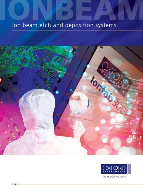
Ion beam etch and deposition systems
Ion beam etch and deposition systems
Ion beam etch and deposition systems

Create successful ePaper yourself
Turn your PDF publications into a flip-book with our unique Google optimized e-Paper software.
onbeaM<br />
<strong>Ion</strong> <strong>beam</strong> <strong>etch</strong> <strong>and</strong> <strong>deposition</strong> <strong>systems</strong>
<strong>Ion</strong> <strong>beam</strong> <strong>systems</strong><br />
ion<br />
<strong>Ion</strong> <strong>beam</strong> technology offers unique<br />
abilities in <strong>etch</strong> <strong>and</strong> <strong>deposition</strong><br />
Oxford Instruments offers a single tool, allowing the flexibility to<br />
perform <strong>etch</strong> <strong>and</strong>/or <strong>deposition</strong>, maximising system utilisation.<br />
System specifications can be closely tuned to applications, enabling<br />
faster <strong>and</strong> repeatable process results. The Oxford Instruments <strong>Ion</strong><br />
Beam range offers functionality in multiple modes:<br />
• <strong>Ion</strong> Beam Etching / Milling (IBE)<br />
• Reactive <strong>Ion</strong> Beam Etching (RIBE)<br />
•<br />
• <strong>Ion</strong> Beam Sputter Deposition (IBSD)<br />
• <strong>Ion</strong> Assisted Sputter Deposition (IASD)<br />
• Reactive <strong>Ion</strong> Beam Sputter Deposition (RIBD)<br />
Chemically Assisted <strong>Ion</strong> Beam Etching (CAIBE)<br />
Oxford Instruments’ <strong>systems</strong> are scalable from R&D to batch<br />
production in one tool.<br />
The <strong>Ion</strong> Beam Range<br />
<strong>Ion</strong>fab300Plus<br />
Optofab3000<br />
<strong>Ion</strong>fab500Plus<br />
Etch <strong>and</strong> <strong>deposition</strong> processes in one<br />
tool<br />
Purpose made system for optical<br />
coatings<br />
Specialist large-batch high precision<br />
ion <strong>beam</strong> <strong>deposition</strong> system<br />
Typical applications <strong>and</strong> materials<br />
• IR detectors<br />
• CdHgTe (CMT) <strong>etch</strong><br />
• VO <strong>deposition</strong> <strong>and</strong> <strong>etch</strong><br />
x<br />
• Metal contact <strong>and</strong> track <strong>etch</strong><br />
• Cu, Ni, Al…<br />
• Noble metals: Au, Pt, Pd…<br />
• Diffraction gratings<br />
• SiO ‘blazed’ <strong>etch</strong><br />
2<br />
• Spintronics <strong>and</strong> MRAM<br />
• AR <strong>and</strong> HR coatings for<br />
laser bars<br />
• Telecom filters<br />
• III-V photonics <strong>etch</strong>ing<br />
• Thin film magnetic hard<br />
drive heads (TFMH)<br />
•<br />
Ring laser gyroscope mirrors<br />
CCTV<br />
Fibre optic cable<br />
Thin film magnetic heads<br />
Night vision <strong>and</strong> security equipment<br />
<strong>Ion</strong> Beam
<strong>Ion</strong>fab<br />
<strong>beam</strong><br />
® 300Plus<br />
<strong>Ion</strong>fab300Plus is a modular System designed for ion <strong>beam</strong><br />
<strong>etch</strong>ing <strong>and</strong> <strong>deposition</strong>. It is used in a wide variety of processes,<br />
particularly in the Semiconductor <strong>and</strong> Optical Coating Industries<br />
Flexibility in a single tool<br />
•<br />
200 mm (8 inch) wafers<br />
• Wafer h<strong>and</strong>ling options<br />
H<strong>and</strong>les from small pieces, through 100 mm (4 inch), up to<br />
• Manual loading for one-off trials<br />
• Load-lock for faster trials, increased throughput <strong>and</strong><br />
improved particulate control<br />
• Cassette-to-cassette loading/unloading for batch production<br />
• Clusterable with other process tools including Oxford Instruments’<br />
Plasmalab ® plasma <strong>etch</strong>, <strong>deposition</strong> <strong>and</strong> sputtering tools, <strong>and</strong><br />
FlexAL ® atomic layer <strong>deposition</strong> (ALD) tools<br />
•<br />
Simple upgrade options to add an <strong>etch</strong> or <strong>deposition</strong> source<br />
Leading ion source <strong>and</strong> grid set<br />
technology<br />
•<br />
uniformity, high rate <strong>and</strong>/or low energy<br />
•<br />
Grids are designed to suit specific applications: high<br />
Specific <strong>deposition</strong> grid sets to suit multiple targets, offer<br />
superior utilisation of target material with minimisation of<br />
contamination<br />
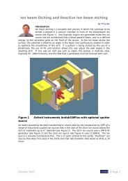
<strong>Ion</strong>fab300Plus tool<br />
images produced with the<br />
cooperation of the Optoelectronics Research<br />
Centre, University of Southampton, UK<br />
Easy to site, use <strong>and</strong> maintain<br />
•<br />
in “grey area”<br />
•<br />
•<br />
•<br />
Through-wall interface options allow the system to be sited<br />
Ease of access to process chamber via doors at either end<br />
Ease of maintenance with door-mounted ion sources<br />
Compact footprint reduces cleanroom space required<br />
<strong>Ion</strong><br />
PlasmalabSystem100<br />
FlexAL<br />
Beam
ion<br />
Specifically developed for high quality optical applications,<br />
Optofab ® 3000<br />
including High Reflective <strong>and</strong> Anti Reflective Coatings<br />
High speed<br />
specimen holder<br />
with uniformity<br />
shield<br />
Optofab3000 is based on the proven architecture of the<br />
<strong>Ion</strong>fab300Plus – offering the same features <strong>and</strong> benefits as<br />
the <strong>Ion</strong>fab300Plus but with added capabilities.<br />
•<br />
The high speed 8” specimen holder fitted to the system,<br />
delivers uniformity of < +/- 1%, <strong>and</strong> very good layer to<br />
layer repeatability. The option to use uniformity shields is<br />
available with this system, offering further improvements in<br />
layer uniformity.<br />
•<br />
A high <strong>deposition</strong> rate is achievable through the use of the<br />
15cm ion source, with a tailor made dished molybdenum<br />
3 grid design. In addition excellent refractive index control<br />
may be achieved with the use of an assist source.<br />
•<br />
The option to use a white light optical monitor is available<br />
with the Optofab3000 patented specimen holder. This<br />
is essential in ensuring that each layer is applied at the<br />
correct thickness, thereby achieving the specified optical<br />
characteristics of narrow b<strong>and</strong> filters, for example.<br />
In-situ monitoring of optical<br />
coating <strong>deposition</strong> by an<br />
integrated software package<br />
Simulation of a high<br />
performance optical filter by an<br />
integrated software package<br />
Multi-layer optical coating<br />
design by an integrated<br />
software package<br />
<strong>Ion</strong> Beam
eam<br />
Process <strong>and</strong> materials capability<br />
<strong>Ion</strong>fab300Plus <strong>and</strong> Optofab3000<br />
Etch <strong>and</strong> <strong>deposition</strong> in one tool via single or dual-<strong>beam</strong> technology<br />
• 15cm <strong>and</strong> 35cm source options available<br />
•<br />
Dual <strong>beam</strong> configurations (<strong>etch</strong> plus <strong>deposition</strong> source)<br />
offer the possibility to add capping layers immediately<br />
after <strong>etch</strong>, without exposing the process chamber or<br />
wafer to atmosphere<br />
• Increased <strong>deposition</strong> rates or improved material<br />
properties by using <strong>etch</strong> source as a plasma radical or<br />
assist source (IASD or RIBD)<br />
•<br />
•<br />
Deposit different material layers without breaking vacuum<br />
4”, 6” <strong>and</strong> 8” target sizes available<br />
A<br />
B<br />
Interior of the <strong>Ion</strong>fab300Plus<br />
C<br />
D<br />
Vacuum options to suit process<br />
• Turbo-pump fitted as st<strong>and</strong>ard<br />
•<br />
• Additional water vapour cryo trap option<br />
Cryo-pump option for moisture-sensitive applications<br />
A. CdHgTe (CMT) <strong>etch</strong> for<br />
infrared detector applications<br />
B. ‘Blazed’ quartz <strong>etch</strong> for<br />
diffraction grating<br />
C. LiNbO 3<br />
<strong>etch</strong><br />
D. RIBE of GaAs <strong>and</strong> AlGaAs.<br />
Courtesy of Chalmers<br />
University, Sweden<br />
<strong>Ion</strong> Beam
ion<br />
<strong>Ion</strong>fab300Plus <strong>and</strong> Optofab3000<br />
Process control<br />
Flexibility in a single tool<br />
•<br />
Tiltable substrate holder can be angled from<br />
-90° (load position) up to +65° (depending upon<br />
configuration)<br />
• Enables ‘blazed’ gratings<br />
• Allows sidewalls to be cleaned off or <strong>etch</strong>ed<br />
•<br />
•<br />
Allows excellent control of <strong>deposition</strong> uniformity<br />
Allows directional <strong>deposition</strong> for step coverage<br />
Platen rotation speed<br />
• St<strong>and</strong>ard <strong>and</strong> high speed platen options<br />
Process tool software<br />
The intuitive, user-friendly PC3000 TM graphical interface <strong>and</strong><br />
control software for the <strong>Ion</strong>fab300Plus offers:<br />
• Fast user learning<br />
• Full process recipe editing<br />
•<br />
endpointing<br />
•<br />
•<br />
Real-time visibility of process data including SIMS<br />
Automatic process <strong>and</strong> system data logging during runs<br />
Multi-level password-controlled user access for safe <strong>and</strong><br />
secure operation<br />
Substrate cooling<br />
•<br />
structures/other materials already in place<br />
• Option for wafer backside cooling with<br />
Prevents degradation of substrate <strong>and</strong> devices<br />
He (turbo-pump) or Ar (cryo-pump)<br />
Etch endpoint monitoring by SIMS for multi-<br />
Process monitoring<br />
•<br />
material applications<br />
•<br />
Deposition process monitoring<br />
• Crystal monitor (single or dual head)<br />
• White Light Optical Monitor (WLOM)<br />
•<br />
Chamber gas identification, partial pressure<br />
control <strong>and</strong> leak checking via RGA<br />
The PC3000<br />
graphical<br />
interface showing<br />
chamber <strong>and</strong><br />
load lock status<br />
Screen shot of system including<br />
cassette loading & robotic h<strong>and</strong>ling<br />
The process page provides complete control<br />
<strong>and</strong> visibility of the process being run<br />
<strong>Ion</strong> Beam
eam<br />
Specialist high-precision ion <strong>deposition</strong> system<br />
<strong>Ion</strong>fab ® 500Plus: Designed for ultra high quality optical thin films<br />
The <strong>Ion</strong>fab500Plus was first supplied in 1983 <strong>and</strong> was<br />
the world’s first commercial ion <strong>beam</strong> sputter <strong>deposition</strong><br />
system for ring laser gyroscope manufacture. In recent years<br />
customers have demonstrated mirrors exhibiting < 20ppm on<br />
a commercially available system using the <strong>Ion</strong>fab500Plus.<br />
The <strong>Ion</strong>fab500Plus has been developed for the requirements<br />
of customers dem<strong>and</strong>ing high throughput. This is delivered by<br />
the use of the 4 x 10” planetary substrates <strong>and</strong> the ability to<br />
use 14” targets.<br />
Another key benefit to customers requiring high throughput<br />
is the use of up to 3 targets, meaning that different material<br />
layers may be deposited without breaking vacuum.<br />
Low loss mirrors produced by <strong>Ion</strong> Beam<br />
sputter <strong>deposition</strong> are incorporated into this<br />
inertia sensor assembly which incorporates<br />
three ring laser gyroscopes. Image courtesy<br />
of Marconi Electric Systems<br />
Transmission spectrum of a mirror designed for 633 nm<br />
at 45°, deposited in the <strong>Ion</strong>fab500Plus, showing:<br />
• Mirror loss < 40 ppm<br />
• Uniformity < ±0.0005<br />
• Surface Roughness < 0.11 nm<br />
Excellent refractive index (RI) control <strong>and</strong> uniformity<br />
provides high product yield<br />
Designed<br />
for ultra high<br />
quality optical<br />
thin films!<br />
<strong>Ion</strong> Beam
n Plasma Etch & Deposition n Atomic Layer Deposition n <strong>Ion</strong> Beam Etch & Deposition n Nanoscale Growth Systems n HVPE<br />
onbeaM<br />
For further information about <strong>Ion</strong> Beam, please contact<br />
your local Oxford Instruments office<br />
Worldwide Service <strong>and</strong> Support<br />
Oxford Instruments is committed to supporting our customers’ success. We recognise that<br />
this requires world class products complemented by world class support. Our global service<br />
force is backed by regional offices, offering rapid support wherever you are in the world.<br />
We can provide:<br />
•<br />
•<br />
•<br />
•<br />
Tailored service agreements to meet your needs<br />
Comprehensive range of structured training courses<br />
Immediate access to genuine spare parts <strong>and</strong> accessories<br />
System upgrades <strong>and</strong> refurbishments<br />
Oxford Instruments<br />
Plasma Technology<br />
For more information please email:<br />
plasma@oxinst.com<br />
UK<br />
Yatton<br />
Tel: +44 (0)1934 837000<br />
Germany<br />
Wiesbaden<br />
Tel: +49 (0)6122 937 161<br />
Japan<br />
Tokyo<br />
Tel: +81 3 5245 3261<br />
PR China<br />
Beijing<br />
Tel: +86 10 6518 8160/1/2<br />
Shanghai<br />
Tel: +86 21 6132 9688<br />
Singapore<br />
Tel: +65 6337 6848<br />
US, Canada & Latin America<br />
Concord, MA<br />
TOLLFREE: +1 800 447 4717<br />
visit www.oxford-instruments.com for more information<br />
www.oxford-instruments.com<br />
This publication is the copyright of Oxford Instruments plc <strong>and</strong> provides outline information only, which (unless agreed by the company in<br />
writing) may not be used, applied or reproduced for any purpose or form part of any order or contract or regarded as the representation<br />
relating to the products or services concerned. Oxford Instruments’ policy is one of continued improvement. The company reserves the<br />
right to alter, without notice the specification, design or conditions of supply of any product or service. Oxford Instruments acknowledges<br />
all trademarks <strong>and</strong> registrations. © Oxford Instruments plc, 2009. All rights reserved. Ref: OIPT/<strong>Ion</strong>Beam/2009/01