experiment 6: flip-flops and feedback devices - The Circuits and ...
experiment 6: flip-flops and feedback devices - The Circuits and ...
experiment 6: flip-flops and feedback devices - The Circuits and ...

You also want an ePaper? Increase the reach of your titles
YUMPU automatically turns print PDFs into web optimized ePapers that Google loves.
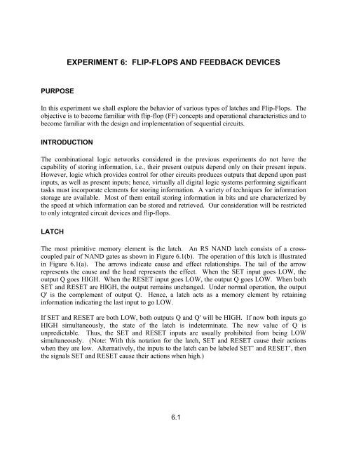
EXPERIMENT 6: FLIP-FLOPS AND FEEDBACK DEVICES<br />
PURPOSE<br />
In this <strong>experiment</strong> we shall explore the behavior of various types of latches <strong>and</strong> Flip-Flops. <strong>The</strong><br />
objective is to become familiar with <strong>flip</strong>-flop (FF) concepts <strong>and</strong> operational characteristics <strong>and</strong> to<br />
become familiar with the design <strong>and</strong> implementation of sequential circuits.<br />
INTRODUCTION<br />
<strong>The</strong> combinational logic networks considered in the previous <strong>experiment</strong>s do not have the<br />
capability of storing information, i.e., their present outputs depend only on their present inputs.<br />
However, logic which provides control for other circuits produces outputs that depend upon past<br />
inputs, as well as present inputs; hence, virtually all digital logic systems performing significant<br />
tasks must incorporate elements for storing information. A variety of techniques for information<br />
storage are available. Most of them entail storing information in bits <strong>and</strong> are characterized by<br />
the speed at which information can be stored <strong>and</strong> retrieved. Our consideration will be restricted<br />
to only integrated circuit <strong>devices</strong> <strong>and</strong> <strong>flip</strong>-<strong>flops</strong>.<br />
LATCH<br />
<strong>The</strong> most primitive memory element is the latch. An RS NAND latch consists of a crosscoupled<br />
pair of NAND gates as shown in Figure 6.1(b). <strong>The</strong> operation of this latch is illustrated<br />
in Figure 6.1(a). <strong>The</strong> arrows indicate cause <strong>and</strong> effect relationships. <strong>The</strong> tail of the arrow<br />
represents the cause <strong>and</strong> the head represents the effect. When the SET input goes LOW, the<br />
output Q goes HIGH. When the RESET input goes LOW, the output Q goes LOW. When both<br />
SET <strong>and</strong> RESET are HIGH, the output remains unchanged. Under normal operation, the output<br />
Q' is the complement of output Q. Hence, a latch acts as a memory element by retaining<br />
information indicating the last input to go LOW.<br />
If SET <strong>and</strong> RESET are both LOW, both outputs Q <strong>and</strong> Q' will be HIGH. If now both inputs go<br />
HIGH simultaneously, the state of the latch is indeterminate. <strong>The</strong> new value of Q is<br />
unpredictable. Thus, the SET <strong>and</strong> RESET inputs are usually prohibited from being LOW<br />
simultaneously. (Note: With this notation for the latch, SET <strong>and</strong> RESET cause their actions<br />
when they are low. Alternatively, the inputs to the latch can be labeled SET’ <strong>and</strong> RESET’, then<br />
the signals SET <strong>and</strong> RESET cause their actions when high.)<br />
6.1
Figure 6.1 RS NAND Latch.<br />
A simple application of the RS NAND latch is illustrated in Figure 6.2. By connecting the latch,<br />
as shown, to a switch, a contact bounce free signal is provided. This circuit output changes only<br />
once no matter how many times the switch makes <strong>and</strong> breaks contact as it bounces. <strong>The</strong> circuit<br />
is based on the assumption that TTL floating inputs act as if they were provided with HIGH<br />
inputs. <strong>The</strong> momentary breaks in contact of the switch pole with a switch terminal while the<br />
contacts are bouncing (after the switch makes initial contact) provides the circuit with floating<br />
inputs. However, since the latch remains unchanged when both inputs are HIGH, the output is<br />
unaffected by contact bounce. <strong>The</strong> circuit should be made more reliable by connecting pullup<br />
resistors to both contacts of the switch to assure that an input is a logic 1 when the switch is not<br />
connected to it.<br />
Figure 6.2 Switch Debounce Circuit.<br />
From Figure 6.2, it is clear that the latch output immediately follows changes in the inputs after<br />
one or two gate propagation delays. In this configuration, it is not possible to control the<br />
moment at which the output changes as a result of an input change. <strong>The</strong> input change alone<br />
6.2
triggers the subsequent output change. <strong>Circuits</strong> constructed from such unclocked <strong>devices</strong> as<br />
latches are referred to as asynchronous circuits. <strong>The</strong> design of asynchronous circuits is much<br />
more involved than that of synchronous circuits, in which changes of the memory element<br />
outputs are synchronized by a clock. Sequential circuit design is greatly simplified through the<br />
use of clocked <strong>flip</strong>-flop (FF) memory elements. Virtually all complex sequential systems use<br />
them. In synchronous circuits, the length of the clock period can be controlled so that when the<br />
outputs of FFs change, these changes are allowed to propagate through the combinational logic<br />
<strong>and</strong> provide stable inputs to the FFs before the next clock pulse enables the FFs to change again.<br />
Hence, any glitches in the outputs of combinational logic that may occur are not important in<br />
synchronous circuits.<br />
GATED LATCHES<br />
<strong>The</strong> gated NAND RS latch memory element is illustrated in Figure 6.3(b). (This circuit is also<br />
called a transparent latch or a latch with enable.) Its operation can be synchronized with a clock<br />
signal by connecting the gate to a clock, but by itself, it is not a clocked FF, i.e., it does not avoid<br />
many of the problems mentioned above.<br />
Figure 6.3 Gated RS Latch Controlled by a Gate Signal.<br />
6.3
From the timing diagram in Figure 6.3(a), it is seen that the outputs cannot change while the gate<br />
is LOW. <strong>The</strong> circuit acts essentially as a latch when the gate is HIGH. Hence, any changes on<br />
the inputs while the gate is HIGH will propagate to the outputs. <strong>The</strong> gate input controls the<br />
times at which the outputs may change in accordance with the R <strong>and</strong> S inputs. In this sense, its<br />
operation is synchronized by the gate. However, if we were to design a system using these gated<br />
latches all controlled by one clock connected to the gate inputs, there would be severe timing<br />
problems.<br />
Once the gated RS Latch is enabled by the clock going high, its outputs can change according to<br />
the present inputs. If the clock input is not disabled before the resulting output changes<br />
propagate through the circuit <strong>and</strong> back to the original latch inputs or to another latch controlled<br />
by the same clock, the latch outputs can change again. For predictable operation, each latch<br />
should change only once for each application of the clock. Hence, clock pulses should be long<br />
enough to enable the FF's outputs to change <strong>and</strong> yet short enough so that no output changes are<br />
permitted to propagate to latch inputs while the clock is still HIGH. Unfortunately, this is<br />
difficult to guarantee.<br />
<strong>The</strong> preceding problem can be avoided by using gated latches controlled by two-phase clock<br />
signals. In a circuit using these, the outputs from latches controlled by one phase of the clock are<br />
only allowed to propagate to latches controlled by the other phase of the clock. Hence, the<br />
inputs to a latch will not change while it is enabled. Master-Slave <strong>flip</strong>-<strong>flops</strong> are a variation of the<br />
two-phase clock approach.<br />
MASTER-SLAVE JK FLIP-FLOPS<br />
<strong>The</strong> master-slave JK <strong>flip</strong>-flop is better suited for synchronizing input changes in order to<br />
eliminate the difficulties discussed in the previous section. <strong>The</strong> master-slave JK FF is illustrated<br />
in Figure 6.4. It consists of two gated RS NAND FF's in t<strong>and</strong>em, one of which is enabled by the<br />
clock while the other is enabled by the complement of the clock. In addition, two paths feed<br />
back from the outputs to the inputs in order to generate the JK behavior.<br />
6.4
Figure 6.4 Master-slave JK FF.<br />
While the clock is LOW, the master is unaffected by any input changes. Hence, its outputs<br />
remain stable. On the other h<strong>and</strong>, the slave is enabled, <strong>and</strong> changes its state according to the<br />
master's outputs. Any output changes propagating through the circuit back to the FF inputs of<br />
the master cannot affect the FF since the master is disabled. When the clock is HIGH, the slave<br />
is disabled <strong>and</strong> the master enabled. Thus, the outputs from the slave remain stable, <strong>and</strong> hence,<br />
any slave outputs fed back to the master’s inputs remain stable.<br />
Note that while the clock is HIGH, the master functions as an enabled latch. Any momentary<br />
pulses appearing at the FF's inputs may alter its state. For example, for the slave FF output Q =<br />
0, a momentary pulse on the master's J input, while the clock is HIGH, can SET the master<br />
which was previously RESET. <strong>The</strong>re is no way to reset the master until the next clock pulse.<br />
When the clock returns LOW, the slave will subsequently be SET. For this reason, the masterslave<br />
JK <strong>flip</strong>-flop is referred to as "1's catching". No false pulses should occur on J or K while<br />
the clock is HIGH. Thus, the propagation of all signals through the logic must be completed<br />
while the clock is LOW. Also, in order to minimize the risk of corruption of circuit operation by<br />
noise, it is advisable to make the clock pulse high width as short as possible, minimizing the time<br />
the master is enabled. <strong>The</strong>se requirements lead to the use of asymmetrical clock signals <strong>and</strong><br />
limit the operational speed of the circuit.<br />
Figure 6.4 shows two additional inputs besides J, K, <strong>and</strong> the clock. <strong>The</strong> preset (PR) <strong>and</strong> clear<br />
(CLR) are asynchronous inputs which immediately set <strong>and</strong> reset the FF, respectively, regardless<br />
of the other inputs. Note that PR <strong>and</strong> CLR are active low, i.e., they cause their intended<br />
operation when they are low. Also, note that if both PR <strong>and</strong> CLR are low <strong>and</strong> return to a high<br />
value at the same time, there is a race between Q <strong>and</strong> Q′ changing to a low value, <strong>and</strong> the<br />
resulting value of Q <strong>and</strong> Q′ is determined by relative delays of the two output gates. In general,<br />
both PR <strong>and</strong> CLR should not be low at the same time.<br />
6.5
EDGE TRIGGERED FLIP-FLOPS<br />
Edge triggered <strong>flip</strong>-<strong>flops</strong> have the advantage of being sensitive to their inputs only for a short<br />
time around the rising or falling clock pulse edge, rather than throughout the entire clock pulse,<br />
as with the master-slave <strong>flip</strong>-<strong>flops</strong>. For example, the signals propagating through combinational<br />
logic to the inputs of a negative edge-triggered <strong>flip</strong>-flop need not be stabilized before the next<br />
leading positive edge of the pulse, in contrast to the case for master-slave <strong>flip</strong>-<strong>flops</strong>. Thus, a<br />
shorter clock period can be used, <strong>and</strong>, hence, faster operation is possible. In addition, the clock<br />
pulses need not be asymmetric, as with the previous <strong>flip</strong>-<strong>flops</strong>. <strong>The</strong> period during which the<br />
clock is LOW can be the same as that during which it is HIGH, without lowering the pulse<br />
frequency. This reduces the amount of circuitry required to generate the clock pulses. Since the<br />
operation of an edge-triggered <strong>flip</strong>-flop is quite complex, it will not be considered here.<br />
Figure 6.5 illustrates the operation of both a positive <strong>and</strong> negative edge triggered JK <strong>flip</strong>-flop.<br />
Figure 6.5 Positive <strong>and</strong> Negative Edge-triggered Flip-flop Behavior.<br />
Two parameters which are significant to edge-triggered <strong>flip</strong>-flop operation will be presented.<br />
Suppose we assume a negative edge triggered <strong>flip</strong>-flop. Figure 6.6 illustrates the conditions<br />
when J <strong>and</strong> K signals can change for correct operation of the <strong>flip</strong>-flop. <strong>The</strong> cross hatched areas<br />
indicate when it is permissible for J <strong>and</strong> K to change.<br />
6.6
Figure 6.6 Setup <strong>and</strong> Hold Times.<br />
<strong>The</strong> time interval for which J <strong>and</strong> K must be stable at their correct values prior to the active clock<br />
transition is the setup time, t setup . <strong>The</strong> time interval for which J <strong>and</strong> K must be stable at their<br />
correct values following the active clock transition is the hold time, t hold . It turns out that in<br />
some logic families, the signals on the J <strong>and</strong> K inputs may change before the active clock edge.<br />
In this case, the time before the active clock edge at which J <strong>and</strong> K may change is referred to as<br />
the release time, t release . <strong>The</strong>se parameters determine the maximum clock period <strong>and</strong>/or<br />
maximum number of combinational logic levels between <strong>flip</strong>-flop inputs <strong>and</strong> outputs. <strong>The</strong><br />
parameters for positive edge triggered <strong>flip</strong>-<strong>flops</strong> are found similarly.<br />
<strong>The</strong> symbols for JK <strong>flip</strong>-<strong>flops</strong> are illustrated in Figure 6.7. Note that the symbols do not<br />
distinguish the master-slave from the negative edge-triggered <strong>flip</strong>-flop. This information must<br />
be ascertained from the <strong>flip</strong>-flop's part number <strong>and</strong> data sheet. <strong>The</strong> small triangle is used to<br />
designate the clock terminal. A small circle at the clock terminal indicates that the <strong>flip</strong>-flop<br />
changes state on a negative-going signal, while the absence of the circle indicates that the state<br />
changes on a positive-going signal. Each <strong>flip</strong>-flop shown has a preset (PR) <strong>and</strong> clear (CLR)<br />
input. If PR is LOW, while CLR is HIGH, the <strong>flip</strong>-flop is set (Q changes to 1) immediately<br />
(asynchronously). If CLR is LOW, <strong>and</strong> PR is HIGH, the <strong>flip</strong>-flop is reset (Q changes to 0)<br />
immediately. Both CLR <strong>and</strong> PR LOW is forbidden. <strong>The</strong> small circles on the PR <strong>and</strong> CLR inputs<br />
indicate active LOW signals on these terminals.<br />
Figure 6.7 Flip-flop Symbols.<br />
6.7
<strong>The</strong> behavior of all three <strong>flip</strong>-<strong>flops</strong> is shown in Figure 6.8 assuming J <strong>and</strong> K are held fixed<br />
throughout the appropriate setup <strong>and</strong> hold times. <strong>The</strong> first column under CLK pertains to<br />
master-slave/negative edge-triggered FF's. <strong>The</strong> second column pertains to positive edgetriggered<br />
FF's. X indicates that the input has no effect. Z0 represents the <strong>flip</strong>-flop state prior to<br />
the activating signal, <strong>and</strong> Z1 represents the state after the activating signal.<br />
Figure 6.8 Behavior of JK Flip-<strong>flops</strong>.<br />
6.8
PRELAB<br />
1. Suppose a gated RS NOR latch is used as a clocked RS NOR FF, i.e., a clock signal is<br />
connected to the gate input. When should the R <strong>and</strong> S signals be allowed? Explain. Can you<br />
define a setup <strong>and</strong> hold time for this <strong>flip</strong>-flop as was defined for edge-triggered <strong>flip</strong>-<strong>flops</strong>? How<br />
does the clock (gate) determine these times? Should the clock pulses be HIGH for the same<br />
duration they are low? Why or why not? If not, how long should clock pulses remain HIGH?<br />
Construct such a gated RS. Use two logic level switches to provide the S <strong>and</strong> R inputs <strong>and</strong> a<br />
third to provide the gate input. <strong>The</strong> outputs may be observed on the LED's. H<strong>and</strong> in your<br />
design.<br />
2. A master-slave JK FF constructed from two gated RS NOR latches is said to be "0's<br />
catching". Explain the reason for this term <strong>and</strong> how "0's catching" can occur.<br />
3. Breadboard the circuits for Parts C <strong>and</strong> D of this <strong>experiment</strong>. Use logic level switches<br />
(toggle switches on the logic box) to provide the J, K <strong>and</strong> clock inputs for the 7476 JK masterslave<br />
<strong>flip</strong>-flop <strong>and</strong> 74LS76 JK negative edge-triggered <strong>flip</strong>-flop. Use LED's to display their<br />
outputs. H<strong>and</strong> in your designs.<br />
4. Design a circuit realizing the transition table shown below.<br />
a). Draw a transition diagram from the table.<br />
b). Using the transition table, draw next state K-maps for each <strong>flip</strong>-flop (A + , B + <strong>and</strong> C + ) <strong>and</strong><br />
obtain a minimum sum-of-products for each variable.<br />
c). Draw a schematic diagram for the state machine using three 74LS74 D-type <strong>flip</strong>-<strong>flops</strong>.<br />
Remember that when the circuit is powered-up, it needs to start in a particular state, i.e., the<br />
power-up state of the circuit cannot be r<strong>and</strong>om. Select an initial state that seems reasonable for<br />
this circuit.<br />
A B C A + B + C +<br />
0 0 0 0 1 1<br />
0 0 1 1 1 1<br />
0 1 0 1 1 0<br />
0 1 1 1 1 0<br />
1 0 0 0 0 1<br />
1 0 1 0 0 1<br />
1 1 0 1 0 0<br />
1 1 1 0 0 0<br />
6.9
PROCEDURE<br />
Before performing the procedures listed below, read the report section of the <strong>experiment</strong> to<br />
assure you make all required measurements <strong>and</strong> record all required data.<br />
A. Gated RS NOR Latch<br />
1. Connect the R, S, <strong>and</strong> gate inputs of the gated RS NOR latch, which you constructed<br />
in the prelab, to the toggle switches on the logic box. Observe the outputs on two of the<br />
logicbox LED's for the following input sequence:<br />
2. With the gate input LOW, observe the outputs on the oscilloscope for the following<br />
input sequence obtained by using a single toggle switch to supply the same signal to both R <strong>and</strong><br />
S:<br />
Does the latch always have the same output values after S <strong>and</strong> R return LOW. If so, would the<br />
outputs be the same if the S <strong>and</strong> R inputs were interchanged <strong>and</strong> the Q <strong>and</strong> Q' outputs were<br />
interchanged, i.e., if the positions of the gates were interchanged in the circuit. Name two<br />
reasons why the input combination R = 1, S=1 is usually not used on the latch?<br />
6.10
B. Master-Slave Flip-Flop<br />
1. Complete the following table using the logic box toggle switches to provide the J, K<br />
<strong>and</strong> Clock inputs to a 7476 J-K master-slave <strong>flip</strong>-flop (Note: be sure to use the 7476 FF <strong>and</strong> not<br />
the 74LS76 FF) <strong>and</strong> two logic box LED's to display the outputs:<br />
Q Q Q<br />
JK Before ↑ edge CLK While CLK = 1 After _ edge CLK<br />
00 0<br />
00 1<br />
01 0<br />
01 1<br />
10 0<br />
10 1<br />
11 0<br />
11 1<br />
2. Complete the output waveform for the following J, K, <strong>and</strong> clock inputs provided by<br />
the toggle switches on the logic box. Note that, in violation of the usual assumptions for masterslave<br />
<strong>flip</strong>-<strong>flops</strong>, the J <strong>and</strong> K inputs change while the clock is HIGH.<br />
3. This FF also has PRESET <strong>and</strong> CLEAR inputs available for asynchronous operation.<br />
In order to determine their effects, apply signals to these inputs, similar to those applied to the<br />
gated RS NOR latch. Verify that these signals override the effects of all signals applied to J, K,<br />
<strong>and</strong> the clock.<br />
C. J-K Edge Triggered Flip-Flops<br />
1. Repeat step 1 in part B for a 74LS76 JK Negative-Edge Triggered Flip-Flop. Compare<br />
the results to that obtained in part B.<br />
6.11
2. Repeat step 2 of part B for the 74LS76 FF <strong>and</strong> compare the results with that obtained<br />
in part B.<br />
D. Logic Simulation of a Sequential Circuit<br />
Enter your sequential circuit developed in the prelab into Cadence Design Entry. Simulate<br />
your circuit to verify that it behaves according to the transition table (or diagram). Correct any<br />
mistakes found. What is this circuit? <strong>The</strong> asynchronous preset <strong>and</strong> clear signals should be used<br />
to initialize the FF’s to the initial state <strong>and</strong>, after some simulation time, they should be returned<br />
high to let the FF’s operate according to the synchronous inputs.<br />
6.12
EXPERIMENT 6--FLIP-FLOPS AND FEEDBACK DEVICES<br />
FINAL REPORT<br />
I. Gated RS Latch<br />
a). Plot the response of the gated RS NOR latch you observed for the following input<br />
sequence in part A.1:<br />
Q<br />
Q'<br />
b). Plot the response of the latch observed in part A.2 for the following input sequence:<br />
Q<br />
Q'<br />
c). Does the latch always have the same output value on Q after both S <strong>and</strong> R return to 1<br />
at the same time? If so, might this change if the upper <strong>and</strong> lower gates were swapped in the<br />
circuit? Explain. Give two reasons why this latch should not be used with both inputs<br />
simultaneously 0.<br />
6.13
II. Master-Slave Flip-Flop<br />
a). Fill in the following table based on your observations of the operation of the 7476 JK<br />
master-slave FF in the lab. On the basis of this table, which input sets the device, which input<br />
resets the device, <strong>and</strong> which part of the clock pulse effects changes in the state (output) of the<br />
<strong>flip</strong>-flop.<br />
Q Q Q<br />
JK Before ↑ edge CLK While CLK = 1 After _ edge CLK<br />
00 0<br />
00 1<br />
01 0<br />
01 1<br />
10 0<br />
10 1<br />
11 0<br />
11 1<br />
b). Plot the waveforms observed for the JK master-slave <strong>flip</strong>-flop in part B.2. Do the<br />
changes on the J <strong>and</strong> K inputs, while the clock is high, affect the output?<br />
6.14
c). Based upon your observations in part B.3, what are the effects of the PRESET <strong>and</strong><br />
CLEAR lines on the 7476 FF? How are these changes affected by pulses on the J, K, <strong>and</strong> CK<br />
lines?<br />
III. J-K Edge-Triggered Flip-Flops<br />
a). Using your lab results, fill in the following table for the 74LS76 negative edgetriggered<br />
FF. How does this table compare with the corresponding table for the JK master-slave<br />
FF?<br />
Q Q Q<br />
JK Before ↑ edge CLK While CLK = 1 After _ edge CLK<br />
00 0<br />
00 1<br />
01 0<br />
01 1<br />
10 0<br />
10 1<br />
11 0<br />
11 1<br />
b). Show the waveforms observed for the 74LS76 <strong>flip</strong>-flop in part D.2 of the <strong>experiment</strong>.<br />
Compare this to the corresponding graph for the JK master-slave FF.<br />
6.15
IV. Sequential Circuit Simulation<br />
a). Attach a printout of your sequential circuit from Cadence Design Entry.<br />
b). Attach traces of your circuit in operation. Be sure that your printouts have been<br />
initialed by your TA.<br />
V. Conclusion<br />
Write a brief description of the operation of the various latches <strong>and</strong> <strong>flip</strong>-<strong>flops</strong> based on your<br />
laboratory observations. Compare the performance of the basic latch, the master-slave <strong>flip</strong>-flop,<br />
<strong>and</strong> the edge-triggered <strong>flip</strong>-flop. What are the advantages <strong>and</strong> disadvantages of each design?<br />
For what applications are each best suited?<br />
6.16