L4949 Multifunction Very Low Dropout Voltage Regulator
L4949 Multifunction Very Low Dropout Voltage Regulator
L4949 Multifunction Very Low Dropout Voltage Regulator

You also want an ePaper? Increase the reach of your titles
YUMPU automatically turns print PDFs into web optimized ePapers that Google loves.
The <strong>L4949</strong> is a monolithic integrated low dropout voltage<br />
regulator. Several outstanding features and auxiliary<br />
functions are implemented to meet the requirements of<br />
supplying microprocessor systems in automotive<br />
applications. Nevertheless, it is suitable also in other<br />
applications where the present functions are required. The<br />
modular approach of this device allows the use of other<br />
features and functions independently when required.<br />
<strong>Voltage</strong> <strong>Regulator</strong><br />
The voltage regulator uses an isolated Collector Vertical<br />
PNP transistor as a regulating element. With this structure,<br />
very low dropout voltage at currents up to 100 mA is<br />
obtained. The dropout operation of the standby regulator is<br />
maintained down to 3.0 V input supply voltage. The output<br />
voltage is regulated up to the transient input supply voltage of<br />
35 V. With this feature no functional interruption due to<br />
overvoltage pulses is generated.<br />
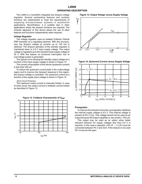
The typical curve showing the standby output voltage as a<br />
function of the input supply voltage is shown in Figure 13.<br />
The current consumption of the device (quiescent current)<br />
is less than 200 µA.<br />
To reduce the quiescent current peak in the undervoltage<br />
region and to improve the transient response in this region,<br />
the dropout voltage is controlled. The quiescent current as a<br />
function of the supply input voltage is shown in Figure 14.<br />
Short Circuit Protection:<br />
The maximum output current is internally limited. In case<br />
of short circuit, the output current is foldback current limited<br />
as described in Figure 12.<br />
<strong>L4949</strong><br />
OPERATING DESCRIPTION<br />
IQ, QUIESCENT CURRENT (mA)<br />
Vout<br />
5.0 V<br />
Figure 13. Output <strong>Voltage</strong> versus Supply <strong>Voltage</strong><br />
0 V<br />
2.0 V<br />
5.0 V<br />
Vout<br />
VCC<br />
35 V<br />
Figure 14. Quiescent Current versus Supply <strong>Voltage</strong><br />
3.0<br />
2.5<br />
2.0<br />
1.5<br />
1.0<br />
0.5<br />
TJ = 25°C<br />
RL = 100 Ω<br />
RL = 5.0 k<br />
10<br />
Figure 12. Foldback Characteristic of Vout<br />
0<br />
0 5.0 10 15 20 25 30<br />
VCC, SUPPLY VOLTAGE (V)<br />
Vout (V)<br />
5.0<br />
0<br />
20 100 200<br />
Iout (mA)<br />
Preregulator<br />
To improve the transient immunity a preregulator stabilizes<br />
the internal supply voltage to 6.0 V. This internal voltage is<br />
present at Pin 3 (VZ). This voltage should not be used as an<br />
output because the output capability is very small (≤ 100 µA).<br />
This output may be used as an option when better<br />
transient behavior for supply voltages less than 8.0 V is<br />
required. In this case a capacitor (100 nF – 1.0 µF) must be<br />
connected between Pin 3 and Gnd. If this feature is not used<br />
Pin 3 must be left open.<br />
6 MOTOROLA ANALOG IC DEVICE DATA