WM8997 - Wolfson Microelectronics plc
WM8997 - Wolfson Microelectronics plc
WM8997 - Wolfson Microelectronics plc

Create successful ePaper yourself
Turn your PDF publications into a flip-book with our unique Google optimized e-Paper software.
w<br />
<strong>WM8997</strong><br />
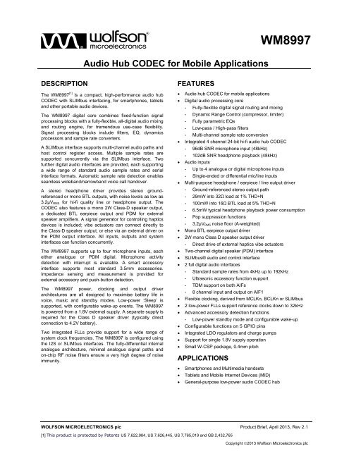
Audio Hub CODEC for Mobile Applications<br />
DESCRIPTION<br />
The <strong>WM8997</strong> [1] is a compact, high-performance audio hub<br />
CODEC with SLIMbus interfacing, for smartphones, tablets<br />
and other portable audio devices.<br />
The <strong>WM8997</strong> digital core combines fixed-function signal<br />
processing blocks with a fully-flexible, all-digital audio mixing<br />
and routing engine, for tremendous use-case flexibility.<br />
Signal processing blocks include filters, EQ, dynamics<br />
processors and sample rate converters.<br />
A SLIMbus interface supports multi-channel audio paths and<br />
host control register access. Multiple sample rates are<br />
supported concurrently via the SLIMbus interface. Two<br />
further digital audio interfaces are provided, each supporting<br />
a wide range of standard audio sample rates and serial<br />
interface formats. Automatic sample rate detection enables<br />
seamless wideband/narrowband voice call handover.<br />
A stereo headphone driver provides stereo groundreferenced<br />
or mono BTL outputs, with noise levels as low as<br />
3.2μV RMS for hi-fi quality line or headphone output. The<br />
CODEC also features a mono 2W Class-D speaker output,<br />
a dedicated BTL earpiece output and PDM for external<br />
speaker amplifiers. A signal generator for controlling haptics<br />
devices is included; vibe actuators can connect directly to<br />
the Class-D speaker output, or else via an external driver on<br />
the PDM output interface. All inputs, outputs and system<br />
interfaces can function concurrently.<br />
The <strong>WM8997</strong> supports up to four microphone inputs, each<br />
either analogue or PDM digital. Microphone activity<br />
detection with interrupt is available. A smart accessory<br />
interface supports most standard 3.5mm accessories.<br />
Impedance sensing and measurement is provided for<br />
external accessory and push-button detection.<br />
The <strong>WM8997</strong> power, clocking and output driver<br />
architectures are all designed to maximise battery life in<br />
voice, music and standby modes. Low-power ‘Sleep’ is<br />
supported, with configurable wake-up events. The <strong>WM8997</strong><br />
is powered from a 1.8V external supply. A separate supply is<br />
required for the Class D speaker driver (typically direct<br />
connection to 4.2V battery).<br />
Two integrated FLLs provide support for a wide range of<br />
system clock frequencies. The <strong>WM8997</strong> is configured using<br />
the I2S or SLIMbus interfaces. The fully-differential internal<br />
analogue architecture, minimal analogue signal paths and<br />
on-chip RF noise filters ensure a very high degree of noise<br />
immunity.<br />
FEATURES<br />
Audio hub CODEC for mobile applications<br />
Digital audio processing core<br />
- Fully-flexible digital signal routing and mixing<br />
- Dynamic Range Control (compressor, limiter)<br />
- Fully parametric EQs<br />
- Low-pass / High-pass filters<br />
- Multi-channel sample rate conversion<br />
Integrated 4 channel 24-bit hi-fi audio hub CODEC<br />
- 96dB SNR microphone input (48kHz)<br />
- 102dB SNR headphone playback (48kHz)<br />
Audio inputs<br />
- Up to 4 analogue or digital microphone inputs<br />
- Single-ended or differential mic/line inputs<br />
Multi-purpose headphone / earpiece / line output driver<br />
- Ground-referenced stereo output path<br />
- 29mW into 32Ω load at 1% THD+N<br />
- 100mW into 16Ω BTL load at 5% THD+N<br />
- 6.5mW typical headphone playback power consumption<br />
- Pop suppression functions<br />
- 3.2µV RMS noise floor (A-weighted)<br />
Mono BTL earpiece output driver<br />
2W mono Class D speaker output driver<br />
- Direct drive of external haptics vibe actuators<br />
Two-channel digital speaker (PDM) interface<br />
SLIMbus® audio and control interface<br />
2 full digital audio interfaces<br />
- Standard sample rates from 4kHz up to 192kHz<br />
- Ultrasonic accessory function support<br />
- TDM support on both AIFs<br />
- 8 channel input and output on AIF1<br />
Flexible clocking, derived from MCLKn, BCLKn or SLIMbus<br />
2 low-power FLLs support reference clocks down to 32kHz<br />
Advanced accessory detection functions<br />
- Low-power standby mode and configurable wake-up<br />
Configurable functions on 5 GPIO pins<br />
Integrated LDO regulators and charge pumps<br />
Support for single 1.8V supply operation<br />
Small W-CSP package, 0.4mm pitch<br />
APPLICATIONS<br />
Smartphones and Multimedia handsets<br />
Tablets and Mobile Internet Devices (MID)<br />
General-purpose low-power audio CODEC hub<br />
WOLFSON MICROELECTRONICS <strong>plc</strong> Product Brief, April 2013, Rev 2.1<br />
[1] This product is protected by Patents US 7,622,984, US 7,626,445, US 7,765,019 and GB 2,432,765<br />
Copyright 2013 <strong>Wolfson</strong> <strong>Microelectronics</strong> <strong>plc</strong>
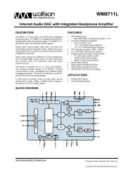
<strong>WM8997</strong><br />
BLOCK DIAGRAM<br />
Preliminary Technical Data<br />
w<br />
Product Brief, April 2013, Rev 2.1<br />
2
Preliminary Technical Data<br />
<strong>WM8997</strong><br />
TABLE OF CONTENTS<br />
DESCRIPTION ....................................................................................................... 1<br />
FEATURES ............................................................................................................ 1<br />
APPLICATIONS ..................................................................................................... 1<br />
BLOCK DIAGRAM ................................................................................................ 2<br />
TABLE OF CONTENTS ......................................................................................... 3<br />
PIN CONFIGURATION .......................................................................................... 4<br />
ORDERING INFORMATION .................................................................................. 5<br />
PIN DESCRIPTION ................................................................................................ 5<br />
ABSOLUTE MAXIMUM RATINGS ........................................................................ 7<br />
RECOMMENDED OPERATING CONDITIONS ..................................................... 8<br />
ELECTRICAL CHARACTERISTICS ..................................................................... 9<br />
TERMINOLOGY ............................................................................................................. 19<br />
DEVICE DESCRIPTION ...................................................................................... 20<br />
INTRODUCTION ............................................................................................................ 20<br />
HI-FI AUDIO CODEC ..................................................................................................... 20<br />
DIGITAL AUDIO CORE .................................................................................................. 21<br />
DIGITAL INTERFACES .................................................................................................. 21<br />
OTHER FEATURES ....................................................................................................... 22<br />
RECOMMENDED EXTERNAL COMPONENTS .................................................. 23<br />
PACKAGE DIMENSIONS .................................................................................... 24<br />
IMPORTANT NOTICE ......................................................................................... 25<br />
ADDRESS: ..................................................................................................................... 25<br />
REVISION HISTORY ........................................................................................... 26<br />
w<br />
Product Brief, April 2013, Rev 2.1<br />
3
<strong>WM8997</strong><br />
Preliminary Technical Data<br />
PIN CONFIGURATION<br />
w<br />
Product Brief, April 2013, Rev 2.1<br />
4
Preliminary Technical Data<br />
<strong>WM8997</strong><br />
ORDERING INFORMATION<br />
ORDER CODE TEMPERATURE<br />
RANGE<br />
PACKAGE<br />
<strong>WM8997</strong>ECS/R -40C to +85C W-CSP<br />
(Pb-free, Tape and reel)<br />
Note:<br />
Reel quantity = 5000<br />
MOISTURE<br />
SENSITIVITY LEVEL<br />
MSL1<br />
PEAK SOLDERING<br />
TEMPERATURE<br />
260C<br />
PIN DESCRIPTION<br />
A description of each pin on the <strong>WM8997</strong> is provided below.<br />
Note that, where multiple pins share a common name, these pins should be tied together on the PCB.<br />
PIN NO NAME TYPE DESCRIPTION<br />
H7 ADDR Digital Input Control interface (I2C) address select<br />
A3, B3, B5,<br />
C3, C4, C5,<br />
C6, D4, D5,<br />
D6, E1, E2,<br />
E3, E4, E5,<br />
F3, F4, H3<br />
AGND Supply Analogue ground (Return path for AVDD)<br />
G8 AIF1BCLK Digital Input / Output Audio interface 1 bit clock<br />
H10 AIF1LRCLK Digital Input / Output Audio interface 1 left / right clock<br />
J11 AIF1RXDAT Digital Input Audio interface 1 RX digital audio data<br />
H9 AIF1TXDAT Digital Output Audio interface 1 TX digital audio data<br />
J6 AIF2BCLK Digital Input / Output Audio interface 2 bit clock<br />
G4 AIF2LRCLK Digital Input / Output Audio interface 2 left / right clock<br />
H4 AIF2RXDAT Digital Input Audio interface 2 RX digital audio data<br />
J5 AIF2TXDAT Digital Output Audio interface 2 TX digital audio data<br />
B4, J3 AVDD Supply Analogue supply<br />
B7 CP1CA Analogue Output Charge pump 1 fly-back capacitor pin<br />
B8 CP1CB Analogue Output Charge pump 1 fly-back capacitor pin<br />
A8 CP1VOUTN Analogue Output Charge pump 1 negative output decoupling pin<br />
A7 CP1VOUTP Analogue Output Charge pump 1 positive output decoupling pin<br />
C9 CP2CA Analogue Output Charge pump 2 fly-back capacitor pin<br />
B9 CP2CB Analogue Output Charge pump 2 fly-back capacitor pin<br />
A9 CP2VOUT Analogue Output Charge pump 2 output decoupling pin / Supply for LDO2<br />
C8 CPGND Supply Charge pump 1 & 2 ground (Return path for CPVDD)<br />
C7 CPVDD Supply Supply for Charge Pump 1 & 2<br />
F6, F7, F8,<br />
G5<br />
DBVDD1 Supply Digital buffer (I/O) supply (core functions and Audio Interface 1)<br />
J4 DBVDD2 Supply Digital buffer (I/O) supply (for Audio Interface 2)<br />
J7 DCVDD Supply Digital core supply<br />
G11, H5 DGND Supply Digital ground<br />
(Return path for DCVDD, DBVDD1 and DBVDD2)<br />
A5 EPOUTN Analogue Output Earpiece negative output<br />
A4 EPOUTP Analogue Output Earpiece positive output<br />
G7 GPIO1 Digital Input / Output General Purpose pin GPIO1<br />
G3 GPIO2 Digital Input / Output General Purpose pin GPIO2<br />
J9 GPIO3 Digital Input / Output General Purpose pin GPIO3<br />
G6 GPIO4 Digital Input / Output General Purpose pin GPIO4<br />
F10 GPIO5 Digital Input / Output General Purpose pin GPIO5<br />
B10 HPDETL Analogue Input Headphone left (HPOUTL) sense input<br />
w<br />
Product Brief, April 2013, Rev 2.1<br />
5
<strong>WM8997</strong><br />
Preliminary Technical Data<br />
PIN NO NAME TYPE DESCRIPTION<br />
A10 HPDETR Analogue Input Headphone right (HPOUTR) sense input<br />
A11 HPOUTFB1/ Analogue Input HPOUTL and HPOUTR ground feedback pin 1/<br />
MICDET2<br />
Microphone & accessory sense input 2<br />
B6 HPOUTL Analogue Output Left headphone output<br />
A6 HPOUTR Analogue Output Right headphone output<br />
C1<br />
IN1LN/<br />
DMICCLK1<br />
Analogue Input /<br />
Digital Output<br />
Left channel negative differential MIC input /<br />
Digital MIC clock output 1<br />
C2 IN1LP Analogue Input Left channel single-ended MIC input /<br />
Left channel line input /<br />
Left channel positive differential MIC input<br />
D2<br />
IN1RN/<br />
DMICDAT1<br />
Analogue input /<br />
Digital Input<br />
Right channel negative differential MIC input /<br />
Digital MIC data input 1<br />
D3 IN1RP Analogue Input Right channel single-ended MIC input /<br />
Right channel line input /<br />
Right channel positive differential MIC input<br />
A1<br />
IN2LN/<br />
DMICCLK2<br />
Analogue Input /<br />
Digital Output<br />
Left channel negative differential MIC input /<br />
Digital MIC clock output 2<br />
A2 IN2LP Analogue Input Left channel single-ended MIC input /<br />
Left channel line input /<br />
Left channel positive differential MIC input<br />
B1<br />
IN2RN/<br />
DMICDAT2<br />
Analogue input /<br />
Digital Input<br />
Right channel negative differential MIC input /<br />
Digital MIC data input 2<br />
B2 IN2RP Analogue Input Right channel single-ended MIC input /<br />
Right channel line input /<br />
Right channel positive differential MIC input<br />
F11<br />
IRQ ¯¯¯ Digital Output Interrupt Request (IRQ) output (default is active low)<br />
D9 JACKDET Analogue Input Jack detect input<br />
E11 LDOENA Digital Input Enable pin for LDO1<br />
D11 LDOVDD Supply Supply for LDO1<br />
E10 LDOVOUT Analogue Output LDO1 output<br />
G10 MCLK1 Digital Input Master clock 1<br />
F9 MCLK2 Digital Input Master clock 2<br />
C10 MICBIAS1 Analogue Output Microphone bias 1<br />
D10 MICBIAS2 Analogue Output Microphone bias 2<br />
C11 MICBIAS3 Analogue Output Microphone bias 3<br />
B11<br />
MICDET1/ Analogue Input Microphone & accessory sense input 1/<br />
HPOUTFB2<br />
HPOUTL and HPOUTR ground feedback pin 2<br />
D1, E7, E8 MICVDD Analogue Output LDO2 output decoupling pin (generated internally by <strong>WM8997</strong>)<br />
E9<br />
RESET ¯¯¯¯¯¯ Digital Input Digital Reset input (active low)<br />
J10 SCLK Digital Input Control interface clock input<br />
H8 SDA Digital Input / Output Control interface data input and output / acknowledge output<br />
G9 SLIMCLK Digital Input / Output SLIM Bus Clock input / output<br />
H11 SLIMDAT Digital Input / Output SLIM Bus Data input / output<br />
J8 SPKCLK Digital Output Digital speaker (PDM) clock output<br />
H6 SPKDAT Digital Output Digital speaker (PDM) data output<br />
J1, J2 SPKGND Supply Speaker driver ground (Return path for SPKVDD)<br />
G2, H2 SPKOUTN Analogue Output Speaker negative output<br />
G1, H1 SPKOUTP Analogue Output Seaker positive output<br />
F1, F2 SPKVDD Supply Speaker driver supply<br />
D8 VREFC Analogue Output Bandgap reference decoupling capacitor connection<br />
w<br />
Product Brief, April 2013, Rev 2.1<br />
6
Preliminary Technical Data<br />
<strong>WM8997</strong><br />
ABSOLUTE MAXIMUM RATINGS<br />
Absolute Maximum Ratings are stress ratings only. Permanent damage to the device may be caused by continuously<br />
operating at or beyond these limits. Device functional operating limits and guaranteed performance specifications are given<br />
under Electrical Characteristics at the test conditions specified.<br />
ESD Sensitive Device. This device is manufactured on a CMOS process. It is therefore generically susceptible<br />
to damage from excessive static voltages. Proper ESD precautions must be taken during handling and storage<br />
of this device.<br />
<strong>Wolfson</strong> tests its package types according to IPC/JEDEC J-STD-020 for Moisture Sensitivity to determine acceptable storage<br />
conditions prior to surface mount assembly. These levels are:<br />
MSL1 = unlimited floor life at
<strong>WM8997</strong><br />
Preliminary Technical Data<br />
RECOMMENDED OPERATING CONDITIONS<br />
PARAMETER SYMBOL MIN TYP MAX UNIT<br />
Digital supply range (Core)<br />
See notes 3, 4, 5<br />
DCVDD<br />
(≤24.576MHz clocking)<br />
DCVDD<br />
(>24.576MHz clocking)<br />
1.14 1.2 1.9 V<br />
1.71 1.8 1.9<br />
Digital supply range (I/O) DBVDD1 1.7 1.9 V<br />
Digital supply range (I/O) DBVDD2 1.7 3.47 V<br />
LDO supply range LDOVDD 1.7 1.8 1.9 V<br />
Charge Pump supply range CPVDD 1.7 1.8 1.9 V<br />
Speaker supply range SPKVDD 2.4 5.5 V<br />
Analogue supply range AVDD 1.7 1.8 1.9 V<br />
Microphone Bias supply<br />
See note 6<br />
Ground<br />
Power supply rise time<br />
See notes 7, 8, 9<br />
MICVDD 2.375 3.0 3.6 V<br />
DGND, AGND, CPGND,<br />
SPKGND<br />
0 V<br />
All supplies 1 µs<br />
Operating temperature range T A -40 85 °C<br />
Notes:<br />
1. The grounds must always be within 0.3V of AGND.<br />
2. AVDD must be supplied before or simultaneously to DCVDD. DCVDD must not be powered if AVDD is not present.<br />
There are no other power sequencing requirements.<br />
3. An internal LDO (powered by LDOVDD) can be used to provide the DCVDD supply.<br />
4. ‘Sleep’ mode is supported when DCVDD is below the limits noted, provided AVDD and DBVDD1 are present.<br />
5. Under default conditions, digital core clocking rates above 24.576MHz are inhibited. The register-controlled clocking<br />
limit should only be raised when the applicable DCVDD voltage is present.<br />
6. An internal Charge Pump and LDO (powered by CPVDD) provide the Microphone Bias supply; the MICVDD pin should<br />
not be connected to an external supply.<br />
7. DCVDD and MICVDD minimum rise times do not apply when these domains are powered using the internal LDOs.<br />
8. The specified minimum power supply rise times assume a minimum decoupling capacitance of 100nF per pin.<br />
However, <strong>Wolfson</strong> strongly advises that the recommended decoupling capacitors are present on the PCB and that<br />
appropriate layout guidelines are observed.<br />
9. The specified minimum power supply rise times also assume a maximum PCB inductance of 10nH between<br />
decoupling capacitor and pin.<br />
w<br />
Product Brief, April 2013, Rev 2.1<br />
8
Preliminary Technical Data<br />
<strong>WM8997</strong><br />
ELECTRICAL CHARACTERISTICS<br />
Test Conditions<br />
AVDD = 1.8V,<br />
With the exception of the condition(s) noted above, the following electrical characteristics are valid across the full range of<br />
recommended operating conditions.<br />
PARAMETER SYMBOL TEST CONDITIONS MIN TYP MAX UNIT<br />
Analogue Input Signal Level (IN1L, IN1R, IN2L, IN2R)<br />
Full-scale input signal level V INFS Single-ended PGA input 0.5<br />
-6<br />
V RMS<br />
dBV<br />
Differential PGA input 1<br />
0<br />
V RMS<br />
dBV<br />
Notes:<br />
1. The full-scale input signal level changes in proportion with AVDD. For differential input, it is calculated as AVDD / 1.8.<br />
2. A 1.0V RMS differential signal equates to 0.5V RMS /-6dBV per input.<br />
3. A sinusoidal input signal is assumed.<br />
Test Conditions<br />
T A = +25 º C<br />
With the exception of the condition(s) noted above, the following electrical characteristics are valid across the full range of<br />
recommended operating conditions.<br />
PARAMETER SYMBOL TEST CONDITIONS MIN TYP MAX UNIT<br />
Analogue Input Pin Characteristics (IN1LP, IN1LN, IN1RP, IN1RN, IN2LP, IN2LN, IN2RP, IN2RN)<br />
Input resistance R IN All PGA gain settings 10 12 k<br />
Input capacitance C IN 5 pF<br />
Test Conditions<br />
The following electrical characteristics are valid across the full range of recommended operating conditions.<br />
PARAMETER SYMBOL TEST CONDITIONS MIN TYP MAX UNIT<br />
Input Programmable Gain Amplifiers (PGAs)<br />
Minimum programmable gain 0 dB<br />
Maximum programmable gain 31 dB<br />
Programmable gain step size Guaranteed monotonic 1 dB<br />
Headphone Output Programmable Gain Amplifiers (PGAs)<br />
Minimum programmable gain -12 dB<br />
Maximum programmable gain 0 dB<br />
Programmable gain step size Guaranteed monotonic 1 dB<br />
Earpiece Output Programmable Gain Amplifiers (PGAs)<br />
Minimum programmable gain -6 dB<br />
Maximum programmable gain +6 dB<br />
Programmable gain step size Guaranteed monotonic 1 dB<br />
w<br />
Product Brief, April 2013, Rev 2.1<br />
9
<strong>WM8997</strong><br />
Preliminary Technical Data<br />
Test Conditions<br />
The following electrical characteristics are valid across the full range of recommended operating conditions.<br />
PARAMETER SYMBOL TEST CONDITIONS MIN TYP MAX UNIT<br />
Line / Headphone / Earpiece Output Driver (HPOUTL, HPOUTR)<br />
Load resistance Normal operation 15 Ω<br />
Load capacitance<br />
Device survival with load<br />
applied indefinitely<br />
Load = 10kΩ,<br />
Normal Mode<br />
Load = 10kΩ,<br />
Mono Mode (BTL)<br />
0.1<br />
500 pF<br />
200<br />
Load = 16Ω 2 nF<br />
DC offset at Load Single-ended mode 0.1 0.2 mV<br />
Earpiece Output Driver (EPOUTP+EPOUTN)<br />
Differential (BTL) mode 0.2 0.5<br />
Load resistance Normal operation 15 Ω<br />
Device survival with load<br />
applied indefinitely<br />
Load capacitance Load = 10kΩ 200 pF<br />
0.1<br />
Load = 16Ω 2 nF<br />
DC offset at Load 0.2 0.5 mV<br />
Speaker Output Driver (SPKOUTP+SPKOUTN)<br />
Load resistance 3 Ω<br />
Load capacitance 200 pF<br />
DC offset at Load 5 mV<br />
SPKVDD leakage current 1 µA<br />
w<br />
Product Brief, April 2013, Rev 2.1<br />
10
Preliminary Technical Data<br />
<strong>WM8997</strong><br />
Test Conditions<br />
DBVDD1 = DBVDD2 = LDOVDD = CPVDD = AVDD = 1.8V,<br />
DCVDD = 1.2V (powered from LDO1), MICVDD = 3.0V (powered from LDO2), SPKVDD = 4.2V,<br />
T A = +25ºC, 1kHz sinusoid signal, fs = 48kHz, PGA gain = 0dB, 24-bit audio data unless otherwise stated.<br />
PARAMETER SYMBOL TEST CONDITIONS MIN TYP MAX UNIT<br />
Analogue Input Paths (INnL, INnR) to ADC (Differential Input Mode, INn_MODE = 00)<br />
Signal to Noise Ratio<br />
(A-weighted)<br />
SNR High performance mode<br />
(INn_OSR = 1)<br />
TBD 96 dB<br />
Normal mode<br />
(INn_OSR = 0)<br />
TBD 93<br />
Total Harmonic Distortion THD -1dBV input -83 TBD dB<br />
Total Harmonic Distortion Plus<br />
Noise<br />
THD+N -1dBV input -81 TBD dB<br />
Channel separation (Left/Right) TBD 100 dB<br />
Input noise floor<br />
A-weighted,<br />
PGA gain = +18dB<br />
3.2 TBD µV RMS<br />
Common mode rejection ratio CMRR PGA gain = +30dB TBD 60 dB<br />
PSRR (DBVDDn, LDOVDD,<br />
CPVDD, AVDD)<br />
PGA gain = 0dB TBD 70<br />
PSRR 100mV (peak-peak) 217Hz 80 dB<br />
100mV(peak-peak) 10kHz 70<br />
PSRR (SPKVDD) PSRR 100mV (peak-peak) 217Hz 80 dB<br />
100mV(peak-peak) 10kHz 70<br />
Analogue Input Paths (INnL, INnR) to ADC (Single-Ended Input Mode, INn_MODE = 01)<br />
PGA Gain = +6dB unless otherwise stated.<br />
Signal to Noise Ratio<br />
(A-weighted)<br />
SNR High performance mode<br />
(INn_OSR = 1)<br />
Normal mode<br />
(INn_OSR = 0)<br />
96 dB<br />
Total Harmonic Distortion THD -7dBV input -83 dB<br />
Total Harmonic Distortion Plus<br />
Noise<br />
THD+N -7dBV input -81 dB<br />
Channel separation (Left/Right) 100 dB<br />
Input noise floor<br />
PSRR (DBVDDn, LDOVDD,<br />
CPVDD, AVDD)<br />
A-weighted,<br />
PGA gain = +18dB<br />
93<br />
3.2 µV RMS<br />
PSRR 100mV (peak-peak) 217Hz 80 dB<br />
100mV(peak-peak) 10kHz 70<br />
PSRR (SPKVDD) PSRR 100mV (peak-peak) 217Hz 80 dB<br />
DAC to Line Output (HPOUTL, HPOUTR; Load = 10k, 50pF)<br />
100mV(peak-peak) 10kHz 70<br />
Full-scale output signal level V OUT 0dBFS input 1<br />
Vrms<br />
0<br />
dBV<br />
Signal to Noise Ratio SNR A-weighted TBD 102 dB<br />
Total Harmonic Distortion THD 0dBFS input -80 TBD dB<br />
Total Harmonic Distortion Plus<br />
Noise<br />
THD+N 0dBFS input -78 TBD dB<br />
Channel separation (Left/Right) TBD 95 dB<br />
Output noise floor<br />
PSRR (DBVDDn, LDOVDD,<br />
CPVDD, AVDD)<br />
A-weighted,<br />
PGA gain = 0dB<br />
7.9 TBD µV RMS<br />
PSRR 100mV (peak-peak) 217Hz 80 dB<br />
100mV (peak-peak) 10kHz 65<br />
PSRR (SPKVDD) PSRR 100mV (peak-peak) 217Hz 80 dB<br />
100mV (peak-peak) 10kHz 65<br />
w<br />
Product Brief, April 2013, Rev 2.1<br />
11
<strong>WM8997</strong><br />
Preliminary Technical Data<br />
Test Conditions<br />
DBVDD1 = DBVDD2 = LDOVDD = CPVDD = AVDD = 1.8V,<br />
DCVDD = 1.2V (powered from LDO1), MICVDD = 3.0V (powered from LDO2), SPKVDD = 4.2V,<br />
T A = +25ºC, 1kHz sinusoid signal, fs = 48kHz, PGA gain = 0dB, 24-bit audio data unless otherwise stated.<br />
PARAMETER SYMBOL TEST CONDITIONS MIN TYP MAX UNIT<br />
DAC to Headphone Output (HPOUTL, HPOUTR; R L = 32)<br />
Maximum output power P O 0.1% THD 30 mW<br />
Signal to Noise Ratio<br />
(A-weighted)<br />
SNR<br />
High performance mode<br />
(HPOUT_OSR = 1)<br />
Normal mode<br />
(HPOUT_OSR = 0)<br />
TBD 102 dB<br />
TBD 99<br />
Total Harmonic Distortion THD P O = 20mW -80 TBD dB<br />
Total Harmonic Distortion Plus<br />
Noise<br />
THD+N P O = 20mW -78 TBD dB<br />
Total Harmonic Distortion THD P O = 5mW -80 TBD dB<br />
Total Harmonic Distortion Plus<br />
Noise<br />
THD+N P O = 5mW -78 TBD dB<br />
Channel separation (Left/Right) TBD 95 dB<br />
Output noise floor<br />
PSRR (DBVDDn, LDOVDD,<br />
CPVDD, AVDD)<br />
A-weighted,<br />
PGA gain = -12dB<br />
3.2 TBD µV RMS<br />
PSRR 100mV (peak-peak) 217Hz 80 dB<br />
100mV (peak-peak) 10kHz 65<br />
PSRR (SPKVDD) PSRR 100mV (peak-peak) 217Hz 80 dB<br />
DAC to Headphone Output (HPOUTL, HPOUTR; R L = 16)<br />
100mV (peak-peak) 10kHz 65<br />
Maximum output power P O 0.1% THD 30 mW<br />
Signal to Noise Ratio<br />
(A-weighted)<br />
SNR<br />
High performance mode<br />
(HPOUT_OSR = 1)<br />
Normal mode<br />
(HPOUTOSR = 0)<br />
TBD 102 dB<br />
TBD 98<br />
Total Harmonic Distortion THD P O = 20mW -82 TBD dB<br />
Total Harmonic Distortion Plus<br />
Noise<br />
THD+N P O = 20mW -80 TBD dB<br />
Total Harmonic Distortion THD P O = 5mW -83 TBD dB<br />
Total Harmonic Distortion Plus<br />
Noise<br />
THD+N P O = 5mW -81 TBD dB<br />
Channel separation (Left/Right) TBD TBD dB<br />
Output noise floor<br />
PSRR (DBVDDn, LDOVDD,<br />
CPVDD, AVDD)<br />
A-weighted,<br />
PGA gain = -12dB<br />
3.2 TBD µV RMS<br />
PSRR 100mV (peak-peak) 217Hz 80 dB<br />
100mV (peak-peak) 10kHz 65<br />
PSRR (SPKVDD) PSRR 100mV (peak-peak) 217Hz 80 dB<br />
100mV (peak-peak) 10kHz 65<br />
w<br />
Product Brief, April 2013, Rev 2.1<br />
12
Preliminary Technical Data<br />
<strong>WM8997</strong><br />
Test Conditions<br />
DBVDD1 = DBVDD2 = LDOVDD = CPVDD = AVDD = 1.8V,<br />
DCVDD = 1.2V (powered from LDO1), MICVDD = 3.0V (powered from LDO2), SPKVDD = 4.2V,<br />
T A = +25ºC, 1kHz sinusoid signal, fs = 48kHz, PGA gain = 0dB, 24-bit audio data unless otherwise stated.<br />
PARAMETER SYMBOL TEST CONDITIONS MIN TYP MAX UNIT<br />
DAC to Mono Headphone Output (HPOUTL, HPOUTR, Mono Mode, R L = 32 BTL)<br />
Maximum output power P O 0.1% THD 60 mW<br />
Signal to Noise Ratio<br />
(A-weighted)<br />
SNR<br />
5% THD 100<br />
High performance mode<br />
(HPOUT_OSR = 1)<br />
100 dB<br />
Total Harmonic Distortion THD P O = 50mW -71 dB<br />
Total Harmonic Distortion Plus<br />
Noise<br />
THD+N P O = 50mW -69 dB<br />
Total Harmonic Distortion THD P O = 5mW -77 dB<br />
Total Harmonic Distortion Plus<br />
Noise<br />
THD+N P O = 5mW -75 dB<br />
Output noise floor A-weighted TBD µV RMS<br />
PSRR (DBVDDn, LDOVDD,<br />
CPVDD, AVDD)<br />
PSRR 100mV (peak-peak) 217Hz 80 dB<br />
100mV (peak-peak) 10kHz 65<br />
PSRR (SPKVDD) PSRR 100mV (peak-peak) 217Hz 80 dB<br />
DAC to Earpiece Output (EPOUTP+EPOUTN, R L = 32 BTL)<br />
100mV (peak-peak) 10kHz 65<br />
Maximum output power P O 0.1% THD 60 mW<br />
Signal to Noise Ratio<br />
(A-weighted)<br />
SNR<br />
5% THD 100<br />
High performance mode<br />
(EPOUT_OSR = 1)<br />
TBD 100 dB<br />
Total Harmonic Distortion THD P O = 50mW -71 TBD dB<br />
Total Harmonic Distortion Plus<br />
Noise<br />
THD+N P O = 50mW -69 TBD dB<br />
Total Harmonic Distortion THD P O = 5mW -77 TBD dB<br />
Total Harmonic Distortion Plus<br />
Noise<br />
THD+N P O = 5mW -75 TBD dB<br />
Output noise floor A-weighted TBD TBD µV RMS<br />
PSRR (DBVDDn, LDOVDD,<br />
CPVDD, AVDD)<br />
PSRR 100mV (peak-peak) 217Hz 80 dB<br />
100mV (peak-peak) 10kHz 65<br />
PSRR (SPKVDD) PSRR 100mV (peak-peak) 217Hz 80 dB<br />
DAC to Earpiece Output (EPOUTP+EPOUTN, R L = 16 BTL)<br />
100mV (peak-peak) 10kHz 65<br />
Maximum output power P O 0.1% THD 60 mW<br />
Signal to Noise Ratio<br />
(A-weighted)<br />
SNR<br />
10% THD 115<br />
High performance mode<br />
(EPOUT_OSR = 1)<br />
TBD 102 dB<br />
Total Harmonic Distortion THD P O = 5mW -77 TBD dB<br />
Total Harmonic Distortion Plus<br />
Noise<br />
THD+N P O = 5mW -75 TBD dB<br />
Output noise floor A-weighted TBD TBD µV RMS<br />
PSRR (DBVDDn, LDOVDD,<br />
CPVDD, AVDD)<br />
PSRR 100mV (peak-peak) 217Hz 80 dB<br />
100mV (peak-peak) 10kHz 65<br />
PSRR (SPKVDD) PSRR 100mV (peak-peak) 217Hz 80 dB<br />
100mV (peak-peak) 10kHz 65<br />
w<br />
Product Brief, April 2013, Rev 2.1<br />
13
<strong>WM8997</strong><br />
Preliminary Technical Data<br />
Test Conditions<br />
DBVDD1 = DBVDD2 = LDOVDD = CPVDD = AVDD = 1.8V,<br />
DCVDD = 1.2V (powered from LDO1), MICVDD = 3.0V (powered from LDO2), SPKVDD = 4.2V,<br />
T A = +25ºC, 1kHz sinusoid signal, fs = 48kHz, PGA gain = 0dB, 24-bit audio data unless otherwise stated.<br />
PARAMETER SYMBOL TEST CONDITIONS MIN TYP MAX UNIT<br />
DAC to Speaker Output (SPKOUTP+SPKOUTN, Load = 8, 22µH, BTL)<br />
Maximum output power P O SPKVDD = 5.0V,<br />
1% THD<br />
Signal to Noise Ratio<br />
(A-weighted)<br />
SNR<br />
SPKVDD = 4.2V,<br />
1% THD<br />
SPKVDD = 3.6V,<br />
1% THD<br />
High performance mode<br />
(SPKOUT_OSR = 1)<br />
1.2 W<br />
1.0<br />
0.7<br />
TBD 95 dB<br />
Total Harmonic Distortion THD P O = 1.0W -45 dB<br />
Total Harmonic Distortion Plus<br />
Noise<br />
THD+N P O = 1.0W -43 dB<br />
Total Harmonic Distortion THD P O = 0.5W -65 TBD dB<br />
Total Harmonic Distortion Plus<br />
Noise<br />
THD+N P O = 0.5W -63 TBD dB<br />
Output noise floor A-weighted 71 TBD µV RMS<br />
PSRR (DBVDDn, LDOVDD,<br />
CPVDD, AVDD)<br />
PSRR 100mV (peak-peak) 217Hz 75 dB<br />
100mV (peak-peak) 10kHz 65<br />
PSRR (SPKVDD) PSRR 100mV (peak-peak) 217Hz 75 dB<br />
DAC to Speaker Output (SPKOUTP+SPKOUTN, Load = 4, 15µH, BTL)<br />
Maximum output power P O SPKVDD = 5.0V,<br />
1% THD<br />
Signal to Noise Ratio<br />
(A-weighted)<br />
SNR<br />
100mV (peak-peak) 10kHz 65<br />
SPKVDD = 4.2V,<br />
1% THD<br />
SPKVDD = 3.6V,<br />
1% THD<br />
High performance mode<br />
(SPKOUT_OSR = 1)<br />
2 W<br />
1.8<br />
TBD<br />
95 dB<br />
Total Harmonic Distortion THD P O = 1.0W TBD dB<br />
Total Harmonic Distortion Plus<br />
Noise<br />
THD+N P O = 1.0W TBD dB<br />
Total Harmonic Distortion THD P O = 0.5W TBD dB<br />
Total Harmonic Distortion Plus<br />
Noise<br />
THD+N P O = 0.5W TBD dB<br />
Output noise floor A-weighted 71 µV RMS<br />
PSRR (DBVDDn, LDOVDD,<br />
CPVDD, AVDD)<br />
PSRR 100mV (peak-peak) 217Hz 75 dB<br />
100mV (peak-peak) 10kHz 65<br />
PSRR (SPKVDD) PSRR 100mV (peak-peak) 217Hz 75 dB<br />
100mV (peak-peak) 10kHz 65<br />
w<br />
Product Brief, April 2013, Rev 2.1<br />
14
Preliminary Technical Data<br />
<strong>WM8997</strong><br />
Test Conditions<br />
The following electrical characteristics are valid across the full range of recommended operating conditions.<br />
PARAMETER SYMBOL TEST CONDITIONS MIN TYP MAX UNIT<br />
Digital Input / Output (except DMICDATn and DMICCLKn)<br />
Digital I/O is referenced to DBVDD1 or DBVDD2.<br />
See “Recommended Operating Conditions” for the valid operating voltage range of each DBVDDn domain.<br />
Input HIGH Level V IH V DBVDDn =1.8V ±10% 0.65 <br />
V DBVDDn<br />
V<br />
V DBVDDn =3.3V ±10%<br />
0.7 <br />
V DBVDDn<br />
Input LOW Level V IL V DBVDDn =1.8V ±10% 0.35 <br />
V DBVDDn<br />
V DBVDDn =3.3V ±10%<br />
Note that digital input pins should not be left unconnected or floating.<br />
Output HIGH Level V OH I OH = 1mA 0.9 <br />
V DBVDDn<br />
0.3 <br />
V DBVDDn<br />
Output LOW Level V OL I OL = -1mA 0.1 <br />
V DBVDDn<br />
Input capacitance 10 pF<br />
Input leakage -1 1 µA<br />
Pull-up / pull-down resistance<br />
(where applicable)<br />
28 36 45 kΩ<br />
Digital Microphone Input / Output (DMICDATn and DMICCLKn)<br />
DMICDATn and DMICCLKn are each referenced to a selectable supply, V SUP , according to the INn_DMIC_SUP registers<br />
DMICDATn input HIGH Level V IH 0.65 V SUP V<br />
DMICDATn input LOW Level V IL 0.35 V SUP V<br />
DMICCLKn output HIGH Level V OH I OH = 1mA 0.8 V SUP V<br />
DMICCLKn output LOW Level V OL I OL = -1mA 0.2 V SUP V<br />
Input capacitance 10 pF<br />
Input leakage -1 1 µA<br />
SLIMbus Digital Input / Output (SLIMCLK and SLIMDAT)<br />
1.8V I/O Signalling (ie. 1.65V ≤ DBVDD1 ≤1.95V)<br />
Input LOW Level V IL TBD V<br />
Input HIGH Level V IH TBD V<br />
Output LOW Level V OL I OL = -1mA TBD V<br />
Output HIGH Level V OH I OH = 1mA TBD V<br />
Pin capacitance TBD pF<br />
General Purpose Input / Output (GPIOn)<br />
Clock output frequency<br />
GPIO pin configured as<br />
OPCLK or FLL output<br />
V<br />
V<br />
V<br />
26.5 MHz<br />
w<br />
Product Brief, April 2013, Rev 2.1<br />
15
<strong>WM8997</strong><br />
Preliminary Technical Data<br />
Test Conditions<br />
fs ≤ 48kHz<br />
With the exception of the condition(s) noted above, the following electrical characteristics are valid across the full range of<br />
recommended operating conditions.<br />
PARAMETER SYMBOL TEST CONDITIONS MIN TYP MAX UNIT<br />
ADC Decimation Filters<br />
Passband +/- 0.05dB 0 0.454 fs<br />
-6dB<br />
Passband ripple +/- 0.05 dB<br />
Stopband<br />
0.546 fs<br />
Stopband attenuation f > 0.546 fs 85 dB<br />
Signal path delay<br />
DAC Interpolation Filters<br />
Analogue input to<br />
Digital AIF output<br />
Passband +/- 0.05dB 0 0.454 fs<br />
-6dB<br />
0.5 fs<br />
2 ms<br />
Passband ripple +/- 0.05 dB<br />
Stopband<br />
0.546 fs<br />
Stopband attenuation f > 0.546 fs 85 dB<br />
Signal path delay<br />
Digital AIF input to<br />
Analogue output<br />
0.5 fs<br />
1.5 ms<br />
w<br />
Product Brief, April 2013, Rev 2.1<br />
16
Preliminary Technical Data<br />
<strong>WM8997</strong><br />
Test Conditions<br />
DBVDD1 = DBVDD2 = LDOVDD = CPVDD = AVDD = 1.8V,<br />
DCVDD = 1.2V (powered from LDO1), MICVDD = 3.0V (powered from LDO2), SPKVDD = 4.2V,<br />
T A = +25ºC, 1kHz sinusoid signal, fs = 48kHz, PGA gain = 0dB, 24-bit audio data unless otherwise stated.<br />
PARAMETER SYMBOL TEST CONDITIONS MIN TYP MAX UNIT<br />
Microphone Bias (MICBIAS1, MICBIAS2, MICBIAS3)<br />
Note - No capacitor on MICBIASn<br />
Note - In regulator mode, it is required that V MICVDD - V MICBIASn > 200mV<br />
Minimum Bias Voltage V MICBIAS Regulator mode<br />
1.5 V<br />
Maximum Bias Voltage (MICBn_BYPASS=0)<br />
2.8 V<br />
Bias Voltage output step size Load current ≤ 1.0mA<br />
0.1 V<br />
Bias Voltage accuracy -5% +5% V<br />
Bias Current<br />
Output Noise Density<br />
Integrated noise voltage<br />
Power Supply Rejection Ratio<br />
(CPVDD)<br />
Load capacitance<br />
Output discharge resistance<br />
External Accessory Detect<br />
Load impedance detection range<br />
(HPDETL or HPDETR)<br />
Load impedance detection<br />
accuracy<br />
(HPDETL or HPDETR)<br />
Load impedance detection range<br />
(MICDET1 or MICDET2)<br />
2.2kΩ (2%) MICBIAS resistor.<br />
Note these characteristics assume<br />
no other component is connected<br />
to MICDETn.<br />
Jack Detection input threshold<br />
voltage (JACKDET)<br />
Regulator mode<br />
(MICBn_BYPASS=0),<br />
V MICVDD - V MICBIAS >200mV<br />
Bypass mode<br />
(MICBn_BYPASS=1)<br />
Regulator mode<br />
(MICBn_BYPASS=0),<br />
MICBn_LVL = 4h,<br />
Load current = 1mA,<br />
Measured at 1kHz<br />
Regulator mode<br />
(MICBn_BYPASS=0),<br />
MICBn_LVL = 4h,<br />
Load current = 1mA,<br />
100Hz to 7kHz, A-weighted<br />
2.4 mA<br />
5.0<br />
100 nV/Hz<br />
5 µVrms<br />
PSRR 100mV (peak-peak) 217Hz 100 dB<br />
100mV (peak-peak) 10kHz 80<br />
Regulator mode<br />
(MICBn_BYPASS=0),<br />
MICBn_EXT_CAP=0<br />
Regulator mode<br />
(MICBn_BYPASS=0),<br />
MICBn_EXT_CAP=1<br />
MICBn_ENA=0,<br />
MICBn_DISCH=1<br />
50 pF<br />
1.8 4.7 µF<br />
5 kΩ<br />
8 128 Ω<br />
-30 +30 %<br />
for MICD_LVL[0] = 1 0 3 Ω<br />
for MICD_LVL[1] = 1 17 21<br />
for MICD_LVL[2] = 1 36 44<br />
for MICD_LVL[3] = 1 62 88<br />
for MICD_LVL[4] = 1 115 160<br />
for MICD_LVL[5] = 1 207 381<br />
for MICD_LVL[8] = 1 475 30000<br />
V JACKDET Jack insertion 0.5 x AVDD V<br />
Jack removal<br />
0.85 x AVDD<br />
w<br />
Product Brief, April 2013, Rev 2.1<br />
17
<strong>WM8997</strong><br />
Preliminary Technical Data<br />
Test Conditions<br />
DBVDD1 = DBVDD2 = LDOVDD = CPVDD = AVDD = 1.8V,<br />
DCVDD = 1.2V (powered from LDO1), MICVDD = 3.0V (powered from LDO2), SPKVDD = 4.2V,<br />
T A = +25ºC, 1kHz sinusoid signal, fs = 48kHz, PGA gain = 0dB, 24-bit audio data unless otherwise stated.<br />
PARAMETER SYMBOL TEST CONDITIONS MIN TYP MAX UNIT<br />
MICVDD Charge Pump and Regulator (CP2 and LDO2)<br />
Output voltage V MICVDD 1.7 3.0 3.3 V<br />
Programmable output voltage step<br />
size<br />
50 mV<br />
Maximum output current 8 mA<br />
Start-up time 4.7µF on MICVDD 1.5 3 ms<br />
Frequency Locked Loop (FLL1, FLL2)<br />
Output frequency 13 52 MHz<br />
Lock Time<br />
RESET pin Input<br />
RESET input pulse width<br />
(To trigger a Hardware Reset, the<br />
RESET input must be asserted for<br />
longer than this duration)<br />
F REF = 32kHz,<br />
F OUT = 24.576MHz<br />
F REF = 12MHz,<br />
F OUT = 24.576MHz<br />
TBD<br />
TBD<br />
ms<br />
1 µs<br />
Test Conditions<br />
The following electrical characteristics are valid across the full range of recommended operating conditions.<br />
PARAMETER SYMBOL TEST CONDITIONS MIN TYP MAX UNIT<br />
Device Reset Thresholds<br />
AVDD Reset Threshold V AVDD 0.50 1.51 V<br />
DCVDD Reset Threshold V DCVDD 0.59 0.81 V<br />
DBVDD1 Reset Threshold V DBVDD1 0.50 1.51 V<br />
Note that the reset thresholds are derived from simulations only, across all operational and process corners.<br />
Device performance is not assured outside the voltage ranges defined in the “Recommended Operating Conditions” section. Refer<br />
to this section for the <strong>WM8997</strong> power-up sequencing requirements.<br />
w<br />
Product Brief, April 2013, Rev 2.1<br />
18
Preliminary Technical Data<br />
<strong>WM8997</strong><br />
TERMINOLOGY<br />
1. Signal-to-Noise Ratio (dB) – SNR is a measure of the difference in level between the maximum full scale output signal<br />
and the output with no input signal applied. (Note that this is measured without any mute function enabled.)<br />
2. Total Harmonic Distortion (dB) – THD is the ratio of the RMS sum of the harmonic distortion products in the specified<br />
bandwidth (see note below) relative to the RMS amplitude of the fundamental (ie. test frequency) output.<br />
3. Total Harmonic Distortion plus Noise (dB) – THD+N is the ratio of the RMS sum of the harmonic distortion products<br />
plus noise in the specified bandwidth (see note below) relative to the RMS amplitude of the fundamental (ie. test<br />
frequency) output.<br />
4. Power Supply Rejection Ratio (dB) - PSRR is the ratio of a specified power supply variation relative to the output<br />
signal that results from it. PSRR is measured under quiescent signal path conditions.<br />
5. Common Mode Rejection Ratio (dB) – CMRR is the ratio of a specified input signal (applied to both sides of a<br />
differential input), relative to the output signal that results from it.<br />
6. Channel Separation (L/R) (dB) – left-to-right and right-to-left channel separation is the difference in level between the<br />
active channel (driven to maximum full scale output) and the measured signal level in the idle channel at the test<br />
signal frequency. The active channel is configured and supplied with an appropriate input signal to drive a full scale<br />
output, with signal measured at the output of the associated idle channel.<br />
7. Multi-Path Crosstalk (dB) – is the difference in level between the output of the active path and the measured signal<br />
level in the idle path at the test signal frequency. The active path is configured and supplied with an appropriate input<br />
signal to drive a full scale output, with signal measured at the output of the specified idle path.<br />
8. Mute Attenuation – This is a measure of the difference in level between the full scale output signal and the output with<br />
mute applied.<br />
9. All performance measurements are specified with a 20kHz low pass ‘brick-wall’ filter and, where noted, an A-weighted<br />
filter. Failure to use these filters will result in higher THD and lower SNR readings than are found in the Electrical<br />
Characteristics. The low pass filter removes out of band noise.<br />
w<br />
Product Brief, April 2013, Rev 2.1<br />
19
<strong>WM8997</strong><br />
Preliminary Technical Data<br />
DEVICE DESCRIPTION<br />
INTRODUCTION<br />
The <strong>WM8997</strong> is a high-performance audio hub CODEC optimised for mobile telephony and portable<br />
devices. It provides flexible, high-performance audio interfacing for handheld devices in a small and<br />
cost-effective package. It is optimised for the needs of multimedia phones using SLIMbus application<br />
processors.<br />
The <strong>WM8997</strong> digital core provides configurable capability for signal processing algorithms, including<br />
parametric equalisation (EQ) and dynamic range control (DRC). Highly flexible digital mixing,<br />
including stereo full-duplex isochronous sample rate conversion, provides use-case flexibility across a<br />
broad range of system architectures. A signal generator for controlling haptics vibe actuators is<br />
included.<br />
The <strong>WM8997</strong> provides multiple digital audio interfaces, including SLIMbus, in order to provide fully<br />
independent connections to different processors (eg. application processor, baseband processor and<br />
wireless transceiver).<br />
A flexible clocking arrangement supports a wide variety of external clock references, including<br />
clocking derived from the digital audio interface. Two integrated Frequency Locked Loop (FLL)<br />
circuits provide additional flexibility.<br />
Unused circuitry can be disabled under software control, in order to save power; low leakage currents<br />
enable extended standby/off time in portable battery-powered applications. Configurable ‘Wake-Up’<br />
actions can be associated with the low-power standby (Sleep) mode.<br />
Versatile GPIO functionality is provided, and support for external accessory / push-button detection<br />
inputs. Comprehensive Interrupt (IRQ) logic and status readback are also provided.<br />
HI-FI AUDIO CODEC<br />
The <strong>WM8997</strong> is a high-performance low-power audio CODEC which uses a simple analogue<br />
architecture. 4 ADCs and 4 DACs are incorporated, providing a dedicated ADC for each input and a<br />
dedicated DAC for each output channel.<br />
The analogue outputs comprise a 30mW (102dB SNR) stereo headphone amplifier with groundreferenced<br />
output, a 100mW differential (BTL) earpiece driver, and a Class D mono speaker driver<br />
capable of delivering 2W into a 4Ω load. Four analogue inputs are provided, each supporting singleended<br />
or differential input modes. In differential mode, the input path SNR is 96dB. The ADC input<br />
paths can be bypassed, supporting up to 4 channels of digital microphone input.<br />
The audio CODEC is controlled directly via register access. The simple analogue architecture,<br />
combined with the integrated tone generator, enables simple device configuration and testing,<br />
minimising debug time and reducing software effort.<br />
The <strong>WM8997</strong> output drivers are designed to support as many different system architectures as<br />
possible. Each output has a dedicated DAC which allows mixing, equalisation, filtering, gain and other<br />
audio processing to be configured independently for each channel. This allows each signal path to be<br />
individually tailored for the load characteristics. All outputs have integrated pop and click suppression<br />
features.<br />
The headphone output drivers are ground-referenced, powered from an integrated charge pump,<br />
enabling high quality, power efficient headphone playback without any requirement for DC blocking<br />
capacitors. Ground loop feedback is incorporated, providing rejection of noise on the ground<br />
connections. A mono mode is available on the headphone outputs; this configures the drivers as<br />
differential (BTL) outputs, suitable for an earpiece or hearing aid coil.<br />
The Class D speaker driver delivers excellent power efficiency. High PSRR, low leakage and<br />
optimised supply voltage ranges enable powering from switching regulators or directly from the<br />
battery. Battery current consumption is minimised across a wide variety of voice communication and<br />
multimedia playback use cases.<br />
w<br />
Product Brief, April 2013, Rev 2.1<br />
20
Preliminary Technical Data<br />
<strong>WM8997</strong><br />
The <strong>WM8997</strong> is cost-optimised for a wide range of mobile phone applications, and features a single<br />
channel of Class D power amplification. For applications requiring more than one channel of power<br />
amplification (or when using the integrated Class D path to drive a haptics actuator), the PDM output<br />
channels can be used to drive two external PDM-input speaker drivers. In applications where stereo<br />
loudspeakers are physically widely separated, the PDM outputs can ease layout and EMC by<br />
avoiding the need to run the Class-D speaker outputs over long distances and interconnects.<br />
DIGITAL AUDIO CORE<br />
The <strong>WM8997</strong> uses a core architecture based on all-digital signal routing, making digital audio effects<br />
available on all signal paths, regardless of whether the source data input is analogue or digital. The<br />
digital mixing desk allows different audio effects to be applied simultaneously on many independent<br />
paths, whilst also supporting a variety of sample rates concurrently. This helps support many new<br />
audio use-cases. Soft mute and un-mute control allows smooth transitions between use-cases<br />
without interrupting existing audio streams elsewhere.<br />
Highly flexible digital mixing, including mixing between audio interfaces, is possible. The <strong>WM8997</strong><br />
performs stereo full-duplex isochronous sample rate conversion, providing use-case flexibility across<br />
a broad range of system architectures. Automatic sample rate detection is provided, enabling<br />
seamless wideband/narrowband voice call handover.<br />
Dynamic Range Controller (DRC) functions are available for optimising audio signal levels. In<br />
playback modes, the DRC can be used to maximise loudness, while limiting the signal level to avoid<br />
distortion, clipping or battery droop, in particular for high-power output drivers such as speaker<br />
amplifiers. In record modes, the DRC assists in applications where the signal level is unpredictable.<br />
The 5-band parametric equaliser (EQ) functions can be used to compensate for the frequency<br />
characteristics of the output transducers. EQ functions can be cascaded to provide additional<br />
frequency control. Programmable high-pass and low-pass filters are also available for general filtering<br />
applications such as removal of wind and other low-frequency noise.<br />
DIGITAL INTERFACES<br />
Two serial digital audio interfaces (AIFs) each support PCM, TDM and I2S data formats for<br />
compatibility with most industry-standard chipsets. AIF1 supports eight input/output channels; AIF2<br />
supports two input/output channels. Bidirectional operation at sample rates up to 192kHz is<br />
supported.<br />
Four digital PDM input channels are available (two stereo interfaces); these are typically used for<br />
digital microphones, powered from the integrated MICBIAS power supply regulators. Two PDM output<br />
channels are also available (one stereo interface); these are typically used for external power<br />
amplifiers. Embedded mute codes provide a control mechanism for external PDM-input devices.<br />
The <strong>WM8997</strong> features a MIPI-compliant SLIMbus interface, providing eight channels of audio<br />
input/output. Mixed audio sample rates are supported on the SLIMbus interface. The SLIMbus<br />
interface also supports read/write access to the <strong>WM8997</strong> control registers.<br />
The <strong>WM8997</strong> is equipped with an I2C slave port (at up to 1MHz). Full access to the register map is<br />
also provided via the SLIMbus port.<br />
w<br />
Product Brief, April 2013, Rev 2.1<br />
21
<strong>WM8997</strong><br />
Preliminary Technical Data<br />
OTHER FEATURES<br />
The <strong>WM8997</strong> incorporates two 1kHz tone generators which can be used for ‘beep’ functions through<br />
any of the audio signal paths. The phase relationship between the two generators is configurable,<br />
providing flexibility in creating differential signals, or for test scenarios.<br />
A white noise generator is provided, which can be routed within the digital core. The noise generator<br />
can provide ‘comfort noise’ in cases where silence (digital mute) is not desirable.<br />
Two Pulse Width Modulation (PWM) signal generators are incorporated. The duty cycle of each PWM<br />
signal can be modulated by an audio source, or can be set to a fixed value using a control register<br />
setting. The PWM signal generators can be output directly on a GPIO pin.<br />
The <strong>WM8997</strong> provides 5 GPIO pins, supporting selectable input/output functions for interfacing,<br />
detection of external hardware, and to provide logic outputs to other devices. Comprehensive<br />
Interrupt (IRQ) functionality is also provided for monitoring internal and external event conditions.<br />
A signal generator for controlling haptics devices is included, compatible with both Eccentric Rotating<br />
Motor (ERM) and Linear Resonant Actuator (LRA) haptic devices. The haptics signal generator is<br />
highly configurable, and can execute programmable drive event profiles, including reverse drive<br />
control. An external vibe actuator can be driven directly by the Class D speaker output.<br />
The <strong>WM8997</strong> can be powered from a 1.8V external supply. A separate supply (4.2V) is typically<br />
required for the Class D speaker driver. Integrated Charge Pump and LDO Regulators circuits are<br />
used to generate supply rails for internal functions and to support powering or biasing of external<br />
microphones.<br />
A smart accessory interface is included, supporting most standard 3.5mm accessories. Jack<br />
detection, accessory sensing and impedance measurement is provided, for external accessory and<br />
push-button detection. Accessory detection can be used as a ‘Wake-Up’ trigger from low-power<br />
standby. Microphone activity detection with interrupt is also available.<br />
System clocking can be derived from the MCLK1 or MCLK2 input pins. Alternatively, the SLIMbus<br />
interface, or the audio interfaces (configured in Slave mode), can be used to provide a clock<br />
reference. Two integrated Frequency Locked Loop (FLL) circuits provide support for a wide range of<br />
clocking configurations, including the use of a 32kHz input clock reference.<br />
w<br />
Product Brief, April 2013, Rev 2.1<br />
22
Preliminary Technical Data<br />
RECOMMENDED EXTERNAL COMPONENTS<br />
<strong>WM8997</strong><br />
w<br />
Product Brief, April 2013, Rev 2.1<br />
23
<strong>WM8997</strong><br />
Preliminary Technical Data<br />
PACKAGE DIMENSIONS<br />
w<br />
Product Brief, April 2013, Rev 2.1<br />
24
Preliminary Technical Data<br />
<strong>WM8997</strong><br />
IMPORTANT NOTICE<br />
<strong>Wolfson</strong> <strong>Microelectronics</strong> <strong>plc</strong> (“<strong>Wolfson</strong>”) products and services are sold subject to <strong>Wolfson</strong>’s terms and conditions of sale,<br />
delivery and payment supplied at the time of order acknowledgement.<br />
<strong>Wolfson</strong> warrants performance of its products to the specifications in effect at the date of shipment. <strong>Wolfson</strong> reserves the<br />
right to make changes to its products and specifications or to discontinue any product or service without notice. Customers<br />
should therefore obtain the latest version of relevant information from <strong>Wolfson</strong> to verify that the information is current.<br />
Testing and other quality control techniques are utilised to the extent <strong>Wolfson</strong> deems necessary to support its warranty.<br />
Specific testing of all parameters of each device is not necessarily performed unless required by law or regulation.<br />
In order to minimise risks associated with customer applications, the customer must use adequate design and operating<br />
safeguards to minimise inherent or procedural hazards. <strong>Wolfson</strong> is not liable for applications assistance or customer<br />
product design. The customer is solely responsible for its selection and use of <strong>Wolfson</strong> products. <strong>Wolfson</strong> is not liable for<br />
such selection or use nor for use of any circuitry other than circuitry entirely embodied in a <strong>Wolfson</strong> product.<br />
<strong>Wolfson</strong>’s products are not intended for use in life support systems, appliances, nuclear systems or systems where<br />
malfunction can reasonably be expected to result in personal injury, death or severe property or environmental damage.<br />
Any use of products by the customer for such purposes is at the customer’s own risk.<br />
<strong>Wolfson</strong> does not grant any licence (express or implied) under any patent right, copyright, mask work right or other<br />
intellectual property right of <strong>Wolfson</strong> covering or relating to any combination, machine, or process in which its products or<br />
services might be or are used. Any provision or publication of any third party’s products or services does not constitute<br />
<strong>Wolfson</strong>’s approval, licence, warranty or endorsement thereof. Any third party trade marks contained in this document<br />
belong to the respective third party owner.<br />
Reproduction of information from <strong>Wolfson</strong> datasheets is permissible only if reproduction is without alteration and is<br />
accompanied by all associated copyright, proprietary and other notices (including this notice) and conditions. <strong>Wolfson</strong> is<br />
not liable for any unauthorised alteration of such information or for any reliance placed thereon.<br />
Any representations made, warranties given, and/or liabilities accepted by any person which differ from those contained in<br />
this datasheet or in <strong>Wolfson</strong>’s standard terms and conditions of sale, delivery and payment are made, given and/or<br />
accepted at that person’s own risk. <strong>Wolfson</strong> is not liable for any such representations, warranties or liabilities or for any<br />
reliance placed thereon by any person.<br />
ADDRESS:<br />
<strong>Wolfson</strong> <strong>Microelectronics</strong> <strong>plc</strong><br />
26 Westfield Road<br />
Edinburgh<br />
EH11 2QB<br />
United Kingdom<br />
Tel :: +44 (0)131 272 7000<br />
Fax :: +44 (0)131 272 7001<br />
Email :: sales@wolfsonmicro.com<br />
w<br />
Product Brief, April 2013, Rev 2.1<br />
25
<strong>WM8997</strong><br />
Preliminary Technical Data<br />
REVISION HISTORY<br />
DATE REV DESCRIPTION OF CHANGES PAGE CHANGED BY<br />
15/09/11 1.0 Customer preview under NDA MP<br />
19/10/11 1.1 Detailed description of haptics capabilities added,<br />
Pin names corrected<br />
24/10/11 1.2 I/O feature set updated,<br />
Pin names updated<br />
11/11/11 1.3 Removed DACVDD MP<br />
7/12/11 1.4 Updated power pins to reflect implementation, and block diagram to<br />
match.<br />
Updated filter spec delay wording<br />
17/02/12 1.5 Updates to all sections, and alignment with datasheet standards. PH<br />
04/07/12 1.5 Review feedback incorporated; Package Diagram updated. PH<br />
06/08/12 1.6 Package Diagram updated to DM122C - dimensions showing at top<br />
of Package Diagram corrected.<br />
08/08/12 1.6 Pin Descriptions updated to show single-ended analogue input is on<br />
the INxP pins (not INxN).<br />
MP<br />
MP<br />
MP<br />
JMacD<br />
24/09/12 2.0 Product status updated to Preliminary Technical Data JMacD<br />
24/09/12 2.0 Updates made to Electrical Characteristics PH<br />
14/12/12 2.1 Block diagram update, showing gain in AEC Loopback path PH<br />
PH<br />
w<br />
Product Brief, April 2013, Rev 2.1<br />
26