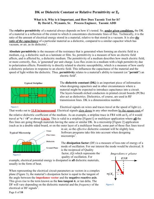
DK or Dielectric Constant or Relative Permittivity or Er - Taconic
DK or Dielectric Constant or Relative Permittivity or Er - Taconic
DK or Dielectric Constant or Relative Permittivity or Er - Taconic

Create successful ePaper yourself
Turn your PDF publications into a flip-book with our unique Google optimized e-Paper software.
<strong>DK</strong> <strong>or</strong> <strong>Dielectric</strong> <strong>Constant</strong> <strong>or</strong> <strong>Relative</strong> <strong>Permittivity</strong> <strong>or</strong> r<br />
What is it, Why is it Imp<strong>or</strong>tant, and How Does <strong>Taconic</strong> Test f<strong>or</strong> It?<br />
By David L. Wynants, Sr. Process Engineer, <strong>Taconic</strong> ADD<br />
The relative permittivity of a material always depends on how it’s tested. So, under given conditions, the <strong>DK</strong><br />
of a material is a reflection of the extent to which it concentrates electrostatic lines of flux. Technically, it is the<br />
ratio of the amount of electrical energy st<strong>or</strong>ed in a material, relative to that st<strong>or</strong>ed in a vacuum. It is also the<br />
ratio of the capacitance of a particular material as a dielectric, compared to a similar capacit<strong>or</strong> which has<br />
vacuum, <strong>or</strong> air, as its dielectric 1 .<br />
Absolute permittivity is the measure of the resistance that is generated when f<strong>or</strong>ming an electric field in a<br />
medium, e.g, a dielectric such as a laminate <strong>or</strong> film. So, permittivity is a measure of how an electric field<br />
affects, and is affected by, a dielectric medium. The permittivity of a medium describes how much electric field,<br />
<strong>or</strong> m<strong>or</strong>e c<strong>or</strong>rectly, flux, is 'generated' per unit charge. Less flux exists in a medium with a high permittivity due<br />
to polarization effects. <strong>Permittivity</strong> is directly related to electric susceptibility, which is a measure of how easily<br />
a dielectric polarizes in response to an electric field. This influences the capacitance of the material and the<br />
speed of light within the dielectric. Thus, permittivity relates to a material's ability to transmit (<strong>or</strong> "permit") an<br />
electric field 2 .<br />
The dielectric constant (<strong>DK</strong>) is an imp<strong>or</strong>tant piece of inf<strong>or</strong>mation<br />
when designing capacit<strong>or</strong>s and in other circumstances where a<br />
material might be expected to introduce capacitance into a circuit.<br />
The layers beneath etched conduct<strong>or</strong>s in printed circuit boards (PCBs)<br />
also act as dielectrics. <strong>Dielectric</strong>s, of course, are used in RF<br />
transmission lines. <strong>DK</strong> is a dimensionless number.<br />
Figure 1<br />
Electrical signals on wires and traces travel at the speed of light (c).<br />
That w<strong>or</strong>ks out to 11.8 in/nanosecond. Electrical signals slow down in any other medium by the square root of<br />
the relative dielectric coefficient of the medium. As an example, a stripline trace in FR4 with an r of 4 would<br />
travel at “c / √4” <strong>or</strong> about 6 in/ns. This is valid in a stripline [Figure1] <strong>or</strong> multilayer application where all the<br />
flux lines are going through materials having the same <strong>or</strong> similar <strong>DK</strong>. In a microstrip [Figure 2] application<br />
(such as in a double sided board, <strong>or</strong> on the outer layer of a multilayer board), some part of those flux lines travel<br />
in air, so the effective dielectric constant will be slightly less.<br />
Software programs take this into account when designing<br />
microstrips 3 .<br />
The dissipation fact<strong>or</strong> (DF) is a measure of loss-rate of energy of a<br />
mode of oscillation. F<strong>or</strong> our interest the mode would be electrical. It<br />
is the reciprocal of Quality<br />
fact<strong>or</strong>, (Q) which represents the<br />
Figure 2<br />
quality of oscillation. F<strong>or</strong><br />
example, electrical potential energy is dissipated in all dielectric materials,<br />
usually in the f<strong>or</strong>m of heat.<br />
When representing the electrical circuit parameters as vect<strong>or</strong>s in a complex<br />
plane (Figure 3), the material’s dissipation fact<strong>or</strong> is equal to the tangent of<br />
the angle between the impedance vect<strong>or</strong> and the negative reactive axis.<br />
This gives rise to the term known as the loss tangent δ, <strong>or</strong> tan delta. The<br />
DF will vary depending on the dielectric material and the frequency of the<br />
electrical <strong>or</strong> RF signals 4 .<br />
Page 1 of 10<br />
Figure 3
As DF is an indication of power, let’s discuss dBm (sometimes referred to as just dB) briefly. The term dBm is<br />
an abbreviation f<strong>or</strong> the power ratio in decibels (dB) of the measured power referenced to one milliwatt (mW).<br />
Microwave, radio, and fiber optic netw<strong>or</strong>ks use dBm as a convenient measure of absolute power because it has<br />
the capability to express both very large and very small values. Why? Because it is logarithmic in nature. Zero<br />
dBm equals one mW. A 3 dBm increase represents roughly doubling the power, which means that 3 dBm<br />
equals roughly 2 mW. F<strong>or</strong> a 3 dB decrease, the power is reduced by about one half, making −3 dBm equal to<br />
about 0.5 milliwatt 5 . The -3 dBm frequencies are used in determining the DF of a material in some of the test<br />
methods f<strong>or</strong> <strong>DK</strong> we’ll be discussing.<br />
Presented below are discussions of the four <strong>DK</strong> test methods we do at <strong>Taconic</strong>, Petersburgh [TP]. Three of them<br />
are IPC methods, listed as a <strong>DK</strong> test method f<strong>or</strong> all 17 legacy data sheets in IPC 4130A.<br />
Two Fluid Cell Method [@ 1 MHz] IPC-TM-650 2.5.5.3<br />
As the definition of <strong>DK</strong> is a ratio of capacitances, and this method measures capacitance, this method excels at<br />
<strong>DK</strong>. The ratios are that of an empty cell [air as the fluid] without and with the material under test (MUT), and a<br />
wet cell [Dow 200 silicone fluid] without and with the MUT. It is a destructive test since a discrete sized sample<br />
[~3X3] is required.<br />
But at 1 MHz? What’s the use? Well, if the <strong>DK</strong> of the material doesn’t change with frequency, as with PTFE,<br />
then the Two Fluid Cell test is as valid as a test at 10 GHz. In addition, the Two Fluid Cell Method is easier to<br />
perf<strong>or</strong>m, and multiple tests of the same dielectric thickness (DT) can be perf<strong>or</strong>med nearly simultaneously.<br />
Figure 4 <strong>DK</strong> & DF relationships between the Two Fluid Cell & X-Band, stripline test. These charts represent 17 years w<strong>or</strong>th of PTFE/Glass<br />
laminate testing @ TP. <strong>DK</strong>, on the top shows excellent c<strong>or</strong>relation, while the DF on the bottom has no c<strong>or</strong>relation, based on the R 2 value.<br />
Page 2 of 10
Virtually any <strong>DK</strong> can be measured using this method.<br />
Speaking of DTs: From the very thin to the very thick [~0.0001” to 0.2500”] can be tested. So the actual<br />
material that customers are buying is being tested. This is an imp<strong>or</strong>tant advantage f<strong>or</strong> <strong>Taconic</strong>.<br />
The DF, in my opinion, is w<strong>or</strong>thless however. Why? Very thin materials have an extremely high tested DF,<br />
while very thick samples with the same <strong>DK</strong> exhibit very low DFs. C<strong>or</strong>relations of measured DF between the<br />
Two Fluid Cell method and other test methods are non-existent, while the <strong>DK</strong> obtained by the Two Fluid Cell<br />
c<strong>or</strong>relates well with the other two <strong>DK</strong> test methods that IPC references on all 17 legacy slash sheets of IPC<br />
4103. Notice the excellent relationship between the <strong>DK</strong>s and the non-existent c<strong>or</strong>relation of the DFs done with<br />
the Two Fluid Cell and the X-Band test, as shown in the charts above [Figure 4].<br />
The temperature of the lab<strong>or</strong>at<strong>or</strong>y environment, <strong>or</strong> fixture, needs to be well controlled. The lab cannot get too<br />
hot <strong>or</strong> the <strong>DK</strong> will be too low. This is typical PTFE behavi<strong>or</strong>. Chilling the fixture [Figure 5, below] can<br />
remediate potential temperature issues within the lab. Some p<strong>or</strong>ous, highly filled, ceramic products can abs<strong>or</strong>b<br />
the silicone fluid and be problematic to test, since the capacitance raises as the air is displaced by the fluid,<br />
seemingly increasing the <strong>DK</strong>. Values need to be rec<strong>or</strong>ded immediately upon entry of the MUT in those<br />
instances.<br />
Figure 5 Not-to-Scale Schematic of 2-Fluid Cell fixture. Readings are taken with the cell empty, then with the MUT inserted. The MUT is taken<br />
out, the fixture is filled with Dow 200 silicone fluid. Readings are taken; the MUT is re-inserted and final readings taken. A spreadsheet spits out<br />
the <strong>DK</strong>.<br />
Here is a link to the IPC test method: http://www.ipc.<strong>or</strong>g/4.0_Knowledge/4.1_Standards/test/2.5.5.3c.pdf<br />
Full Sheet Resonance [FSR] Method [TP Stnd @ 130 to 500 MHz] IPC-TM-650 2.5.5.6<br />
FSR is a non-destructive test and faster to perf<strong>or</strong>m than the Two Fluid Cell method. Given a clean-cut sample<br />
edge, and sufficient flo<strong>or</strong> space, virtually any sized panel can be tested, from a 6X6 to an 18X102.<br />
What happens in an FSR test? A signal is launched from the output p<strong>or</strong>t of the VNA from the edge of a cut<br />
panel. The clad panel acts as a wave guide. The edges behave as “opens” and so reflect the signal back into the<br />
Page 3 of 10
panel. The <strong>DK</strong> and the panel dimension determine how the reflected signals behave inside the panel to create<br />
the resonant pattern seen on the CRT screen of the vect<strong>or</strong> netw<strong>or</strong>k analyzer (VNA).<br />
Notice the patterns, in the figures below, created by a TLX-9 & a TLX-6. They should look almost identical.<br />
But the TLX-6 is a square 12X12, while the TLX-9 is a rectangular 12X18. Square panels generally show an<br />
unambiguous, single peak [actually a “valley”] in the frequency range tested. Rectangular panels show a<br />
“noisier” wave f<strong>or</strong>m due to all the possible resonances from the uneven length sides. Note the relatively simple<br />
display of the 12X18 of the TLX-9 to the many peaks generated by the C<strong>Er</strong>-10’s 12X18 in Figure 6, below.<br />
Figure 6 CRT representations from an HP VNA #8720B showing FSR tests of 2.65, 2.5, & 9.70 [30mil] <strong>DK</strong> materials, respectively.<br />
How is the proper peak selected? Generally familiar products with a long hist<strong>or</strong>y of FSR data are being tested.<br />
However, if a different panel size <strong>or</strong> an unfamiliar <strong>DK</strong> is being measured, the expected frequencies can be<br />
generated through the use of the Mode Table file in Excel . The panel size and expected <strong>DK</strong> are entered into<br />
the Mode Table and the fist 4 modes are calculated.<br />
Figure 7 Mode Table: Generating expected frequencies.<br />
In the example shown to the left[Figure 7], a C<strong>Er</strong>-10-0250 panel<br />
with the dimensions of 18X24 and an expected <strong>DK</strong> of 9.5 shows<br />
that the first peak available in the frequency range is 213 MHz <strong>or</strong><br />
0.213 GHz. We always put the sh<strong>or</strong>ter dimension first as that is the<br />
direction that the signal will be launched into the panel. [See<br />
below] The frequency of 0.213 GHz represents the 2:0 mode. TP<br />
always chooses to measure the M (X) :0 modes since this simplifies<br />
the calculations when N=0. F<strong>or</strong> an explanation, here is a quote<br />
from the IPC procedure f<strong>or</strong> the FSR method [<br />
http://www.ipc.<strong>or</strong>g/4.0_Knowledge/4.1_Standards/test/2.5.5.6.pdf ]:<br />
“5.4 Selection of Unambiguous Resonant Modes In a conventional waveguide cavity, reflections at the metal bounded sides show a<br />
current maximum, while in the parallel plate waveguide, reflections at open edges <strong>or</strong> c<strong>or</strong>ners show a voltage maximum. When the<br />
waveguide is a rectangle, as f<strong>or</strong> clad panels, each resonance mode is a grid array pattern of maxima and may be designated (M:N),<br />
where M is the integer number of times (nodes) the pattern repeats along the length and<br />
N along the width.”<br />
<strong>Taconic</strong> uses a simplified text fixture, as seen in Figure 8, to the right. The<br />
test itself is pretty direct. After calibrating the VNA f<strong>or</strong> the FSR test, [an<br />
open response f<strong>or</strong> the S 22 parameter , which is the output p<strong>or</strong>t voltage<br />
reflection coefficient], a panel is placed in the <strong>or</strong>ientation shown. The<br />
signal launching pin is lowered down to the surface of the panel. The<br />
c<strong>or</strong>rect “valley” in the spectrum shown on the CRT screen of the VNA is<br />
chosen. The frequency of interest is then entered into an FSR spreadsheet,<br />
Figure 8 Simplified FSR Fixture<br />
where the measured dimension and mode have already been entered, and<br />
the <strong>DK</strong> value is generated. Repeat. F<strong>or</strong> thinner laminates [
How does the FSR compare to the 1 MHz test? Very well, as shown in the two charts below [Figures 9&10].<br />
Figure 9 Lab Press FSR Results vs Two Fluid Cell<br />
Figure 10 Production laminate FSR results vs Two Fluid Cell<br />
The one on the right shows TP production testing data. The chart on the left is from Lab Press panels that were<br />
FSR tested using 7X10 sample sizes. Since the 3X3 sample used f<strong>or</strong> the Two Fluid Cell test represents a much<br />
greater percentage [3X to 6X] of the<br />
<strong>or</strong>iginal FSR tested panel, the R 2 value is<br />
higher f<strong>or</strong> the Lab Press samples than the<br />
production panels.<br />
The FSR method compares well with the<br />
Bereskin method also. The graph to the left<br />
[Figure 11] shows a comparison of <strong>DK</strong><br />
values obtained by FSR and Bereskin of<br />
RF-35A.<br />
Figure 11 FSR vs Bereskin testing<br />
Figure 12 FSR tested over a range of frequencies on the same panel<br />
FSR testing has been perf<strong>or</strong>med at higher<br />
frequencies. Shown in Figure 12 is FSR<br />
data measured between 15.5 & 17.5 GHz,<br />
perf<strong>or</strong>med on a verification panel of RF-60<br />
f<strong>or</strong> the FSR test. Modes from 79 to 88,<br />
inclusive, were measured. Frequencies<br />
above 12 GHz require a different cable and<br />
recalibration to achieve a clean signal.<br />
Since the cladding remains on the dielectric,<br />
in FSR testing, unlike other tests where the<br />
cladding is removed, there are no air pockets<br />
which could lower the <strong>DK</strong> values, as is<br />
observed other test methods. So, the FSR<br />
<strong>DK</strong> value may be slightly higher than other<br />
test methods. The holes left in the surface by<br />
copper dendrites may trap microscope air<br />
pockets and lower the <strong>DK</strong> in the Two Fluid<br />
Cell test and wherever retains are<br />
“squeezed” in a test fixture such as in the X-<br />
Band & Bereskin test methods.<br />
Page 5 of 10
X-Band Test Method [@ 8 – 12 GHz] by Stripline Using a Resonant Element Pattern Card<br />
Figure 13 Resonant peak to determine <strong>DK</strong><br />
Figure 14 Schematic of X-Band fixture from IPC-TM-650 2.5.5.5<br />
Figure 15 Resonat<strong>or</strong> Pattern Card template from IPC-TM-650 2.5.5.5<br />
This is the “test” elephant in the room.<br />
Companies which sold mainly to the<br />
military market, which required, f<strong>or</strong> certain<br />
laminates, testing at X-Band, are especially<br />
attached to this method. This method can<br />
spit out a <strong>DK</strong> and an adequate DF loss<br />
number. It determines the loss based on - 3<br />
dBm from the resonant frequency [See<br />
Figure 13]. Since loss relates to power and<br />
this method is using the - 50% power from<br />
resonant, the result is valid f<strong>or</strong> this set-up.<br />
This method is often preferred because it’s<br />
in the X-Band frequency range [8 to 12.4<br />
GHz]; though the maj<strong>or</strong>ity of TP’s<br />
customers have applications are in the<br />
UHF, L, S, & C-bands [all
A drawback to this method is that the 8.5 mils of the resonat<strong>or</strong> card becomes part of the MUT. This is even<br />
mentioned in the IPC test procedure. [Limitations 1.3.3] So, if a 3.0 card is used to test a 2.95 nominal material,<br />
the <strong>DK</strong> and DF will be shifted slightly higher. Conversely, testing a 3.2 <strong>DK</strong> with the same card will pull the <strong>DK</strong><br />
and DF lower. If the <strong>DK</strong> tolerance of the product being tested is narrower than the <strong>DK</strong> tolerance of the<br />
resonat<strong>or</strong> card, materials can be rejected.<br />
Another issue is that the test is not able to accommodate all thicknesses of product that a company might offer.<br />
The specimens required are 2 pieces <strong>or</strong> sets of pieces from 58.3 to 66.9 mils thick. That is, except f<strong>or</strong> the<br />
highest <strong>DK</strong>; this requires specimen sets <strong>or</strong> pieces of 46.5 to 53.5 mils. So only DTs divisible into ~ 60 mils: 2-<br />
30s, 3-20s, 4-15 mils <strong>or</strong> f<strong>or</strong> the 10.5 <strong>DK</strong> 1-50, 2-25 mils may be tested. Period. Of course, anything thicker than<br />
the set sizes cannot be tested with this method. The procedure warns that using built-up specimens can<br />
introduce up to 5% err<strong>or</strong> due to air gaps [See the Note at the end of 3.1 under Test Specimens]. Interestingly, the<br />
old MIL-S-13949 slash sheets [Cancelled in November 1998] f<strong>or</strong> GY & GX laminates, <strong>Taconic</strong>’s TLY & TLX<br />
laminates, states that “Materials other than 0.030 and 0.060 inch thick are not testable at 10 GHz.” Theref<strong>or</strong>e, if<br />
a customer <strong>or</strong>ders, f<strong>or</strong> example, a 45 mil, <strong>or</strong> anything thicker than 67 mils, it cannot be tested with this method.<br />
The very good <strong>DK</strong> c<strong>or</strong>relation with the 2-fluid cell test was given above in Figure 4. The maj<strong>or</strong> purpose of this<br />
test method, which can be applied to any test method is stated in the procedure itself:<br />
“1.3 Limitations … Users are cautioned against assuming the method yields permittivity and loss tangent values that<br />
directly c<strong>or</strong>respond to applications. The value of the method is f<strong>or</strong> assuring consistency of product, thus reproducibility of<br />
results in fabricated boards.”<br />
Bereskin Test Method [@ ~1 to ~ 22 GHz] [Modified into IPC-TM-650 2.5.5.5.1]<br />
This method excels at DF. Why? Because: power is being measured. Power in versus power out. Even the<br />
Figure 16 Schematic of the Bereskin fixture from his patent #5,187,443; Fig.1<br />
resonant frequency is derived from the two – 3dBm points. This is unlike the X-Band test where the resonant<br />
frequency is found and used f<strong>or</strong> the <strong>DK</strong>, the Bereskin test takes the average frequency after determining the -3<br />
dBm frequencies. That average frequency is used to determine the <strong>DK</strong>. This is why Bereskin excels f<strong>or</strong> DF. The<br />
Page 7 of 10
limiting fact<strong>or</strong> f<strong>or</strong> this method is that 11 mils is the thinnest to be tested, without stacking. The 11 mil limit is<br />
due to the fringing length addition to the center copper strip [See Figure 16, above].<br />
A range of frequencies can be tested, depending on the <strong>DK</strong> and DF of the material. Low loss materials can be<br />
tested to higher frequencies. This may be due to the connect<strong>or</strong>s attached to the fixture itself. Also, the fixture<br />
currently in use [not the longer, 7” fixture, mentioned in the second patent] seems to have a self resonance<br />
around 4 GHz, obscuring measurements between ~3.7 and ~5 GHz.<br />
In the procedure, two samples [<strong>or</strong> sets] of identical thickness are placed in the test fixture under pressure with<br />
the standardized copper strip compressed in between to create an imbedded stripline resonat<strong>or</strong>. A signal is<br />
propagated [excited] through the z axis of the sample and the resonant frequency is detected by finding the most<br />
power. Using the resonant frequency found from the -3dBm points, as described above, Ε r is derived from the<br />
equation:<br />
Ε r = C / (2.54*F 0 *Leq) 2<br />
Where C= speed of light,<br />
F 0 = resonant frequency and<br />
Leq = conduct<strong>or</strong> length including field fringing.<br />
Figure 17 is the set-up showing a 26.5 GHz<br />
synthesized sweep oscillat<strong>or</strong> on the left; the two,<br />
stacked, power meters in the center; and the fixture<br />
itself in the press that applies a 200 psi f<strong>or</strong>ce, on<br />
the right. The test itself is explained in the two<br />
patents; 5,083,088 & 5,187,443 available at the<br />
USPTO website: http://patft.uspto.gov/netacgi/nph-<br />
Parser?Sect1=PTO2&Sect2=HITOFF&p=1&u=%2Fnetahtml%2FPTO%2Fs<br />
earchadv.htm&r=1&f=G&l=50&d=PALL&S1=05083088&OS=PN/05083088&R<br />
S=PN/05083088 & http://patft.uspto.gov/netacgi/nph-<br />
Parser?Sect1=PTO2&Sect2=HITOFF&p=1&u=%2Fnetahtml%2FPTO%2Fs<br />
earchadv.htm&r=1&f=G&l=50&d=PALL&S1=05187443&OS=PN/05187443&R<br />
S=PN/05187443<br />
How does this test method compare? Allied Signal<br />
Figure 17 The Bereskin set up @ TP<br />
Laminate Systems presented this discussion of the<br />
Bereskin test method at the IPC Expo ’99 in 1999 in Long Beach, CA under the tile “New Developments in<br />
High Frequency <strong>Dielectric</strong> Measurements of PWB Materials Part II: Applications of the Bereskin Method to<br />
PWB Materials.” Under the subheading<br />
“Comparison to Other Techniques” it stated:<br />
Figure 18 Charted test values f<strong>or</strong> various methods @ various frequencies<br />
Page 8 of 10<br />
“A pure polysulfone sample tested f<strong>or</strong> <strong>DK</strong> and<br />
DF at various frequencies in our lab<strong>or</strong>at<strong>or</strong>y by<br />
the Bereskin Method was also tested by the<br />
Resonant Re-Entry Cavity technique 3 at the 3M<br />
Lab<strong>or</strong>at<strong>or</strong>y 4 . These data were compared to<br />
hist<strong>or</strong>ical data obtained at MIT using a<br />
waveguide technique 5 . The results summarized<br />
in Table 3 [Figure 18, to the left], indicate very<br />
good c<strong>or</strong>relation between the Bereskin method<br />
and the other two techniques f<strong>or</strong> pure<br />
polysulfone.” [F<strong>or</strong> the footnotes in the<br />
quotation, see the <strong>or</strong>iginal paper.]
Figure 19 Graphed data from Allied Signal’s 1999 presentation at the IPC Expo in Long Beach, CA<br />
Here is the data from “Table 3” graphed, above in Figure 19, to easily see the relationship. [Polysulfone<br />
([C 27 H 22 O 4 S] n ) is a thermoplastic, without PTFE’s high temperature robustness. Polysulfone melts at 371°F!]<br />
How does the Bereskin Method<br />
compare with the other <strong>DK</strong> tests<br />
perf<strong>or</strong>med by <strong>Taconic</strong>? Data from<br />
<strong>Taconic</strong>’s internal testing is shown<br />
in Figures 20 & 21. The Bereskin<br />
<strong>DK</strong> @ 1.9 GHz displays excellent<br />
c<strong>or</strong>relation with both the X-Band<br />
and 1 MHz <strong>DK</strong>s.<br />
Figure 20 The Bereskin test method vs the X-Band & Two Fluid Cell [1 MHz] test methods<br />
The other <strong>DK</strong> test perf<strong>or</strong>med at<br />
<strong>Taconic</strong>, the FSR method, was<br />
already shown in the section<br />
devoted to that method above, as a<br />
good predict<strong>or</strong> of RF-35A <strong>DK</strong>.<br />
When graphed with the products<br />
<strong>Taconic</strong> certifies to the FSR<br />
method; the RF-41s, -43s, -45s, -<br />
60As, & Cr-10; the Bereskin<br />
method does well as seen by the<br />
high R 2 value.<br />
The Bereskin method has been<br />
used to perf<strong>or</strong>m DOA testing<br />
[Degree of Anisotropy]. The<br />
relatively small sample size, two<br />
1.1625” X 4” pieces, make testing<br />
in all three axis [X,Y, & Z] just a<br />
matter of making a suitably thick<br />
laminate 6 .<br />
These are the four <strong>DK</strong> tests<br />
perf<strong>or</strong>med at <strong>Taconic</strong>’s Advanced<br />
<strong>Dielectric</strong> Division.<br />
Figure 21 Bereskin test method vs the FSR test method<br />
Page 9 of 10
David L. Wynants, Sr. has been with <strong>Taconic</strong> f<strong>or</strong> over 35 years. He has designed<br />
<strong>or</strong> revised over 1,600 dielectric offerings of <strong>Taconic</strong> ADD since being assigned to<br />
that division. He is a f<strong>or</strong>mer supervis<strong>or</strong> of <strong>Taconic</strong>’s QA Lab, and was<br />
instrumental in bringing the Bereskin Test Method to <strong>Taconic</strong>, being trained by<br />
Dr. Alexander Bereskin himself. He is an ASQ recognized Green Belt.<br />
References:<br />
1 http://en.wikipedia.<strong>or</strong>g/wiki/<strong>Relative</strong>_permittivity<br />
2 http://en.wikipedia.<strong>or</strong>g/wiki/<strong>Permittivity</strong> , http://en.wikipedia.<strong>or</strong>g/wiki/Electric_susceptibility<br />
3 http://www.ultracad.com/ment<strong>or</strong>/microstrip%20propagation.pdf<br />
4 http://en.wikipedia.<strong>or</strong>g/wiki/Dissipation_fact<strong>or</strong><br />
5 http://en.wikipedia.<strong>or</strong>g/wiki/DBm<br />
6 \\Tpnt1\public\Keep\A.D.D\TSM-30 Anisotropy Rep<strong>or</strong>t.docx<br />
All accessed on 11.11.11.<br />
Page 10 of 10