download the PDF - Global Solar Technology
download the PDF - Global Solar Technology
download the PDF - Global Solar Technology

Create successful ePaper yourself
Turn your PDF publications into a flip-book with our unique Google optimized e-Paper software.
www.globalsolartechnology.com<br />
News for <strong>the</strong> <strong>Solar</strong> Manufacturing Industry<br />
Volume 2 Number 4 July/August 2009<br />
Dr. Madhusudan V. Atre<br />
Interview Inside<br />
The importance of Cpk<br />
Debugging and verifying microinverters<br />
for photovoltaic installationS<br />
Lasers, for more efficient solar cells<br />
NEW PRODUCTS<br />
INDUSTRY NEWS<br />
INTERNATIONAL DIARY
Contents<br />
<strong>Global</strong> <strong>Solar</strong> <strong>Technology</strong> is<br />
distributed by controlled<br />
circulation to qualified<br />
personnel. For all o<strong>the</strong>rs,<br />
subscriptions are available<br />
at a cost of £110/US<br />
$220/€165 for <strong>the</strong> current<br />
volume (6 issues).<br />
No part of this publication<br />
may be reproduced,<br />
stored in a retrieval system,<br />
transmitted in any form or<br />
by any means —electronic,<br />
mechanical, photocopying,<br />
recording or o<strong>the</strong>rwise—<br />
without <strong>the</strong> prior written<br />
consent of <strong>the</strong> publisher.<br />
No responsibility is accepted<br />
for <strong>the</strong> accuracy of<br />
information contained in<br />
<strong>the</strong> text, illustrations or advertisements.<br />
The opinions<br />
expressed in <strong>the</strong> articles are<br />
not necessarily those of <strong>the</strong><br />
editors or publisher.<br />
© Trafalgar Publications<br />
Ltd.<br />
Designed and Published<br />
by Trafalgar Publications,<br />
Bournemouth, United<br />
Kingdom<br />
Contents<br />
2 Forget oversupply; welcome <strong>the</strong> era of clean energy<br />
Debasish Choudhury<br />
<strong>Technology</strong> Focus<br />
8 Debugging and verifying microinverters for photovoltaic<br />
installations<br />
Win Seipel, Agilent Technologies, Inc., Santa Clara, CA<br />
12 The importance of Cpk<br />
Darren Brown, DEK, Weymouth, UK<br />
Special Features<br />
10 The importance of seal selection on PV productivity<br />
and cost<br />
16 Lasers, for more efficient solar cells<br />
18 Interview— Dr. Madhusudan V. Atre, Applied Materials<br />
India Pvt. Ltd.<br />
20 Intersolar lights up San Francisco<br />
22 PV America gets off to a good start in Philadelphia<br />
22 Shah demands respect for solar industry at PV America<br />
REGULAR COLUMNS<br />
6 Renewable energy going forward<br />
Dr. Jennie S. Hwang<br />
!<br />
16<br />
Volume 2, No. 4<br />
July/August 2009<br />
8<br />
18<br />
Regular Features<br />
4 Industry News<br />
24 Technological Developments<br />
28 New Products<br />
40 Events Calendar<br />
Visit <strong>the</strong> website for more news & content: www.globalsolartechnology.com.<br />
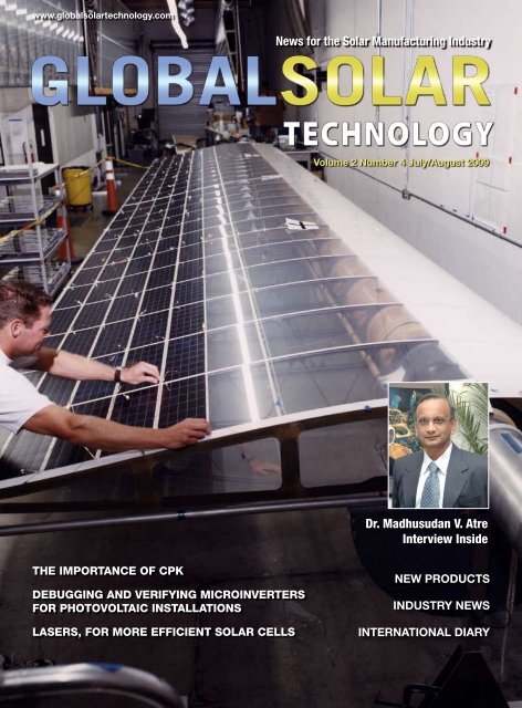
A technician lays a panel of solar<br />
cells into place on a wing section<br />
of <strong>the</strong> Helios Prototype flying<br />
wing at AeroVironment’s Design<br />
Development Center in Simi<br />
Valley, California. Source: NASA.<br />
www.globalsolartechnology.com<br />
<strong>Global</strong> <strong>Solar</strong> <strong>Technology</strong> – July/August 2009 – 1
Editorial<br />
Editorial Offices<br />
Europe<br />
<strong>Global</strong> <strong>Solar</strong> <strong>Technology</strong><br />
Trafalgar Publications Ltd<br />
8 Talbot Hill Road<br />
Bournemouth<br />
Dorset BH9 2JT<br />
United Kingdom<br />
Tel: +44 (1202) 388997<br />
news@globalsolartechnology.com<br />
www.globalsolartechnology.com<br />
United States<br />
<strong>Global</strong> <strong>Solar</strong> <strong>Technology</strong><br />
PO Box 7579<br />
Naples, FL 34102<br />
USA<br />
Tel: (239) 567-9736<br />
news@globalsolartechnology.com<br />
China<br />
<strong>Global</strong> <strong>Solar</strong> <strong>Technology</strong><br />
Electronics Second<br />
Research Institute<br />
No.159, Hepin South Road<br />
Taiyuan City, PO Box 115, Shanxi,<br />
Province 030024, China<br />
Tel: +86 (351) 652 3813<br />
Editor-in-Chief—Trevor Galbraith<br />
Tel: +44 (0)20 8123 6704 (Europe)<br />
Tel: +1 239 567 9736 (US)<br />
editor@globalsolartechnology.com<br />
Managing Editor—Hea<strong>the</strong>r Lackey<br />
hglackey@globalsolartechnology.com<br />
Editor—Debasish Choudhury<br />
Tel: +91 120 6453260<br />
dchoudhury@globalsolartechnology.com<br />
Circulation and Subscriptions<br />
Tel: +1 (239) 567 9736<br />
subscriptions@globalsolartechnology.com<br />
Advertising<br />
Print & Digital - Europe<br />
Donal McDonald<br />
Tel: +353 86 2485842<br />
dmcdonald@globalsolartechnology.<br />
com<br />
Print - North America<br />
Lino D’Andreti<br />
Tel: +1 (603) 580-5549<br />
ldandreti@globalsolartechnology.com<br />
Digital - North America<br />
Sandy Daneau<br />
Tel: +1 (603)-686-3920<br />
sdaneau@globalsolartechnology.com<br />
Asia/Pacific<br />
Print - Debasish Choudhury<br />
Tel: +91 120 6453260<br />
dchoudhury@globalsolartechnology.com<br />
Year 2008 was <strong>the</strong> golden year for <strong>the</strong><br />
global solar industry, which registered<br />
an astronomical 123% growth in PV<br />
installations, totalling to 5.2 GW<br />
worldwide, compared to 2.4 GW installed<br />
base in 2007. Then came <strong>the</strong> real shock!<br />
The Spanish government suddenly reduced<br />
<strong>the</strong> subsidy limit to 500 MW from its<br />
installation volume of 2.2GW in 2008,<br />
which was largest in <strong>the</strong> world. This<br />
single demand collapse, combined with<br />
disappointing demand due to <strong>the</strong> global<br />
economic crisis, pushed average inventories<br />
throughout <strong>the</strong> solar supply chain up by<br />
64.3%, spurring major oversupply and<br />
price erosion.<br />
The situation turned acute in <strong>the</strong> first<br />
quarter of 2009, when <strong>the</strong> average days of<br />
inventory across <strong>the</strong> solar production value<br />
chain surged to more than 121, up from<br />
74.2 during <strong>the</strong> same period in 2008.<br />
China, which saw <strong>the</strong> enormous<br />
growth of its solar photovoltaic industry in<br />
2008, found <strong>the</strong> big behemoths scouring<br />
for cover a year later. The Chinese<br />
government acted swiftly, and announced<br />
a new $2.70 per watt government solar<br />
incentive program, which provided a strong<br />
impetus to local solar stocks, representing a<br />
50% government participation in <strong>the</strong> cost<br />
of many Chinese solar projects.<br />
The Japan government expressed its<br />
intention to renew <strong>the</strong>ir solar subsidy<br />
program earlier this year as well, post its<br />
closure in 2006.<br />
Thanks to U.S. President Barack<br />
Obama’s American Recovery and<br />
Reinvestment Act of 2009, gradually, <strong>the</strong><br />
clean energy program became a buzz word<br />
around <strong>the</strong> globe.<br />
India’s ancient scriptures speak of<br />
“Ekham Adityam”—<strong>the</strong> one Sun as <strong>the</strong><br />
source of inexhaustible energy. The<br />
National <strong>Solar</strong> Mission, set up as part of<br />
Debasish Choudhury<br />
Editor, <strong>Global</strong> <strong>Solar</strong> <strong>Technology</strong><br />
Forget oversupply; welcome<br />
<strong>the</strong> era of clean energy<br />
<strong>the</strong> Prime Minister’s National Action Plan<br />
on Climate Change (NAPCC) in 2008, is<br />
reported to be targeting generation of 20<br />
GW solar power by 2020, from <strong>the</strong> current<br />
miniscule level of 2.2 MW. The mission<br />
also reported to have set up ambitious<br />
target’s of 100 GW solar power by 2030,<br />
and 200 GW solar power by 2050. There<br />
is a strong possibility of this mission’s<br />
announcement by India government in<br />
mid August.<br />
If <strong>the</strong>se announcements weren’t<br />
enough to inflate <strong>the</strong> mood of <strong>the</strong> global<br />
solar industry, <strong>the</strong>n came this earthshattering<br />
announcement: Desertec<br />
Industrial Initiative (DII). The project,<br />
promoted by twelve leading international<br />
solar companies and sponsored by<br />
Germany’s Munich Re, plans to invest 400<br />
billion euros to build concentrating solar<br />
<strong>the</strong>rmal power (CSP) plants in <strong>the</strong> desert<br />
regions of Nor<strong>the</strong>rn Africa and Middle<br />
East, for both local use and for exportation<br />
to Europe. The DII project will be built<br />
during <strong>the</strong> next 10 years. No doubt, all<br />
<strong>the</strong>se projects will have a significant impact<br />
on <strong>the</strong> social and economic development<br />
around <strong>the</strong> globe.<br />
In conclusion, according to a major<br />
new study by IntertechPira of UK, <strong>the</strong><br />
global photovoltaic market is expected<br />
to double within <strong>the</strong> next five years,<br />
reaching US$48 billion. Undoubtedly,<br />
<strong>the</strong> report reiterated, wafer-based silicon<br />
will continue as <strong>the</strong> dominant technology,<br />
but amorphous thin-film and cadmium<br />
telluride (CdTe) technologies will gain<br />
ground, and are expected to account for a<br />
combined 22% of <strong>the</strong> market by 2014. Can<br />
you see <strong>the</strong> sunlight?<br />
Certainly, <strong>the</strong> future of global<br />
photovoltaic market will be sunny as never<br />
before!<br />
—Debasish Choudhury<br />
2 – <strong>Global</strong> <strong>Solar</strong> <strong>Technology</strong> – July/August 2009 www.globalsolartechnology.com
The element<br />
of your success<br />
Silver pastes for a solar powered future<br />
Heraeus Photovoltaic Materials Group is a world leader in developing front and back cell silver<br />
pastes for crystalline solar cells. Our frontside pastes offer higher efficiencies and greater<br />
aspect ratios to create optimum electrical performance. Our backside bus bar silver pastes are<br />
lead-free and offer industry-leading adhesion and coverage. We also offer customizable<br />
formulations to meet <strong>the</strong> exact requirements you need to support your silicon PV cell manufacturing.<br />
We have production plants and application labs in Asia, Europe and North America so we can<br />
respond quickly to your business needs. Our dedicated personnel provide unmatched local<br />
technical and sales support. Call us, and we will help you improve your output and process and<br />
provide more information on how we can precisely produce <strong>the</strong> material and technology you need.<br />
Learn more. Visit our website or contact us today.<br />
Heraeus Materials <strong>Technology</strong> LLC<br />
Photovoltaic Group<br />
West Conshohocken, PA 19428<br />
USA<br />
+1 610-825-6050<br />
www.pvsilverpaste.com<br />
techservice.hcd@heraeus.com
Industry Title news<br />
Industry news<br />
6.5GW cell line capacity installed<br />
With <strong>the</strong> completion of a project in<br />
New Delhi, ASYS celebrated a milestone<br />
of 6.5GW installed metallization line<br />
capacity. Although growth in <strong>the</strong> <strong>Solar</strong><br />
sector has slowed down some, ASYS still<br />
sees solid demand for its metallization<br />
lines.<br />
“We are currently working on multiple<br />
projects where we benefit from our<br />
expertise gained in <strong>the</strong> past years. These<br />
days a lot of companies are talking about<br />
how good <strong>the</strong>y are. It is nice to be able to<br />
proof to our new customers our technology<br />
leadership, not with words or ads, but just<br />
by looking at <strong>the</strong> installed base and <strong>the</strong><br />
trust we have built in <strong>the</strong> industry,” said<br />
Markus Wilkens, general manager for <strong>the</strong><br />
Americas. www.asys-group.com<br />
Ningbo <strong>Solar</strong> extends manufacturing<br />
capability; installs eight DEK<br />
metallization lines<br />
Ningbo <strong>Solar</strong> has purchased eight<br />
metallization lines from DEK <strong>Solar</strong> in a<br />
bid to extend its capacity to deliver high<br />
quality solar cells to <strong>the</strong> global marketplace.<br />
Ningbo <strong>Solar</strong> decided to implement <strong>the</strong><br />
DEK PV1200 lines following an extensive<br />
evaluation period which yielded impressive<br />
results. Ningbo <strong>Solar</strong> purchased its first<br />
PV1200 line in Q2 2008 for installation<br />
in Q3. In fact, led by DEK’s China Service<br />
Manager Speed Yan with <strong>the</strong> backing of<br />
<strong>the</strong> company’s global engineering team,<br />
installation was so efficient that DEK was<br />
able to hand over <strong>the</strong> line in <strong>the</strong> second<br />
week. Soon after <strong>the</strong> first line installation,<br />
Ningbo <strong>Solar</strong> placed an order for a fur<strong>the</strong>r<br />
seven lines which were delivered later in<br />
<strong>the</strong> year. www.deksolar.com<br />
BP <strong>Solar</strong> and <strong>Solar</strong>Edge partner<br />
to develop PV power harvesting<br />
system<br />
BP <strong>Solar</strong> and <strong>Solar</strong>Edge announced a joint<br />
agreement to explore commercialization<br />
of a PV module-integrated power<br />
harvesting system embedded directly<br />
into BP <strong>Solar</strong> modules. The combined<br />
solution will maximize energy generation<br />
throughout <strong>the</strong> life of <strong>the</strong> solar power<br />
system while dramatically reducing<br />
complexities and costs. In support of this<br />
activity, BP <strong>Solar</strong> and <strong>Solar</strong>Edge have<br />
been awarded a research grant by <strong>the</strong><br />
Israeli and US governments as part of <strong>the</strong><br />
BIRD (Bi-national Industrial Research<br />
and Development) foundation, which<br />
contributes to joint development. Through<br />
<strong>the</strong> “BIRD Energy” initiative, <strong>the</strong> BP <strong>Solar</strong>-<br />
<strong>Solar</strong>Edge project has been recognized<br />
for its achievements in improving <strong>the</strong><br />
effectiveness and economics of solar<br />
technology. www.bp.com, www.solaredge.com<br />
Evonik investing in <strong>the</strong> futureoriented<br />
solar power and<br />
electronics markets<br />
Evonik Industries AG is planning a<br />
substantial investment in <strong>the</strong> futureoriented<br />
markets for solar energy and<br />
electronics, despite <strong>the</strong> economic crisis.<br />
Toge<strong>the</strong>r with Japanese partner Taiyo<br />
Nippon Sanso Corporation (TNSC), <strong>the</strong><br />
group is working on a project involving<br />
investment of around EUR 125 million.<br />
The heart of <strong>the</strong> project is a new integrated<br />
production facility for monosilane and<br />
AEROSIL® in Yokkaichi (Japan), around<br />
400 kilometers south of Tokyo. An<br />
agreement on this facility has been signed<br />
and is <strong>the</strong> first step in <strong>the</strong> positioning<br />
of Evonik’s solar silicon activities on <strong>the</strong><br />
attractive Asian market. Construction of<br />
<strong>the</strong> new facility is expected to begin in late<br />
2009 and start-up is scheduled for 2011.<br />
corporate.evonik.com<br />
QD Soleil acquires critical patents<br />
in solar energy<br />
QD Soleil, a division of Nanosys Inc.,<br />
signed an exclusive license agreement<br />
with Starfire Electronic Development<br />
and Marketing Corporation for patents<br />
covering <strong>the</strong> work of nanotechnology<br />
pioneer Dr. Avery Goldstein. The<br />
technologies under license have <strong>the</strong><br />
potential to dramatically improve <strong>the</strong><br />
economics of solar energy by increasing<br />
process efficiencies and reducing <strong>the</strong><br />
amount of raw materials required in <strong>the</strong><br />
manufacture of photovoltaic cells.<br />
The license relates to manufacturing<br />
methods for making semiconductor<br />
thin films using roll-to-roll processing<br />
and nanoparticle inks, and also includes<br />
seminal coverage of silicon and germanium<br />
nanocrystals, all of which are critical in <strong>the</strong><br />
production of solar energy at cost parity<br />
with traditional energy sources. Silicon<br />
nanocrystals also have <strong>the</strong> potential to<br />
produce highly efficient photovoltaic cells.<br />
www.qdsoleil.com, www.nanosysinc.com<br />
DayStar Technologies announces<br />
management change and workforce<br />
reduction<br />
Robert G. Aldrich, chairman of <strong>the</strong> board<br />
of directors of DayStar Technologies,<br />
Inc., has been appointed CEO after <strong>the</strong><br />
resignation of Stephan J. DeLuca. Dr.<br />
Aldrich joined DayStar as a director in<br />
October 2003. He served from 1992 to<br />
1995 as group vice president, Electric<br />
Power Research Institute (EPRI). From<br />
1990 to 1992, he was a director of<br />
Ramtron. Prior experience includes<br />
executive positions with Alcan Aluminum<br />
Corporation, Niagara Mohawk Power<br />
Corporation, and Syracuse Research<br />
Corporation.<br />
DayStar cuts workforce<br />
DayStar announced plans to implement a<br />
reduction of approximately 30 percent of<br />
its workforce, expected to be completed in<br />
<strong>the</strong> second quarter. www.daystartech.com<br />
Yingli Green Energy enters into<br />
supplier agreement with AES <strong>Solar</strong><br />
Yingli Green Energy has entered into an<br />
exclusive supplier framework agreement<br />
with AES <strong>Solar</strong> Energy, a developer, owner<br />
and operator of utility-scale solar plants.<br />
Under <strong>the</strong> terms of <strong>the</strong> agreement, Yingli<br />
Green Energy will be AES <strong>Solar</strong>’s exclusive<br />
supplier of polycrystalline PV modules<br />
expected to be purchased by AES <strong>Solar</strong> for<br />
use in solar projects in major PV markets<br />
for a term of three years. www.yinglisolar.<br />
com, www.aes.com<br />
MicroScreen appoints<br />
representatives for screens to print<br />
photovoltaic devices<br />
MicroScreen appointed two sales<br />
organizations as exclusive agents for<br />
sales and service of screens used in <strong>the</strong><br />
printing of solar cells. The PV screens<br />
are being produced by MicroScreen in its<br />
newly-established manufacturing facility<br />
contiguous to <strong>the</strong> current screen-making<br />
location. This expansion is strictly for<br />
manufacture of screens for solar cells and<br />
specifically to accommodate larger frame<br />
sizes. Chalman Technologies has been<br />
appointed <strong>the</strong> exclusive representative<br />
4 – <strong>Global</strong> <strong>Solar</strong> <strong>Technology</strong> – July/August 2009 www.globalsolartechnology.com
Industry news<br />
for Sou<strong>the</strong>rn California, Arizona and<br />
New Mexico; Creyr Innovation has been<br />
appointed <strong>the</strong> exclusive representative for<br />
New England and New York.<br />
www.microscreen.org<br />
Suntech brings solar to Switzerland<br />
with Sunergic<br />
Suntech Power Holdings Co., Ltd.,<br />
is supplying Sunergic SA, one of<br />
Switzerland’s leading solar system<br />
integrators, with <strong>the</strong> solar panels for a<br />
1MW solar system for Services Industriels<br />
de Geneve (SIG), a Swiss utility. The SIG<br />
1MW solar project is one of <strong>the</strong> largest in<br />
Switzerland to date. www.sunergic.com,<br />
www.suntech-power.com<br />
Robeko adds NanoBond® sputter<br />
target bonding capability<br />
Robeko of Münchweiler, Germany, a<br />
supplier of components for <strong>the</strong> thin<br />
film industry, has added Reactive<br />
NanoTechnologies’ NanoFoil® capability<br />
to its sputtering system and component<br />
products and services offering. Robeko had<br />
previously entered into a license agreement<br />
for <strong>the</strong> use of RNT’s NanoFoil® and<br />
NanoBond® technologies. Robeko<br />
capitalized <strong>the</strong>ir facility in Münchweiler to<br />
bond sputter targets using RNT’s patented<br />
room temperature bonding technique.<br />
NanoBond® is used to bond sputter<br />
targets with <strong>the</strong> additional benefits of<br />
minimizing <strong>the</strong> CTE mismatch of target<br />
and backing plate materials, improving <strong>the</strong><br />
overall performance of target assemblies in<br />
use, and providing a more environmentally<br />
friendly process solution.<br />
FHR Anlagenbau GmbH of Ottendorf-<br />
Okrilla, Germany, a supplier of thin-film<br />
equipment and a division of Centro<strong>the</strong>rm<br />
Photovoltaics AG, has also entered into<br />
a license agreement for <strong>the</strong> use of RNT’s<br />
NanoFoil® and NanoBond® technologies.<br />
www.rntfoil.com<br />
Bio<strong>Solar</strong>’s first BioBacksheet slated<br />
to hit commercial market in second<br />
half of 2009<br />
Bio<strong>Solar</strong>, Inc., developer of a technology<br />
to produce bio-based materials from<br />
renewable plant sources that reduce <strong>the</strong><br />
cost of photovoltaic solar cells, announced<br />
that <strong>the</strong> BioBacksheet-C will be <strong>the</strong><br />
company’s first product to be commercially<br />
available during <strong>the</strong> second half of 2009.<br />
The announcement follows Bio<strong>Solar</strong>’s<br />
recent news that two of its products<br />
are currently in <strong>the</strong> pre-production<br />
stage and nearing qualification for full<br />
production. Bio<strong>Solar</strong>’s line of proprietary<br />
BioBacksheet protective coverings<br />
are designed to replace expensive and<br />
hazardous petroleum-based film with a<br />
bio-based one derived from plant based<br />
renewable resources, creating a more<br />
environmentally-friendly and cost-effective<br />
solar panel component. www.biosolar.com<br />
BTU International wins ‘Industry<br />
Choice’ International <strong>Solar</strong><br />
<strong>Technology</strong> Award<br />
BTU International, a supplier of advanced<br />
<strong>the</strong>rmal processing equipment for<br />
<strong>the</strong> alternative energy and electronics<br />
manufacturing markets, was awarded <strong>the</strong><br />
‘Industry Choice’ International <strong>Solar</strong><br />
<strong>Technology</strong> Award for its MERIDIAN<br />
in-line diffusion system. The International<br />
<strong>Solar</strong> <strong>Technology</strong> Awards are designed to<br />
acknowledge and recognize achievements<br />
in <strong>the</strong> creation and development of solar<br />
technology.<br />
BTU International’s MERIDIAN<br />
features <strong>the</strong> MERIDIAN phosphorus<br />
coater, which includes key advances such<br />
as back-side and top-side coating and<br />
integrated wafer drying. The system can<br />
be configured to achieve up to 1500 156-<br />
mm wafers per hour. The in-line process<br />
offers reduced wafer handling and greater<br />
throughput than traditional batch processing.<br />
Reduced handling translates into<br />
lower breakage rates, improved yield and<br />
lower cost of ownership. www.btu.com<br />
UAE’s Ministry of Environment to<br />
train national cadre in <strong>the</strong> field of<br />
renewable energy<br />
The UAE’s ministry of environment,<br />
in collaboration with LG Electronics,<br />
launched a training program to empower<br />
national cadre in <strong>the</strong> field of renewable<br />
energy. The training program, to be held at<br />
<strong>the</strong> LG Electronics headquarters in South<br />
Korea, will analyze a number of researches<br />
in <strong>the</strong> field of environmental engineering,<br />
solar energy, and related technologies. The<br />
initiative is part of <strong>the</strong> ministry’s efforts to<br />
enhance human resources and empower<br />
national cadre of UAE in <strong>the</strong> field of<br />
renewable energy.<br />
<strong>Solar</strong> Energy Systems, LLC (SES)<br />
opens Newark, NJ office<br />
<strong>Solar</strong> Energy Systems, LLC (SES) has<br />
signed a lease acquiring new space in<br />
Newark’s central business district. In<br />
addition to two locations in New York,<br />
<strong>the</strong> commercial solar power integrator<br />
has established an office in downtown<br />
Newark’s Academy Building.<br />
www.solaresystems.com<br />
Continued on page 32<br />
Appointments<br />
BTU International<br />
BTU International, Inc., hired<br />
Jan-Paul van Maaren, PhD, as vice<br />
president marketing. Van Maaren.<br />
Prior to joining BTU, van Maaren<br />
served as vice president of corporate<br />
marketing at MKS Instruments, a<br />
global supplier of semiconductor and<br />
solar manufacturing equipment.<br />
Entech <strong>Solar</strong><br />
Entech <strong>Solar</strong> named Sandy J. Martin<br />
chief financial officer. Ms. Martin is a<br />
CPA, MBA and has served in finance<br />
and accounting leadership positions<br />
primarily with publicly-held companies<br />
during <strong>the</strong> past 25 years.<br />
HelioVolt<br />
Jim Flanary has joined HelioVolt<br />
Corporation as cheif executive officer.<br />
Flanary comes to HelioVolt from First<br />
<strong>Solar</strong>, where he was COO.<br />
Monocrystal<br />
Monocrystal, Inc., appointed Mr.<br />
Mikhail Berest, former VP purchasing<br />
director, asVP sales and marketing;<br />
Mrs. Maria Sabelnikova as VP HR<br />
director; and Mr. Andrey Shamin, VP<br />
purchasing director.<br />
Signet <strong>Solar</strong><br />
Signet <strong>Solar</strong> appointed Bruce Horn as<br />
<strong>the</strong> company’s chief financial officer.<br />
Horn has over 20 years of accounting,<br />
finance and management experience<br />
with public and private high-technology<br />
companies. Prior to joining Signet,<br />
Horn was CFO at StrataLight<br />
Communications, Inc.<br />
SPG <strong>Solar</strong><br />
SPG <strong>Solar</strong>, Inc., named Thomas S.<br />
Rooney, Jr. chief executive officer. Prior<br />
to joining SPG <strong>Solar</strong>, Rooney was a<br />
noted speaker and consultant in <strong>the</strong><br />
clean-tech sector while also serving on a<br />
number of boards throughout Asia, Europe<br />
and North America. From 2003<br />
to 2007 Rooney served as <strong>the</strong> president<br />
and CEO of Insituform Technologies.<br />
www.globalsolartechnology.com<br />
<strong>Global</strong> <strong>Solar</strong> <strong>Technology</strong> – May/June 2009 – 5
Title<br />
Renewable energy going forward<br />
Dr. Jennie S. Hwang<br />
H-Technologies group<br />
Renewable energy going<br />
forward<br />
Recently, <strong>the</strong> debate on climate legislation<br />
has reached climax in Washington D.C.<br />
The narrowly passed House bill (climatechange<br />
and energy bill, H.R. 2454) and<br />
<strong>the</strong> to-be-voted Senate bill culminate<br />
in <strong>the</strong> “cap and trade” system. The cap<br />
and trade system is destined to require<br />
electric utilities and companies to reduce<br />
carbon dioxide emissions each year to<br />
meet <strong>the</strong> cap, or to purchase allowances<br />
from companies whose emissions are<br />
below <strong>the</strong>ir cap. Amid this debate, what<br />
can be anticipated going forward in <strong>the</strong><br />
development and deployment of renewable<br />
energy, and how will solar energy play in<br />
<strong>the</strong> U.S. renewable energy arena?<br />
U.S. legislation in <strong>the</strong> works<br />
Companies and organizations are divided<br />
on <strong>the</strong> climate change and energy<br />
issue, driving in opposite directions.<br />
None<strong>the</strong>less, <strong>the</strong> House bill that cuts<br />
CO 2<br />
emissions has passed, albeit very<br />
narrowly. The bill cuts CO 2 emissions<br />
by 17 percent of 2005 levels by 2020 and<br />
by 83 percent of 2005 levels by 2050.<br />
Additionally, <strong>the</strong> House bill would<br />
curb <strong>the</strong> use of o<strong>the</strong>r chemicals, such as<br />
perfluorocarbon, hydrofluorocarbons<br />
and black carbon, which are deemed to<br />
emit greenhouse gases. The bill is also set,<br />
beginning in 2020, to make importers<br />
of energy-intensive products made in<br />
countries without greenhouse gas emission<br />
regulations to purchase allowances before<br />
<strong>the</strong>ir goods can cross into <strong>the</strong> U.S.<br />
(pending fur<strong>the</strong>r debate.) The bill has<br />
made a major stride in encouraging <strong>the</strong> use<br />
of CO 2 emission-free energy resources.<br />
On <strong>the</strong> state level, a renewable portfolio<br />
standard (RPS) requires that a minimum<br />
amount of renewable energy is included<br />
in <strong>the</strong> portfolio of <strong>the</strong> electricity resources<br />
serving a state (Ref: State Environmental<br />
resource Center). Most RPS laws require<br />
states to increase <strong>the</strong> percentage of<br />
renewable power sources used from <strong>the</strong><br />
current amount to between 10 and 20<br />
percent over about 20 years. It is stated<br />
that increasing <strong>the</strong> amount of renewable<br />
power required over time allows industry<br />
to grow into <strong>the</strong> demand and can put <strong>the</strong><br />
power industry on a path toward increased<br />
sustainability. RPS laws ensure that states<br />
will have a diverse energy portfolio to move<br />
into <strong>the</strong> future. More than sixteen states<br />
currently have RPS laws. Among <strong>the</strong>m,<br />
California is <strong>the</strong> leader of <strong>the</strong> pack, to<br />
generate 20 percent of its electricity from<br />
renewable energy in 2010, and <strong>the</strong>re is<br />
legislation pending now to take it to 33<br />
percent.<br />
<strong>Global</strong> activities and legislation<br />
In <strong>the</strong> global landscape, <strong>the</strong> EU sets its goal<br />
to increase renewable energy penetration<br />
in <strong>the</strong> region of 27 member states to<br />
19 percent by 2010 and to reduce its<br />
greenhouse gas emissions by 20 percent by<br />
2020.<br />
Germany, a leader in solar cell energy<br />
use and having <strong>the</strong> largest subsidized<br />
market for <strong>the</strong> past few years, is encouraged<br />
by <strong>the</strong> government’s goal to increase 100<br />
MW per year and by <strong>the</strong> incentives to build<br />
plants producing solar energy products.<br />
Japan, ano<strong>the</strong>r leader in PV technology,<br />
sets <strong>the</strong> application targets of an increase<br />
in PV electricity generation by 400MW per<br />
year through 2010.<br />
China’s grand renewable energy<br />
goal includes a 20-gigawatt program<br />
cumulatively through 2020. Its government<br />
has pledged US $100B allotments on<br />
renewable energy to make renewable energy<br />
account for 15 percent of total energy<br />
supply by 2020. Taiwan’s government<br />
has also designated solar energy (and<br />
LED) as a strategic industry, committing<br />
to increasing its production capacity,<br />
subsidizing manufacturers’ R&D and<br />
offering incentives to consumers who use<br />
solar panel energy.<br />
India, reportedly, has also announced<br />
an intention to adopt a 20-gigawatt<br />
program by 2020. O<strong>the</strong>r countries, such<br />
as Australia, have introduced RPS, in an<br />
effort to move forward toward renewable<br />
energy.<br />
Energy resources vs. environmental<br />
characteristics<br />
Among <strong>the</strong> various energy-generating<br />
resources, for both fossil fuels and<br />
renewable, <strong>the</strong>ir respective environmental<br />
characteristics as described by NOPEC<br />
(Nor<strong>the</strong>ast Ohio Public Energy Council) is<br />
listed as below:<br />
• Coal power: air emissions and<br />
solid waste<br />
• Natural gas power: air<br />
emissions and solid waste<br />
• Oil power: air emissions and<br />
solid waste<br />
• Nuclear power: radioactive<br />
waste<br />
• Biomass power: air emissions<br />
and solid waste<br />
• Hydro power: wildlife impacts<br />
• Wind power: wildlife impacts<br />
• <strong>Solar</strong> power: no significant<br />
impact<br />
It is noted that solar power is rated as most<br />
environmentally benign.<br />
World PV installed capacity<br />
development<br />
Presently, PV-generated solar energy<br />
constitutes a miniscule portion of total<br />
energy assumption. Yet its growth has<br />
been phenomenal. The installed capacity<br />
of PV generated energy in gigawatts (GW)<br />
6 – <strong>Global</strong> <strong>Solar</strong> <strong>Technology</strong> – July/August 2009 www.globalsolartechnology.com
Title<br />
One megawatt solar field at Cerro Coso Community College’s Ridgecrest location in California.<br />
of production has increased from less<br />
than 2 GW in 2003 to nearly 10 GW in<br />
2008, equivalent to 45 percent CAGR<br />
(compound annual growth rate.)<br />
This year’s significant dip largely stems<br />
from two mega-events: global economic<br />
downturn in a broad scale and <strong>the</strong> steep<br />
drop in Spain’s solar installation. It should<br />
be noted that Spain was <strong>the</strong> country that<br />
contributed <strong>the</strong> highest weight to <strong>the</strong> solar<br />
installation in <strong>the</strong> global capacity growth<br />
in 2008, which was a unique and an<br />
exceptional event.<br />
It has long been a belief that <strong>the</strong> wide<br />
deployment of solar energy relies on <strong>the</strong><br />
government’s initiatives and financial<br />
incentives. Indeed, at <strong>the</strong> initial stage, <strong>the</strong><br />
government has played a crucial role to <strong>the</strong><br />
adoption and application of solar energy<br />
as an environment-friendly renewable<br />
energy source as has occurred in Europe<br />
and Japan. Yet, with or without <strong>the</strong><br />
government’s engagement, how fast and<br />
to what extent that PV can contribute to<br />
<strong>the</strong> electricity generation in <strong>the</strong> U.S. and<br />
in <strong>the</strong> world largely depends on two fronts:<br />
cost ($/W or $/Kwh) and technology.<br />
To fulfill a country’s desires to sustain<br />
its energy supply and to support an<br />
environmental-friendly stand, a myriad<br />
of activities in renewable energy, from<br />
<strong>the</strong> government to academia to <strong>the</strong><br />
industry, have been implemented. With<br />
<strong>the</strong> vibrant global energy activities,<br />
what are <strong>the</strong> resulting geopolitical<br />
ramifications? Judging from <strong>the</strong> national<br />
plans and programs of both developed and<br />
developing countries, this is a global race<br />
and an opportunity to shine.<br />
Going forward, a handsome growth rate<br />
is expected from 2010 onward, particularly<br />
in <strong>the</strong> measure of megawatts—a precise<br />
percentage growth rate may not be easy to<br />
fetch, but more than 50% annual growth<br />
would not be a surprise. Be prepared.<br />
Dr. Jennie S. Hwang has extensive<br />
experience in global market and<br />
international business in her executive<br />
capacities with both corporate America<br />
and entrepreneurial businesses. She is<br />
inducted to <strong>the</strong> WIT International Hall<br />
of Fame, elected to <strong>the</strong> National Academy<br />
of Engineering, and named an R&D-Starsto-Watch<br />
(Industry Week). Dr. Hwang<br />
is a member of <strong>the</strong> U.S. Commerce<br />
Department’s Export Council, and serves<br />
on university, civic and Fortune 500<br />
NYSE company boards. Among o<strong>the</strong>rs,<br />
she has served on National Research<br />
Council’s “<strong>Global</strong>ization Committee”<br />
and “ Forecasting Emerging, Disruptive<br />
Technologies Committee”. Her education<br />
includes Ph.D., M.S., M.A., B.S. degrees<br />
in engineering and sciences, respectively,<br />
and Harvard Business School Executive<br />
Program. An author of 300+ publications,<br />
she is also a worldwide speaker on trade,<br />
technology, business, education, and social<br />
issues. Tel: (216) 839-1000; E-mail:<br />
JennieHwang@aol.com.<br />
www.JennieHwang.com<br />
www.globalsolartechnology.com<br />
<strong>Global</strong> <strong>Solar</strong> <strong>Technology</strong> – July/August 2009 – 7
Debugging and verifying microinverters for photovoltaic installations<br />
Debugging and verifying<br />
microinverters for<br />
photovoltaic installations<br />
by Win Seipel, Agilent Technologies, Inc., Santa Clara, CA<br />
Traditional solar energy<br />
installations use a single<br />
centralized inverter to convert<br />
<strong>the</strong> DC output from multiple<br />
solar modules into AC power.<br />
Enphase Energy uses a different<br />
approach: The Enphase<br />
microinverter system employs<br />
one microinverter for each solar<br />
module in <strong>the</strong> installation.<br />
Enphase engineers use Agilent<br />
E4350B and E4360A solar<br />
array simulators (SASs) in<br />
<strong>the</strong> development environment<br />
to verify power production of<br />
its microinverters and test <strong>the</strong><br />
voltage compliance range. They<br />
also use an SAS to develop<br />
and test <strong>the</strong> efficiency of<br />
<strong>the</strong>ir maximum power point<br />
tracking (MPPT) algorithms.<br />
In <strong>the</strong> product verification<br />
environment, Enphase uses<br />
<strong>the</strong> solar array simulators to<br />
ensure its products meet spec<br />
and to simulate environmental<br />
conditions for lifecycle testing.<br />
Keywords: Microinverters,<br />
<strong>Solar</strong> Array Simulators, MPPT<br />
!<br />
In a solar power installation, an inverter<br />
converts DC power from photovoltaic<br />
cells into grid-compliant AC power. The<br />
inverter’s maximum power point tracking<br />
(MPPT) circuitry and algorithm allow it to<br />
extract <strong>the</strong> maximum power available from<br />
a module over a wide range of environmental<br />
conditions (see sidebar).<br />
Traditional designs use a single<br />
centralized inverter to convert <strong>the</strong> DC<br />
output from multiple solar modules<br />
into AC power. Enphase Energy uses a<br />
different approach: Its system employs<br />
one microinverter for each solar module<br />
within an installation. The inverters are<br />
independent and isolated, so even if one<br />
module is shaded, <strong>the</strong> adjacent module can<br />
be running at its maximum power point.<br />
Enphase parallels <strong>the</strong> outputs of single<br />
inverters toge<strong>the</strong>r in one or more branch<br />
circuits and connects those circuits into<br />
<strong>the</strong> load center. According to Enphase,<br />
this integrated system maximizes energy<br />
harvest, increases system reliability,<br />
and simplifies design, installation and<br />
management.<br />
Enphase design engineers use a device<br />
called a solar array simulator (SAS) to<br />
debug solar arrays on <strong>the</strong>ir lab benches.<br />
They also use <strong>the</strong> SAS for product<br />
verification and certification testing, and<br />
when developing MPPT algorithms.<br />
8 – <strong>Global</strong> <strong>Solar</strong> <strong>Technology</strong> – July/August 2009 www.globalsolartechnology.com
Debugging and verifying microinverters for photovoltaic installations<br />
Testing <strong>the</strong> microinverters<br />
In <strong>the</strong> development environment, Enphase<br />
engineers use an SAS to verify power<br />
production and test <strong>the</strong> voltage compliance<br />
range to ensure <strong>the</strong>y are producing power<br />
at <strong>the</strong> high- and low-voltage extremes.<br />
They also use it to develop and test MPPT<br />
algorithms.<br />
“The SAS is an integral part of our<br />
engineer’s bench,” said Mark Baldassari,<br />
Enphase director of hardware engineering.<br />
“We have several channels available at<br />
a bench, ei<strong>the</strong>r using <strong>the</strong>m singly or<br />
paralleling two toge<strong>the</strong>r to give us higher<br />
current at low voltage.” The parallel<br />
method is necessary because Enphase runs<br />
most tests in <strong>the</strong> 20-volt range and needs<br />
about 200 watts of power.<br />
In <strong>the</strong> product verification<br />
environment, Enphase uses <strong>the</strong> SAS to<br />
make sure its products meet specifications.<br />
Enphase’s engineers use <strong>the</strong> SAS in<br />
conjunction with an environmental<br />
chamber to ensure products operate<br />
over <strong>the</strong>ir full temperature range. The<br />
chamber also includes a vibration/shock<br />
table, which, among o<strong>the</strong>r things, lets<br />
<strong>the</strong>m ensure that <strong>the</strong> microinverter is<br />
maintaining proper compliance with <strong>the</strong><br />
photovoltaic array and that <strong>the</strong> MPPT<br />
algorithm is working correctly.<br />
For long-term reliability tests,<br />
Enphase conducts simulated lifecycle<br />
testing during which <strong>the</strong>y expose <strong>the</strong><br />
unit-under-test (UUT) to environmental<br />
conditions it would likely face over several<br />
years. Using <strong>the</strong> SAS, <strong>the</strong>y simulate <strong>the</strong><br />
diurnal variations in illumination while<br />
simultaneously simulating diurnal and<br />
seasonal temperature variation. They<br />
simulate two and a half months per day<br />
and run <strong>the</strong> tests for two to three weeks.<br />
Static and dynamic testing<br />
Enphase uses <strong>the</strong> SAS for two types of<br />
tests: static and dynamic. Most of its testing<br />
is done statically, which entails simulating<br />
a particular power point for <strong>the</strong> solar array<br />
and verifying voltage, current and illumination<br />
of <strong>the</strong> solar module. For example,<br />
when checking for compliance with CEC<br />
(California Energy Commission) standards,<br />
<strong>the</strong>y test at <strong>the</strong> minimum, nominal and<br />
maximum rated voltages and at specific<br />
power levels. Each level is one static point.<br />
When <strong>the</strong> engineers need to<br />
simulate <strong>the</strong> illumination curve of a<br />
solar module, <strong>the</strong>y use dynamic testing.<br />
The SAS lets <strong>the</strong>m simulate <strong>the</strong> output<br />
of a solar module over its rated values<br />
for temperature and illumination. A<br />
simulation run starts at low voltage and<br />
low power to simulate cloudy days, <strong>the</strong>n<br />
progresses to high voltage and high power<br />
to simulate sunny conditions.<br />
According to Mark, dynamic<br />
simulation of <strong>the</strong> illumination curves is<br />
challenging, as is simulating <strong>the</strong> slow ramp<br />
that occurs at dawn: “Early in <strong>the</strong> morning,<br />
<strong>the</strong> solar module will actually produce a<br />
small amount of power just from sky light.<br />
We have to operate in those times too –<br />
below 10 W.”<br />
Enphase microinverters have a special<br />
mode that makes it possible to generate<br />
AC power generation with low input<br />
power – and this is hard to simulate.”<br />
However, Enphase discovered that it can<br />
be done using ei<strong>the</strong>r an Agilent E4350B<br />
or E4360A, Agilent’s older and newer SAS<br />
units, respectively. “Doing <strong>the</strong> dynamic<br />
simulation of <strong>the</strong> illumination is easier<br />
with an E4360As because its response time<br />
is so much faster,” said Mark. “I can load<br />
my user-defined I-V curve tables almost in<br />
real time.”<br />
Measuring MPPT efficiency<br />
Accuracy is extremely important to<br />
Enphase engineers. “An important test<br />
is MPPT efficiency, which measures<br />
<strong>the</strong> ability of our product to accurately<br />
determine <strong>the</strong> maximum power production<br />
point of <strong>the</strong> solar module,” said Mark.<br />
Today, this is an Enphase-internal test;<br />
however, it may soon be mandated as a<br />
regulatory or certification test. Those tests<br />
may require a weighted efficiency rating<br />
that combines “converting efficiency” –<br />
how efficiently <strong>the</strong> inverter converts DC to<br />
AC – and “MPPT efficiency,” which rates<br />
how accurately <strong>the</strong> inverter determines <strong>the</strong><br />
maximum power point. MPPT efficiency is<br />
<strong>the</strong> most important: If <strong>the</strong> unit is operating<br />
at a suboptimum power point, it isn’t<br />
providing <strong>the</strong> maximum possible power.<br />
To test MPPT efficiency, Enphase<br />
connects an electronic load such as <strong>the</strong><br />
Agilent N3306A to <strong>the</strong> output of an SAS.<br />
They <strong>the</strong>n load <strong>the</strong> I-V curve table and<br />
switch on <strong>the</strong> load. A test engineer sweeps<br />
<strong>the</strong> load through <strong>the</strong> curve at ±10% or<br />
±15% of MPPT and finds <strong>the</strong> point of<br />
maximum power production. Next, <strong>the</strong>y<br />
disconnect <strong>the</strong> load and hook up <strong>the</strong><br />
UUT. After <strong>the</strong> microinverter MPPT<br />
circuit and algorithm find <strong>the</strong> maximum<br />
power point, <strong>the</strong> engineer compares <strong>the</strong><br />
two results. The MPPT efficiency is <strong>the</strong><br />
quotient of those two. Accuracy is very<br />
important, and <strong>the</strong> E4360A SAS provides<br />
<strong>the</strong> accurate Enphase needs.<br />
“Using <strong>the</strong> SAS is <strong>the</strong> only way we<br />
can develop our MPPT algorithms,” said<br />
Mark. “We get pretty clever running in this<br />
dynamic mode and checking <strong>the</strong> algorithm<br />
to see if it gets hung up in certain spots.”<br />
Enphase has seen such issues in <strong>the</strong> field<br />
and has been able to simulate <strong>the</strong>m in<br />
<strong>the</strong>ir lab with <strong>the</strong> SAS.<br />
All of Enphase Energy’s test-system<br />
software was written for GPIB, so <strong>the</strong>y<br />
use that interface for connecting to <strong>the</strong><br />
Agilent SAS. “In <strong>the</strong> future, we may switch<br />
to LAN,” said Mark. “As our o<strong>the</strong>r test<br />
equipment evolves, we’ll start doing a<br />
lot more LAN drivers. It’s great that <strong>the</strong><br />
E4360A already has that capability.”<br />
Selecting a solar array simulator<br />
Agilent is one of <strong>the</strong> few companies that<br />
offers a solar array simulator. Enphase considered<br />
designing one on its own – until it<br />
discovered <strong>the</strong> Agilent product.<br />
“The Agilent SAS could do exactly<br />
what we were looking for,” said Mark. “We<br />
have a lot of solutions, but if we really want<br />
to see <strong>the</strong> dynamic response of our inverter<br />
and check <strong>the</strong> MPPT algorithms and<br />
accuracy, <strong>the</strong>n we go to <strong>the</strong> SAS.”<br />
The fact that <strong>the</strong> E4350A can be<br />
scaled down to single-inverter size was an<br />
important factor for Enphase.<br />
Win Seipel has been with Agilent/HP<br />
for 40 years in a variety of roles. He has<br />
been a design engineer and has managed<br />
magnetic component design and<br />
manufacturing engineering teams. He<br />
has also been an R&D project manager,<br />
R&D section manager, and R&D<br />
manager. He is currently an applications<br />
engineer focused on aerospace / defense<br />
and specifically solar array simulation<br />
for satellite and terrestrial applications.<br />
Win holds a BSEE degree from Newark<br />
College of Engineering.<br />
www.globalsolartechnology.com<br />
<strong>Global</strong> <strong>Solar</strong> <strong>Technology</strong> – July/August 2009 – 9
The impact of seal selection on PV productivitiy and cost<br />
The impact of seal selection on<br />
PV productivitiy and cost<br />
Test results from DuPont<br />
Perofrmance Elastomers (DPE)<br />
for various sealing materials<br />
used in demanding cell<br />
manufacturing processes indicate<br />
that selecting <strong>the</strong> appropriate<br />
sealing materials can help<br />
improve seal performance and<br />
lower cost of ownership in both<br />
bulk crystalline silicon and thin<br />
film photovoltaic processes that<br />
use aggressive “wet” chemistries,<br />
high temperatures or reactive<br />
plasma/gas. The test results<br />
were presented at Inter<strong>Solar</strong>/<br />
SMET on May 27, 2009, in<br />
Munich, Germany by Michele<br />
Vigliotti, in a presentation<br />
titled “Perfluoroelastomer<br />
and Fluoroelastomer Seals for<br />
Photovoltaic Cell Manufacturing<br />
Processes.”<br />
According to Vigliotti, “Elastomer<br />
performance can vary dramatically,<br />
especially if more aggressive processing<br />
variants and technologies are used to<br />
help increase output and cell efficiency.<br />
Finding an elastomer that works in one<br />
“Understanding<br />
elastomer performance<br />
helps reduce unplanned<br />
maintenance as a result<br />
of incompatible sealing<br />
materials.”<br />
environment does not guarantee that it will<br />
work in all environments.”<br />
In his presentation, Vigliotti reviewed<br />
elastomer properties and <strong>the</strong> results of<br />
elastomer testing in various processes used<br />
in photovoltaic manufacturing. In “wet”<br />
processes where aggressive acids and bases<br />
such as HF, HCl, HNO3, KOH and NaOH<br />
are used for etching and cleaning, Vigliotti<br />
discussed how perfluoroelastomer parts<br />
(FFKM) tend to show better resistance to<br />
chemical attack, suggesting longer seal life.<br />
Seals also can leach contaminants into <strong>the</strong><br />
process system and ultimately contaminate<br />
<strong>the</strong> finished product. Since ultrapure<br />
deionized (UPDI) water is used in many<br />
rinsing steps, maintaining purity is critical<br />
for success. Test results in UPDI water<br />
illustrate how FFKMs have considerably<br />
less metallic and total organic carbon<br />
(TOC) extractables than fluoroelastomer<br />
(FKM) parts. The comparison also<br />
demonstrates that performance variation<br />
can exist within <strong>the</strong> same elastomer<br />
category.<br />
In addition to “wet” applications,<br />
Vigliotti also discussed test results in<br />
high-temperature applications like doping<br />
in crystalline silicon and diffusion in<br />
Cu (In, Ga) Se2 (CIGS). Exposure to<br />
high temperatures can cause seals to<br />
become hard and brittle, <strong>the</strong>reby losing<br />
<strong>the</strong>ir sealing functionality. Additionally,<br />
elastomeric seals can degrade under<br />
high temperatures causing outgassing to<br />
occur, <strong>the</strong>reby contaminating <strong>the</strong> process<br />
environment. Hydrofluoric acid (HF) is<br />
one of <strong>the</strong> gases evolved when FFKM and<br />
FKM begin to degrade. It can be harmful<br />
to process equipment, especially to quartz<br />
and stainless steel components. The<br />
outgassing performance of FFKM, FKM<br />
and silicone (VMQ) are compared in Figure<br />
1.<br />
In chemical vapor deposition and<br />
plasma etch processes, <strong>the</strong> plasmas<br />
used can be extremely aggressive and<br />
can cause seals to fail rapidly, <strong>the</strong>reby<br />
leading to problems during pump-down<br />
or causing toxic gasses to be released<br />
into <strong>the</strong> atmosphere. In order to better<br />
predict seal life, a more thorough<br />
understanding of plasma attack mode<br />
and chemistry is discussed. Test results<br />
highlighted <strong>the</strong> weight-loss properties<br />
of various fluorinated elastomers and<br />
silicone as result of exposure to both<br />
fluorine and oxygen containing plasma.<br />
Test results also indicated that “cleaner”<br />
elastomer formulations can help reduce<br />
particle generation, thus improving<br />
photovoltaic cell manufacturing processes.<br />
As photovoltaic manufacturers improve<br />
productivity by using increasingly aggressive<br />
chemical, plasma and temperature<br />
environments, increased strain is placed on<br />
manufacturing systems.<br />
“Seal selection is a science,” Vigliotti<br />
said. “When manufacturers use <strong>the</strong> science<br />
for <strong>the</strong>ir benefit, productivity can improve<br />
beyond <strong>the</strong> added cost of purchasing a<br />
high-performance seal.”<br />
Figure 1. Outgassing Comparison: FFKM Versus FKM And VMQ.<br />
10 – <strong>Global</strong> <strong>Solar</strong> <strong>Technology</strong> – July/August 2009 www.globalsolartechnology.com
After Each<br />
Brainstorm,<br />
a Bright Idea.<br />
Trailblazing is in BTU’s DNA. We invite you<br />
to join us on <strong>the</strong> horizon of groundbreaking<br />
solar technologies, in both Silicon and<br />
Thin Film Photovoltaics.<br />
<strong>the</strong> Next Gen<br />
We are relentless in our pursuit to keep<br />
your costs down, while pushing efficiency,<br />
uniformity and volume production to<br />
unprecedented heights.<br />
Seasoned by over 50 years of experience,<br />
our customer care is uncompromising and<br />
partnership-driven. Log on or call today.<br />
You’ll find <strong>the</strong> brightest ideas under <strong>the</strong> sun<br />
are generated at BTU.<br />
www.<br />
.com<br />
Pioneering Products and Process Solutions for<br />
In-Line Diffusion • Metallization • Thin Film<br />
24th<br />
EU PVSEC<br />
Hall B5/Stand 61<br />
Booth 189<br />
www.globalsolartechnology.com<br />
<strong>Global</strong> <strong>Solar</strong> <strong>Technology</strong> – July/August 2009 – 11
The importance of Cpk<br />
The importance of Cpk<br />
by Darren Brown, DEK, Weymouth, UK<br />
Long used by <strong>the</strong> semiconductor<br />
and circuit board assembly<br />
sectors as a tool for maximising<br />
end of line yields, reliability and<br />
bottom-line performance, Cpk is<br />
soon to become a critical metric<br />
for <strong>the</strong> PV industry too.<br />
Keywords: Cpk, Print-on-Print<br />
<strong>Technology</strong>, Seletive Emitter<br />
Cells, Machine Stability<br />
For an industry characterised by acronyms,<br />
here’s ano<strong>the</strong>r one: C pk . Three letters—<br />
short, simple, and to <strong>the</strong> point. Expressed<br />
as a number that is equally short, simple<br />
and to <strong>the</strong> point, C pk , or <strong>the</strong> ‘process capability<br />
index,’ is in fact a sophisticated and<br />
powerful metric that enables us to see at<br />
a glance how accurate and repeatable our<br />
processes are and what guarantee <strong>the</strong>y give<br />
us for future performance in this respect.<br />
Long used by <strong>the</strong> semiconductor and<br />
circuit board assembly sectors as a tool for<br />
maximising end of line yields, reliability<br />
and bottom-line performance, C pk is soon<br />
to become a critical metric for <strong>the</strong> PV<br />
industry too. As new, more demanding<br />
solar technologies come on stream, C pk will<br />
be essential to <strong>the</strong> evaluation of processes<br />
and <strong>the</strong>ir fitness for <strong>the</strong> future. It will<br />
also provide invaluable information that<br />
will allow PV manufacturers to compare<br />
equipment and make <strong>the</strong> right capital<br />
investment decisions.<br />
It is <strong>the</strong>refore important to understand<br />
what a C pk value really means. To this end<br />
it is helpful to start from <strong>the</strong> elements that<br />
comprise C pk .<br />
First, capability. The results of most<br />
numerically measurable processes, like,<br />
for example, print alignment accuracy, are<br />
distributed around a central value. If <strong>the</strong>se<br />
are tightly grouped, <strong>the</strong> distribution curve<br />
will be steep and narrow, indicating high<br />
process capability, or repeatability.<br />
Process capability (C p ) takes this a step<br />
fur<strong>the</strong>r, expressing <strong>the</strong> distribution curve’s<br />
breadth as a ratio relative to specification<br />
width, indicating how comfortably <strong>the</strong><br />
distribution curve fits within tolerances. In<br />
o<strong>the</strong>r words, degree of process repeatability<br />
relative to specifications.<br />
It is possible to achieve a brilliant<br />
C p but with a curve so off centre as to<br />
be out of specification, and this is where<br />
C pk comes in. This ratio is similar to C p<br />
but also takes into account <strong>the</strong> distance<br />
between <strong>the</strong> central value and <strong>the</strong> closest<br />
tolerance limit, indicating how well <strong>the</strong><br />
process distribution curve is centred within<br />
specification limits.<br />
To borrow a simple analogy from a<br />
Six Sigma forum, “If, when shooting at a<br />
target, your gunshots form a tight group,<br />
you have a high C p . If you adjust your<br />
sights so that this tight group falls on <strong>the</strong><br />
bullseye, you have a high C pk .” A general<br />
rule of thumb states that a C pk value of<br />
less than 1.33 indicates a process that is<br />
incapable of producing a repeatable part,<br />
whereas a C pk of 2 indicates a process that<br />
is accurate, repeatable and absolutely under<br />
control.<br />
So that, in a nutshell, is C pk . But why it<br />
is due to become so important for <strong>the</strong> solar<br />
industry?<br />
Before we answer this question, let’s<br />
first consider that, until now, conventional<br />
silicon solar modules have typically been<br />
laid up manually, by workers armed with<br />
solder irons in factories in low labour cost<br />
areas. They have worked to placement<br />
tolerances in <strong>the</strong> order of +/- 200 µm<br />
that have been driven principally by<br />
aes<strong>the</strong>tic requirements—<strong>the</strong> features on<br />
neighbouring cells had to look reasonably<br />
well aligned.<br />
This is all about to change, as now<br />
<strong>the</strong>re is a functional reason for needing<br />
absolutely identical cells. Firstly and<br />
most simply, <strong>the</strong> lay-up process is being<br />
automated, so <strong>the</strong> grids and bus bars must<br />
be positioned accurately and repeatably,<br />
and justified according to module<br />
manufacturers’ requirements.<br />
But <strong>the</strong>re are many o<strong>the</strong>r reasons why<br />
C pk is fast becoming so important. One<br />
such is print-on-print technology, which is<br />
being developed to increase cell efficiencies<br />
by decreasing <strong>the</strong> surface area occupied,<br />
and <strong>the</strong>refore shadowed, by <strong>the</strong> collector<br />
grids. It does this by allowing grid fingers<br />
to be printed as fine as 50 µm without<br />
compromising <strong>the</strong>ir capacity to carry<br />
current. This is achieved by printing <strong>the</strong><br />
grid twice over, doubling its height and,<br />
<strong>the</strong>refore, its current carrying capacity. As<br />
we at DEK know from our experience with<br />
this procedure for <strong>the</strong> semiconductor and<br />
biomedical sectors, repeatable accuracy<br />
is key here, primarily because, without it,<br />
this degree of fine line work would simply<br />
be impossible. Consider too that a high<br />
definition screen print relies on an effective<br />
gasket between <strong>the</strong> substrate and <strong>the</strong><br />
underside of <strong>the</strong> print screen, so alignment<br />
must be perfect. This is particularly true<br />
of <strong>the</strong> second pass, where <strong>the</strong> landing<br />
area—formed by <strong>the</strong> first print—is so limited<br />
that a misalignment of even 5 µm can<br />
result in printing paste flooding out and<br />
12 – <strong>Global</strong> <strong>Solar</strong> <strong>Technology</strong> – July/August 2009 www.globalsolartechnology.com
Laser scribing tools edge in front<br />
KIC<br />
ON<br />
BOARD<br />
www.globalsolartechnology.com<br />
<strong>Global</strong> <strong>Solar</strong> <strong>Technology</strong> – July/August 2009 – 13
The importance of Cpk<br />
ruining not only <strong>the</strong> print but <strong>the</strong><br />
entire cell. Given <strong>the</strong> fact that printing is<br />
<strong>the</strong> last process in <strong>the</strong> cell manufacturing<br />
cycle, this can prove incredibly expensive.<br />
High C pk values are also fundamentally<br />
important for selective emitter cells,<br />
ano<strong>the</strong>r high-efficiency solution that is<br />
currently <strong>the</strong> focus of much developmental<br />
work and which is expected to become<br />
commercially available later this year. This<br />
involves <strong>the</strong> use of preprinted fiducials<br />
to ensure <strong>the</strong> alignment of multiple print<br />
patterns on a PV cell to within just 10-12<br />
µm of each o<strong>the</strong>r.<br />
A fur<strong>the</strong>r way to increase efficiency is<br />
to move <strong>the</strong> relatively wide bus bars from<br />
<strong>the</strong> front of <strong>the</strong> cell to <strong>the</strong> rear, connecting<br />
<strong>the</strong>m to <strong>the</strong> collection grid by means of<br />
metal wrap-through holes, solar’s version<br />
of plated through holes, which again<br />
requires high C pk print processes.<br />
From <strong>the</strong> above it is clear that<br />
repeatable accuracy—and <strong>the</strong>refore C pk<br />
values approaching 2—are soon to become<br />
extremely important for manufacturers of<br />
solar cells and modules. We need only to<br />
consider that as wafers become thinner<br />
and more delicate and module layup is<br />
automated, <strong>the</strong> mechanical alignment<br />
systems that have until now been perfectly<br />
adequate for PV manufacture will<br />
necessarily give way to <strong>the</strong> sort of visionassisted<br />
alignment techniques that have<br />
served <strong>the</strong> demanding semiconductor<br />
industry so well for years.<br />
Ano<strong>the</strong>r critical issue is machine<br />
stability. Printing systems are typically<br />
equipped with large mechanical parts, such<br />
as work tables, print heads and handling<br />
systems that may go through extensive<br />
linear or rotational excursions, thousands<br />
of times a day, at <strong>the</strong> 3-second beat rate<br />
that is <strong>the</strong> solar industry’s standard. As we<br />
go forward with new developments like<br />
those described here, speeds will increase<br />
and repeated alignment to within just a<br />
few microns will become <strong>the</strong> norm. As this<br />
happens, it is essential that such masses<br />
and <strong>the</strong>ir movements are minimised as<br />
<strong>the</strong>y may cause <strong>the</strong> machine to vibrate<br />
during printing, compromising print<br />
accuracy and quality, or equally damaging,<br />
<strong>the</strong>y can over time progressively knock<br />
print alignment accuracies out of true.<br />
Achieving repeatable accuracy—and <strong>the</strong><br />
high C pk values that reflect this—requires<br />
a wealth of experience in process control<br />
and design.<br />
Darren Brown is <strong>the</strong> business<br />
development manager for DEK <strong>Solar</strong>.<br />
14 – <strong>Global</strong> <strong>Solar</strong> <strong>Technology</strong> – July/August 2009 www.globalsolartechnology.com
Title<br />
what’s new<br />
in electronics production?<br />
Register online + enjoy <strong>the</strong> benefits: www.productronica.com/ticket<br />
Forward-looking solutions that cover <strong>the</strong> entire value-added chain in electronics production.<br />
From classic sectors to tomorrow’s growth markets. Add to that <strong>the</strong> entire range of advanced<br />
technologies, hot topics and trends. The industry event of <strong>the</strong> year.<br />
innovation all along <strong>the</strong> line<br />
new munich trade fair centre<br />
10–13 november 2009<br />
www.productronica.com<br />
www.globalsolartechnology.com<br />
18th international trade fair for<br />
<strong>Global</strong> <strong>Solar</strong> innovative <strong>Technology</strong> electronics – July/August production 2009 – 15
Lasers, for more efficient solar cells<br />
Lasers, for more efficient solar cells<br />
“Sometime in <strong>the</strong> coming years,<br />
renewable energy sources, such as<br />
solar energy, will be competitive,<br />
even without subsidization,”<br />
predicts Dr. Arnold Gillner,<br />
head of <strong>the</strong> microtechnology<br />
department at <strong>the</strong> Fraunhofer<br />
Institute for Laser <strong>Technology</strong><br />
(ILT) in Aachen, Germany.<br />
Toge<strong>the</strong>r with his team at<br />
Fraunhofer, Gillner is developing<br />
laser technologies now that will<br />
allow faster, better, and cheaper<br />
production of solar cells in <strong>the</strong><br />
future.<br />
“Lasers work quickly, precisely, and<br />
without contact. In o<strong>the</strong>r words, <strong>the</strong>y are<br />
an ideal tool for manufacturing fragile<br />
solar cells,” said Gillner. “In fact, lasers are<br />
already being used in production today, but<br />
<strong>the</strong>re is still considerable room for process<br />
optimization.”<br />
The ILT laser system drills more than<br />
3,000 holes within one second. Because<br />
it is not possible to move <strong>the</strong> laser source<br />
at this speed, <strong>the</strong> experts have developed<br />
optimized manufacturing systems which<br />
guide and focus <strong>the</strong> light beam at <strong>the</strong><br />
required points.<br />
“We are currently experimenting with<br />
various laser sources and optical systems,”<br />
Gillner explained. “Our goal is to increase<br />
<strong>the</strong> performance to 10,000 holes a second.<br />
This is <strong>the</strong> speed that must be reached<br />
in order to drill 10,000 to 20,000 holes<br />
into a wafer within <strong>the</strong> cycle time of <strong>the</strong><br />
production machines.”<br />
The tiny holes in <strong>the</strong> wafer—<strong>the</strong>ir<br />
diameter only 50 micrometers—open up<br />
undreamt-of possibilities for solar cell<br />
developers. “Previously, <strong>the</strong> electrical<br />
contacts were arranged on <strong>the</strong> top of <strong>the</strong><br />
cells,” said Gillner. “The holes make it<br />
possible to move <strong>the</strong> contacts to <strong>the</strong> back,<br />
with <strong>the</strong> advantage that <strong>the</strong> electrodes,<br />
which currently act as a dark grid to absorb<br />
light, disappear. And so <strong>the</strong> energy yield<br />
increases.<br />
“The goal is a degree of efficiency of<br />
20 percent in industrially-produced emitter<br />
wrap-through (EWT) cells, with a yield of<br />
one-third more than classic silicon cells.”<br />
The design principle itself remains<br />
unchanged: In <strong>the</strong> semi-conductor layer,<br />
light particles, or photons, produce<br />
negative electrons and positive holes, each<br />
of which <strong>the</strong>n wanders to <strong>the</strong> oppositely<br />
poled electrodes. The contacts for anodes<br />
and cathodes in <strong>the</strong> EWT cells are all on<br />
<strong>the</strong> back, <strong>the</strong>re is no shading caused by<br />
<strong>the</strong> electrodes, and <strong>the</strong> degree of efficiency<br />
increases. With this technique, it may one<br />
day be possible to use unpurified “dirty”<br />
silicon to manufacture solar cells that have<br />
poorer electrical properties, but that are<br />
cheaper.<br />
Drilling holes into silicon cells is only<br />
one of many laser applications in solar cell<br />
manufacturing. In <strong>the</strong> EU project Solasys—<br />
Next Generation <strong>Solar</strong> Cell and Module<br />
Laser Processing Systems—an international<br />
research team is currently developing new<br />
technologies that will allow production to<br />
be optimized in <strong>the</strong> future. ILT in Aachen<br />
is coordinating <strong>the</strong> six million euro project.<br />
“We are working on new methods<br />
that make <strong>the</strong> doping of semiconductors,<br />
<strong>the</strong> drilling and <strong>the</strong> surface structuring<br />
of silicon, <strong>the</strong> edge isolation of <strong>the</strong> cells,<br />
and <strong>the</strong> soldering of <strong>the</strong> modules more<br />
economical,” Gillner explained. For<br />
example, “selective laser<br />
soldering” makes it<br />
possible to improve<br />
<strong>the</strong> rejection rates<br />
and quality of <strong>the</strong><br />
contacting, and so<br />
reduce manufacturing<br />
costs. Until now,<br />
<strong>the</strong> electrodes were<br />
mechanically pressed<br />
onto <strong>the</strong> cells, and<br />
<strong>the</strong>n heated in an<br />
oven.<br />
“But silicon cells<br />
often break during<br />
this process,” Gillner<br />
16 – <strong>Global</strong> <strong>Solar</strong> <strong>Technology</strong> – July/August 2009 www.globalsolartechnology.com
Lasers, for more efficient solar cells<br />
said. “Breakage is a primary cost factor in<br />
production.”<br />
On <strong>the</strong> o<strong>the</strong>r hand, however, with<br />
“selective laser soldering” <strong>the</strong> contacts are<br />
pressed on to <strong>the</strong> cells with compressed<br />
air and <strong>the</strong>n soldered with <strong>the</strong> laser. The<br />
mechanical stress approaches zero and <strong>the</strong><br />
temperature can be precisely regulated.<br />
The result: Optimal contacts and almost<br />
no rejects.<br />
Laser technology is also helping to<br />
optimize <strong>the</strong> manufacture of thin film solar<br />
cells. The extremely thin film packages<br />
made of semiconducting oxide, amorphous<br />
silicon, and metal that are deposited<br />
onto <strong>the</strong> glass panels still have a market<br />
share of only ten percent. But as Gillner<br />
knows, “This could be higher, because<br />
thin film solar cells can be used anywhere<br />
that non-transparent glass panels can be<br />
mounted, for example, on house facades<br />
or sound-insulating walls. But <strong>the</strong> degrees<br />
of efficiency are comparable low at five to<br />
eight percent, and <strong>the</strong> production costs are<br />
comparatively high.”<br />
“The tiny holes in <strong>the</strong><br />
wafer—<strong>the</strong>ir diameter<br />
only 50 micrometers—<br />
open up undreamt-of<br />
possibilities for solar cell<br />
developers.”<br />
The laser researchers are working<br />
to improve <strong>the</strong>se costs. Until now, <strong>the</strong><br />
manufacturers have used mechanical<br />
methods or solid-state lasers in <strong>the</strong><br />
nanosecond range in order to structure <strong>the</strong><br />
active layers on <strong>the</strong> glass panels. In order to<br />
produce electric connections between <strong>the</strong><br />
semiconductor and <strong>the</strong> metal, grooves only<br />
a few micrometers wide must be created.<br />
The ILT researchers have developed<br />
a 400-watt ultrashort pulse laser that<br />
processes thin-film solar modules ten times<br />
faster than conventional diode-pumped<br />
solid-state lasers. “The ultrashort pulse<br />
laser is an ideal tool for ablating thin<br />
layers: It works very precisely, does not heat<br />
<strong>the</strong> material and, working with a pulse<br />
frequency of 80 MHz, can process a 2-by-3<br />
meter glass panel in under two minutes,”<br />
Gillner explained. “The technology is still<br />
very new, and high-performance scanning<br />
systems and optical systems adapted to <strong>the</strong><br />
process must be developed first. In <strong>the</strong><br />
medium term, however, this technology<br />
will be able to reduce production costs.”<br />
The rise of laser technology in solar<br />
technology is just taking off, and it still<br />
has a long way to go. “Lasers simplify and<br />
optimize <strong>the</strong> manufacture of classic silicon<br />
and thin-film cells, and <strong>the</strong>y allow <strong>the</strong><br />
development of new design alternatives,”<br />
Gillner said. “And so laser technology is<br />
making an important contribution towards<br />
allowing renewable energy sources to<br />
penetrate fur<strong>the</strong>r into <strong>the</strong> energy market.”<br />
Innovation<br />
that<br />
matters …<br />
A trusted resource for your outsourced thin-film<br />
photovoltaic converting<br />
Need a process to commercialize your product and get it to market – fast?<br />
You can trust Web to manage <strong>the</strong> entire project, including design, manufacturing,<br />
supply-chain management, assembly and distribution.<br />
We have <strong>the</strong> capacity for your growing needs, <strong>the</strong> expertise to handle delicate<br />
and scratch-sensitive materials, and systems that guarantee end-to-end traceability.<br />
With over 40 years of converting experience and a long history of protecting<br />
intellectual property, Web is a partner you can trust to get your product to market<br />
quickly.<br />
Slitting • Spooling • Printing • Coating • Laminating • Die Cutting<br />
Web Industries • Call us at 508.898.2988 or e-mail us at info@webindustries.com<br />
ISO 9001:2000 Certified l An employee-owned company<br />
Atlanta l Boston l Dallas l Fort Wayne l Hartford l Indianapolis<br />
© 2009 Web Industries, Inc. All rights reserved. www.webindustries.com<br />
www.globalsolartechnology.com<br />
<strong>Global</strong> <strong>Solar</strong> <strong>Technology</strong> – July/August 2009 – 17
Title Interview<br />
Interview<br />
Dr. Madhusudan V. Atre—<br />
Applied Materials India<br />
Applied Materials India has <strong>the</strong> distinction of installing <strong>the</strong> world’s first SunFab<br />
thin film line at Moser Baer Photovoltaic Ltd. at Greater Noida near New Delhi<br />
for <strong>the</strong> mass-production of solar modules. Earlier in <strong>the</strong> year, Moser Baer announced<br />
that its 40 megawatt thin film line has received <strong>the</strong> prestigious certification from<br />
<strong>the</strong> Inernational Electrotechnical Commission (IEC), and is ready for production of<br />
thin film photovoltaic modules. <strong>Global</strong> <strong>Solar</strong> <strong>Technology</strong>’s regional editor, Debasish<br />
Choudhury recently had a tete-a-tete with <strong>the</strong> man of <strong>the</strong> moment, Dr. Madhusudan<br />
V Atre, president of Applied Materials India Pvt. Ltd.<br />
Tell us about Applied Materials and<br />
Applied Materials India.<br />
Applied Materials has a broad portfolio<br />
ranging from innovative equipment, service<br />
and software products for <strong>the</strong> fabrication<br />
of semiconductor chips, flat panel displays,<br />
solar photovoltaic cells and flexible<br />
electronics to energy efficient glass. We<br />
apply ‘nanomanufacturing technology’ to<br />
improve <strong>the</strong> way people live.<br />
Applied Materials envisions India<br />
as a site for future chip manufacturing<br />
fabrication facilities called “fabs,”<br />
primarily due to <strong>the</strong> presence of all<br />
<strong>the</strong> synergistic elements that enable<br />
a robust semiconductor industry.<br />
Contributing factors are a large market<br />
for semiconductors, expertise in chip<br />
design and a highly educated talent pool.<br />
We are ready to provide <strong>the</strong> necessary<br />
infrastructure and equipment to support<br />
new fab creation.<br />
The India center provides solutions<br />
to all Applied Materials business groups<br />
across geographies. We enable faster<br />
product development, flexible business<br />
capability, and increased customer<br />
support in <strong>the</strong> areas of product and<br />
engineering design, engineering services,<br />
product support, software development,<br />
18 – <strong>Global</strong> <strong>Solar</strong> <strong>Technology</strong> – July/August 2009 www.globalsolartechnology.com
Interview<br />
information technology and business<br />
process solutions.<br />
Moser Baer Photovoltaic Ltd. is now<br />
<strong>the</strong> world’s first manufacturer to<br />
implement Applied Materials SunFab<br />
thin film line for <strong>the</strong> mass-production<br />
of solar modules. Would you like to tell<br />
us how you acquired your first SunFab<br />
customer in India?<br />
India holds tremendous potential as a<br />
center for solar panel production and as<br />
a large end market for PV electric power.<br />
India’s manufacturing capability is based<br />
on a strong technical community which is<br />
reflected by Moser Baer. The company has<br />
a long history of success, having developed<br />
cutting edge technologies to become <strong>the</strong><br />
world’s second largest manufacturer of<br />
optical storage media formats like bluray<br />
discs and HD DVD. Like Applied,<br />
<strong>the</strong> company has transformed itself<br />
into a multi-technology organization,<br />
with products for solar energy, home<br />
entertainment and IT peripherals and<br />
consumer electronics.<br />
How do you see solar market trends<br />
over <strong>the</strong> next few years in India?<br />
Although India ranks sixth in <strong>the</strong> world<br />
in terms of power generation with an<br />
installed capacity of 147,000 MW, it still<br />
faces a shortage of power. <strong>Solar</strong> PV is a<br />
proven technology to address this shortage.<br />
The solar industry stands to create an<br />
entire ecosystem which will create demand<br />
for solar cells, modules and systems and<br />
serve as an economic engine as well as a<br />
solution to our energy concerns. Applied<br />
predicts that <strong>the</strong>re is a huge potential<br />
for India to take <strong>the</strong> lead position in<br />
<strong>the</strong> solar segment. The Government of<br />
India, for instance, has recently released<br />
semiconductor policy that gives incentives<br />
and subsidies to manufacturing units. This<br />
has generated interest in manufacturing<br />
in India. Many state governments are also<br />
enable ease of investments.<br />
The solar industry in India is also<br />
seeing many new players. The growth<br />
through harnessing solar power in India is<br />
leading venture capitalists to look favorably<br />
at potential start-ups.<br />
India has a favorable technological<br />
landscape for solar power as well. Though<br />
crystalline solar represents <strong>the</strong> largest<br />
market share, thin film technology,<br />
according to Navigant Consulting,<br />
represented 14% of <strong>the</strong> market in 2008,<br />
up from 5% in 2004. Thin film technology<br />
will continue to experience rapid growth<br />
over <strong>the</strong> next five years, due in part to its<br />
versatility and its potential to reduce costs<br />
significantly.<br />
The solar applications in rural areas<br />
will also see tremendous growth potential<br />
as solar lamps provide an alternative to<br />
kerosene.<br />
We also foresee more installations of<br />
solar PV for small, medium and large off<br />
grid applications. At Applied Materials we<br />
are striving towards all PV technologies so<br />
as to make India’s solar dream come true.<br />
Amorphous silicon has always been<br />
hampered in <strong>the</strong> market place by its<br />
low efficiency; still it is <strong>the</strong> dominant<br />
thin film PV (TFPV) technology used<br />
today. What are your views on o<strong>the</strong>r<br />
competing technologies like CIGS and<br />
CdTe?<br />
Amorphous silicon is dominant in <strong>the</strong><br />
market due to its maturity. This is an<br />
advantage for companies who want to<br />
enter <strong>the</strong> thin-film PV business have<br />
manufacturing equipment and materials<br />
are readily available in <strong>the</strong> market.<br />
According to a report released by<br />
Nanomarkets, cadmium telluride (CdTe)<br />
will be <strong>the</strong> single largest segment of<br />
<strong>the</strong> TFPV market by 2015. CdTe has<br />
many advantages such as a high optical<br />
absorption coefficient and a band gap<br />
that has been described as close to perfect<br />
for PV. Also, many of <strong>the</strong> environmental<br />
concerns that have been associated with<br />
CdTe in <strong>the</strong> past seem to be dissipating.<br />
However CdTe still remains only about<br />
10.7% efficient.<br />
On <strong>the</strong> o<strong>the</strong>r hand, CIGS is cost<br />
effective and it promises to combine all<br />
<strong>the</strong> advantages of thin film with higher<br />
conversion efficiencies approaching<br />
those of conventional crystalline PV. The<br />
technology has however, outstanding<br />
manufacturing challenges<br />
Since different cells have different<br />
applications to say technologies such as<br />
CIGS or CdTe will take precedence over<br />
Amorphous silicon will be a premature<br />
comment at this stage.<br />
Applied Materials will remain<br />
committed to developing products for<br />
our customers based on <strong>the</strong>ir prevailing<br />
technology needs. We recognize <strong>the</strong><br />
advantages of amorphous silicon as a low<br />
cost material which is nontoxic and in<br />
abundant supply. In addition to <strong>the</strong> low<br />
cost, amorphous silicon has achieved 8%<br />
efficiency in volume production today with<br />
a clear path towards 10% by 2010.<br />
In view of <strong>the</strong> considerable fall in <strong>the</strong><br />
silicon prices globally, don’t you think<br />
TFPV is losing its price advantage too<br />
early? When do you think <strong>the</strong> impact<br />
of innovative approaches in <strong>the</strong> TFPV<br />
landscape be felt, possibly organic PV<br />
and dye sensitive cells?<br />
According to Nanomarkets, The thinfilm<br />
photovoltaic (TFPV) market will<br />
produce <strong>the</strong> equivalent of 26 gigawatts<br />
(GW) by 2015 and will generate well over<br />
$20 billion in revenues in that same time<br />
frame.<br />
The fact that thin-film technology is<br />
going down <strong>the</strong> cost curve only signifies<br />
gaining manufacturing excellence.<br />
Amorphous silicon based photovoltaic<br />
is slated to dominate <strong>the</strong> TFPV space for<br />
several years to come with $1.3 billion in<br />
revenues this year that will grow to $4.1<br />
billion in <strong>the</strong> year 2014.<br />
TF modules especially Applied’s<br />
5.7m2 module have an advantage<br />
over cSi modules in that <strong>the</strong>y are not<br />
space constrained. Unlike cSi modules,<br />
TF modules are ideal for residential,<br />
commercial and utility scale applications.<br />
How is Applied Materials planning to<br />
maintain its position as <strong>the</strong> leader in<br />
developing advanced technologies?<br />
Applied Materials with its leadership in<br />
chip equipment will apply its engineering<br />
expertise to <strong>the</strong> solar industry. Reducing<br />
<strong>the</strong> cost per watt for thin film module<br />
manufacturing will make a significant<br />
impact on cost for solar energy<br />
development.<br />
Applied Materials is dedicated to<br />
reduce <strong>the</strong> cost by relying on <strong>the</strong> benefits<br />
of its large-scale manufacturing expertise<br />
in <strong>the</strong> semiconductor segment and by<br />
employing its engineering and technical<br />
expertise to bring down <strong>the</strong> production<br />
cost.<br />
Applied Materials’ strong emphasis on<br />
innovation has enabled its customers to<br />
reach out globally. The company was also<br />
named as <strong>the</strong> world’s largest supplier of<br />
photovoltaic cell manufacturing equipment<br />
in 2008 by VLSI Research.<br />
Foresight combined with innovative<br />
technology is <strong>the</strong> strength Applied<br />
Materials will rely on to emerge as a<br />
stronger leader in all of our markets when<br />
<strong>the</strong> economic environment improves.<br />
Dr. Atre, many thanks for talking to us today.<br />
www.globalsolartechnology.com <strong>Global</strong> <strong>Solar</strong> <strong>Technology</strong> – July/August 2009 – 19
Intersolar lights up San Francisco<br />
Intersolar lights up San Francisco<br />
What a difference a year can make. Intersolar<br />
North America started as an embryonic<br />
show occupying half of <strong>the</strong> third floor in<br />
<strong>the</strong> Moscone Center’s West Hall only one<br />
year ago. It was jointly sponsored by <strong>Solar</strong><br />
Promotions GmbH and SEMI and was colocated<br />
with <strong>the</strong> vastly superior SEMICON<br />
West exhibition, which has been a wellestablished<br />
fixture in <strong>the</strong> San Francsican<br />
calendar for many years.<br />
Fast forward twelve months and it’s all<br />
changed. SEMICON West has downsized<br />
by one third and Intersolar has grown by<br />
over three times to occupy all three floors<br />
of <strong>the</strong> Moscone West Hall, allowing <strong>the</strong><br />
organizers to segment <strong>the</strong> show better, with<br />
installers on <strong>the</strong> first floor and suppliers of<br />
manufacturing equipment and materials<br />
on <strong>the</strong> upper floors alongside some large<br />
panel manufacturers. The increase in size<br />
was also reflected by <strong>the</strong> huge increase in<br />
visitor traffic. In <strong>the</strong> run-up to <strong>the</strong> show<br />
pre-registrations were standing at 17,000.<br />
These numbers were well exceeded on <strong>the</strong><br />
day.<br />
Running in parallel with <strong>the</strong> Intersolar<br />
exhibition was a multi-track conference in<br />
<strong>the</strong> Intercontinental Hotel, next door to<br />
<strong>the</strong> convention center. These conferences<br />
were organized by a mixture of media<br />
groups and trade organizations.<br />
On <strong>the</strong> show floor <strong>the</strong>re was no<br />
shortage of innovation. Here is just a<br />
snapshot:<br />
Satcom have <strong>the</strong> majority market share<br />
in <strong>the</strong> large industrial, three-phase inverter<br />
field. Unlike <strong>the</strong> wave of companies<br />
introducing micro inverters, Dr Leo<br />
Casey described a different approach to<br />
segmenting, monitoring and controlling<br />
power from field grid arrays. The new<br />
Solstice inverter is a micro converter and<br />
was developed in partnership with Syqor.<br />
The system takes multiple DC feeds from<br />
<strong>the</strong> field, <strong>the</strong>n converts <strong>the</strong>m into a single,<br />
three-phase output to <strong>the</strong> grid. This allows<br />
each channel to be isolated in <strong>the</strong> event of<br />
a ground fault on any of <strong>the</strong> stringers.<br />
Christopher Associates made <strong>the</strong>ir<br />
debut into <strong>the</strong> US solar market with a<br />
range of competitively-priced Chinese<br />
equipment and materials. The company<br />
researched <strong>the</strong> China market and<br />
identified <strong>the</strong> number one and number<br />
two suppliers in each category before<br />
approaching <strong>the</strong>m for distribution rights<br />
in <strong>the</strong> US. The range includes, Orient<br />
metallization equipment and a range of<br />
sealants, pastes and junction boxes. [video<br />
available]<br />
Dow Corning introduced a new<br />
PV6100 encapsulant material that <strong>the</strong><br />
company claims offers better UV resistance<br />
and durability, extending <strong>the</strong> life of <strong>the</strong> PV<br />
module. The new encapsulant is also more<br />
transparent and provides greater efficiency<br />
than film based products. The liquid<br />
encapsulant is designed to be used in an inline<br />
configuration and reduces production<br />
time as it has a fast flow-out and curing<br />
time. Dow Corning claim <strong>the</strong> new process<br />
is less labor intensive and can produce one<br />
module every two minutes. [video available]<br />
SolFocus is <strong>the</strong> world’s biggest<br />
manufacturer of concentrated<br />
photovoltaics (CPV). It is <strong>the</strong> newest<br />
technology to appear at <strong>the</strong> solar table<br />
and has a potential of 1 GB in <strong>the</strong> United<br />
States by 2010. [video available]<br />
Schott <strong>Solar</strong> CSP opened a multimillion<br />
dollar factory in Albuquerque in<br />
20 – <strong>Global</strong> <strong>Solar</strong> <strong>Technology</strong> – July/August 2009 www.globalsolartechnology.com
Intersolar lights up San Francisco<br />
[Images courtesy Intersolar.]<br />
May to manufacture both PV cells and<br />
panels and parabolic receivers for CSP<br />
applications. Managing director Christoph<br />
Fark discusses <strong>the</strong> company’s plans for <strong>the</strong><br />
United States and his participation in <strong>the</strong><br />
large-scale Desertec project announced<br />
earlier in <strong>the</strong> week. [video available]<br />
TUV Rheinland is <strong>the</strong> largest solar<br />
testing laboratory in <strong>the</strong> world with around<br />
30 laboratories worldwide. Udo Heinz<br />
discusses implementation of <strong>the</strong> new<br />
SEMI23 guidelines for energy conservation<br />
in factory production equipment. [video<br />
available]<br />
ASYS demonstrated <strong>the</strong>ir latest<br />
metallization line with wafer handling, preinspection,<br />
printing and post-inspection<br />
system capabilities. The system produces<br />
finished solar cells every 2.5 seconds.<br />
[video available]<br />
Heraeus Photovoltaics have enjoyed<br />
huge success with <strong>the</strong>ir metallization<br />
pastes. Recent customer trials found <strong>the</strong><br />
Heraeus past offered 0.5 percent higher<br />
efficiency than any o<strong>the</strong>r comparable paste.<br />
BTU also enjoyed a successful show<br />
demonstrating <strong>the</strong>ir new Meridian<br />
diffusion furnace system and <strong>the</strong> Trident<br />
metallization furnace. The Meridian is<br />
an in-line diffusion system offering up to<br />
60% savings on traditional batch systems<br />
and uniform profiling and efficiency<br />
across each cell. The Trident has a unique<br />
ability to control <strong>the</strong> speed accurately and<br />
independently on each phase; drying,<br />
burn-out and firing and cool down. [video<br />
available]<br />
These are just a few of <strong>the</strong> many<br />
companies with new innovations at<br />
<strong>the</strong> show. Check our website for video<br />
interviews and fur<strong>the</strong>r news about <strong>the</strong><br />
show. Next year, Intersolar USA will be<br />
held in <strong>the</strong> Moscone Center West, San<br />
Francisco from July 13-15th 2010.<br />
Trevor Galbraith.<br />
Watch our videos from<br />
<strong>the</strong> show at http://<br />
intersolar.globalsolar<br />
technology.com<br />
www.globalsolartechnology.com<br />
<strong>Global</strong> <strong>Solar</strong> <strong>Technology</strong> – July/August 2009 – 21
PV America<br />
PV America gets off to a good start<br />
in Philadelphia<br />
Despite an ailing economy and a lack of<br />
funding for PV projects, <strong>the</strong> SEIA put on a<br />
brave face in Philadelphia last week at <strong>the</strong><br />
inauguration of PV America.<br />
The event was designed to offer a<br />
professional conference and trade show<br />
for <strong>the</strong> east coast, catering to <strong>the</strong> myriad<br />
of small- to medium-sized solar companies<br />
in <strong>the</strong> region. The west coast is well served<br />
already with <strong>the</strong> growing Intersolar and<br />
<strong>Solar</strong> Power events. In this respect, PV<br />
America succeeded in hosting a powerful<br />
conference that covered everything from<br />
silicone and manufacturing challenges<br />
through government initiatives and power<br />
utilization.<br />
On <strong>the</strong> show floor, Heraeus were<br />
exhibiting <strong>the</strong>ir SOL953 silver paste, which<br />
<strong>the</strong>y claim is gaining wide acceptance<br />
among major panel producers. The<br />
company opened <strong>the</strong>ir newest factory<br />
in China in May to manufacture a back<br />
side paste and is confirming its green<br />
credentials by installing solar panels in its<br />
West Conshohocken factory.<br />
3M are no newcomers to <strong>the</strong> PV<br />
industry and are one of <strong>the</strong> few companies<br />
to offer real life cycle testing of its products<br />
after having installations in <strong>the</strong> field for<br />
<strong>the</strong> past 14 years. The company will soon<br />
be launching a new polymeric mirror film<br />
that offer up to 96% reflectivity. The newly<br />
formed Light Management division is a<br />
breakout from <strong>the</strong> Optics division and will<br />
be working on enhancements to solar cell<br />
packaging and increasing output power.<br />
JPSA introduced <strong>the</strong> new PV5000<br />
Laser Scriber. The system can ablate<br />
patterns from a 1.5 metre panel in less<br />
than 30 seconds. The company uses a YAG<br />
laser for layers 1 and 3 and a Green Laser<br />
for layer 2. The company claims that laser<br />
scribing offers considerable benefits over<br />
printing, such as speed, accuracy and less<br />
shadowing. The system demonstrated a<br />
3-step deposition process, followed by <strong>the</strong><br />
3-step scribing process.<br />
Ferro has around 40% market share of<br />
<strong>the</strong> aluminum market for backside pastes.<br />
The company also produces silver pastes<br />
for front side applications and a range of<br />
phosphorous dopants.<br />
After getting off to a good start in a<br />
challenging market, PV America will be<br />
moving to Tampa, Florida in May, 2010.<br />
—Trevor Galbraith.<br />
Shah demands respect for solar<br />
industry at PV America<br />
For me, <strong>the</strong> star of <strong>the</strong> show at PV America<br />
was, without doubt, Jigar Shah. The<br />
founder of Sun Edison and now president<br />
of Jigar Shah consultancy presented an<br />
animated and moving speech demanding<br />
“respect” for solar energy initiatives from<br />
utilities and government. Citing some<br />
of <strong>the</strong> major strides that solar has made<br />
towards grid-parity and its capacity to deal<br />
with <strong>the</strong> world’s long-term energy needs,<br />
Shah energized <strong>the</strong> audience with tales<br />
about excesses and “old thinking” from<br />
states such as Michigan, where <strong>the</strong>y are<br />
spending over $2.4 billion building a new<br />
coal-fired power station <strong>the</strong>y do not need,<br />
for power that could be provided through<br />
solar installations at a fraction of <strong>the</strong> cost.<br />
However, Shah offered a realistic<br />
assessment when he stated that panel<br />
shipments in 2009 will be less than 2008,<br />
largely due to <strong>the</strong> doubling of thin film<br />
capacity. On <strong>the</strong> demand side, utilities<br />
were demanding less energy due to job<br />
losses and industry requiring less power.<br />
The future for solar power was clear<br />
though. Shah estimated that up to $30<br />
billion, or 18% of <strong>the</strong> United States<br />
energy requirements, could be met by<br />
“Shah estimated that<br />
up to $30 billion or<br />
18% of <strong>the</strong> US’s energy<br />
requirements could be<br />
met by solar power by<br />
2010.”<br />
solar power by 2010, and he quoted Jon<br />
Wellinghof, <strong>the</strong> chairman of <strong>the</strong> U.S.<br />
Federal Energy Regulatory Commission,<br />
who said “no nuclear or coal powered<br />
power station may ever be needed in <strong>the</strong><br />
United States.” <strong>Solar</strong> is one twenty-fifth<br />
<strong>the</strong> cost of nuclear and one twelfth <strong>the</strong> cost<br />
of coal powered stations, which at today’s<br />
rates offers a potential saving of $580<br />
per kilowatt. In technology terms, solar<br />
installations continue to drop in price and<br />
have already fallen by 45% since August<br />
2008.<br />
Among <strong>the</strong> 35 states that have solar<br />
programs, Shah admired <strong>the</strong> public policy<br />
initiatives of states such as Maryland and<br />
Deleware, as well as Washington D.C. He<br />
described <strong>the</strong> Federal Stimulus bill of more<br />
than $25 billion as a scene from “Hungry<br />
Hungry Hippos” where <strong>the</strong> top ten cities<br />
had to submit <strong>the</strong>ir proposals by June 30th<br />
in order to get a share of <strong>the</strong> pie.<br />
Finishing on a serious note, <strong>the</strong>re is no<br />
doubt that carbon emissions are damaging<br />
our health. A number of measures, such<br />
as uniform metering, are needed to move<br />
<strong>the</strong> solar power debate forward. Currently<br />
utilities use different metering systems to<br />
measure solar energy versus o<strong>the</strong>r sources.<br />
Continued R&D is also vital to stay on<br />
course and meet <strong>the</strong> projected energy cost<br />
reductions. DOE support is necessary to<br />
validate <strong>the</strong> studies that have already been<br />
made. A target of 20% solar-based energy<br />
by 2030 should be set. A Green Bank<br />
should be established to cater for <strong>the</strong> large<br />
investment needed in infrastructure and<br />
solar energy projects. And, finally some<br />
“respect”—solar is now ready to accept itss<br />
place at <strong>the</strong> top table of energy providers<br />
and should be taken seriously by <strong>the</strong><br />
world’s power brokers.<br />
—Trevor Galbraith.<br />
22 – <strong>Global</strong> <strong>Solar</strong> <strong>Technology</strong> – July/August 2009<br />
www.globalsolartechnology.com
Title<br />
www.globalsolartechnology.com<br />
<strong>Global</strong> <strong>Solar</strong> <strong>Technology</strong> – July/August 2009 – 23
Technological developments<br />
Technological developments<br />
QuantaSol breaks world record for<br />
single-junction solar cell efficiency<br />
QuantaSol Ltd, a new<br />
independent designer<br />
and manufacturer<br />
of strain-balanced<br />
quantum-well solar<br />
cells, has developed<br />
what it believes to be<br />
<strong>the</strong> most efficient single<br />
junction solar cell ever<br />
manufactured.<br />
Developed in just two years,<br />
QuantaSol’s single-junction<br />
device has been independently<br />
tested by Fraunhofer ISE as<br />
achieving 28.3% efficiency<br />
at greater than 500 suns.<br />
QuantaSol was established<br />
in June 2007 as a spin-out of<br />
Imperial College London to<br />
commercialize <strong>the</strong> University’s<br />
solar cell IP and offer devices to<br />
concentrator photovoltaic (PV)<br />
systems developers. Imperial<br />
featured a QuantaSol device as<br />
part of its presence at <strong>the</strong> Royal<br />
Society Summer Exhibition in<br />
London this year.<br />
“Our technology is <strong>the</strong><br />
industry’s best kept secret. This<br />
is <strong>the</strong> first time that anyone<br />
has successfully combined<br />
high efficiency with ease of<br />
manufacture, historically a bugbear<br />
of <strong>the</strong> solar cell industry,”<br />
said Kevin Arthur, QuantaSol’s<br />
CEO. “We’re now gearing up<br />
to provide multi-junction cells<br />
of even higher efficiencies as<br />
early as Q1 2010.”<br />
QuantaSol’s approach<br />
combines several<br />
nanostructures, of two or<br />
more different alloys, in order<br />
to obtain syn<strong>the</strong>tic crystals<br />
that overcome <strong>the</strong> problems<br />
associated with current solar<br />
cell designs. It also greatly<br />
enhances <strong>the</strong> photovoltaic<br />
conversion efficiency. The<br />
company, which has a<br />
development laboratory in<br />
Kingston-upon-Thames, Surrey,<br />
completed a £2m second<br />
funding round this summer. It<br />
will now concentrate on cutting<br />
<strong>the</strong> cost of ownership of solar<br />
energy by moving to multijunction<br />
devices.<br />
Test results show see-thru<br />
<strong>Solar</strong>Window cells surpass<br />
thin-film and solar in artificial light<br />
New tests of New Energy Techologies’ ultrasmall<br />
solar cells for use in its transparent<br />
<strong>Solar</strong>Window have demonstrated<br />
substantially superior performance over<br />
current thin-film and solar photovoltaic<br />
technologies at generating electricity from<br />
artificial light—an important advantage<br />
over conventional solar technologies, which<br />
are limited by <strong>the</strong>ir capacity to function<br />
well where exposure to direct sunlight is<br />
available.<br />
“One of <strong>the</strong> biggest issues with today’s<br />
solar products is <strong>the</strong>ir dependency on<br />
direct sunlight, which our cells have<br />
demonstrated <strong>the</strong> potential capacity to<br />
overcome,” said Mr. Meetesh V. Patel,<br />
Esq., president and CEO. “We’re now<br />
actively working to coat <strong>the</strong>se cells onto<br />
transparent glass in order to fabricate<br />
our <strong>Solar</strong>Windows, which generate<br />
24 – <strong>Global</strong> <strong>Solar</strong> <strong>Technology</strong> – July/August 2009 www.globalsolartechnology.com
Technological developments<br />
electricity and have <strong>the</strong> potential to be<br />
installed virtually anywhere that ei<strong>the</strong>r<br />
direct sunlight or artificial lighting such<br />
as fluorescent systems emit visible light.<br />
In contrast, today’s building-integrated<br />
solar and photovoltaic products are limited<br />
to installation on south-facing surfaces,<br />
as is <strong>the</strong> case with currently-available<br />
solar materials tested in <strong>the</strong>se newest<br />
experiments.”<br />
In a series of new experiments,<br />
researchers repeatedly tested New Energy’s<br />
ultra-small solar cells on a 1” x 1” substrate<br />
against today’s popular solar materials<br />
for <strong>the</strong>ir capacity to produce electricity<br />
under varying artificial light conditions,<br />
mimicking <strong>the</strong> levels of light exposure in<br />
homes and commercial offices. In every<br />
case, New Energy’s solar cells, <strong>the</strong> smallest<br />
reported organic solar cells of <strong>the</strong>ir kind in<br />
<strong>the</strong> world, exponentially outperformed all<br />
of <strong>the</strong> conventional materials tested.<br />
Under normal office lighting<br />
conditions, without <strong>the</strong> benefit of outside<br />
natural light from windows, New Energy’s<br />
ultra-small solar cells produced:<br />
• Almost 2-fold greater output power<br />
density than monocrystalline<br />
silicon, an established commercial<br />
solar cell material;<br />
• More than 8-fold greater output<br />
power density than copper-indiumselenide,<br />
known for its high<br />
optical absorption coefficients<br />
and versatile optical and electrical<br />
characteristics; and<br />
• More than 10-fold greater output<br />
power density than flexible thinfilm<br />
amorphous-silicon, a popular<br />
‘second-generation’ solar thin-film<br />
material.<br />
New Energy’s solar cells generate electricity<br />
not only from <strong>the</strong> visible radiation found<br />
in sunlight but also by using <strong>the</strong> visible<br />
light found in artificial illumination,<br />
such as <strong>the</strong> fluorescent lighting typically<br />
installed in offices and commercial<br />
buildings. While <strong>the</strong> majority of today’s<br />
solar cells can only be installed where<br />
direct sunlight is available, New Energy’s<br />
cells could be installed close to any source<br />
of visible light.<br />
New Energy’s <strong>Solar</strong>Window<br />
technology makes use of an organic<br />
solar array, which has <strong>the</strong> same desirable<br />
electrical properties as silicon, yet has a<br />
considerably better capacity to ‘optically<br />
absorb’ photons from light to generate<br />
electricity and achieves transparency<br />
through <strong>the</strong> innovative use of conducting<br />
polymers. Each solar array is composed<br />
of a series of twenty ultra-small solar<br />
cells measuring less than ¼ <strong>the</strong> size of<br />
a grain of rice each. The organic solar<br />
cells are fabricated using environmentally<br />
friendly hydrogen-carbon based materials<br />
and successfully produce electricity, as<br />
demonstrated in a peer-reviewed study in<br />
<strong>the</strong> Journal of Renewable and sustainable<br />
Energy of <strong>the</strong> American Institute of<br />
Physics.<br />
The superior optical absorption<br />
properties of New Energy’s ultra-small solar<br />
cells enables development of an ultra-thin<br />
film (only 1/1000th <strong>the</strong> thickness of a<br />
human hair, or 1/10th of a micrometer)<br />
that can be utilized to produce a<br />
transparent solar window. In photovoltaic<br />
applications such as see-thru windows,<br />
where transparency is a primary concern,<br />
today’s thin film solar cells simply cannot<br />
be utilized to produce a transparent solar<br />
window for application in homes, offices,<br />
and commercial buildings.<br />
SANYO develops HIT solar cells with<br />
world’s highest energy conversion<br />
efficiency of 23.0%<br />
SANYO Electric Co., Ltd. has broken its<br />
own record for <strong>the</strong> world’s highest energy<br />
conversion efficiency in practical size<br />
(100 cm 2 or more) crystalline silicon-type<br />
solar cells, achieving a efficiency of 23.0%<br />
(until now 22.3%) at a research level for<br />
its proprietary HIT solar photovoltaic<br />
cells. (Evaluation results provided by <strong>the</strong><br />
National Institute of Advanced Industrial<br />
Science and <strong>Technology</strong> (AIST), an energy<br />
conversion efficiency public certification<br />
body.)<br />
A HIT (Heterojunction with Intrinsic<br />
Thin layer) solar cell is composed of<br />
a single thin crystalline silicon wafer<br />
sandwiched by ultra-thin amorphous<br />
silicon layers. This product provides<br />
industry-leading performance and value<br />
using state-of-<strong>the</strong>-art manufacturing<br />
techniques. The increase in <strong>the</strong> solar cell<br />
conversion efficiency is accompanied<br />
by significant advances in lowering <strong>the</strong><br />
production cost of <strong>the</strong> photovoltaic<br />
system and <strong>the</strong> reduction in <strong>the</strong> use of raw<br />
materials such as silicon.<br />
Overview of <strong>the</strong> elemental technology<br />
enabling <strong>the</strong> high energy conversion<br />
efficiency<br />
1. Improvement in <strong>the</strong> quality of heterojunction<br />
of HIT solar cell (single-crystalline silicon<br />
(c-Si) and amorphous silicon (a-Si)). A<br />
heterojunction is a stacked semiconductor<br />
structure formed by heterogeneous<br />
materials. In <strong>the</strong> case of <strong>the</strong> HIT solar cell,<br />
it means <strong>the</strong> laminated structure formed by<br />
a-Si and c-Si.<br />
The structure of <strong>the</strong> HIT solar cell is<br />
such that it has a feature that can reduce<br />
recombination loss of <strong>the</strong> electrical<br />
element (charged carrier) by surrounding<br />
<strong>the</strong> energy generation layer of single<br />
thin crystalline silicon (c-Si) with high<br />
quality ultra-thin amorphous silicon (a-Si)<br />
layers. Recombination loss occurs when<br />
<strong>the</strong> negative electron and positive hole<br />
(carriers) that are produced within <strong>the</strong><br />
solar cell combine and disappear, causing<br />
a loss in <strong>the</strong> electrical current produced<br />
by <strong>the</strong> cell and hence a decrease in <strong>the</strong><br />
overall output of <strong>the</strong> solar cell. SANYO has<br />
recently managed to improve <strong>the</strong> quality<br />
of <strong>the</strong> HIT solar cell junction through<br />
developing a technology for depositing<br />
a higher quality a-Si layer over <strong>the</strong> c-Si<br />
substrate while protecting <strong>the</strong> c-Si surface<br />
from being damaged.<br />
The result was an increase in <strong>the</strong> open<br />
circuit voltage (Voc), or <strong>the</strong> maximum<br />
voltage that can be produced by <strong>the</strong> solar<br />
cell, from 0.725V to 0.729V.<br />
2. Reduction of optical absorption loss. In<br />
<strong>the</strong> solar cell, sunlight that hits its surface<br />
needs to be guided to <strong>the</strong> c-Si, <strong>the</strong> energy<br />
generation layer, with <strong>the</strong> smallest possible<br />
absorption loss. As for <strong>the</strong> HIT solar cell,<br />
reduction of optical absorption loss in <strong>the</strong><br />
a-Si layer, which covers <strong>the</strong> front and rear<br />
surfaces of <strong>the</strong> c-Si, and <strong>the</strong> transparent<br />
conductive layer was a challenge.<br />
Absorption of short-wavelength solar<br />
radiation by <strong>the</strong> a-Si layer and that of<br />
long-wavelength solar radiation by <strong>the</strong><br />
transparent conductive layer were <strong>the</strong><br />
www.globalsolartechnology.com<br />
<strong>Global</strong> <strong>Solar</strong> <strong>Technology</strong> – July/August 2009 – 25
Technological developments<br />
causes of <strong>the</strong> optical absorption loss.<br />
SANYO has recently developed know-how<br />
to reduce optical absorption loss in both<br />
<strong>the</strong> a-Si layer and transparent conductive<br />
layer. As a result, <strong>the</strong> short circuit current<br />
(Isc), or <strong>the</strong> maximum current that can be<br />
produced by <strong>the</strong> solar cell, was improved<br />
from 39.2mA/cm 2 to 39.5mA/cm 2 .<br />
3. Reduction of resistance loss. In <strong>the</strong><br />
solar cell, generated electric current<br />
is collected by and taken out through<br />
<strong>the</strong> surface grid electrode. SANYO has<br />
recently realized lower-resistance electrode<br />
material for use in <strong>the</strong> grid electrode and<br />
a higher-aspect ratio through improving<br />
printing technology, leading to a success<br />
in reduction of resistance loss when an<br />
electric current flows through <strong>the</strong> grid<br />
electrode. As a result, <strong>the</strong> fill factor (FF, <strong>the</strong><br />
total output divided by <strong>the</strong> product of Voc<br />
and Ioc) was improved from 0.791 to 0.80.<br />
The characteristics of <strong>the</strong> HIT solar cell<br />
Open circuit voltage (Voc) 0.729V<br />
Short circuit current (Isc) 3.968A<br />
(39.5mA/cm 2 )<br />
Fill factor (FF) 80.0%<br />
Cell energy conversion efficiency 23.0%<br />
Cell size 100.4cm 2<br />
This achievement by SANYO represents<br />
<strong>the</strong> first time that a photovoltaic<br />
manufacturer has broken through <strong>the</strong><br />
23% mark in conversion efficiency at<br />
<strong>the</strong> research-level for practical-sized solar<br />
cells. SANYO will continue to advance<br />
its efforts into applying this research-level<br />
achievement into mass production, and<br />
promote fur<strong>the</strong>r research into energy<br />
efficiency, as well as reductions in cost and<br />
materials.<br />
Ascent <strong>Solar</strong> modules to be<br />
designed into <strong>the</strong> development of<br />
hybrid<br />
Ascent <strong>Solar</strong> Technologies, Inc.,<br />
announced that its state-of-<strong>the</strong>-art, flexible<br />
thin-film photovoltaic modules will be<br />
designed into <strong>the</strong> development of a<br />
hybrid unmanned aerial vehicle (H-UAV)<br />
called <strong>the</strong> Silent Sentinel, developed by<br />
Bye Aerospace, Inc. The H-UAV will<br />
be designed primarily for military use;<br />
however, its capabilities will also include<br />
a broad spectrum of civil applications.<br />
The first of its kind hybrid utilizes stored<br />
electric power, thin film solar photovoltaics<br />
(PV) and o<strong>the</strong>r technologies to enhance<br />
its endurance, quiet operations and low<br />
emissions.<br />
For primary propulsion, <strong>the</strong> hybrid<br />
UAV will be coupled with an advanced<br />
Williams International FJ33 turbofan.<br />
The efficient engine will provide <strong>the</strong> UAV<br />
remarkable climb rates and high altitude<br />
quick access to areas requiring surveillance.<br />
Charlie Johnson, chief operating<br />
officer of Bye Aerospace, said <strong>the</strong> Silent<br />
Sentinel is a robust, long-range UAV<br />
that will incorporate several proprietary<br />
clean energy features. “Ultimately, it will<br />
provide advanced tactical reconnaissance<br />
functionality while utilizing a uniquely<br />
long endurance, highly capable tactical<br />
sensor platform that is operationally<br />
stealthy and cost-effective to operate. The<br />
unique characteristics of <strong>the</strong> Ascent <strong>Solar</strong><br />
flexible modules allow us to design this<br />
UAV to become very energy efficient.”<br />
“Our flexible, monolithically<br />
integrated CIGS PV technology offers <strong>the</strong><br />
ideal combination of low weight, higher<br />
voltage, and high performance that makes<br />
it ideal for applications such as <strong>the</strong> Silent<br />
Sentinel,” said Dr. Joseph Armstrong,<br />
chief technical officer of Ascent <strong>Solar</strong><br />
Technologies.<br />
Potential military applications include<br />
border patrol, search and rescue, visual<br />
and <strong>the</strong>rmal reconnaissance, and forward<br />
air control. In addition, potential civil<br />
applications include traffic control,<br />
pipeline and power line inspection, aerial<br />
law enforcement, forest fire detection and<br />
aerial photography. Initial meetings are<br />
being conducted with US Government<br />
entities regarding <strong>the</strong> capabilities of <strong>the</strong><br />
aircraft. More are planned in <strong>the</strong> near<br />
term. www.ByeAerospace.com, www.<br />
ascentsolar.com.<br />
New record for Oerlikon <strong>Solar</strong>’s<br />
Micromorph® technology<br />
Oerlikon <strong>Solar</strong> has achieved a new record<br />
efficiency level for commercial thin film<br />
silicon PV modules. Recent test results<br />
from Oerlikon <strong>Solar</strong>’s pilot production<br />
line in Switzerland show that full-size<br />
Micromorph modules (1.4 m 2 ) have 151<br />
Watts initial power, or 11 percent initial<br />
power conversion efficiency. This result<br />
sets a new industry record for production<br />
thin film silicon modules. Oerlikon <strong>Solar</strong><br />
was able to consistently reproduce modules<br />
with similar record results, demonstrating<br />
a stable and scalable process.<br />
Oerlikon <strong>Solar</strong> has previously<br />
announced an ambitious production cost<br />
target of USD 0.70 per watt peak and is on<br />
track to achieve this target by end of 2010.<br />
Increased module efficiency and power are<br />
key contributors to this goal.<br />
The excellent performance of <strong>the</strong><br />
record modules demonstrates <strong>the</strong><br />
advantage of Oerlikon <strong>Solar</strong>’s end to<br />
end manufacturing solution. Oerlikon<br />
<strong>Solar</strong>’s advanced PV technologies<br />
and process integration know-how<br />
result in an optimized manufacturing<br />
solution that is able to achieve higher<br />
conversion efficiencies and lower cost<br />
of ownership. An example of this<br />
technology optimization is Oerlikon<br />
<strong>Solar</strong>’s integration of a proprietary<br />
process to deposit high-quality transparent<br />
conducting oxide (TCO) on <strong>the</strong> front<br />
and back surfaces of <strong>the</strong> active thin film<br />
silicon junction. This TCO is engineered<br />
to optimize <strong>the</strong> performance of <strong>the</strong><br />
Micromorph technology by improving<br />
light transmittance and light scattering,<br />
resulting in maximum efficiency and<br />
electricity output.<br />
“We are confident that our ability<br />
to repeatedly achieve record results can<br />
be transferred into mass production<br />
soon,” said Dr. Juerg Henz, head of<br />
thin film engineering and operations.<br />
Oerlikon <strong>Solar</strong>’s IEC certified<br />
Micromorph® technology significantly<br />
boosts solar cell efficiency by adding<br />
a second microcrystalline absorber to<br />
<strong>the</strong> amorphous silicon (a-Si) layer. This<br />
layer converts <strong>the</strong> energy of <strong>the</strong> red<br />
and near-infrared spectrum, facilitating<br />
efficiency increases of up to 50 percent.<br />
The Micromorph technology also bolsters<br />
overall module power, enabling a growing<br />
number of PV module manufacturers<br />
around <strong>the</strong> globe to produce cost-effective<br />
high-performance thin film silicon solar<br />
modules.”<br />
Mitsubishi develops world’s first<br />
organic photovoltaics module<br />
Mitsubishi Cooperation (MC), <strong>the</strong><br />
National Institute of Advanced Industrial<br />
Science and <strong>Technology</strong> (AIST) and Tokki<br />
Corporation (TOKKI) have succeeded in<br />
developing a new, highly integrated organic<br />
photovoltaics (OPV) module.<br />
MC, AIST and TOKKI have been conducting<br />
a joint research and development<br />
project for OPVs since March 20, 2008.<br />
OPVs are a well–known type of third-generation<br />
photovoltaics that use organic materials<br />
to make light, thin and colorful film<br />
PV modules. OPVs are expected to be used<br />
in windows, walls, cloths, textiles, outdoor<br />
equipment and toys. These applications<br />
have proven difficult for <strong>the</strong> silicon type of<br />
PV modules currently in use, and <strong>the</strong> hope<br />
is that OPVs will be more effective. Until<br />
now, however, <strong>the</strong> efficiency of OPVs in<br />
converting sunlight has been a problem.<br />
MC, AIST and TOKKI now believe<br />
<strong>the</strong>y have developed a highly integrated<br />
Continued on page 31<br />
26 – <strong>Global</strong> <strong>Solar</strong> <strong>Technology</strong> – July/August 2009 www.globalsolartechnology.com
Competition is increasing as more<br />
suppliers enter <strong>the</strong> industry every day.<br />
Protect your market share<br />
or gain a foothold by telling <strong>the</strong><br />
world in <strong>Global</strong> <strong>Solar</strong> <strong>Technology</strong><br />
A focused manufacturing magazine<br />
and website to build your brand.<br />
www.globalsolartechnology.com<br />
www.globalsolartechnology.com<br />
<strong>Global</strong> <strong>Solar</strong> <strong>Technology</strong> – July/August 2009 – 27
New Products<br />
New Products<br />
New products<br />
New metallization pastes from<br />
Heraeus increases <strong>the</strong> efficiency of<br />
crystalline solar cells<br />
Recently it became possible to significantly<br />
increase <strong>the</strong> efficiency factor of crystalline<br />
solar cells by <strong>the</strong> use of so-called metal wrap<br />
through (MWT) cells. The photovoltaic<br />
group of <strong>the</strong> Thick Film Division of WC<br />
Heraeus has specially developed new silver<br />
metallization pastes for this innovative<br />
type of cell. Scientists from <strong>the</strong> Fraunhofer<br />
Institute for <strong>Solar</strong> Energy Systems (ISE) in<br />
Freiburg have successfully demonstrated<br />
that <strong>the</strong> MWT cells allow for an increase in<br />
efficiency of up to 0.5 % (absolute).<br />
The efficiency factor was increased by<br />
using newly developed metallization pastes<br />
made by Heraeus. The state-of-<strong>the</strong> art range<br />
of pastes, known as SOL 21X, account for<br />
a modified, optimal cell design and make<br />
it possible to enlarge <strong>the</strong> total active cell<br />
surface by 3% in comparison to standard<br />
cells. MWT cells can be produced on<br />
already existing production lines with few<br />
relevant changes being necessary. The new<br />
metallization pastes have led to a fur<strong>the</strong>r<br />
important milestone being achieved on <strong>the</strong><br />
path towards higher levels of power output.<br />
Ano<strong>the</strong>r advantage of <strong>the</strong> MWT<br />
design is <strong>the</strong> simplified circuitry of <strong>the</strong><br />
cells within <strong>the</strong> module now only to be<br />
found on <strong>the</strong> back side. Several leading<br />
cell manufacturers have already expressed<br />
enthusiastic interest in <strong>the</strong> newly developed<br />
pastes. Dr. Weiming Zhang, worldwide<br />
manager of photovoltaic technology at<br />
W. C. Heraeus explains: “Working in<br />
closest co-operation with our customers,<br />
Heraeus develops tailor-made products and<br />
intelligent solutions that create value for<br />
<strong>the</strong> photovoltaic industry. We are extremely<br />
proud of <strong>the</strong> performance of our new SOL<br />
21X range of metallization pastes. At <strong>the</strong><br />
same time we continue to develop new<br />
technology to make our customers more<br />
competitive.” www.wc-heraeus.com<br />
ASYS promises 22% more throughput<br />
on existing metallization lines<br />
ASYS announces <strong>the</strong> availability of a high<br />
speed upgrade kit that allows existing users<br />
of ASYS metallization lines to increase<br />
throughput by up to 22%. The upgrade<br />
kit, consisting of hardward and software<br />
changes, can be installed in just 3 days.<br />
Single lane users will see <strong>the</strong>ir capacity<br />
increase from approx. 1,200 cph to 1,440<br />
cells per hour, and for dual lane users <strong>the</strong><br />
throughput will jump from approx. 2,200<br />
cph to 2,700 cph. For a lot of customers<br />
operating multiple ASYS lines, this will<br />
have ano<strong>the</strong>r huge advantage: upgrading<br />
multiple lines might allow <strong>the</strong>m to<br />
postpone or cancel <strong>the</strong> investment for a<br />
new metallization line, which translates to<br />
big cost savings per watt due to reduced<br />
operator count, capital invest, floorspace<br />
and utilities thus making <strong>the</strong>m more<br />
competitive in <strong>the</strong> market. The upgrade<br />
kits are available immediately for most<br />
existing ASYS lines. www.asys-group.com<br />
Applied Materials redefines chip<br />
packaging productivity with new<br />
charger PVD system<br />
Applied Materials, Inc. introduced its<br />
Applied Charger UBM PVD system that<br />
defines a new standard in metal deposition<br />
productivity and reliability for chip<br />
packaging.<br />
Specifically designed for under-bump<br />
metallization (UBM), redistribution layer<br />
and CMOS image sensor applications, <strong>the</strong><br />
Charger system’s new linear architecture<br />
more than doubles <strong>the</strong> wafer output of<br />
competing systems to deliver <strong>the</strong> highest<br />
productivity available. In addition,<br />
proprietary Isani wafer treatment<br />
technology allows <strong>the</strong> Charger UBM<br />
system to process ten times more wafers<br />
between servicing to enable best-of-breed<br />
uptime performance and <strong>the</strong> lowest<br />
available per-wafer cost.<br />
“Packaging facilities need a fast,<br />
dependable metallization workhorse to<br />
maximize wafer output and minimize<br />
<strong>the</strong> system redundancy burden imposed<br />
by slower, less reliable alternatives,” said<br />
Steve Ghanayem, vice president and<br />
general manager of Applied Materials’<br />
Metal Deposition and Front End Products<br />
Business Unit. “By blending our proven<br />
PVD* process technology with packagingspecific<br />
innovations, we’ve created a highly<br />
productive, cost-efficient solution that is<br />
already churning out wafers in high volume<br />
production at multiple customers around<br />
28 – <strong>Global</strong> <strong>Solar</strong> <strong>Technology</strong> – July/August 2009 www.globalsolartechnology.com
New products<br />
<strong>the</strong> world.”<br />
Key to <strong>the</strong> Charger platform’s high<br />
productivity is its streamlined modular<br />
architecture that easily expands from three<br />
to five processing stations to sequentially<br />
deposit multiple thin films while keeping<br />
<strong>the</strong> wafer in an ultra-clean, ultra-high<br />
vacuum environment. Incoming wafers<br />
are conditioned using novel Isani wafer<br />
treatment technology that ensures a<br />
low-resistance, low-contaminant interface<br />
between <strong>the</strong> incoming device and <strong>the</strong><br />
metal films to be deposited while also<br />
delivering excellent defect performance<br />
and greatly extended maintenance<br />
intervals. Applied’s superior PVD reactor<br />
technology can tailor <strong>the</strong> properties<br />
of each film layer for optimum device<br />
performance while <strong>the</strong> flexible architecture<br />
enables extendibility to emerging threedimensional<br />
interconnect and packaging<br />
technologies.<br />
The Charger UBM system builds on<br />
Applied’s two decades of leadership in<br />
PVD metallization technology. Applied’s<br />
PVD systems are used by virtually all<br />
advanced manufacturers around <strong>the</strong> globe<br />
for fabricating chips.<br />
www.appliedmaterials.com<br />
FLEXcon offers a range of<br />
PVguard solar panel backsheet<br />
solutions<br />
FLEXcon now offers a range of highperformance<br />
PVguard TPE multi-layer<br />
backsheet solutions for use in photovoltaic<br />
panel production.<br />
Available for use with ei<strong>the</strong>r slowcure<br />
or fast-cure encapsulants, PVguard<br />
delivers <strong>the</strong> long-lasting UV, moisture and<br />
partial discharge protection that module<br />
and encapsulant producers require.<br />
To enhance strength and durability,<br />
FLEXcon incorporates a high-performing,<br />
proprietary laminating adhesive for<br />
superior film bonding. PVguard products,<br />
which have been proven in use for over five<br />
years, also meet all applicable IEC and UL<br />
requirements.<br />
PVguard 105040W is FLEXcon’s<br />
backsheet protective laminate for use<br />
with slow-cure encapsulants. It is a<br />
TPE—Tedlar®*/PET/EVA—construction<br />
that is RoHS compliant and has a partial<br />
discharge rating from TÜV of >1000 volts.<br />
PVguard 10E40W is a backsheet<br />
protective laminate for use with fast-cure<br />
encapsulants. It is also a TPE—Tedlar®*/<br />
PET/EVA—construction that is RoHS<br />
compliant and UL recognized under UL<br />
QIHE2 file number E318502. PVguard<br />
10E40W backsheet has a partial discharge<br />
rating from TÜV of >1000 volts.<br />
The white EVA tie layer on both<br />
PVguard products, which adheres to<br />
<strong>the</strong> encapsulant EVA during module<br />
lamination, provides for reflectivity to<br />
improve module efficiency.<br />
Due to a long-standing relationship<br />
with DuPont, FLEXcon is a continuous<br />
resource for backsheet solutions<br />
constructed with Tedlar®, which has a<br />
proven record of success spanning over<br />
25 years. With manufacturing capabilities<br />
in Europe and North America, FLEXcon<br />
offers an uninterrupted supply of<br />
backsheet protective laminates of all types.<br />
www.FLEXcon.com<br />
Modular diode laser system offers<br />
up to 400 W of power<br />
A new turnkey diode laser system<br />
from Coherent offers modular<br />
flexibility and output power of up<br />
to 400W at 976 nm. Specifically,<br />
<strong>the</strong> HB-Diode laser system can be<br />
configured with from one to four<br />
100W 200 µm diode modules,<br />
and <strong>the</strong> output from each diode<br />
module can <strong>the</strong>n be fiber-delivered<br />
individually, or combined into a<br />
single, 0.22 NA delivery fiber in<br />
order to optimally match <strong>the</strong> needs<br />
of <strong>the</strong> application. The resulting<br />
output is ei<strong>the</strong>r 100W, 200W, 300W<br />
or 400W of power, at fiber diameters<br />
of 200 µm, 400 µm, 600 µm or 800 µm<br />
respectively. Integration into industrial<br />
applications is fur<strong>the</strong>r enhanced by<br />
<strong>the</strong> laser’s 19” rack mount form factor,<br />
armored fiber, air-cooling, aiming beam<br />
and a comprehensive selection of fiber<br />
imaging optics. This new system also<br />
achieves industry leading MTTF (mean<br />
time to failure) and operating lifetime<br />
characteristics through <strong>the</strong> use of<br />
Coherent’s proprietary in-house epitaxy<br />
and packaging technology.<br />
www.Coherent.com<br />
New Siemens transformerless<br />
solar inverters achieve 98 percent<br />
efficiency<br />
Transformerless inverters supplement <strong>the</strong><br />
Sinvert series of solar inverters from <strong>the</strong><br />
Siemens Industry Automation Division.<br />
Compared to <strong>the</strong> predecessor units<br />
with transformers, <strong>the</strong> new three-phase<br />
photovoltaic inverters achieve efficiencies<br />
that are up to two percent higher: namely,<br />
98 percent in a master-slave combination<br />
according to Euro-Eta. This performance<br />
enables <strong>the</strong> plant operator to make a<br />
higher profit during infeed into <strong>the</strong><br />
medium-voltage system.<br />
In addition, system costs can also<br />
be reduced with <strong>the</strong> option of a voltage<br />
window increased from 900 to 1000 volts.<br />
In this case, for example, a number of<br />
photovoltaic (PV) modules are linked<br />
toge<strong>the</strong>r as in a chain and fewer generator<br />
terminal boxes and smaller conductor areas<br />
are needed.<br />
The new inverter series also includes<br />
units with graduated ratings of 500, 1000<br />
and 1500 kilowatts and also 2 megawatts,<br />
which is <strong>the</strong> most powerful transformerless<br />
inverter currently on <strong>the</strong> market.<br />
The new Sinvert inverters are suitable<br />
for applications in medium and large-scale<br />
PV power plants. The new central inverter<br />
units satisfy <strong>the</strong> currently effective mediumvoltage<br />
regulations and can be<br />
www.globalsolartechnology.com<br />
<strong>Global</strong> <strong>Solar</strong> <strong>Technology</strong> – July/August 2009 – 29
New products<br />
used ei<strong>the</strong>r as a stand-alone solution or in<br />
combination. The master-slave principle<br />
with “rotating master”—introduced on <strong>the</strong><br />
market by Siemens over ten years ago—is<br />
above all an advantage in <strong>the</strong> event of<br />
changing intensities of solar radiation<br />
in <strong>the</strong> course of <strong>the</strong> day or in case of<br />
cloudiness.<br />
Depending on <strong>the</strong> degree of radiation,<br />
<strong>the</strong> necessary inverters are energized or<br />
de-energized by means of an ingenious<br />
process. This increases <strong>the</strong> efficiency of<br />
<strong>the</strong> PV plant, especially in partial-load<br />
operation. Only <strong>the</strong> required number<br />
of inverters is operated subject to light<br />
intensity. The connection of as many as<br />
four inverters in <strong>the</strong> form of a master-slave<br />
system enables <strong>the</strong> plant to start already<br />
at low levels of solar radiation and to<br />
achieve very high efficiencies even in <strong>the</strong><br />
low output range. The rotating master<br />
contributes to <strong>the</strong> long useful life of <strong>the</strong><br />
system, for <strong>the</strong> inverter unit with <strong>the</strong> lowest<br />
operating hours is always controlled as<br />
master and <strong>the</strong>refore <strong>the</strong> operating time<br />
distributed uniformly among <strong>the</strong> inverters.<br />
www.siemens.com/sinvert<br />
IS<br />
Oerlikon’s SOLARIS revolutionizes<br />
production of crystalline solar cells<br />
Oerlikon Systems’ SOLARIS simplifies <strong>the</strong><br />
manufacturing of crystalline solar cells.<br />
technologies<br />
The existing standard fabrication method<br />
for coating crystalline solar cells is based<br />
an energy production<br />
on complex processes with high demands<br />
made on cleaning and manual maintenance.<br />
In contrast to <strong>the</strong>se traditional<br />
procedures, <strong>the</strong> SOLARIS system is based<br />
on advanced nanotechnology. In solar cell<br />
or photovoltaic production with SOLAR-<br />
IS, very thin layers of silicon nitride are<br />
applied on <strong>the</strong> front of <strong>the</strong> cells. However,<br />
<strong>the</strong> flexibility of SOLARIS also allows coating<br />
of <strong>the</strong> backside with various materials.<br />
Each wafer is handled and coated separately.<br />
With six coating chambers, a special<br />
carrier transport mechanism and a wide<br />
range of potential layer material, SOLARIS<br />
is not only highly flexible but at <strong>the</strong> same<br />
time enjoys unmatched productivity.<br />
The machine is able to treat standard<br />
wafer formats from 125mm 2 to 156mm 2<br />
, with an average amounting up to 1,200<br />
wafers per hour. Changing substrate<br />
formats, layer materials or processes takes<br />
less than an hour. A new system at a<br />
customer site can be ramped up in less<br />
than one week.<br />
“With SOLARIS, we for <strong>the</strong> first time<br />
apply advanced nanotechnology in <strong>the</strong><br />
production of crystalline solar cells,” said<br />
Andreas Dill, head of Oerlikon Systems,<br />
“with enormous advantages for solar cell<br />
manufacturing.” www.oerlikon.com/systems/<br />
solaris<br />
Nordson® systems deliver<br />
accurate, efficient side-seal/<br />
edge-seal solutions for PV modules<br />
Nordson Corporation photovoltaic (PV)<br />
side-seal/edge-seal systems automate and<br />
improve application of moisture barriers<br />
in module assembly. Use of VersaPail<br />
or VersaDrum® bulk melters in conjunction<br />
with Nordson gear metering dispense<br />
applicators enables use of liquefied butyl in<br />
place of traditional butyl tape. This results<br />
in accurate, repeatable placement of <strong>the</strong><br />
PV module moisture barrier along with a<br />
faster production process.<br />
While configurable to meet specific<br />
requirements, <strong>the</strong> typical Nordson<br />
system consists of a bulk melter, or even<br />
two connected toge<strong>the</strong>r with autochangeover,<br />
feeding a gear metering<br />
dispense applicator. The applicator<br />
offers compact size and key-to-line<br />
operation to easily integrate into new<br />
or existing manufacturing lines. The<br />
dispensed material, whe<strong>the</strong>r butyl or<br />
virtually any adhesive or sealant, can be<br />
applied as round beads or flat ribbons in<br />
customizable widths and thicknesses.<br />
www.nordson.com/solarsolutions<br />
Essemtec introduces high-precision<br />
solar cell printer for Photovoltaic<br />
development<br />
and production<br />
The <strong>Solar</strong>is is designed for fro<br />
cristalline Silicon <strong>Solar</strong> Cells.<br />
The Multilayer capability allow<br />
front side as well as passivatio<br />
side.<br />
ed)<br />
Touch Panels<br />
While touch sensing is comm<br />
touch sensing enables a user<br />
one fi nger at a time, as in cho<br />
Essemsolar, Swiss manufacturer of<br />
sensing devices are inherently<br />
production systems for <strong>the</strong> solar industry,<br />
brings to <strong>the</strong> market<br />
simultaneously,<br />
a high-class system<br />
which<br />
for<br />
is espe<br />
development and manufacturing such as interactive of solar walls and<br />
cells with <strong>the</strong> screen Touch printer panels SP900-S. are made of gla<br />
The new printer (Transparent is distinguished Conductive Oxid<br />
by excellent repeatable refl accuracy ection coatings and its The ability<br />
flexibility regarding materials, layers is ano<strong>the</strong>r which can unique featu<br />
be processed. Additionally, it enables<br />
“double print” capability—to increase<br />
<strong>the</strong> power grid aspect ratio without<br />
Thermoelect<br />
substrate size to ano<strong>the</strong>r due to carrier system<br />
g included 30 in – <strong>Global</strong> <strong>the</strong> machine <strong>Solar</strong> <strong>Technology</strong> design – July/August 2009 www.globalsolartechnology.com<br />
rating costs<br />
Thermoelectric devices are ba
New Products<br />
getting more shadowing of <strong>the</strong> cell.<br />
The parallelism of squeegee, screen and<br />
substrate are highly precise and easy to<br />
calibrate with <strong>the</strong> screen printer SP900-S.<br />
Therefore, it is especially suitable for <strong>the</strong><br />
metalization of solar cells based on monoand<br />
polycrystalline silicon wafers.<br />
The machine is usable as inline and<br />
stand-alone equipment and is applicable<br />
for process development in <strong>the</strong> laboratory<br />
as well as for fully automatic production.<br />
Wafer magazine handling on <strong>the</strong> input and<br />
output side are also availiable. Wafers from<br />
100 up to 210 mm edge length and 100 to<br />
500 µm thickness are printable.<br />
www.essemsolar.com<br />
ASYS introducing printer for<br />
selective emitter, MWT & ribbon<br />
material<br />
The new XSR1 solar printer from<br />
ASYS is a rotary table printer that has<br />
specifically been developed for demanding<br />
applications in <strong>the</strong> <strong>Solar</strong> Industry. Typical<br />
applications are selective emitter, metal<br />
wrap through technology, ribbon material<br />
and ultrathin wafers, as well <strong>the</strong> hole range<br />
of standard metallization applications. The<br />
new XSR1 also featuers a paper interleaf<br />
between <strong>the</strong> print nest and <strong>the</strong> substrate<br />
which make cleaning easy and avoids any<br />
print nest contamination. Throughput is<br />
currently rated at 1,600 cells per hour with<br />
a repeatability of +/- 10 micron.<br />
www.asys-group.com<br />
WACKER showcases new silicone<br />
product line for photovoltaic<br />
applications<br />
The Munich-based WACKER Group is<br />
expanding its existing silicone range with<br />
a new product line geared specifically<br />
to <strong>the</strong> needs of <strong>the</strong> solar industry. The<br />
ELASTOSIL® <strong>Solar</strong> line products<br />
feature a UV-activated specialty silicone<br />
and pourable, highly translucent<br />
silicone elastomers for molding optical<br />
parts employed in high-concentration<br />
photovoltaic modules. All ELASTOSIL®<br />
<strong>Solar</strong> grades are resistant to wea<strong>the</strong>ring,<br />
radiation and heat, making <strong>the</strong>m ideal<br />
for bonding, sealing, laminating and<br />
encapsulating photovoltaic modules and<br />
<strong>the</strong>ir electronic components.<br />
ELASTOSIL® <strong>Solar</strong> 2120 UV<br />
encapsulant is a UV-activated silicone<br />
elastomer that cures at room temperature<br />
without any additional heat. Curing of <strong>the</strong><br />
silicone encapsulant at room temperature—<br />
until now a time-consuming process—is<br />
effected in just a few minutes.<br />
ELASTOSIL® <strong>Solar</strong> 3210 for highconcentration<br />
PV (HCPV) systems<br />
is a two-part rubber that is pourable<br />
and is characterized by very good light<br />
permeability (transmission). It is thus<br />
ideally suited for <strong>the</strong> production of optical<br />
lenses and moldings, for example Fresnel<br />
lenses. www.wacker.com<br />
Technological developments—<br />
continued from page 26<br />
technology to solve this problem. The new<br />
module uses laser-scribing technology on<br />
a glass substrate. Organic semiconductor<br />
materials are deposited on <strong>the</strong> substrate<br />
and <strong>the</strong>n divided into several cells with <strong>the</strong><br />
laser. The technology eliminates <strong>the</strong> need<br />
for, deposition mask patterning, which is<br />
used in conventional methods. The new<br />
module is highly integrated and should<br />
improve sunlight conversion efficiency.<br />
SolFocus becomes first company<br />
to receive IEC Certification on CPV<br />
modules<br />
SolFocus’ SF-1000P module is <strong>the</strong> first<br />
CPV product to meet <strong>the</strong> rigorous performance,<br />
qualification, and safety standards<br />
of <strong>the</strong> International Electrotechnical<br />
Commission (IEC) 62108 standard. The<br />
IEC is <strong>the</strong> world’s leading organization<br />
that prepares and publishes international<br />
standards for electrical and electronic<br />
technologies.<br />
“The real-world testing conducted<br />
for <strong>the</strong> IEC CPV standard proves that<br />
SolFocus systems meet <strong>the</strong> performance,<br />
qualification, and reliability criteria critical<br />
in bringing CPV to a truly global scale,”<br />
said Mark Crowley, president and chief<br />
executive officer of SolFocus. “We have<br />
already proven that CPV can yield nearly<br />
twice <strong>the</strong> efficiency of traditional PV<br />
systems, but meeting <strong>the</strong> IEC’s rigorous<br />
CPV requirements proves that SolFocus<br />
systems can perform consistently across a<br />
variety of climates and environments. This<br />
validation sends a message to developers,<br />
investors and customers that CPV is on<br />
track to global commercialization.”<br />
The IEC 62108 standard for<br />
photovoltaic concentrators and<br />
receivers was created to verify <strong>the</strong><br />
safety, photoelectric performance and<br />
environmental reliability of panels<br />
designed with CPV technology and<br />
ready to be introduced to this emerging<br />
marketplace. The standard was designed<br />
to be universal, taking into account<br />
different environments and manufacturing<br />
technologies across geographies. The<br />
SolFocus system was shown to meet all<br />
requirements of <strong>the</strong> IEC 62108 standard,<br />
which specifies <strong>the</strong> design qualification<br />
and type approval of concentrator<br />
photovoltaic modules and assemblies<br />
suitable for long-term operation in<br />
general open-air climates. The electrical,<br />
mechanical, and <strong>the</strong>rmal characteristics of<br />
<strong>the</strong> SolFocus CPV system were shown to<br />
be safe, high-performing and capable of<br />
withstanding prolonged exposure in varied<br />
climates.<br />
Certification specialist Six 9’s<br />
Reliable, L.L.C. and Photovoltaic Testing<br />
Lab TÜV Rheinland PTL worked with<br />
SolFocus in achieving this first of its<br />
kind IEC CPV certification. In addition<br />
to certification to <strong>the</strong> IEC standard,<br />
SolFocus has also just had its SF-1100<br />
modules approved by <strong>the</strong> California<br />
Energy Commission (CEC) to be placed<br />
on <strong>the</strong> Eligible California <strong>Solar</strong> Initiative<br />
(CSI) <strong>Solar</strong> Electric Equipment List. This<br />
listing assures customers that <strong>the</strong> solar<br />
equipment has been thoroughly tested for<br />
safety and meets <strong>the</strong> requirements of <strong>the</strong><br />
CEC. SolFocus remains <strong>the</strong> only CPV<br />
system manufacturer to achieve CEC<br />
listing, which is required for customers<br />
in California to receive rebates for energy<br />
produced by solar systems.<br />
The SolFocus CPV design employs a<br />
system of reflective optics to concentrate<br />
sunlight 650 times onto small, highly<br />
efficient solar cells. SolFocus systems use<br />
approximately 1/1,000th of <strong>the</strong> active,<br />
expensive solar cell material compared<br />
to traditional photovoltaic panels and is<br />
built primarily with readily available and<br />
cost-effective materials such as aluminum<br />
and glass, delivering zero emissions<br />
energy, with <strong>the</strong> lowest carbon footprint<br />
in manufacturing being over 97-percent<br />
recyclable.<br />
www.globalsolartechnology.com<br />
<strong>Global</strong> <strong>Solar</strong> <strong>Technology</strong> – July/August 2009 – 31
Industry News<br />
Industry News—<br />
continued from page 5<br />
Singapore awards first projects<br />
under solar capability scheme<br />
The Clean Energy Program Office<br />
(CEPO) has awarded <strong>the</strong> first five private<br />
sector projects under <strong>the</strong> S$20 million<br />
<strong>Solar</strong> Capability Scheme (SCS) with <strong>the</strong><br />
<strong>Solar</strong> Pioneer Award. The projects are<br />
City Developments Limited’s Tampines<br />
Grande, Lend Lease Retail’s 313@<br />
Somerset, Robert Bosch’s regional<br />
headquarters building, Lonza Biologics’<br />
manufacturing facility, and Applied<br />
Materials’ manufacturing facility. CEPO<br />
also announced <strong>the</strong> second wave of public<br />
sector projects under its S$17 million<br />
Clean Energy Research and Test-bedding<br />
(CERT) program. These are Ngee Ann<br />
Polytechnic, Changi Airport Budget<br />
Terminal, National Environment Agency’s<br />
Meteorological Station and Khoo Teck<br />
Puat Hospital. With <strong>the</strong>se new public<br />
and private sector projects, Singapore’s<br />
cumulative installed base of solar systems<br />
will increase from just 200kW in mid-2008<br />
to about 5MW.<br />
DEK <strong>Solar</strong> adds ano<strong>the</strong>r bright<br />
spark to its global Alternative Energies<br />
team<br />
Robin Bancroft is <strong>the</strong> latest to join <strong>the</strong><br />
DEK <strong>Solar</strong> team. Newly appointed as<br />
Alternative Energies Business Development<br />
Manager for Western Europe, Robin’s<br />
extensive experience will reinforce DEK’s<br />
proven photovoltaic expertise as it meets<br />
<strong>the</strong> fast-growing demand for its services<br />
in this region. Robin joins DEK on <strong>the</strong><br />
back of a highly successful career to date<br />
selling capital equipment to <strong>the</strong> electronics<br />
industry, where he most recently worked as<br />
<strong>the</strong> European Agent for Baccini’s solar and<br />
thick film products. www.deksolar.com<br />
Rimas to supply five turn-key PV<br />
solar module manufacturing lines to<br />
PSC Industries<br />
PSC Industries Ltd and Rimas B.V. have<br />
agreed on <strong>the</strong> supply of five turnkey PV<br />
solar module manufacturing lines. It is<br />
anticipated that PSC Industries will start<br />
producing solar modules in Nigeria by<br />
December 2009 or early 2010. A total of<br />
five manufacturing plants of 10MWp each<br />
has been concluded upon and will all be<br />
operational by end of 2010. Discussions<br />
are underway for additional manufacturing<br />
plants in Ghana and Gambia slated for<br />
2011. The manufactured solar panels will<br />
be sold mainly for <strong>the</strong> West Africa Market.<br />
www.rimas.nl<br />
Targray moves to larger corporate<br />
headquarters<br />
Following a consistent annual growth<br />
rate of over 45% since 2001, Targray<br />
<strong>Technology</strong> International has relocated<br />
its corporate headquarters to a larger<br />
facility at 18105 Transcanada in Kirkland,<br />
Quebec. Targray supplies materials and<br />
consumables to <strong>the</strong> Optical Media industry<br />
and silicon, raw materials and cutting edge<br />
products to <strong>the</strong> photovoltaic industry.<br />
The new facilities—which also inaugurate<br />
Targray’s 20th year in business—provide a<br />
significantly expanded and upgraded office<br />
space, a larger warehousing capacity, a<br />
100-person auditorium, an on-site serviced<br />
cafeteria and a fully-equipped gym.<br />
www.targray.com<br />
Cookson and Strip Tinning in solar<br />
cooperation<br />
Cookson Electronics Assembly Materials<br />
has signed a joint commercial and<br />
technical strategic collaboration agreement<br />
with Strip Tinning Ltd, of Birmingham<br />
UK, manufacturer of coated, conductive,<br />
copper foils used to interconnect PV cells<br />
in <strong>the</strong> assembly of solar modules. Under<br />
<strong>the</strong> terms of <strong>the</strong> agreement, Cookson will<br />
provide technical input on <strong>the</strong> selection<br />
and utilisation of <strong>the</strong> lead-free alloys that<br />
are increasingly being demanded by solar<br />
module assemblers. Cookson will also be<br />
instrumental in <strong>the</strong> fur<strong>the</strong>r development<br />
of pre-fluxed solar ribbon for which <strong>the</strong><br />
company has a patent pending.<br />
www.alphametals.com<br />
Solyndra signs sales contract with<br />
EBITSCHenergietechnik<br />
Solyndra, Inc., has signed a new<br />
long-term sales contract with solar<br />
integrator EBITSCHenergietechnik,<br />
based in Zapfendorf, Germany. The<br />
Euro-based contract, worth up to $115<br />
million, extends through 2013 and<br />
brings Solyndra’s contractual backlog<br />
to approximately $1.8 billion. The<br />
solar panels for <strong>the</strong>se contracts will be<br />
manufactured at Solyndra’s facilities<br />
in Fremont and Milpitas, California.<br />
Solyndra’s cylindrical, thin film PV systems<br />
are designed to generate more electricity<br />
on an annual basis from typical low-slope<br />
commercial rooftops, which Solyndra says<br />
uniquely provide much lower installation<br />
costs than conventional PV flat panel<br />
technologies. www.solyndra.com<br />
RUSNANO and RENOVA plan thin<br />
film cell production<br />
The Supervisory Council of <strong>the</strong> Russian<br />
Corporation of Nanotechnologies,<br />
RUSNANO, has approved <strong>the</strong><br />
corporation’s participation in a project<br />
to produce solar modules using thin-film<br />
technology.<br />
“We are talking about creating <strong>the</strong><br />
largest base in Russia for <strong>the</strong> production<br />
of solar modules,” said RUSNANO<br />
CEO Anatoly Chubais. “This is <strong>the</strong> most<br />
significant investment in alternative<br />
energy on <strong>the</strong> territory of <strong>the</strong> Russian<br />
Federation.”<br />
A new company is to be established<br />
under <strong>the</strong> project at Khimprom’s industrial<br />
park in <strong>the</strong> city of Novocheboksarsk in<br />
<strong>the</strong> Chuvash Republic. The company<br />
will realize <strong>the</strong> entire cycle of production<br />
for solar modules. Its planned capacity<br />
is to be one million solar modules, <strong>the</strong><br />
equivalent of 120 MW, per year. The core<br />
participants in <strong>the</strong> project are RUSNANO<br />
and RENOVA Group. The project is<br />
scheduled to start in <strong>the</strong> third quarter of<br />
2009 and reach <strong>the</strong> planned capacity in <strong>the</strong><br />
fourth quarter of 2011. en.rusano.com, www.<br />
renova.ru<br />
Applied Energy Systems acquires<br />
SEMI-GAS® gas cabinet product<br />
line from Ma<strong>the</strong>son Tri-Gas<br />
Applied Energy Systems, Inc. signed an<br />
agreement to acquire <strong>the</strong> SEMI-GAS®<br />
gas cabinet product line from Ma<strong>the</strong>son<br />
Tri-Gas, Inc. The acquired product<br />
line will become part of <strong>the</strong> Applied<br />
Energy Systems organization and will<br />
operate as its own separate business unit<br />
focusing primarily on <strong>the</strong> semiconductor<br />
and related industries. The transfer of<br />
technology, materials and staff will occur<br />
gradually over <strong>the</strong> next few months<br />
to allow for a seamless transition of<br />
manufacturing and engineering functions<br />
that will ensure customer orders will be<br />
delivered on-time and to <strong>the</strong> same high<br />
quality that customers expect and demand.<br />
www.appliedenergysystems.com<br />
Abound <strong>Solar</strong> signs PV module<br />
supply agreement with Wirsol, Juwi<br />
<strong>Solar</strong><br />
Cadmium telluride thin-film photovoltaics<br />
manufacturer Abound <strong>Solar</strong> has signed<br />
long-term sales agreements with two<br />
German systems integrators, Wirsol<br />
<strong>Solar</strong> and juwi solar. The TFPV company<br />
(formerly known as AVA <strong>Solar</strong>) is<br />
beginning production on its initial 70-MW<br />
line at its recently commissioned facility<br />
in Longmont, CO. The financial terms<br />
and duration of <strong>the</strong> two contracts were<br />
not disclosed. Juwi also uses CdTe TFPV<br />
modules from First <strong>Solar</strong>, and <strong>the</strong> two<br />
companies recently said <strong>the</strong>y had received<br />
32 – <strong>Global</strong> <strong>Solar</strong> <strong>Technology</strong> – July/August 2009 www.globalsolartechnology.com
Industry News<br />
financing for <strong>the</strong> massive 53-MW (DC)<br />
Lieberose solar farm near Cottbus in<br />
eastern Germany, which is scheduled to be<br />
completed by <strong>the</strong> end of 2009.<br />
www.abound.com<br />
DRI Energy names Stephen Kelley<br />
executive vice president<br />
DRI Energy has named Stephen Kelley<br />
executive vice president. Mr. Kelley<br />
has more than twenty years of business<br />
development and sales management<br />
experience, specializing in <strong>the</strong> renewable<br />
energy and high technology sectors. Most<br />
recently, he was a segment executive at<br />
SunPower Corporation, where he managed<br />
solar energy sales teams for <strong>the</strong> large<br />
commercial and public utility markets.<br />
www.drienergy.com<br />
Spire expands its international solar<br />
reach<br />
Spire Corporation, a provider of turnkey<br />
solar factories and capital equipment to<br />
manufacture photovoltaic (PV) modules<br />
and cells worldwide, has appointed<br />
three new companies to represent Spire<br />
internationally: Servo Dynamics Co., Ltd.<br />
in The People’s Republic of China; Energy<br />
Control Systems for <strong>the</strong> Islamic Republic<br />
of Pakistan; and PV Middle East for <strong>the</strong><br />
Gulf Arab States. www.spirecorp.com<br />
Taiwan’s <strong>Solar</strong> cell maker Motech<br />
hikes stake in US-based AE<br />
Polysilicon<br />
Motech Industries, a Taiwan-based solar<br />
cell maker, has announced an additional<br />
investment of US$25 million in AE<br />
Polysilicon Corporation to raise its stake<br />
in <strong>the</strong> US-based solar-grade polycrystalline<br />
silicon (poly-Si) supplier to 50.2%.<br />
According to <strong>the</strong> Chinese-language<br />
Economic Daily News (EDN), AE’s<br />
fluidized-bed process enables a production<br />
cost of US$25 per kilogram of poly-Si,<br />
lower than US$30-50/kg from <strong>the</strong> Siemens<br />
process. AE is setting up an annual<br />
poly-Si capacity of 1,800 metric tons with<br />
production set to begin in <strong>the</strong> fourth<br />
quarter of 2009, and <strong>the</strong>n it will set up an<br />
additional annual capacity of 5,400 metric<br />
tons in 2010-2011, EDN indicated.<br />
Applied <strong>Solar</strong> announces<br />
restructuring<br />
Applied <strong>Solar</strong>, Inc., formerly Open Energy<br />
Corporation, has begun <strong>the</strong> process of<br />
restructuring its operations. On May<br />
22, 2009, <strong>the</strong> company entered into a<br />
definitive loan and security agreement<br />
with The Quercus Trust, pursuant to<br />
which <strong>the</strong> company borrowed $698,000<br />
under a short-term loan that matures<br />
on June 15, 2009. As a condition to <strong>the</strong><br />
loan, <strong>the</strong> company is required to file<br />
for reorganization pursuant to Title 11<br />
of <strong>the</strong> U.S. Bankruptcy Code within<br />
thirty days following <strong>the</strong> date of <strong>the</strong><br />
loan. The company is currently engaged<br />
in discussions with potential financing<br />
sources, including The Quercus Trust,<br />
concerning <strong>the</strong> extension of debtor-inpossession<br />
or “DIP” financing to support<br />
<strong>the</strong> company’s operations during its<br />
reorganization.<br />
“Despite very promising macro<br />
and micro business trends affecting <strong>the</strong><br />
company,” said David Field, president and<br />
CEO of <strong>the</strong> company, “including solid<br />
relationships with its business partners,<br />
<strong>the</strong> current state of <strong>the</strong> financial markets<br />
combined with a difficult and complicated<br />
capital structure have made it extremely<br />
challenging for <strong>the</strong> company to secure<br />
needed financing. We are hopeful that a<br />
restructuring will enable <strong>the</strong> company to<br />
emerge stronger and in a better position to<br />
capitalize on <strong>the</strong> anticipated future growth<br />
in <strong>the</strong> solar industry.” www.appliedsolar.com<br />
REC cuts wafer production by 35%<br />
REC Wafer has decided to temporarily<br />
take out approximately 35 percent of its<br />
production capacity due to a challenging<br />
market situation and low demand<br />
visibility. The temporary reduction will<br />
affect approximately 180 employees. REC<br />
Wafer continuously evaluates <strong>the</strong> market<br />
situation and will prepare for a fast start-up<br />
process when <strong>the</strong> market outlook becomes<br />
more predictable. www.recgroup.com<br />
Timminco and Q-Cells replace solar<br />
grade silicon contract<br />
Timminco and Q-Cells have reached a<br />
new supply agreement for solar grade<br />
silicon. It will replace <strong>the</strong> agreement signed<br />
in 2008 for <strong>the</strong> five-year period through<br />
2013. The new agreement contemplates<br />
deliveries of 100 mt of solar grade silicon<br />
for <strong>the</strong> remainder of 2009. Volumes,<br />
pricing and o<strong>the</strong>r terms for deliveries of<br />
solar grade silicon in years 2010 to 2013<br />
will be subject to mutual agreement by <strong>the</strong><br />
end of 2009 and will be negotiated in <strong>the</strong><br />
context of prevailing solar industry market<br />
conditions. Timminco will also return <strong>the</strong><br />
outstanding deposit of approximately EUR<br />
8.9 million to Q-Cells. The companies<br />
agreed to a repayment schedule that will<br />
commence in <strong>the</strong> first quarter 2010 and be<br />
completed by <strong>the</strong> end of 2010.<br />
www.timminco.com, www.q-cells.com<br />
<strong>Solar</strong>Edge Technologies appoints<br />
Zvi Lando as VP of global sales<br />
<strong>Solar</strong>Edge Technologies appointed Zvi<br />
Lando to <strong>the</strong> position of vice president of<br />
global sales. Lando will direct worldwide<br />
sales efforts for <strong>the</strong> company. Mr. Lando<br />
joins <strong>Solar</strong>Edge from Applied Materials,<br />
where he served as vice president, general<br />
manager of <strong>the</strong> Baccini Cell Systems (BCS)<br />
<strong>Solar</strong> Business Group. www.solaredge.com<br />
Linde to supply one of Italy’s first<br />
thin-film solar cell plants<br />
Linde Gases, a division of The Linde<br />
Group, has been awarded <strong>the</strong> exclusive<br />
contract to supply high purity gases to<br />
one of Italy’s first thin-film solar module<br />
manufacturing plants. The Moncada<br />
Energy Group s.r.l. is building <strong>the</strong> plant<br />
in Campofranco, Sicily. Under this<br />
agreement, Linde Gas Italia will provide<br />
Moncada with turnkey installation of <strong>the</strong><br />
plant’s bulk and specialty gases supply<br />
systems. On an ongoing basis, it will also<br />
deliver nitrogen (N2), hydrogen (H2),<br />
silane (SiH4) and chamber cleaning gases<br />
which are essential to making thin-film<br />
solar cells. www.linde.com,<br />
www.moncadaenergy.com<br />
GT <strong>Solar</strong> commissions first<br />
integrated solar wafer and cell<br />
turnkey solution in Greece<br />
GT <strong>Solar</strong>, a provider of specialized<br />
equipment and technology for <strong>the</strong><br />
solar power industry, has received final<br />
acceptance for <strong>the</strong> design, installation<br />
and commissioning of <strong>the</strong> first integrated<br />
photovoltaic (PV) solar wafer and cell<br />
turnkey fabrication line in Greece. The<br />
state-of-<strong>the</strong>-art production line, created for<br />
Greece-based <strong>Solar</strong> Cells Hellas S.A., has<br />
an annual capacity of 30-megawatts (MW)<br />
and delivers a stable production process<br />
that produces high-quality multi-crystalline<br />
cells of optimum efficiency. With <strong>the</strong><br />
commissioning of this turnkey solution,<br />
<strong>Solar</strong> Cells Hellas becomes <strong>the</strong> first PV<br />
manufacturer in Greece. www.gtsolar.com<br />
<strong>Solar</strong> Power, Inc. appoints sales<br />
representative for Greece and <strong>the</strong><br />
Balkans<br />
<strong>Solar</strong> Power, Inc., appointed <strong>Global</strong> Energy<br />
Services (GES) to represent SPI’s unique<br />
line of solar products throughout Greece<br />
and <strong>the</strong> Balkans. <strong>Global</strong> Energy Services<br />
is NBA star Peja Stojaković’s newly formed<br />
company, dedicated to bringing affordable,<br />
renewable energy solutions to <strong>the</strong> region.<br />
GES will serve as <strong>the</strong> exclusive<br />
www.globalsolartechnology.com<br />
<strong>Global</strong> <strong>Solar</strong> <strong>Technology</strong> – July/August 2009 – 33
Industry News<br />
representative of SPI’s product line that<br />
includes highly efficient solar modules.<br />
www.solarpowerinc.net<br />
Targray and Peak Sun sign longterm<br />
exclusive supply agreement<br />
Targray <strong>Technology</strong> International has<br />
signed a long-term partnership agreement<br />
with Peak Sun Materials for <strong>the</strong> exclusive<br />
supply of <strong>the</strong> highest quality phosphorus<br />
oxychloride (POCl3) to <strong>the</strong> solar industry.<br />
POCl3 is a high-purity liquid Phosphorus<br />
used as an N-Type dopant for silicon<br />
wafers. Under <strong>the</strong> terms of <strong>the</strong> agreement,<br />
Targray is now <strong>the</strong> exclusive supplier of<br />
Peak Sun’s high quality POCl3 to <strong>the</strong><br />
North American, European, Indian and<br />
Australian <strong>Solar</strong> markets.<br />
www.peaksunsilicon.com, www.targray.com<br />
Spire receives U.S. patent for nanophotovoltaic<br />
devices<br />
The United States Patent and Trademark<br />
Office has issued U.S. Patent No.<br />
7,514,725 B2, entitled “Nanophotovoltaic<br />
Devices,” to Spire Corporation. This<br />
patent is for nanophotovoltaic devices<br />
formed from silicon or gallium arsenide<br />
having sizes in a range of about 50<br />
nanometers to about 5 microns, and<br />
method of <strong>the</strong>ir fabrication. Although<br />
<strong>the</strong>re are a number of applications, <strong>the</strong><br />
patent describes one application which<br />
is to inject nanophotovoltaic devices into<br />
diseased tissue, e.g., cancerous tissue, and<br />
activate <strong>the</strong>se cells by <strong>the</strong> use of suitable<br />
radiation. These cells will generate<br />
electric fields in <strong>the</strong> tissue, causing a<br />
disruption of <strong>the</strong> cancerous cells. Roger<br />
G. Little, Chairman and CEO of Spire<br />
Corporations, and co-inventor, said,<br />
“This is an extension of our solar energy<br />
technology into bio<strong>the</strong>rapeutics.”<br />
www.spirecorp.com<br />
Signet <strong>Solar</strong> and Moncada Energy<br />
Group execute definitive supply<br />
agreement<br />
Signet <strong>Solar</strong> and Moncada Energy<br />
Group have executed a definitive supply<br />
agreement for Signet to supply a minimum<br />
of 7.7MWp of its Gen 8.5 thin film<br />
modules before <strong>the</strong> end of 2009 and a<br />
continued supply relationship in 2010<br />
and beyond. Moncada, <strong>the</strong> largest sicilian<br />
producer of wind power (over 100MW)<br />
with projects focused in renewable energy<br />
across all of Europe, will deploy <strong>the</strong><br />
purchased thin film modules in large<br />
solar PV farms beneath <strong>the</strong> towers of<br />
<strong>the</strong>ir wind farms to allow both <strong>the</strong> panels<br />
and <strong>the</strong> wind turbines to use <strong>the</strong> same<br />
infrastructure in place to collect energy for,<br />
what Moncada calls, “double-harvesting<br />
renewable energy.” www.signetsolar.com,<br />
www.moncadaenergy.it<br />
Intertek partners with Photovoltaic<br />
Institute-Berlin to increase solar<br />
panel testing capabilities<br />
Intertek signed a partnership agreement<br />
with Photovoltaic Institute of Berlin,<br />
Germany, to test photovoltaic modules and<br />
related products in Germany on behalf of<br />
Intertek. Testing will be preliminary to <strong>the</strong><br />
issuing of Intertek’s ETL Mark for North<br />
American market access. This partnership<br />
increases service and delivery capabilities<br />
in <strong>the</strong> largest solar energy market in<br />
Europe. It strategically bridges Intertek’s<br />
global network of energy and solar labs<br />
from Asia Pacific to <strong>the</strong> U.S. www.pi-berlin.<br />
com, www.intertek-etlsemko.com/solar<br />
BP <strong>Solar</strong> and RGE Energy to build<br />
46MW PV system<br />
BP <strong>Solar</strong> has entered into a partnership<br />
agreement with RGE Energy to develop<br />
one of <strong>the</strong> world’s largest solar projects.<br />
The large-scale installation with over 46<br />
megawatt peak will be built in Koe<strong>the</strong>n,<br />
Saxony-Anhalt. Around 210,000 crystalline<br />
photovoltaic modules with an output of<br />
220 watt peak each will be supplied by BP<br />
<strong>Solar</strong> and installed by RGE. The project<br />
launch is planned for <strong>the</strong> third quarter<br />
of 2009, approval processes permitting,<br />
and by <strong>the</strong> end of <strong>the</strong> year, all BP <strong>Solar</strong><br />
modules are set to be installed.<br />
www.bpsolar.com, www.rgeenergy.de<br />
Renewable Energy Holdings to buy<br />
Sicilian <strong>Solar</strong> Energy assets<br />
Renewable Energy Holdings (REH) has<br />
entered into an exclusive non-binding<br />
letter of intent with PVStrom with regard<br />
to REH acquiring PVStrom’s existing solar<br />
photovoltaic developments. It is intended<br />
that REH and PVStrom will create a new<br />
company in Italy which REH will capitalize<br />
90% and PVStrom 10% (“Newco”). PV<br />
Strom’s current development portfolio<br />
of projects totals some 18MW of land<br />
options granted or land acquired, all in<br />
<strong>the</strong> Sicily region of Italy, with <strong>the</strong> medium<br />
term target being a developed portfolio<br />
of some 50MW and will be injected into<br />
Newco. Dependent on <strong>the</strong> successful<br />
completion of due diligence, REH and<br />
PVStrom expect to enter into a binding<br />
agreement by <strong>the</strong> end of June 2009. A<br />
fur<strong>the</strong>r announcement will be released in<br />
due course. www.reh-plc.com<br />
First <strong>Solar</strong> announces multi-year<br />
supply contract with Pfalzsolar<br />
First <strong>Solar</strong>, Inc. and Pfalzsolar, GmbH,<br />
a fast-growing German solar project<br />
developer owned by Pfalzwerke AG, a<br />
public utility in <strong>the</strong> state of Rhineland-<br />
Palatinate, announced <strong>the</strong> signing of a new<br />
long-term supply agreement. The latest<br />
in a series of utility-linked agreements<br />
initially foresees delivery of First <strong>Solar</strong>’s<br />
photovoltaic modules to Pfalzsolar,<br />
beginning immediately, for use in rooftop<br />
and free field solar projects in Germany.<br />
www.firstsolar.com<br />
Applied Materials announces IEC<br />
Certification of world’s largest solar<br />
panels<br />
Applied Materials, Inc. announced that<br />
<strong>the</strong> 5.7m2 solar photovoltaic (PV) modules<br />
produced by its SunFab Thin Film Line,<br />
using both single and more advanced<br />
tandem junction technologies, were<br />
awarded International Electrotechnical<br />
Commission (IEC) certification, validating<br />
<strong>the</strong>ir exceptional performance under<br />
extended outdoor exposure. Certification<br />
of <strong>the</strong>se SunFab modules, which are<br />
<strong>the</strong> world’s largest available solar PV<br />
panels, unleashes an opportunity for <strong>the</strong><br />
widespread incorporation of SunFab<br />
panels in utility-scale, thin film solar farms<br />
to fur<strong>the</strong>r drive down <strong>the</strong> price of clean<br />
electricity. www.appliedmaterials.com<br />
Yingli Green-ECN research collaboration<br />
to develop next generation<br />
high efficiency solar cells<br />
Yingli Green Energy Holding Company<br />
Limited, <strong>the</strong> Energy Research Centre<br />
of <strong>the</strong> Ne<strong>the</strong>rlands (ECN), and Amtech<br />
Systems, Inc., announced a three-party<br />
research collaboration agreement to<br />
develop next generation high efficiency<br />
solar cells. The joint project under <strong>the</strong><br />
agreement endeavors to develop and<br />
implement high efficiency N-type silicon<br />
solar cells, named PANDA, at Yingli Green<br />
Energy’s pilot production line in Baoding,<br />
China.<br />
The high efficiency cells will utilize<br />
<strong>the</strong> cell design of ECN, <strong>the</strong> solar diffusion<br />
technology and dry PSG removal expertise<br />
of Tempress Systems, Inc., Amtech’s solar<br />
subsidiary, and Yingli Green Energy’s leading<br />
cell process technology. www.yinglisolar.<br />
com, www.ecn.nl, www.mkr-group.com<br />
Tigo Energy gets $10m in venture<br />
funding<br />
<strong>Solar</strong> photovoltaic company Tigo Energy<br />
has closed its second round of venture<br />
funding. The $10m round was led by Israel<br />
Cleantech Ventures, and joined by existing<br />
investors Matrix Partners, OVP and Clal<br />
34 – <strong>Global</strong> <strong>Solar</strong> <strong>Technology</strong> – July/August 2009 www.globalsolartechnology.com
Industry News<br />
Energy.<br />
Founded in 2007, Tigo Energy<br />
completed initial funding with a Series A<br />
round led by Matrix Partners and OVP,<br />
and successfully deployed 18 installations<br />
in <strong>the</strong> US, Europe and Japan. Israel Cleantech<br />
Ventures was established in 2006.<br />
www.tigoenergy.com<br />
Echelon’s technology incorporated<br />
into industry leading solar inverters<br />
Echelon Corporation’s LonWorks®<br />
technology is being used in solar energy<br />
installations by SMA America, Inc.,<br />
a subsidiary of Germany-based SMA<br />
<strong>Solar</strong> <strong>Technology</strong> AG, <strong>the</strong> world leader<br />
in solar inverter technology. Echelon’s<br />
i.LON® SmartServer, equipped with<br />
communications drivers for SMA’s<br />
inverters, is used to monitor <strong>the</strong> health<br />
of and measure <strong>the</strong> electricity generated<br />
by <strong>the</strong> panels in a solar array for service,<br />
reporting, and verification purposes—<br />
helping to maintain <strong>the</strong>ir efficient<br />
operation. SMA is using <strong>the</strong> i.LON<br />
SmartServer with <strong>the</strong>ir Sunny Central<br />
250U and Sunny Tower inverters.<br />
www.echelon.com, www.SMA-America.com<br />
Premier Power Renewable Energy<br />
forays into Italy<br />
Premier Power Renewable Energy, Inc., has<br />
acquired Arco Energy, a privately held solar<br />
project developer, EPC and distributor<br />
with more than 20 mega watts of permitted<br />
projects worth approximately $114 million<br />
in potential revenue. The company<br />
anticipates Italian projects to begin<br />
generating substantial revenue growth for<br />
Premier Power in <strong>the</strong> second half of this<br />
year. Based on Arco’s historical revenue,<br />
net income and gross margin performance,<br />
as well as pending project economics,<br />
Premier Power expects <strong>the</strong> acquisition to<br />
significantly improve overall operating<br />
margins. www.premierpower.com<br />
SCHOTT <strong>Solar</strong> joins IMEC research<br />
program on silicon photovoltaics<br />
Photovoltaics manufacturer SCHOTT<br />
<strong>Solar</strong> entered into a three-year research<br />
partnership with IMEC, a European<br />
independent nanoelectronics research<br />
center. SCHOTT <strong>Solar</strong> joins IMEC’s<br />
newly launched silicon photovoltaics<br />
industrial affiliation program (IIAP).<br />
Within this multi-partner R&D program,<br />
IMEC aims to explore and develop<br />
advanced process technologies to fuel <strong>the</strong><br />
steep market growth of silicon solar cells<br />
in a sustainable way. The program will<br />
concentrate on a sharp reduction in silicon<br />
use, whilst increasing cell efficiency and<br />
hence fur<strong>the</strong>r lowering substantially <strong>the</strong><br />
cost per watt peak.<br />
By joining <strong>the</strong> silicon photovoltaics<br />
IIAP, researchers from SCHOTT <strong>Solar</strong> will<br />
be able to closely collaborate with IMEC’s<br />
research team to build up fundamental understanding<br />
and develop robust solutions<br />
for next-generation silicon based solar cells.<br />
The program will bring toge<strong>the</strong>r silicon<br />
solar cell manufacturers, equipment and<br />
material suppliers and is based on a sharing<br />
of intellectual property, talent, risk and<br />
cost. www.imec.be, www.schottsolar.com<br />
Schott <strong>Solar</strong> streamlines North<br />
American production<br />
Schott <strong>Solar</strong> intends to end production at<br />
its Billerica, Massachusetts, facility effective<br />
July 31st in an effort to streamline <strong>the</strong><br />
company’s global manufacturing footprint.<br />
The Billerica site employs approximately<br />
180 full-time employees (plus 45 temporary<br />
workers) who manufacture 300-watt<br />
photovoltaic modules. The company has<br />
filed a WARN notification, notifying<br />
employees of <strong>the</strong> company’s intent to end<br />
operations at <strong>the</strong> location.<br />
In May <strong>the</strong> company inaugurated a<br />
$100 million state-of-<strong>the</strong>-art manufacturing<br />
site for products used to generate solar<br />
electricity in Albuquerque, New Mexico.<br />
Due to <strong>the</strong> limitations in <strong>the</strong> size and<br />
scale of <strong>the</strong> Billerica facility, Schott <strong>Solar</strong><br />
determined fur<strong>the</strong>r investment in <strong>the</strong><br />
site was not a viable option. The annual<br />
capacity of <strong>the</strong> site is 15 megawatts. Schott<br />
<strong>Solar</strong> acquired sole ownership of <strong>the</strong> site in<br />
2005 after buying-out joint-venture partner<br />
RWE. www.schottsolar.com<br />
NREL purchases Aerosol Jet<br />
deposition system for development<br />
of high efficiency solar cells<br />
Optomec announced that <strong>the</strong> company’s<br />
Aerosol Jet deposition system has been<br />
selected to be part of <strong>the</strong> U.S. Department<br />
of Energy’s National Renewable Energy<br />
Laboratory’s Atmospheric Processing<br />
Platform in <strong>the</strong> Process Development<br />
and Integration Lab (PDIL). The Aerosol<br />
Jet system, which will be installed at<br />
NREL’s facility in Golden, Colorado, will<br />
be primarily used to develop deposition<br />
processes for metallization and coatings<br />
to reduce cost of production of crystalline<br />
silicon and thin film solar cells.<br />
www.optomec.com<br />
Oerlikon <strong>Solar</strong> wins Cell Award 2009<br />
Oerlikon <strong>Solar</strong>, a supplier of thin film<br />
silicon photovoltaic (PV) process and<br />
production equipment, has been named<br />
winner of <strong>the</strong> 2009 CELL AWARD,<br />
presented at <strong>the</strong> Intersolar 2009<br />
Conference in Munich. The jury selected<br />
Oerlikon <strong>Solar</strong>’s KAI 1200 PECVD<br />
system as “<strong>the</strong> best technical product<br />
for thin film manufacturing.” Oerlikon<br />
<strong>Solar</strong>’s KAI 1200 PECVD technology<br />
(Plasma Enhanced Chemical Vapor<br />
Deposition) deposits <strong>the</strong> silicon absorber<br />
layers that are at <strong>the</strong> heart of Oerlikon<br />
<strong>Solar</strong>’s Micromorph® thin film silicon PV<br />
technology. The deposition of <strong>the</strong>se layers<br />
is one of <strong>the</strong> most critical steps in <strong>the</strong><br />
production of thin film, and <strong>the</strong> quality<br />
of this manufacturing step determines to<br />
a large extent <strong>the</strong> overall efficiency and<br />
performance of thin film PV modules.<br />
In addition to producing high quality<br />
absorber layers, <strong>the</strong> KAI 1200 is designed<br />
to significantly improve <strong>the</strong> speed of<br />
manufacturing, reducing <strong>the</strong> process cycle<br />
time by over 30 percent. www.oerlikon.com<br />
EFD® wins 2009 Cell Award<br />
EFD, Inc, a subsidiary of Nordson<br />
Corporation has been awarded <strong>the</strong> 2009<br />
International <strong>Solar</strong> Cell Award for <strong>the</strong> Best<br />
Technical Product for Photovoltaic Module<br />
Assembly. The award was presented at <strong>the</strong><br />
2009 Inter<strong>Solar</strong> Exhibition in Munich,<br />
Germany, with over two thousand<br />
registered industry participants and nine<br />
expert industry judges voting. EFD’s PV<br />
Cell Ribbon and Bus Bar Attachment<br />
Methodology is a point-to-point soldering<br />
process that uses a proprietary lead-free<br />
solder paste and flux mixture to attach<br />
string ribbon material to silver bus bars<br />
during module assembly. In addition<br />
to eliminating <strong>the</strong> need for pre-coating<br />
of ribbon material with liquid flux, <strong>the</strong><br />
additional metal content augments <strong>the</strong><br />
solder joint. The method is compatible<br />
with both manual and automated assembly<br />
operations. www.efd-inc.com<br />
Centro<strong>Solar</strong> shuts down module<br />
manufacturing facility<br />
Ubbink <strong>Solar</strong> Modules B.V., a 100%<br />
subsidiary of Centro<strong>Solar</strong> Group AG.<br />
is closing down its solar module plant<br />
located in Doesburg (NL). Ubbink <strong>Solar</strong><br />
Modules B.V. will remain in existence as<br />
a legal entity and will continue to meet all<br />
its financial obligations. The closure was<br />
rendered unavoidable following <strong>the</strong> loss<br />
of Ecostream Switzerland GmbH as <strong>the</strong><br />
principal customer for <strong>the</strong> solar modules<br />
manufactured <strong>the</strong>re; this customer has<br />
been affected by a suspension of payment<br />
order concerning its parent Econcern B.V.,<br />
based in Utrecht, <strong>the</strong> Ne<strong>the</strong>rlands. The<br />
workforce of around 70 at <strong>the</strong> Dutch plant<br />
will be offered redundancy<br />
www.globalsolartechnology.com<br />
<strong>Global</strong> <strong>Solar</strong> <strong>Technology</strong> – July/August 2009 – 35
Industry News<br />
packages that include severance payments.<br />
All o<strong>the</strong>r liabilities will also be paid off.<br />
Centro<strong>Solar</strong>’s new, larger module plant<br />
in Wismar, Germany, with a module<br />
production capacity of currently 110 MWp<br />
is unaffected by <strong>the</strong> closure of <strong>the</strong> Dutch<br />
plant. www.centrosolar.com<br />
Malibu opens thin film<br />
manufacturing plant<br />
Delivering a major step forward in<br />
sustainable solar power, Malibu today<br />
launched <strong>the</strong> world’s first thin-film<br />
solar module factory that completely<br />
eliminates <strong>the</strong> use of nitrogen trifluoride<br />
(NF3), a greenhouse gas with a significant<br />
global warming potential, from <strong>the</strong><br />
manufacturing process. Malibu is a joint<br />
venture between energy company E.ON,<br />
one of <strong>the</strong> world’s largest energy producers,<br />
and Schüco, a major worldwide provider of<br />
building envelope systems.<br />
Working in close collaboration with researchers<br />
from technology provider Linde<br />
Gases, a division of The Linde Group,<br />
scientists at Malibu’s development centre<br />
in Bielefeld, Germany, have developed an<br />
improved cleaning process using on-site<br />
generated fluorine (F2) made with Linde’s<br />
patented technology. As a result, <strong>the</strong> carbon<br />
payback time—<strong>the</strong> time it takes <strong>the</strong> use<br />
of solar panels to offset <strong>the</strong> environmental<br />
impact of <strong>the</strong>ir manufacture—is reduced by<br />
up to one year.<br />
This improved process will now be<br />
rolled out to <strong>the</strong>ir new 40MW production<br />
facility in Osterweddingen, Germany. www.<br />
malibu-solar.de, www.linde.com<br />
Spire to use Rudolph Technologies’<br />
process control software in its turnkey<br />
solar cell lines<br />
Spire Corporation will include Rudolph’s<br />
Discover <strong>Solar</strong> yield analysis and process<br />
management software as part of <strong>the</strong>ir<br />
turnkey manufacturing product lines.<br />
“Rudolph’s Discover <strong>Solar</strong> Software<br />
provides all <strong>the</strong> process information to our<br />
solar cell production lines. It will allow our<br />
customers to bring new lines up to profitable<br />
yields and volumes even faster than<br />
<strong>the</strong>y can now,” said Dr. Avishai Kepten,<br />
vice president of <strong>Solar</strong> Cell Lines of Spire<br />
Corporation. “Customers will be able to<br />
achieve higher average cell efficiencies and<br />
reduce manufacturing costs. Discover <strong>Solar</strong><br />
software will give our customers a competitive<br />
edge.” www.rudolphtech.com,<br />
www.spirecorp.com<br />
Asola unveils new module<br />
assembly plant<br />
Asola (Asola Advanced and Automotive<br />
<strong>Solar</strong> Systems GmbH) has unveiled a new<br />
state-of-<strong>the</strong>-art facility that will produce<br />
crystalline silicon solar photovoltaic<br />
modules for <strong>the</strong> global markets. The new<br />
facility is located in Erfurt, <strong>the</strong> capital city<br />
of Thuringia, and is <strong>the</strong> main city nearest<br />
to <strong>the</strong> geographical centre of Germany.<br />
Asola’s new facility currently employs<br />
100 workers and is expected to employ up<br />
to 130 by <strong>the</strong> end of <strong>the</strong> year. The initial<br />
production rate will be 32 MW of PV modules<br />
annually, and is expected to expand to<br />
45 MW by <strong>the</strong> end of <strong>the</strong> year.<br />
www.asola-power.com<br />
Sixtron’s SunBox wins International<br />
<strong>Solar</strong> <strong>Technology</strong> Award<br />
During a ceremony held at Intersolar 2009<br />
in Munich, Germany, <strong>the</strong> Sixtron SunBox,<br />
an efficient silane-free system for applying<br />
anti-reflective coatings, was awarded <strong>the</strong><br />
Cell Award for Best Process <strong>Technology</strong> in<br />
Crystalline Silicon Cell Manufacturing.<br />
The Cell Awards are judged by a<br />
consortium of <strong>the</strong> solar industry’s leading<br />
companies and research organizations,<br />
including Q-Cells, Suntech Power and<br />
Fraunhofer ISE, and recognize products<br />
with <strong>the</strong> most potential to lower <strong>the</strong> cost of<br />
solar technology. www.sixtron.com<br />
Indian government working on<br />
massive solar energy plan<br />
A draft Indian government plan, obtained<br />
by Greenpeace, outlines plans for a<br />
national target of 20 Gigawatts of solar<br />
generation capacity by 2020. The massive<br />
green plan is a clear example of how<br />
developing countries are acting on climate<br />
change, while in <strong>the</strong> industrialised world,<br />
<strong>the</strong> EU and <strong>the</strong> US are still struggling<br />
with <strong>the</strong>ir reduction targets, and delaying<br />
concrete financial support needed by<br />
developing countries for clean energy.<br />
OTB <strong>Solar</strong> installs first silicon-ink<br />
inkjet system at Innovalight<br />
Innovalight, Inc., a privately-held firm<br />
developing silicon-ink printed solar cell<br />
technology, has installed <strong>the</strong> world’s first<br />
high-throughput industrial silicon-ink<br />
inkjet printing system at <strong>the</strong> company’s<br />
headquarters in Sunnyvale, California.<br />
The printing system was engineered<br />
and manufactured by OTB <strong>Solar</strong> in<br />
co-operation with Innovalight. Using<br />
high precision touch-less inkjet printing<br />
of silicon-ink, Innovalight can halve <strong>the</strong><br />
number of costly manufacturing steps<br />
required to produce high efficiency solar<br />
cells. In addition, <strong>the</strong> OTB printing system<br />
allows for high volume production of<br />
ultra-thin crystalline silicon solar cells with<br />
thicknesses as little as 50 microns.<br />
www.innovalight.com, www.otb-solar.com<br />
New partners found for solar cell<br />
manufacturing plant<br />
With <strong>the</strong> support of <strong>the</strong> Portuguese state,<br />
Centrosolar’s negotiations with financing<br />
banks and a new partner for <strong>the</strong> planned<br />
cell plant located near Porto (Portugal)<br />
have been brought to a successful<br />
conclusion. This clears <strong>the</strong> way for <strong>the</strong><br />
transfer of a 51% interest from Qimonda<br />
to <strong>the</strong> new investor. The continuation of<br />
Itarion <strong>Solar</strong> and <strong>the</strong> development of <strong>the</strong><br />
new plant are thus assured.<br />
The opening of <strong>the</strong> first solar cell<br />
plant in Portugal is scheduled for <strong>the</strong> first<br />
quarter of 2010. The new partner is a consortium<br />
comprising <strong>the</strong> Portuguese energy<br />
group Energias de Portugal (EDP), <strong>the</strong> state<br />
investment company Inovcapital, <strong>the</strong> banks<br />
Banco Espírito Santo, Banco Comercial<br />
Português and Banco Privado Atlântico,<br />
as well as <strong>the</strong> project developer DST Renováveis<br />
and <strong>the</strong> Visabeira Group, which is<br />
active in infrastructure industries.<br />
A technology team with ample experience<br />
in semiconductor manufacturing and<br />
photovoltaic, recruited in part from <strong>the</strong><br />
former joint venture partner Qimonda,<br />
has already been set up since <strong>the</strong> start of<br />
<strong>the</strong> year. This experienced technology team<br />
and <strong>the</strong> superior cost positions means that<br />
Itarion represents an attractive investment<br />
for all parties concerned. The Centrosolar<br />
Group will be able to meet approximately<br />
one-third of its demand for solar cells<br />
through Itarion, on attractive terms. The<br />
company will also be able to absorb cyclical<br />
fluctuations in <strong>the</strong> market much more easily,<br />
in particular providing greater planning<br />
certainty for <strong>the</strong> rapidly growing area of<br />
project business for large commercial roof<br />
systems. www.centrosolar.de<br />
SunPower signs module assembly<br />
agreement with Jabil Circuit<br />
SunPower Corporation has signed a multiyear<br />
solar panel manufacturing agreement<br />
with Jabil Circuit, Inc., to build panels<br />
for SunPower’s North American solar<br />
market. Jabil will begin manufacturing<br />
panels for SunPower in Mexico in <strong>the</strong><br />
second half of 2009. The company is<br />
also continuing to evaluate establishing<br />
localized manufacturing facilities in large<br />
solar markets in <strong>the</strong> U.S.<br />
Separately, Jabil will collaborate with<br />
SunPower in <strong>the</strong> company’s participation<br />
in <strong>the</strong> <strong>Solar</strong> America Initiative (SAI),<br />
a U.S. Department of Energy effort to<br />
accelerate <strong>the</strong> development of advanced<br />
solar energy technologies. SunPower has<br />
36 – <strong>Global</strong> <strong>Solar</strong> <strong>Technology</strong> – July/August 2009 www.globalsolartechnology.com
Industry News<br />
participated in <strong>the</strong> initiative since September<br />
2007. SunPower and Jabil intend<br />
to evaluate establishing world-class panel<br />
and system manufacturing locations in <strong>the</strong><br />
U.S., which would result in <strong>the</strong> creation of<br />
highly skilled jobs. www.sunpowercorp.com,<br />
www.jabil.com<br />
MicroScreen receives ITAR Registration<br />
MicroScreen LLC has received <strong>the</strong>ir official<br />
International Traffic in Arms Regulations<br />
(ITAR) registration from <strong>the</strong> U.S.<br />
Department of State, Bureau of Political-<br />
Military Affairs. ITAR Registration means<br />
that MicroScreen is uniquely positioned to<br />
fully support defense related projects in <strong>the</strong><br />
United States. www.microscreen.org<br />
Oerlikon <strong>Solar</strong> tops VLSI Research<br />
list of solar equipment providers<br />
Oerlikon <strong>Solar</strong>, a supplier of thin film<br />
silicon photovoltaic (PV) production<br />
equipment, announced that VLSI listed it<br />
<strong>the</strong> number one solar turnkey line supplier<br />
globally. Oerlikon <strong>Solar</strong> maintained a<br />
comfortable lead in 2008 among solar<br />
turnkey manufacturing line providers in<br />
rankings released by VLSI Research.<br />
www.oerlikon.com<br />
Yingli Green Energy and Recurrent<br />
Energy sign sales agreement<br />
Yingli Green Energy and Recurrent<br />
Energy have entered into a strategic<br />
sales agreement under which Yingli<br />
Green Energy has agreed to supply<br />
Recurrent Energy with crystalline PV<br />
modules through 2012 for expected use<br />
in Recurrent Energy’s distributed solar<br />
projects, typically ranging from 2 to 20<br />
MW, in <strong>the</strong> U.S., Canada, Europe and<br />
o<strong>the</strong>r emerging markets.<br />
www.yinglisolar.com, www.recurrentenergy.com<br />
Ascent <strong>Solar</strong> Technologies<br />
selected for <strong>Solar</strong> America Initiative<br />
Pre-Incubator program<br />
Ascent <strong>Solar</strong> Technologies, Inc., a<br />
developer manufacturer of state of <strong>the</strong><br />
art flexible thin-film solar modules, has<br />
been selected for negotiations for a U.S.<br />
Department of Energy (DOE) Photovoltaic<br />
(PV) <strong>Technology</strong> Pre- Incubator project<br />
award. The new subcontract from DOE’s<br />
National Renewable Energy Laboratory<br />
(NREL) represents approximately $315,000<br />
of subcontract value over a 12-month<br />
period, pending negotiations.<br />
The proposed effort involves using a<br />
zinc-magnesium-oxide (ZnMgO) deposited<br />
by Ascent’s proprietary process in order<br />
to replace <strong>the</strong> standard window layer of a<br />
copper-indium-gallium-(di)selenide (CIGS)<br />
device, and eventually, replacing all <strong>the</strong> top<br />
layers of <strong>the</strong> device. Use of ZnMgO could<br />
potentially improve <strong>the</strong> performance and<br />
reduce <strong>the</strong> cost of AST’s CIGS product, as<br />
well as provide ano<strong>the</strong>r piece of <strong>the</strong> puzzle<br />
towards developing <strong>the</strong> next generation of<br />
CIGS products. www.Ascent<strong>Solar</strong>.com<br />
Energy Conversion Devices extends<br />
supply agreement with EnergyPeak<br />
Energy Conversion Devices has extended<br />
its supply agreement with EnergyPeak.<br />
EnergyPeak expects to continue its<br />
aggressive growth rate and purchase up<br />
to 12MW of UNI-SOLAR® laminates<br />
from ECD through <strong>the</strong> end of 2011.<br />
These laminates will be incorporated into<br />
building-integrated photovoltaic systems<br />
on standing seam metal commercial roofs.<br />
www.ovonic.com, www.centria.com<br />
Suntech CTO receives William<br />
R. Cherry Award for outstanding<br />
achievements in PV technology<br />
PV module manufacturer Suntech Power<br />
Holdings Co., Ltd., announced that<br />
its chief technology officer, Dr. Stuart<br />
Wenham, received <strong>the</strong> William R. Cherry<br />
award at <strong>the</strong> 34th IEEE Photovoltaic<br />
Specialists Conference (“PVSC”) held<br />
in Philadelphia, PA, this past June. The<br />
William R. Cherry award recognizes<br />
engineers and scientists who have<br />
significantly advanced <strong>the</strong> technology of<br />
photovoltaic energy conversion.<br />
Dr. Wenham has helped lead <strong>the</strong> development<br />
effort at <strong>the</strong> University of New<br />
South Wales’ ARC Photovoltaics Centre<br />
of Excellence on solar technology, which<br />
has set world records for solar conversion<br />
efficiencies. Dr. Wenham has also<br />
played a leading role in <strong>the</strong> development<br />
of Suntech’s new Pluto technology, which<br />
routinely produces PV cells with conversion<br />
efficiencies of approximately 19% on<br />
mono-crystalline cells and 17% on multicrystalline<br />
cells. Suntech anticipates ongoing<br />
enhancement of <strong>the</strong> Pluto technology<br />
and anticipates achieving 20% conversion<br />
efficiency on monocrystalline PV cells and<br />
18% on polycrystalline PV cells within <strong>the</strong><br />
next 2 years. www.34pvsc.org,<br />
www.suntech-power.com<br />
SunPower’s Dr. Richard Swanson<br />
named recipient of SEIA Industry<br />
Innovator Award<br />
At <strong>the</strong> PV America conference on<br />
June 8, 2009, Dr. Richard Swanson,<br />
president and chief technical officer of<br />
SunPower Corporation, was honored<br />
with a SEIA Industry Innovation Award.<br />
He was recognized for his outstanding<br />
achievements in <strong>the</strong> development of<br />
SunPower’s high-efficiency, all-back contact<br />
solar cell.<br />
Swanson is one of <strong>the</strong> world’s mostrecognized<br />
leaders in <strong>the</strong> advancement<br />
of photovoltaics (PV) and a pioneer in<br />
commercializing cost-effective PV power<br />
systems. In 2006, he was honored with <strong>the</strong><br />
prestigious Becquerel Prize for Outstanding<br />
Merits in Photovoltaics and in 2002,<br />
Swanson was presented with <strong>the</strong> William<br />
R. Cherry Award by <strong>the</strong> IEEE for outstanding<br />
contributions to <strong>the</strong> photovoltaic field.<br />
www.sunpowercorp.com<br />
Christopher Associates to distribute<br />
Orient photovoltaic encapsulation<br />
laminators<br />
Christopher Associates has been granted<br />
exclusive distribution rights for North<br />
America by Orient Science & <strong>Technology</strong><br />
Co. Ltd. (Qinhuangdao, China) for <strong>the</strong>ir<br />
complete line of vacuum lamination and<br />
encapsulation systems for photovoltaic<br />
module manufacturing. www.christopherweb.<br />
com<br />
Nozik wins UN science and technology<br />
prize for solar research<br />
Senior Research Fellow Arthur J. Nozik of<br />
<strong>the</strong> U.S. Department of Energy’s National<br />
Renewable Energy Laboratory has won<br />
<strong>the</strong> 2009 Intergovernmental Renewable<br />
Energy Organization (IREO) Award for<br />
Science and <strong>Technology</strong>. IREO is a new<br />
international organization related to <strong>the</strong><br />
United Nations. The IREO/UN award<br />
recognizes energy innovators who are<br />
“leading <strong>the</strong> way of global development<br />
through renewable energy, with <strong>the</strong><br />
strength to challenge conventional wisdom<br />
and encourage critical thinking.”<br />
Dr. Nozik and his NREL colleagues<br />
have proposed and confirmed several new<br />
important concepts in photoelectrochemistry<br />
and solar photoconversion that may<br />
help revolutionize advanced solar energy<br />
research. He and his research colleagues<br />
specialize in working with semiconductor<br />
nanocrystals, such as silicon and o<strong>the</strong>r<br />
semiconducting materials a billionth of a<br />
meter in size—also known as quantum dots.<br />
They operate in a much larger portion<br />
of <strong>the</strong> light spectrum than what is used<br />
by conventional photovoltaic cells and<br />
can produce several electrons from one<br />
absorbed photon of sunlight. This process,<br />
known as multiple exciton generation<br />
(MEG), has <strong>the</strong> potential to markedly<br />
increase <strong>the</strong> efficiency of solar cells.<br />
www.ireoigo.org, www.nrel.gov<br />
www.globalsolartechnology.com<br />
<strong>Global</strong> <strong>Solar</strong> <strong>Technology</strong> – July/August 2009 – 37
Industry News<br />
Ascent <strong>Solar</strong> manufactures lightweight,<br />
flexible 5-meter CIGS-based<br />
PV laminate<br />
Ascent <strong>Solar</strong> Technologies, Inc., a<br />
developer of state-of-<strong>the</strong>-art, flexible thinfilm<br />
photovoltaic modules, announced<br />
that <strong>the</strong> company has manufactured a<br />
monolithically interconnected 5 meter<br />
long flexible light weight module on a<br />
polyimide substrate.<br />
Ascent <strong>Solar</strong> Sr. Vice President for Production<br />
Operations Dr. Prem Nath said,<br />
“This is <strong>the</strong> largest monolithically interconnected<br />
CIGS module on polyimide and<br />
may be <strong>the</strong> largest of any CIGS module<br />
regardless of construction. The size and<br />
efficiency of this module make it a breakthrough<br />
for <strong>the</strong> emerging opportunities of<br />
flexible CIGS photovoltaic modules.”<br />
The CIGS based thin film material<br />
used in this module was manufactured<br />
using <strong>the</strong> company’s unique 1.5 MW rollto-roll<br />
manufacturing line. The module<br />
was encapsulated during <strong>the</strong> testing and<br />
qualification of equipment that will be<br />
used for its 30 MW plant under construction.<br />
Based on internal test and evaluation,<br />
this 5M long module weighs 2 kilograms<br />
and produces 123 watts (under standard<br />
test conditions) with an aperture area efficiency<br />
of 9.1%. This length is a baseline for<br />
<strong>the</strong> company’s development of large area<br />
flexible building integrated photovoltaic<br />
(BIPV) products with our strategic BIPV<br />
partners. www.ascentsolar.com<br />
Evolution <strong>Solar</strong> to seek acquisition<br />
Because <strong>the</strong> solar industry continues its<br />
rapid growth, EVSO has decided to seek<br />
acquisitions of existing solar companies<br />
to expand its ability to deliver projects<br />
for new clients. The company will focus<br />
on acquiring companies with proven<br />
distribution and installation experience.<br />
Driven by <strong>the</strong> forces of strong stimulus<br />
spending, new and cheaper technologies<br />
and <strong>the</strong> desire of Americans to embrace<br />
green, renewable power, solar continues to<br />
grow as an industry. There are many small<br />
solar companies engaged in sales and distribution<br />
but with no platform on which<br />
<strong>the</strong>y can expand nationally. These are <strong>the</strong><br />
targets that will be evaluated by EVSO.<br />
www.evolutionsolar.com<br />
Asymtek promotes Paul Gallo and<br />
Tom Schafer<br />
Asymtek, a Nordson company and<br />
leader in dispensing, coating, and jetting<br />
technologies, announces <strong>the</strong> promotions<br />
of Paul Gallo to <strong>the</strong> position of sales<br />
manager, USA and Americas, and Tom<br />
Schafer to general manager, Asia Pacific,<br />
and global accounts program manager.<br />
Gallo has been with Asymtek since<br />
1993 when he joined <strong>the</strong> company as<br />
Nor<strong>the</strong>ast regional manager. Schafer has<br />
been with Asymtek since 1997, starting as<br />
a regional sales manager. www.asymtek.com<br />
LG Display to build thin film solar<br />
cell pilot line<br />
LG Display, a manufacturer of thin-film<br />
transistor liquid crystal display technology,<br />
announced plans to focus its R&D<br />
capabilities on a thin-film type solar cell<br />
and nurture it as a future growth driver.<br />
LG Display plans to invest KRW50 billion<br />
into R&D to build a pilot line within<br />
its Paju display complex in Korea during<br />
<strong>the</strong> second half of 2009 and build an<br />
outdoor test power generation facility. Fur<strong>the</strong>r,<br />
<strong>the</strong> company aims to raise <strong>the</strong> current<br />
energy conversion efficiency rate of 8% to<br />
12% by 2010, and eventually achieve efficiency<br />
rate of 14% in 2012 to prepare for<br />
commercialization. It also plans to secure<br />
sufficient commercial value by lowering<br />
<strong>the</strong> manufacturing cost to less than $1 per<br />
watt. www.lgdisplay.com<br />
M+W Zander completes 500MW<br />
expansion for Q-Cells<br />
Engineering company M+W Zander<br />
has designed and built a new solar<br />
cell manufacturing facility for Q-Cells,<br />
Malaysia, and has handed over <strong>the</strong> facility<br />
on schedule. This major project was<br />
completed within a tight construction time<br />
frame of less than eight months to achieve<br />
Ready for Equipment.<br />
The three-storey solar-cell factory with<br />
eight production lines has an annual<br />
output of 500 megawatts (peak). www.mwzander.com,<br />
www.q-cells.com<br />
Nanometrics and ZYGO announce<br />
strategic business partnership<br />
Nanometrics Incorporated has purchased<br />
inventory and certain o<strong>the</strong>r assets relating<br />
to ZYGO Corporation’s Semiconductor<br />
Solutions business, and <strong>the</strong> two companies<br />
have entered into a supply agreement.<br />
Under an exclusive OEM supply agreement,<br />
ZYGO will provide interferometer<br />
sensors to Nanometrics for incorporation<br />
into <strong>the</strong> Unifire line of products as<br />
well as Nanometrics’ family of automated<br />
metrology systems. The arrangement<br />
is structured as an asset purchase and<br />
exclusive OEM supply agreement aimed<br />
at wafer-based markets. Nanometrics will<br />
assume all inventory, backlog and customer<br />
sales and support responsibilities and<br />
ZYGO will provide measurement sensors<br />
for integration by Nanometrics. In addition<br />
to <strong>the</strong> applications currently addressed<br />
by Nanometrics and ZYGO products, <strong>the</strong><br />
business partnership allows for <strong>the</strong> joint<br />
development of additional technology solutions<br />
targeted at <strong>the</strong> semiconductor and<br />
related industries. www.nanometrics.com,<br />
www.zygo.com<br />
REC sells <strong>Solar</strong> Vision in South<br />
Africa<br />
REC announced that <strong>the</strong> ownership of<br />
<strong>Solar</strong> Vision (PTY) Ltd., which has until<br />
recently been a fully owned subsidiary<br />
of REC, has been sold through a<br />
management buyout where Jakes Jacobs<br />
(managing director of <strong>Solar</strong> Vision) will<br />
buy a majority (76%) through his South<br />
African Triple J Trust, and Tommy<br />
Fernandes (former REC employee)<br />
will hold <strong>the</strong> remaining (24%) shares<br />
through his Norwegian company InSite<br />
International AS. www.solarvision.co.za<br />
PSE&G solar programs receive<br />
Industry Award for Innovation<br />
PSE&G has been recognized by <strong>the</strong> solar<br />
industry for its game-changing innovations<br />
to expand <strong>the</strong> solar market that are models<br />
for replication around <strong>the</strong> country. The<br />
national award was presented at <strong>the</strong> PV<br />
America conference in Philadelphia. The<br />
company received an Industry Innovation<br />
award from <strong>the</strong> <strong>Solar</strong> Energy Industries<br />
Association (SEIA) to honor a company<br />
that is at <strong>the</strong> forefront of efforts to expand<br />
renewable generation and reduce carbon<br />
emissions. PSE&G was recognized for<br />
its efforts to help achieve New Jersey’s<br />
aggressive Energy Master Plan goals to<br />
reduce projected energy use and generate<br />
30 percent of its electricity from renewable<br />
sources by 2020, including 1800 megawatts<br />
of solar energy generation. www.pseg.com<br />
Sanyo to expand cell production<br />
capacity<br />
Sanyo Electric’s subsidiary Shimane<br />
Sanyo will start up a new HIT solar cell<br />
production line, in anticipation of an<br />
active demand for photovoltaic systems<br />
worldwide stimulated by economic<br />
packages as represented, <strong>the</strong> company says,<br />
by <strong>the</strong> “Green New Deal”.<br />
The new production line will be<br />
installed on <strong>the</strong> second floor of Factory<br />
Building No. 3 and is scheduled to begin<br />
operation in April 2010.<br />
Shimane SANYO currently has a total<br />
HIT cell production capacity of 130MW.<br />
Its first production line was installed in<br />
2001.<br />
The new line will have a production<br />
capacity of 90MW. This will bring <strong>the</strong><br />
38 – <strong>Global</strong> <strong>Solar</strong> <strong>Technology</strong> – July/August 2009 www.globalsolartechnology.com
Industry News<br />
total production capacity of Shimane<br />
SANYO up to 220MW. The company will<br />
invest 7,872 million yen on <strong>the</strong> expansion.<br />
jp.sanyo.com<br />
General Plasma appoints JUST<br />
VACUUM as European sales rep<br />
General Plasma Inc. has recently appointed<br />
JUST VACUUM as <strong>the</strong> company’s<br />
European Advanced Sources sales<br />
representative. JUST VACUUM brings 16<br />
years of vacuum engineering to <strong>the</strong> GPI<br />
team as <strong>the</strong> company expands its footprint<br />
in <strong>the</strong> European market. GPI’s product line<br />
has been distributed in Germany, Austria,<br />
Switzerland, and Liechtenstein exclusively<br />
by JUST VACUUM since May of 2009.<br />
JUST VACUUM represents <strong>the</strong> full<br />
product range including Moving Magnet<br />
Planar Magnetrons, Rotary Magnetrons<br />
and Linear Ion Sources.<br />
www.generalplasma.com, www.justvacuum.com<br />
GCL-Poly Energy acquires<br />
polysilicon manufacturer<br />
GCL-Poly Energy will acquire 100% equity<br />
interest in Jiangsu Zhongneng Polysilicon<br />
<strong>Technology</strong> Development Co., Ltd., oa<br />
supplier of polysilicon and wafers for use<br />
in <strong>the</strong> solar industry, for a consideration<br />
of HK$26.35 billion ($3.4bn). Jiangsu<br />
Zhongneng is <strong>the</strong> main operating entity of<br />
GCL <strong>Solar</strong> Energy <strong>Technology</strong> Holdings<br />
Inc. in <strong>the</strong> PRC. The consideration<br />
represents a valuation of approximately<br />
10.4 times <strong>the</strong> audited consolidated net<br />
profit of RMB2,233 million of GCL <strong>Solar</strong><br />
for <strong>the</strong> year ended December 31, 2008.<br />
www.gcl-poly.com.hk, www.gclsolarenergy.com<br />
Applied Materials and Dainippon<br />
Screen revise ownership structure<br />
of Sokudo<br />
Applied Materials, Inc. and Dainippon<br />
Screen Mfg. Co., Ltd. (Screen) have signed<br />
an agreement to revise <strong>the</strong> ownership<br />
structure of <strong>the</strong>ir joint venture company,<br />
Sokudo Co., Ltd. Under <strong>the</strong> agreement,<br />
Screen will own 81% of <strong>the</strong> coat/develop<br />
track system company and operate it as<br />
a subsidiary, and Applied Materials will<br />
retain a 19% interest, down from its<br />
original 48% interest. This new structure<br />
will more accurately reflect <strong>the</strong> ongoing<br />
contributions from both shareholders.<br />
In response to <strong>the</strong> significantly weakened<br />
market for semiconductor equipment,<br />
Sokudo’s global sales and service operations<br />
will be streamlined to be more efficient<br />
in this business environment. www.<br />
screen.co.jp, www.appliedmaterials.com<br />
Auria <strong>Solar</strong> ramps up 60 MW Micromorph®<br />
end-to-end line in record<br />
time<br />
Auria <strong>Solar</strong> (Taiwan) unveiled <strong>the</strong> world’s<br />
first end-to-end solar manufacturing line<br />
using Oerlikon <strong>Solar</strong>’s high-performance<br />
Micromorph® technology. Oerlikon<br />
<strong>Solar</strong>’s advanced process integration<br />
technology and on-site customer<br />
support helped Auria <strong>Solar</strong> reach <strong>the</strong><br />
mass production stage, and attain IEC<br />
certification from TÜV Rheinland, in<br />
record time.<br />
Oerlikon <strong>Solar</strong> and Auria <strong>Solar</strong> ramped<br />
up <strong>the</strong> entire 60 MW Tainan facility and<br />
brought it to mass production in less than<br />
eight months after <strong>the</strong> move-in of equipment.<br />
www.auriasolar.com, www.oerlikon.com<br />
HelioSphera inaugurates thin film<br />
manufacturing plant<br />
HelioSphera (formally known as Next<br />
<strong>Solar</strong>) officially inaugurated its state-of-<strong>the</strong>art<br />
plant in Tripoli. The plant is specialized<br />
in producing thin-film photovoltaic panels,<br />
using Oeriklon’s Micromorph technology<br />
and is <strong>the</strong> largest in Europe in its kind.<br />
The main activity of HelioSphera is <strong>the</strong><br />
production of thin-film photovoltaic<br />
panels with an annual capacity of 60 MW.<br />
The 185 million euro investment, one<br />
of <strong>the</strong> biggest private investments in this<br />
country of <strong>the</strong> past decade, is subsidized by<br />
29.879.500 euros as it was included in <strong>the</strong><br />
Developmental Bill that was voted into law<br />
by <strong>the</strong> plenary of <strong>the</strong> Greek Parliament.<br />
This state-of-<strong>the</strong>-art plant covers an<br />
area of 27.000 m 2 , with <strong>the</strong> production<br />
area taking up 17.000 m 2 . In addition, <strong>the</strong><br />
fully automated Clean Room of 1.500 m 2<br />
constitutes one of Europe’s largest and by<br />
far <strong>the</strong> biggest in Greece. Production is<br />
entirely eco-friendly as no toxic dangerous<br />
elements for <strong>the</strong> environment are used.<br />
www.heliosphera.com<br />
Dow Corning & leading solar energy<br />
Co. call for policies to make America<br />
a 21st Century <strong>Solar</strong> Power<br />
Representatives of Dow Corning, a<br />
leading producer of silicon-based materials<br />
used in solar energy technologies, and<br />
representatives of America’s top solar<br />
energy companies visited Washington<br />
D.C. to call for new federal policies to<br />
encourage <strong>the</strong> growth of a domestic<br />
solar energy industry that will promote<br />
economic growth, create jobs and help<br />
meet greenhouse gas emissions goals.<br />
Dow Corning was joined by nine of<br />
its customers representing <strong>the</strong> solar<br />
energy value chain: Abengoa <strong>Solar</strong>, BP<br />
<strong>Solar</strong>, Kyocera, National Semiconductor<br />
Corporation, Sanyo, SCHOTT <strong>Solar</strong>, <strong>Solar</strong><br />
Power Industries, <strong>Solar</strong>World and Suniva.<br />
www.dowcorning.com/solarpolicy<br />
Trina <strong>Solar</strong> secures $57 million<br />
credit facilities<br />
Trina <strong>Solar</strong> has secured from Standard<br />
Chartered Bank (China) Limited new<br />
credit facilities totaling approximately $57<br />
million, consisting of trade financing and<br />
defensive hedging products. The facilities<br />
are aimed to provide financial support to<br />
Trina <strong>Solar</strong>’s raw material procurement and<br />
product sales while helping Trina <strong>Solar</strong> to<br />
mitigate foreign exchange risks associated<br />
with market volatilities. www.trinasolar.com<br />
China Nuvo <strong>Solar</strong> Energy acquires<br />
additional photovoltaic intellectual<br />
property<br />
China Nuvo <strong>Solar</strong> Energy, Inc.<br />
announced today that it has acquired<br />
from Photovoltaics, Inc. a variety of solar<br />
technologies/inventions consisting of six<br />
provisional or utility patents. This newly<br />
acquired intellectual property relates<br />
to enhancements of currently available<br />
technologies ranging from increases<br />
in output and efficiency to <strong>the</strong> use of<br />
lower cost newly discovered photovoltaic<br />
materials and processes. The company<br />
believes that each of <strong>the</strong> technologies have<br />
<strong>the</strong> potential, when commercialized, of<br />
reducing <strong>the</strong> cost per kilowatt hour of solar<br />
energy <strong>the</strong>reby making it more competitive<br />
with o<strong>the</strong>r energy sources. China Nuvo is<br />
in <strong>the</strong> process of finalizing utility patents<br />
for those that are currently provisional.<br />
The company’s plans regarding a business<br />
model to fully exploit <strong>the</strong> value of <strong>the</strong>se<br />
newly acquired technologies is presently<br />
under development and will be announced<br />
when fully developed. China Nuvo <strong>Solar</strong><br />
Energy, Inc. is a nominally capitalized early<br />
stage company that owns a unique patent<br />
pending solar technology and is working<br />
to develop a commercially viable higher<br />
efficiency stacked photovoltaic solar cell.<br />
Vio<strong>Solar</strong> signs MoU to purchase an<br />
operating photovoltaic solar company in<br />
Greece<br />
Vio<strong>Solar</strong> Inc. signed an irrevocable<br />
memorandum of understanding (MOU)<br />
with a privately held Greek corporation<br />
(‘target company’) to purchase eighty-five<br />
percent of its shares. The target company<br />
has 100 kilowatts of production and<br />
licenses to build an additional 1 megawatt,<br />
with 200 kilowatts in <strong>the</strong> construction<br />
phase. www.viosolar.com<br />
www.globalsolartechnology.com<br />
<strong>Global</strong> <strong>Solar</strong> <strong>Technology</strong> – July/August 2009 – 39
Title<br />
Events Calendar<br />
14-16 July 2009<br />
Intersolar North America<br />
San Francisco, California, USA<br />
www.intersolar.us<br />
10-12 August 2009<br />
3rd Renewable Energy India 2009<br />
New Delhi, India<br />
www.renewableenergyindiaexpo.com<br />
9-10 September 2009<br />
<strong>Solar</strong> Economics Forum<br />
Las Vegas, Nevada, USA<br />
www.solarconventionlasvegas.com<br />
21-24 September 2009<br />
24th European Photovoltaic <strong>Solar</strong> Energy<br />
Conference<br />
Hamburg, Germany<br />
www.photovoltaic-conference.com<br />
29 September - 30 October 2009<br />
<strong>Solar</strong>09<br />
Townsville, Australia<br />
eng1.jcu.edu.au/anzses/<br />
1-2 October 2009<br />
<strong>Solar</strong> Industry Conference—España 2009<br />
Madrid, Spain<br />
www.solarpraxis.de<br />
7-9 October 2009<br />
PV Taiwan 2009<br />
Taipei, Taiwan<br />
www.pvtaiwan.com<br />
7-9 October 2009<br />
Semicon Europa 2009<br />
Dresden, Germany<br />
www.semiconeuropa.org<br />
27-29 October 2009<br />
<strong>Solar</strong> Power 2009<br />
Anaheim, California, USA<br />
www.solarpowerconference.com<br />
29 October - 1 November 2009<br />
<strong>Solar</strong> Energy Expo 2009<br />
Bangladesh, India<br />
www.zakgroup.com<br />
9-11 November 2009<br />
<strong>Solar</strong>con India<br />
Hyderabad, India<br />
www.solarconindia.org<br />
9-13 November 2009<br />
19th International Photovoltaic<br />
Science and Engineering Conference<br />
and Exhibition<br />
Jeju, South Korea<br />
www.pvsec19.kr<br />
2-4 December 2009<br />
Semicon Japan 2009<br />
Chiba, Japan<br />
www.semiconjapan.org<br />
3-5 February 2010<br />
PV Expo 2009<br />
Tokyo, Japan<br />
www.pvexpo.jp<br />
16-20 February 2010<br />
<strong>Solar</strong> Energy 2010<br />
Berlin, Germany<br />
www.messen-profair.de<br />
40 – <strong>Global</strong> <strong>Solar</strong> <strong>Technology</strong> – July/August 2009 www.globalsolartechnology.com
Title<br />
News for <strong>the</strong> <strong>Solar</strong> Manufacturing Industry<br />
TECHNOLOGY<br />
Subscribe Today for Your FREE Copy.<br />
News and <strong>Technology</strong> from<br />
<strong>the</strong> <strong>Solar</strong> Industry - Worldwide<br />
The solar manufacturing industry is one of <strong>the</strong> world's<br />
fastest growing industries. Doubling in size every two<br />
years, <strong>the</strong> race is on to find <strong>the</strong> equipment and materials<br />
that will manufacture <strong>the</strong> most efficient solar systems to<br />
meet <strong>the</strong> world's expanding energy requirements.<br />
The competition is also warming up as new companies<br />
enter <strong>the</strong> solar market every day, making it more essential<br />
than ever to stay informed about latest technologies and<br />
industry developments.<br />
<strong>Global</strong> <strong>Solar</strong> <strong>Technology</strong> magazine meets <strong>the</strong>se<br />
challenges by providing <strong>the</strong> latest, solution-led technical<br />
articles to help improve your manufacturing process and,<br />
ultimately, save you money.<br />
Each issue also features <strong>the</strong> latest global statistics and<br />
data on <strong>the</strong> solar market, expert columnists and news of<br />
industry developments and new products from around<br />
<strong>the</strong> world.<br />
<strong>Global</strong> <strong>Solar</strong> <strong>Technology</strong> is a “must read” for all solar<br />
manufacturing engineers and managers. Sign up now for<br />
your free copy of this valuable new resource.<br />
www.globalsolartechnology.com<br />
SUBSCRIBE ONLINE TODAY<br />
Delivered Straight to Your Door or Inbox<br />
http://subscribe.globalsolartechnology.com<br />
<strong>Global</strong> <strong>Solar</strong> <strong>Technology</strong> – July/August 2009 – 41
4.6 GW<br />
installed<br />
worldwide