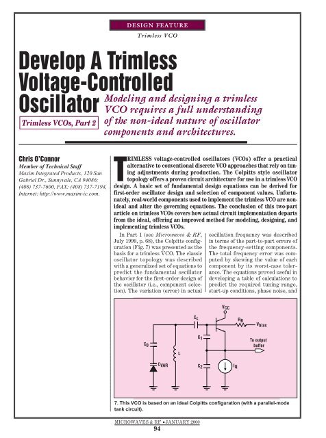
Develop A Trimless Voltage-Controlled Oscillator - Ladyada.net
Develop A Trimless Voltage-Controlled Oscillator - Ladyada.net
Develop A Trimless Voltage-Controlled Oscillator - Ladyada.net

You also want an ePaper? Increase the reach of your titles
YUMPU automatically turns print PDFs into web optimized ePapers that Google loves.
DESIGN FEATURE<br />
<strong>Trimless</strong> VCO<br />
<strong>Develop</strong> A <strong>Trimless</strong><br />
<strong>Voltage</strong>-<strong>Controlled</strong><br />
<strong>Oscillator</strong><br />
<strong>Trimless</strong> VCOs, Part 2<br />
Modeling and designing a trimless<br />
VCO requires a full understanding<br />
of the non-ideal nature of oscillator<br />
components and architectures.<br />
Chris O’Connor<br />
Member of Technical Staff<br />
Maxim Integrated Products, 120 San<br />
Gabriel Dr., Sunnyvale, CA 94086;<br />
(408) 737-7600, FAX: (408) 737-7194,<br />
Inter<strong>net</strong>: http://www.maxim-ic.com.<br />
TRIMLESS voltage-controlled oscillators (VCOs) offer a practical<br />
alternative to conventional discrete VCO approaches that rely on tuning<br />
adjustments during production. The Colpitts style oscillator<br />
topology offers a proven circuit architecture for use in a trimless VCO<br />
design. A basic set of fundamental design equations can be derived for<br />
first-order oscillator design and selection of component values. Unfortunately,<br />
real-world components used to implement the trimless VCO are nonideal<br />
and alter the governing equations. The conclusion of this two-part<br />
article on trimless VCOs covers how actual circuit implementation departs<br />
from the ideal, offering an improved method for modeling, designing, and<br />
implementing trimless VCOs.<br />
In Part 1 (see Microwaves & RF,<br />
July 1999, p. 68), the Colpitts configuration<br />
(Fig. 7) was presented as the<br />
basis for a trimless VCO. The classic<br />
oscillator topology was described<br />
with a generalized set of equations to<br />
predict the fundamental oscillator<br />
behavior for the first-order design of<br />
the oscillator (i.e., component selection).<br />
The variation (error) in actual<br />
oscillation frequency was described<br />
in terms of the part-to-part errors of<br />
the frequency-setting components.<br />
The total frequency error was computed<br />
by skewing the value of each<br />
component by its worst-case tolerance.<br />
The equations proved useful in<br />
developing a table of calculations to<br />
predict the required tuning range,<br />
start-up conditions, phase noise, and<br />
V CC<br />
C c<br />
R B<br />
V bias<br />
C 0<br />
L<br />
C 1<br />
To output<br />
buffer<br />
C VAR<br />
C 2<br />
I Q<br />
7. This VCO is based on an ideal Colpitts configuration (with a parallel-mode<br />
tank circuit).<br />
MICROWAVES & RF ■ JANUARY 2000<br />
94
DESIGN FEATURE<br />
<strong>Trimless</strong> VCO<br />
B<br />
E<br />
B<br />
E<br />
L p<br />
C<br />
+<br />
C pi V g m V 1 1<br />
–<br />
L p<br />
8. This revised small-signal packaged transistor model forms the core of the<br />
new trimless VCO design.<br />
oscillation amplitude. Finally, a firstorder,<br />
step-wise design process was<br />
introduced as a simple approach to<br />
select the initial component values<br />
for the Colpitts configuration with<br />
parallel-mode tank.<br />
Although the basic theory applied<br />
in Part 1 is useful for first-order<br />
design, accurate selection of component<br />
values in a real-world oscillator<br />
requires consideration of important<br />
circuit details. The aim of this article<br />
is to present a possible approach to<br />
more accurately model the realworld<br />
equivalent of the Colpitts oscillator<br />
topology and to apply it to the<br />
trimless VCO concept. The primary<br />
objective is still to provide a simple<br />
design process that permits accurate<br />
selection of the initial component values<br />
close enough so that minimal fine<br />
tuning of the values in the actual circuit<br />
is needed to achieve oscillator<br />
operating requirements. This article<br />
will cover the effects of non-ideal<br />
components and models for them,<br />
layout parasitic elements in a VCO, a<br />
revised oscillator model, a method for<br />
trimless VCO analysis and simulation,<br />
and an example of a Colpitts<br />
oscillator that is constructed from<br />
low-cost, commercial components<br />
and the measured results for tuning<br />
range and phase noise versus predicted<br />
results.<br />
Initial analysis of the basic Colpitts<br />
configuration assumed that each<br />
component was ideal. However,<br />
when a printed-circuit-board (PCB)<br />
solution is implemented with typical<br />
surface-mount components, the real<br />
characteristics for each device must<br />
be taken into account. An examination<br />
of commonly used surface-mount<br />
components quickly reveals that<br />
they are not ideal elements, but that<br />
the elements contain amounts of parasitic<br />
resistance, capacitance, and<br />
inductance. The parasitic elements<br />
alter the frequency response of the<br />
components to the point where the<br />
effective value of the component is<br />
changed at the frequency of interest.<br />
Consequently, the oscillator frequency,<br />
tuning range, and other characteristics<br />
are affected and the real circuit<br />
departs from the operating point<br />
predicted by the first-order analysis<br />
with near-ideal components. The<br />
departure from the ideal needs to be<br />
accounted for in the design phase, in<br />
order to properly select the component<br />
values. A revised model for each<br />
component is required. The following<br />
is an examination of each component<br />
in the oscillator and a proposed circuit<br />
model for each. Again, the<br />
emphasis is on maintaining the simplest<br />
model possible in order to permit<br />
a reasonable analysis and develop<br />
some intuition in design of the<br />
oscillator circuit.<br />
The core of a VCO is typically constructed<br />
from discrete transistors or<br />
an oscillator integrated circuit (IC).<br />
MICROWAVES & RF ■ JANUARY 2000<br />
96<br />
In either case, the device has finite<br />
cutoff (transition) frequency, f T , and<br />
is typically packaged in a plastic<br />
package with metal leads (e.g., SOT-<br />
323). These factors lead to two predominate<br />
non-ideal elements in the<br />
equivalent circuit: capacitance across<br />
the base-emitter leads, and inductance<br />
in series with the base and<br />
emitter (and collector) leads of the<br />
oscillator. The capacitance results<br />
from the inherent junction capacitance<br />
and base-charging capacitance<br />
of the transistor. The full transistor<br />
circuit model would include base<br />
resistance (r b ), collector-base capacitance<br />
(C jc ), finite beta, etc. However,<br />
it is assumed that f T > f OSC , the oscillation<br />
frequency, so that r b and C jccan<br />
be considered negligible along<br />
with the other transistor parasitic<br />
elements and that the input capacitance<br />
is considered to be the dominant<br />
effect.<br />
The inductance is a result of the<br />
parasitic bondwire and lead inductance<br />
of the package and is therefore<br />
modeled as a single lumped inductor.<br />
This lumped inductance can also<br />
include series inductance from the<br />
pin to capacitors C 1 and C 2 . There are<br />
other parasitic elements, such as<br />
additional transistor parasitic elements<br />
and package shunt capacitance<br />
and mutual inductance, but<br />
their effects will be ignored for the<br />
purpose of this discussion. Figure 8<br />
shows a revised model for the transistor<br />
that includes the parasitic<br />
capacitance (C pi ) and inductance<br />
(L p ). Inductance L p is typically 1.5 to<br />
Cathode Anode Cathode R s<br />
L p Anode<br />
9. This revised varactor model is employed in the new trimless VCO design for<br />
tuning purposes.<br />
L<br />
10. This revised inductor model is also part of the new trimless VCO design.<br />
C P<br />
R SV<br />
R SP<br />
L
DESIGN FEATURE<br />
<strong>Trimless</strong> VCO<br />
2.0 nH while capacitance C pi ) is typically<br />
greater than 1 pF. The baseemitter<br />
capacitance is typically<br />
greater than 1 pF for C jc + C b .<br />
The parasitic capacitance, C pi , and<br />
parasitic inductance, L p , have a significant<br />
impact on the frequency<br />
response/input impedance of the<br />
active circuit amplifier. These elements<br />
must be considered and modeled<br />
to properly predict the equivalent<br />
input capacitance and negative<br />
resistance of the Colpitts oscillator<br />
configuration.<br />
With capacitances C 1 and C 2 connected<br />
to the emitter and base leads,<br />
a revised analysis can be performed<br />
to determine the equivalent input<br />
impedance of the active circuit. For <br />
< L p C pi , the inductor on the base side<br />
in series with C pi has only a small<br />
effect on the impedance since the<br />
majority of signal current flows from<br />
the gm stage through the inductor in<br />
the emitter side. Therefore, the circuit<br />
can be simplified to facilitate<br />
analysis by including only the inductor<br />
in the emitter lead on the ideal<br />
model and provide a more intuitive<br />
approximate result. Although the<br />
majority of the signal current flows<br />
through the emitter lead, the capacitance<br />
C pi should be included in the<br />
calculation of the capacitance. A reasonable<br />
approximation is C 1X = C 1 +<br />
C pi . Circuit analysis shows that the<br />
inductance modifies the equivalent<br />
input impedance from the ideal<br />
model case:<br />
CEQ = 1/ ( 1/ C12<br />
) − A/( 1+<br />
A )<br />
× ( gm / ω C1×<br />
C2)<br />
} (16)<br />
2<br />
+ ( gm / w C 1<br />
C 2)<br />
(14) tain the loop gain to 1 + . As a result,<br />
has a reduced affect on modifying the<br />
and<br />
2<br />
− REQ = − R [ 1/( 1+<br />
A )]<br />
(17)<br />
During oscillation, the current<br />
flowing in the oscillator transistor is<br />
varying versus time (typically like a<br />
half-wave rectified sine wave) and<br />
therefore the instantaneous<br />
transconductance, g m , is varying<br />
with time. At equilibrium, the effective<br />
large-signal transconductance,<br />
G m , is lower than the DC bias value of<br />
Zin =− j[( C1<br />
+ C2 ) / wC1C<br />
2]<br />
g m and is only that necessary to sus-<br />
to a revised model case:<br />
input impedance than at its DC bias<br />
point.<br />
Zin<br />
≅− j ( C + C )/ ωC C<br />
One approximation which could be<br />
used for G M is discussed in ref. 5:<br />
{[ 1× 2 1×<br />
2]<br />
2<br />
[ ]<br />
[ ]<br />
− A/( 1 + A )<br />
2<br />
× ( gm / ωC1 × C2) } + 1/( 1+<br />
A )<br />
2<br />
× ( gm / ω C 1 × C 2<br />
)<br />
where A = ωg L<br />
m<br />
p<br />
(15)<br />
The inductor actually makes the<br />
input capacitance appear larger and<br />
the negative resistance appears<br />
smaller. The equivalent capacitance<br />
along with negative resistance may<br />
be expressed by the following equation<br />
as:<br />
Varactor<br />
C p4<br />
C VAR<br />
R SV<br />
Lp<br />
Resonant load<br />
11. The basic Colpitts VCO configuration has been refined to include the<br />
realistic effects of parasitic elements.<br />
{<br />
C 0<br />
C p3<br />
R SL<br />
2<br />
[ ]<br />
GM<br />
≈ n / REQwhere n =<br />
[( CC<br />
+ C12)/ CC]× [( C1×<br />
+ C2)/<br />
C2]<br />
C = C C / ( C + C ) in the... ( )<br />
12 1×<br />
2 1 2 18<br />
The large-signal G m should then be<br />
substituted for g m in the previous<br />
equations.<br />
Detailed simulation of the full circuit<br />
reveals that the expressions<br />
above offer a reasonable estimate of<br />
the actual equivalent input<br />
MICROWAVES & RF ■ JANUARY 2000<br />
98<br />
L<br />
Inductor<br />
C c<br />
C p2<br />
C p1<br />
Active circuit<br />
C 1<br />
C 2<br />
<strong>Oscillator</strong> transistor<br />
C<br />
L p<br />
+<br />
impedance. These approximations<br />
are used later to develop a revised<br />
set of design equations for the<br />
oscillator.<br />
The varactor is essentially a positive-negative<br />
(PN) junction diode<br />
with specially tailored capacitanceversus-voltage<br />
characteristics. As<br />
with all diodes, the device has a finite<br />
static series resistance. It determines<br />
the effective capacitor and<br />
tank Q. The varactor is typically<br />
implemented as a discrete device in a<br />
plastic package (such as a SC-79<br />
package). As with the transistor,<br />
there is a parasitic lead and bondwire<br />
inductance in series with the varactor<br />
device. These two non-ideal<br />
effects—the series inductance and<br />
the series resistance—must be<br />
included to properly predict the oscillation<br />
frequency and the tank Q<br />
(which impacts the phase noise,<br />
startup, and oscillation amplitude) In<br />
particular, the series inductance is a<br />
critical parasitic to model, because it<br />
strongly changes the effective capacitance<br />
of the varactor. (It forms a<br />
series resonant circuit that can occur<br />
very near the desired oscillation frequency.)<br />
Figure 9 shows a revised<br />
model for the varactor which<br />
includes the parasitic resistance and<br />
inductance in series with the with the<br />
anode and cathode leads. The series<br />
inductance is typically 1.5 nH while<br />
the series resistance is typically 0.5<br />
L p<br />
C pi V 1<br />
–<br />
g m V 1
DESIGN FEATURE<br />
<strong>Trimless</strong> VCO<br />
L<br />
to 1.0 .<br />
The primary inductor in the tank<br />
circuit has a self-resonant frequency<br />
that may affect the frequency of<br />
oscillation. A relatively simple model<br />
can be used to describe the inductor<br />
below the self-resonant frequency.<br />
Figure 10 shows the revised model<br />
for the inductor. The series resistance<br />
(R s ) models the loss in the<br />
inductor that sets the Q. Capacitance<br />
(C p ) models the finite self-resonant<br />
frequency. Some manufacturers are<br />
supporting this model for their commercial<br />
devices. 6 However, many<br />
cost-effective surface-mount inductors<br />
that are available today have<br />
sufficiently high self-resonant frequencies<br />
that it is reasonable to consider<br />
the inductor to have negligible<br />
parasitic capacitance. This permits<br />
the inductor to be modeled as purely<br />
an inductance and a series resistance.<br />
The series resistance of the inductance<br />
does need to be modeled to<br />
accurately describe the tank Q.<br />
C<br />
Resonant<br />
load<br />
<br />
12. This model treats an oscillator as an active circuit with a resonant load.<br />
S11<br />
Active<br />
circuit<br />
COUPLING CAPACITORS<br />
The feedback and coupling capacitors<br />
are high-quality RF components.<br />
Typically, the capacitors are<br />
very small (0603, 0402, even 0201)<br />
multilayer ceramic surface-mount<br />
capacitors. That technology’s small<br />
size inherently provides very-high<br />
frequency performance and nearly<br />
ideal frequency characteristics.<br />
Therefore, the capacitors are considered<br />
ideal for the purposes of this<br />
second-order design.<br />
A potentially troublesome nonideal<br />
factor in the PCB level oscillator<br />
design has to do with the parasitic<br />
capacitances and inductances that<br />
are associated with the component<br />
solder pads and interconnect traces.<br />
These parasitic elements must be<br />
extracted from the actual PCB layout<br />
but are typically not available at<br />
the time of design, because the layout<br />
has not been started/completed.<br />
However, it is important to include<br />
them in the oscillator circuit model to<br />
accurately predict the oscillation frequency<br />
and tuning range, so a first<br />
cut layout and analysis of the parasitic<br />
element values are needed. A<br />
choice must be made between modeling<br />
the parasitic elements with transmission<br />
lines or lumped-element<br />
equivalents. Strictly speaking, the<br />
traces/pads are transmission lines,<br />
but the lumped element approach can<br />
provide a more intuitive method of<br />
modeling the parasitic elements and<br />
is valid for compact layouts where<br />
the interconnects are short (< 40 mil)<br />
and wide (>20 mil). In general, if<br />
traces are short then the connection<br />
could be approximated as just a<br />
shunt capacitance to ground. This<br />
permits the simple addition of parasitic<br />
shunt capacitors at the connection<br />
nodes. The parasitic capacitance<br />
at the connection points can be<br />
approximated by a parallel plate<br />
capacitance, C pad , with the plate area<br />
equal to the total pad/trace area.<br />
−15<br />
CPAD = εε r o × ( A/ t) = 13 . × 10<br />
× ( A / t) pF / mil ( for FR4)<br />
(19)<br />
where:<br />
A = the capacitor plate area (in<br />
square mil), and<br />
t = the board thickness (in mil).<br />
The active circuit negative resistance<br />
for the PCB-level oscillator<br />
design is:<br />
2<br />
− RNEQ = − RN[ 1/( 1+<br />
A )]<br />
(20)<br />
where<br />
The resonant load capacitance can<br />
be found from:<br />
A = ωGm LpCVAREQ = CVAR<br />
/( 1 −ω<br />
LC p VAR)<br />
] + Cp4 (21)<br />
CVEQ = ( C0CVAREQ / C0<br />
+ CVAREQ<br />
+ CVAREQ)<br />
+ Cp3 (22)<br />
The resonant frequency or frequency<br />
of oscillation can be found<br />
from:<br />
f o<br />
CTEQ = CVEQ + CIN<br />
( 24)<br />
The quality factor (Q) of the resonant<br />
tank circuit, Q T , can be found<br />
from:<br />
Q = T / 2πL<br />
( 25)<br />
T<br />
RTEQ = RQL || RQC<br />
( 26)<br />
Q<br />
The amplitude of the oscillation<br />
(the RMS voltage) can be found from:<br />
with<br />
R = Q<br />
2<br />
× R Q = 2πLR<br />
QC C SC L SL<br />
2<br />
QL L SL O Q EQ<br />
R = Q × R V = 2I R<br />
× [ J ( β)/ J ( β) ]× V<br />
(28)<br />
1 0<br />
05 .<br />
[ π TEQ ]<br />
~ 1/ 2 ( 23)<br />
TEQ<br />
= 1/ 2πC R ( 27)<br />
C V S<br />
The loop gain can be found from:<br />
where<br />
[ J1( β)/ J0( β) ]≈ 07 . the ratio of the<br />
Bessel functions<br />
Loop gain = g R ( 1 / n)<br />
(29)<br />
m<br />
EQ<br />
peak<br />
where<br />
n ≈ [( CC<br />
+ C12×<br />
)/ Cc]×<br />
( C1X + C2X)/<br />
C2 X (30)<br />
[ ]<br />
The start-up criteria are given by:<br />
[<br />
2<br />
MICROWAVES & RF ■ JANUARY 2000<br />
101
DESIGN FEATURE<br />
<strong>Trimless</strong> VCO<br />
2<br />
m 1 2 EQ T<br />
g / C C >> R / Q<br />
for a min imum 21 : ratio (31)<br />
V CC<br />
The phase noise can be found from:<br />
2 2<br />
n o<br />
2 2 2<br />
o o EQ o<br />
Phase noise = I × ( 1 / V )<br />
[ ]<br />
× ( f / 2Q ) × R /( f − f (32)<br />
where:<br />
f o = the frequency of oscillation,<br />
C VAR = the varactor capacitance,<br />
Q L = the inductor quality factor,<br />
Q T = the tank quality factor,<br />
R EQ = the equivalent tank parallel<br />
resistance,<br />
g m = the oscillator bipolar transistor<br />
transconductance,<br />
V 0 = the RMS tank voltage,<br />
C T = the total tank capacitance,<br />
C 0 = the varactor coupling capacitance,<br />
Q V = the effective varactor quality<br />
factor,<br />
R S = the varactor series resistance,<br />
I Q = the oscillator transistor bias<br />
current, and<br />
I n = the collector shot noise.<br />
One very useful method to view an<br />
oscillator circuit is as a “reflection<br />
amplifier.” This intuitive concept is<br />
described in a classic article by John<br />
Boyles 7 and in a paper by Esdale. 8<br />
The “reflection amplifier” method<br />
permits the engineer to use S-parameters<br />
for design and measurement of<br />
the oscillator. Working with S-<br />
parameters facilitates the modeling<br />
and measurement of the actual oscillator<br />
circuit and helps develop<br />
insight into the circuit’s performance<br />
and potential problems. 9<br />
The “reflection amplifier”<br />
approach basically models the oscillator<br />
as an active circuit with a resonant<br />
load and describes the stable<br />
oscillation point in terms of the relative<br />
impedances. If the active circuit<br />
input S-parameters are plotted as<br />
1/S 11 , then the values can be directly<br />
plotted on a Smith chart with the of<br />
the resonant load. A convenient<br />
aspect of plotting 1/S 11 is that the<br />
impedance of R and X for the active<br />
circuit can be read and multiplied by<br />
–1 to provide the correct values of the<br />
negative resistance and reactance.<br />
This method of plotting the<br />
impedances provides a graphical rep-<br />
B<br />
E<br />
13. This oscillator active circuit is based on the use of a discrete transistor.<br />
resentation of when oscillation conditions<br />
exist.<br />
The basic conditions for oscillation<br />
are:<br />
1. 1/S11 ≤ ,<br />
2. ang(1/S11) = ang(), and<br />
3. the curves of 1/S 11 and must<br />
ultimately intersect each other and<br />
change in opposite angular directions<br />
versus frequency (this occurs at the<br />
peak-oscillator tank amplitude).<br />
The reflection amplifier approach<br />
will be used in the remainder of this<br />
article to model, simulate, and measure<br />
the real oscillator circuit.<br />
The calculations shown are valid as<br />
a method to approximate the initial<br />
values for the components. A spreadsheet<br />
can be developed to compute<br />
the revised component values (available<br />
on request from the author). It is<br />
important to view the circuit’s true<br />
dependency versus frequency, startup<br />
conditions, etc. Computer simulations<br />
should be used to provide a<br />
more rapid, accurate method of modifying<br />
the circuit component values<br />
that govern the oscillation behavior.<br />
Simulation is an efficient way to<br />
make circuit design trade-offs and<br />
adjustments to account for the<br />
changes caused by the non-ideal circuit<br />
elements.<br />
The basic circuit model can be simulated<br />
with a small-signal circuit simulation,<br />
which inherently works in<br />
terms of S-parameters. A “small-signal”<br />
linear circuit simulation is, by<br />
Out<br />
far, the most rapid simulation mode<br />
available. It is best to use a commercial<br />
circuit simulator, such as the<br />
Advanced Design System (ADS)<br />
from Agilent Technologies (Santa<br />
Rosa, CA), MMICAD from Optotek<br />
(Kanata, Ontario, Canada), the Serenade<br />
Suite from Ansoft (Pittsburgh,<br />
PA), and Microwave Office from<br />
Advanced Wave Research (El<br />
Segundo, CA) for this. The simulator<br />
should be set up to use the “reflection<br />
amplifier” method that was previously<br />
mentioned, using the oscillator circuit<br />
model of Fig. 11. The initial values<br />
can be derived from the revised<br />
design equations. Adjustments can<br />
be made to the component values to<br />
return the active circuit and resonant<br />
load impedances back to the values<br />
required for the desired oscillation<br />
frequency, start-up, and tuning<br />
range. In some cases, the values predicted<br />
by the small-signal circuit<br />
model are a sufficient and accurate<br />
estimation of the component values<br />
to proceed directly toward constructing<br />
the actual circuit (Fig. 12). However,<br />
when a more accurate or highly<br />
optimized design is required, it may<br />
be necessary to simulate the actual<br />
active circuit implementation with<br />
detailed models for all devices. The<br />
full oscillator circuit is then simulated<br />
with a time-domain simulator<br />
(e.g., SPICE) or a harmonic-balance<br />
simulator (e.g., Harmonica) to precisely<br />
determine the frequency tun-<br />
MICROWAVES & RF ■ JANUARY 2000<br />
102
DESIGN FEATURE<br />
<strong>Trimless</strong> VCO<br />
ing range and verify that<br />
the circuit design objectives<br />
can be met.<br />
EXAMPLE CIRCUIT<br />
Implementation of the<br />
Colpitts configuration<br />
shown in Fig. 7 is commonly<br />
accomplished with<br />
discrete transistors.<br />
Many options exist for<br />
cost-effective, high f T<br />
transistors packaged in<br />
small plastic packages—<br />
as single and dual<br />
devices. However, in<br />
order to achieve a design<br />
that works down to a<br />
+2.7-VDC supply voltage<br />
with sufficient headroom<br />
for the oscillator device<br />
and output buffer, a<br />
three-transistor circuit is<br />
typically needed. Figure<br />
V CC<br />
10 <br />
C o C<br />
1<br />
c<br />
V TUNE 2 k 6 pF 5 pF<br />
2<br />
C 1<br />
L F 2.7 pF 3<br />
D 1<br />
4.7 nH<br />
C<br />
Alpha<br />
2<br />
4<br />
1.5 pF<br />
SMV1204-34<br />
SHDN<br />
0.1 F<br />
14. Based on a model MAX2620 oscillator IC, this design represents a practical<br />
implementation of the Colpitts oscillator configuration.<br />
Bias<br />
13 shows the possible implementation<br />
of the oscillator active circuitry.<br />
Discrete implementations are<br />
extremely flexible, but possess several<br />
negatives. The primary negatives<br />
of this circuit are significant<br />
variation in biasing versus temperature<br />
and supply voltage, the large<br />
number of components required to<br />
implement the oscillator active circuitry,<br />
and the relatively large PCB<br />
area that is required.<br />
An improved alternative to the<br />
discrete transistor approach is to use<br />
an integrated oscillator IC, such as<br />
the MAX2620 from Maxim Integrated<br />
Products (Sunnyvale, CA), with<br />
an external tank circuit. The<br />
MAX2620 IC integrates the oscillator<br />
transistor, stable biasing, and an<br />
output amplifier in a small uMAX8<br />
package to provide a convenient<br />
method of implementing the oscillator<br />
active circuitry. 10 This approach<br />
permits the designer to focus only on<br />
selecting the external passive component<br />
values, thereby confining the<br />
design task to achieve the required<br />
frequency tuning characteristics.<br />
Figure 14 shows the Colpitts oscillator<br />
configuration using the<br />
MAX2620. The frequency-setting<br />
components are all on the left side of<br />
the circuit. The components that are<br />
connected to the output ports are one<br />
possible option to implement the output<br />
matching to the load.<br />
Referring to the revised circuit<br />
model of Fig. 11, the parasitic-element<br />
values in the component models<br />
are as follows. For the varactor, L p =<br />
1.5 nH, R sv = 0.5 , C var (hi) = 8 pF,<br />
and C var (lo) = 4 pF. For the inductor,<br />
L p = 4.7 nH and R sl = 0.5 . For the<br />
transistor, L p ~ 3.0 nH and Cpi = 1.1<br />
pF. For the layout parasitics, C p1 =<br />
0.2 pF, C p2 = 0.2 pF, C p3 = 0.5 pF, C p4<br />
= 0.3 pF, and L trace = 0.3 nH.<br />
The component values are selected<br />
through a simple design process that<br />
is summarized below as part of the<br />
revised design process:<br />
• Select initial values for C 1 , C 2 , L f ,<br />
C c , C o , C var (hi), and C var (lo) based on<br />
the revised design equations developed<br />
for C var , C v , C in , and C 12e<br />
described in this article to achieve<br />
the require frequency tuning range<br />
required for the trimless VCO.<br />
• Construct a more detailed smallsignal<br />
circuit model using the revised<br />
models for the varactor, active circuit,<br />
and layout parasitic elements.<br />
• Simulate the small-signal circuit<br />
model and adjust the component<br />
value to achieve the target values for<br />
C in , C var(hi) , C var(lo) , and startup conditions<br />
(maintain loop gain and sufficient<br />
negative resistance).<br />
• Construct the oscillator with the<br />
simulated component values.<br />
• Measure 1/S 11 and (optional).<br />
MICROWAVES & RF ■ JANUARY 2000<br />
105<br />
MAX2620<br />
V CC<br />
V CC<br />
10 nH<br />
8<br />
7<br />
6<br />
5<br />
51 <br />
1000 pF<br />
1.5 pF<br />
V CC<br />
0.1 F<br />
330 pF<br />
1000 pF<br />
Out<br />
to<br />
mixer<br />
Out<br />
to PLL<br />
• If any fine-tuning frequency<br />
adjustment is necessary, adjust the<br />
frequency of oscillation with C o , C c<br />
(for an increase in frequency,<br />
decrease C c and for a decrease in frequency,<br />
increase C c ; increase the tuning<br />
range and decrease the frequency<br />
by increasing C o ; and decrease the<br />
tuning until the tuning range and frequency<br />
limits match a particular set<br />
of requirements).<br />
A circuit (Fig. 14) was constructed<br />
in prototype fashion to demonstrate<br />
the performance of an oscillator<br />
designed from the equations and simulation<br />
technique outlined in this<br />
article. The circuit is useful for some<br />
commercial 900-MHz industrial-scientific-medical<br />
(ISM) applications. ••<br />
Acknowledgments<br />
The author would like to acknowledge that there are<br />
many previous contributors to the field of oscillators that<br />
are the respected experts (Rohde, Leeson, Boyles, Hayward,<br />
Meyer, etc.). Their work has led to the advancement<br />
of oscillators in general and provided the foundation for this<br />
two-part article. My effort was simply to introduce a simple<br />
concept for a trimless VCO and to re-describe the oscillator<br />
design task in a simple, improved manner in order to permit<br />
an engineer to quickly calculate the initial component values<br />
for a PCB-based Colpitts VCO design.<br />
References<br />
5. Ken<strong>net</strong>h K. Clarke, Communications Circuits: Analysis<br />
and Design, Addison-Wesley, Boston, 1978, Chap. 6, p.<br />
225.<br />
6. “Modeling Coilcraft RF Inductors,” Technical Note,<br />
Coilcraft, Inc., Lisle, IL, 1999.<br />
7. John W. Boyles, “The <strong>Oscillator</strong> As A Reflection<br />
Amplifier: An Intuitive Approach To <strong>Oscillator</strong> Design,”<br />
Microwave Journal, June 1986.<br />
8. Daniel J. Esdale et al., “A Reflection Coefficient<br />
Approach to the Design of One-Port Negative Impedance<br />
<strong>Oscillator</strong>s,” IEEE Transactions on Microwave Theory<br />
and Techniques, Vol. MTT-29, No. 8, August 1981, pp. 770-<br />
776.<br />
9. “Varactor SPICE Models for RF VCO Applications,”<br />
Application Note, Alpha Industries, Woburn, MA, 1998.<br />
10. Datasheet for the MAX2620, Maxim Integrated Products,<br />
Sunnyvale, CA, 1997.