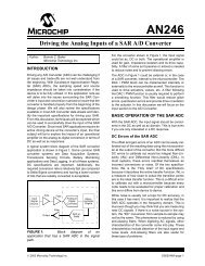
Datasheet
Datasheet
Datasheet

You also want an ePaper? Increase the reach of your titles
YUMPU automatically turns print PDFs into web optimized ePapers that Google loves.
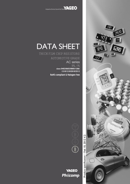
DATA SHEET<br />
THICK FILM CHIP RESISTORS<br />
AUTOMOTIVE GRADE<br />
AC series<br />
5%, 1%<br />
sizes 0402/0603/0805/1206/<br />
1210/1218/2010/2512<br />
RoHS compliant & Halogen free<br />
Product specification – Feb 10, 2012 V.2
Chip Resistor Surface Mount<br />
AC SERIES 0402 to 2512<br />
Product specification 2<br />
10<br />
SCOPE<br />
This specification describes<br />
AC0402 to AC2512 chip resistors<br />
with lead-free terminations made by<br />
thick film process.<br />
APPLICATIONS<br />
•All general purpose applications<br />
•Car electronics, industrial<br />
application<br />
FEATURES<br />
•Comply with AEC-Q200 standard<br />
•Superior resistance against<br />
sulfur containing atmosphere<br />
•MSL class: MSL 1<br />
•AC series soldering is<br />
compliant with J-STD-020D<br />
•Halogen free epoxy<br />
•RoHS compliant<br />
- Products with lead-free<br />
terminations meet RoHS<br />
requirements<br />
- Pb-glass contained in electrodes,<br />
resistor element and glass are<br />
exempted by RoHS<br />
•Reduce environmentally<br />
hazardous waste<br />
•High component and equipment<br />
reliability<br />
•Save PCB space<br />
•The resistors are 100% performed<br />
by automatic optical inspection<br />
prior to taping.<br />
ORDERING INFORMATION - GLOBAL PART NUMBER<br />
Part number is identified by the series name, size, tolerance, packaging<br />
type, temperature coefficient, taping reel and resistance value.<br />
GLOBAL PART NUMBER<br />
AC XXXX X X X XX XXXX L<br />
(1) (2) (3) (4) (5) (6) (7)<br />
(1) SIZE<br />
0402 / 0603 / 0805 / 1206 / 1210 / 1218 / 2010 / 2512<br />
(2) TOLERANCE<br />
F = ±1%<br />
J = ±5% (for Jumper ordering, use code of J)<br />
(3) PACKAGING TYPE<br />
R = Paper/PE taping reel<br />
(4) TEMPERATURE COEFFICIENT OF RESISTANCE<br />
– = Base on spec<br />
(5) TAPING REEL<br />
Resistance rule of global part<br />
number<br />
Resistance coding<br />
Example<br />
rule<br />
XRXX<br />
(1 to 9.76 Ω)<br />
XXRX<br />
(10 to 97.6 Ω)<br />
XXXR<br />
(100 to 976 Ω)<br />
XKXX<br />
(1 to 9.76 KΩ)<br />
XMXX<br />
(1 to 9.76 MΩ)<br />
XXMX<br />
(10 MΩ)<br />
1R = 1 Ω<br />
1R5 = 1.5 Ω<br />
9R76 = 9.76 Ω<br />
10R = 10 Ω<br />
97R6 = 97.6 Ω<br />
100R = 100 Ω<br />
976R = 976 Ω<br />
1K = 1,000 Ω<br />
9K76 = 9760 Ω<br />
1M = 1,000,000 Ω<br />
9M76= 9,760,000 Ω<br />
10M = 10,000,000 Ω<br />
K = Embossed taping reel<br />
07 = 7 inch dia. Reel 10 = 10 inch dia. Reel<br />
13 = 13 inch dia. Reel 7D = 7 inch dia. Reel with double quantity<br />
(6) RESISTANCE VALUE<br />
1Ω to 10 MΩ<br />
There are 2~4 digits indicated the resistance value. Letter R/K/M is decimal point, no<br />
need to mention the last zero after R/K/M, e.g.1K2, not 1K20.<br />
Detailed coding rules of resistance are shown in the table of “Resistance rule of<br />
global part number”.<br />
(7) DEFAULT CODE<br />
Letter L is the system default code for ordering only. (Note)<br />
ORDERING EXAMPLE<br />
The ordering code for an AC0402<br />
chip resistor, value 100 KX with<br />
±1% tolerance, supplied in 7-inch<br />
tape reel is: AC0402FR-07100KL.<br />
NOTE<br />
1. All our RSMD products are RoHS<br />
compliant and Halogen free. "LFP" of the<br />
internal 2D reel label states "Lead-Free<br />
Process".<br />
2. On customized label, "LFP" or specific<br />
symbol can be printed.<br />
3. AC series with ±0.5% tolerance is also<br />
available. For further information, please<br />
contact sales.<br />
Feb 10, 2012 V.2<br />
www.yageo.com
ynsc007<br />
YNSC001<br />
YNSC<br />
YNSC004<br />
Chip Resistor Surface Mount<br />
AC SERIES 0402 to 2512<br />
Product specification 3<br />
10<br />
MARKING<br />
AC0402<br />
No marking<br />
Fig. 1<br />
AC0603 / AC0805 / AC1206 / AC1210 / AC2010 / AC2512<br />
Fig. 2<br />
03<br />
Value=10 KΩ<br />
E-24 series: 3 digits, ±5%<br />
First two digits for significant figure and 3rd digit for number of zeros<br />
AC0603<br />
Fig. 3<br />
0<br />
Value = 24 Ω<br />
E-24 series: 3 digits, ±1%<br />
One short bar under marking letter<br />
Fig. 4<br />
Value = 12.4 KΩ<br />
E-96 series: 3 digits, ±1%<br />
First two digits for E-96 marking rule and 3rd letter for number of zeros<br />
AC0805 / AC1206 / AC1210 / AC2010 / AC2512<br />
00<br />
Fig. 5 Value = 10 KΩ<br />
Both E-24 and E-96 series: 4 digits, ±1%<br />
First three digits for significant figure and 4th digit for number of zeros<br />
AC1218<br />
YNSC099<br />
Fig. 6 Value = 10 KΩ<br />
E-24 series: 3 digits, ±5%<br />
First two digits for significant figure and 3rd digit for number of zeros<br />
00<br />
YNSC103<br />
Fig. 7 Value = 10 KΩ<br />
Both E-24 and E-96 series: 4 digits, ±1%<br />
First three digits for significant figure and 4th digit for number of zeros<br />
NOTE<br />
For further marking information, please refer to data sheet “Chip resistors marking”. Marking of AC series is the same as RC series.<br />
Feb 10, 2012 V.2<br />
www.yageo.com
Chip Resistor Surface Mount<br />
AC SERIES 0402 to 2512<br />
Product specification 4<br />
10<br />
CONSTRUCTION<br />
The resistors are constructed on top of an automotive<br />
grade ceramic body. Internal metal electrodes are<br />
added at each end and connected by a resistive glaze.<br />
The resistive glaze is covered by a lead-free glass.<br />
The composition of the glaze is adjusted to give the<br />
approximately required resistance value and laser<br />
trimming of this resistive glaze achieves the value within<br />
tolerance. The whole element is covered by a protective<br />
overcoat. Size 0603 and bigger is marked with the<br />
resistance value on top. Finally, the two external<br />
terminations (Ni / matte tin) are added, as shown in Fig.8.<br />
OUTLINES<br />
YNSC088<br />
marking layer<br />
overcoat<br />
protective glass<br />
resistive layer<br />
(Jumper chip is a conductor)<br />
inner electrode<br />
termination(Ni/matte tin)<br />
inner electrode<br />
ceramic substrate<br />
Fig. 8 Chip resistor outlines<br />
DIMENSIONS<br />
Table 1 For outlines, please refer to Fig. 9<br />
TYPE L (mm) W (mm) H (mm) I1 (mm) I2 (mm)<br />
AC0402 1.00 ±0.05 0.50 ±0.05 0.32 ±0.05 0.20 ±0.10 0.25 ±0.10<br />
AC0603 1.60 ±0.10 0.80 ±0.10 0.45 ±0.10 0.25 ±0.15 0.25 ±0.15<br />
AC0805 2.00 ±0.10 1.25 ±0.10 0.50 ±0.10 0.35 ±0.20 0.35 ±0.20<br />
AC1206 3.10 ±0.10 1.60 ±0.10 0.55 ±0.10 0.45 ±0.20 0.40 ±0.20<br />
AC1210 3.10 ±0.10 2.60 ±0.15 0.50 ±0.10 0.45 ±0.15 0.50 ±0.20<br />
AC1218 3.10 ±0.10 4.60 ±0.10 0.55 ±0.10 0.45 ±0.20 0.40 ±0.20<br />
AC2010 5.00 ±0.10 2.50 ±0.15 0.55 ±0.10 0.55 ±0.15 0.50 ±0.20<br />
AC2512 6.35 ±0.10 3.10 ±0.15 0.55 ±0.10 0.60 ±0.20 0.50 ±0.20<br />
For dimension, please refer to Table 1<br />
AC0402/0603/0805/1206/<br />
1210/2010/2512<br />
AC1218<br />
I 1<br />
Side view for all type<br />
I 1<br />
W<br />
I 2<br />
W<br />
H<br />
Fig. 9 Chip resistor dimensions<br />
L<br />
L<br />
YNSC096<br />
www.yageo.com<br />
Feb 10, 2012 V.2
Chip Resistor Surface Mount<br />
AC SERIES 0402 to 2512<br />
Product specification 5<br />
10<br />
ELECTRICAL CHARACTERISTICS<br />
Table 2<br />
CHARACTERISTICS<br />
TYPE<br />
RESISTANCE<br />
RANGE<br />
Operating<br />
Temperature<br />
Range<br />
Max.<br />
Working<br />
Voltage<br />
Max.<br />
Overload<br />
Voltage<br />
Dielectric<br />
Withstanding<br />
Voltage<br />
Temperature<br />
Coefficient<br />
of Resistance<br />
Jumper Criteria<br />
AC0402 50 V 100 V 100 V<br />
AC0603 50 V 100 V 100 V<br />
AC0805 150 V 300 V 300 V<br />
AC1206 5% (E24), 1% (E24/E96)<br />
200 V 400 V 500 V<br />
1 Ω to 10 MΩ –55 °C to +155 °C<br />
AC1210 Jumper < 0.05 Ω<br />
200 V 500 V 500 V<br />
AC1218 200 V 500 V 500 V<br />
AC2010 200 V 500 V 500 V<br />
AC2512<br />
200 V 500 V 500 V<br />
1 Ω ≤ R ≤ 10 Ω ,<br />
±200 ppm/°C<br />
10 Ω < R ≤ 10 MΩ ,<br />
±100 ppm/°C<br />
Rated Current 1A<br />
Max. Current 2A<br />
Rated Current 1A<br />
Max. Current 2A<br />
Rated Current 2A<br />
Max. Current 5A<br />
Rated Current 2A<br />
Max. Current 10A<br />
Rated Current 2A<br />
Max. Current 10A<br />
Rated Current 6A<br />
Max. Current 10A<br />
Rated Current 2A<br />
Max. Current 10A<br />
Rated Current 2A<br />
Max. Current 10A<br />
FOOTPRINT AND SOLDERING PROFILES<br />
Recommended footprint and soldering profiles of AC-series is the same as RC-series. Please refer to data sheet<br />
“Chip resistors mounting”.<br />
PACKING STYLE AND PACKAGING QUANTITY<br />
Table 3 Packing style and packaging quantity<br />
PACKING STYLE<br />
REEL<br />
DIMENSION<br />
Paper/PE taping reel (R) 7" (178 mm) 10,000<br />
20,000<br />
AC0402 AC0603 AC0805 AC1206 AC1210 AC1218 AC2010 AC2512<br />
5,000 5,000 5,000 5,000 --- --- ---<br />
10" (254 mm) 20,000 10,000 10,000 10,000 --- --- --- ---<br />
13" (330 mm) 50,000 20,000 20,000 20,000 20,000 --- --- ---<br />
Embossed taping reel (K) 7" (178 mm) --- --- --- --- --- 4,000 4,000 4,000<br />
NOTE<br />
1. For paper/PE/embossed tape and reel specifications/dimensions, please refer to data sheet “Chip resistors packing”.<br />
Feb 10, 2012 V.2<br />
www.yageo.com
Chip Resistor Surface Mount<br />
AC SERIES 0402 to 2512<br />
Product specification 6<br />
10<br />
FUNCTIONAL DESCRIPTION<br />
OPERATING TEMPERATURE RANGE<br />
Range: –55 °C to +155 °C<br />
POWER RATING<br />
Each type rated power at 70 °C:<br />
AC0402=1/16 W (0.0625W)<br />
AC0603=1/10 W (0.1W)<br />
AC0805=1/8 W (0.125W)<br />
AC1206=1/4 W (0.25W)<br />
AC1210=1/2 W (0.5W)<br />
AC1218=1 W<br />
AC2010=3/4 W (0.75W)<br />
AC2512=1 W<br />
RATED VOLTAGE<br />
The DC or AC (rms) continuous working voltage<br />
corresponding to the rated power is determined by<br />
the following formula:<br />
V = √(P X R)<br />
Or Maximum working voltage whichever is less<br />
handbook, halfpage<br />
P<br />
(%P rated)<br />
100<br />
50<br />
0<br />
55 0<br />
50<br />
70 100<br />
MLB206_2<br />
155<br />
o<br />
T amb ( C)<br />
Fig. 10 Maximum dissipation (P max ) in percentage of rated power<br />
as a function of the operating ambient temperature (T amb )<br />
Where<br />
V = Continuous rated DC or AC (rms) working voltage (V)<br />
P = Rated power (W)<br />
R = Resistance value (X)<br />
Feb 10, 2012 V.2<br />
www.yageo.com
Chip Resistor Surface Mount<br />
AC SERIES 0402 to 2512<br />
Product specification 7<br />
10<br />
TESTS AND REQUIREMENTS<br />
Table 4 Test condition, procedure and requirements<br />
TEST TEST METHOD PROCEDURE REQUIREMENTS<br />
High Temperature AEC-Q200 Test 3<br />
1,000 hours at TA = 125 °C, unpowered ±(1.0%+0.05 Ω)<br />
Exposure<br />
MIL-STD-202 Method 108<br />
Chip Resistor Surface Mount<br />
AC SERIES 0402 to 2512<br />
Product specification 8<br />
10<br />
TEST TEST METHOD PROCEDURE REQUIREMENTS<br />
Solderability<br />
- Wetting AEC-Q200 Test 18<br />
J-STD-002<br />
Electrical Test not required Magnification 50X<br />
SMD conditions:<br />
(a) Method B, aging 4 hours at 155 °C dry heat,<br />
dipping at 235±3 °C for 5±0.5 seconds.<br />
(b) Method B, steam aging 8 hours, dipping at<br />
215±3 °C for 5±0.5 seconds.<br />
(c) Method D, steam aging 8 hours, dipping at<br />
260±3 °C for 7±0.5 seconds.<br />
Well tinned (≥95% covered)<br />
No visible damage<br />
Board Flex AEC-Q200 Test 21<br />
AEC-Q200-005<br />
Chips mounted on a 90mm glass epoxy resin<br />
PCB (FR4)<br />
Bending for 0402: 5 mm<br />
0603/0805: 3 mm<br />
1206 and above: 2 mm<br />
Holding time: minimum 60 seconds<br />
±(1.0%+0.05 Ω)<br />
Chip Resistor Surface Mount<br />
AC SERIES 0402 to 2512<br />
Product specification 9<br />
10<br />
REVISION HISTORY<br />
REVISION DATE CHANGE NOTIFICATION DESCRIPTION<br />
Version 2 Feb. 10, 2012 - Jumper criteria added<br />
- AC1218 marking and outline figure updated<br />
Version 1 Feb. 01, 2011 - - Case size 1210, 1218, 2010, 2512 extended<br />
- Test method and procedure updated<br />
- Packing style of 7D added<br />
Version 0 Nov. 10, 2010 - - First issue of this specification<br />
Feb 10, 2012 V.2<br />
www.yageo.com
Chip Resistor Surface Mount<br />
AC SERIES 0402 to 2512<br />
Product specification 10<br />
10<br />
LEGAL DISCLAIMER<br />
Yageo, its distributors and agents (collectively, “Yageo”), hereby disclaims any and all liabilities for any errors,<br />
inaccuracies or incompleteness contained in any product related information, including but not limited to<br />
product specifications, datasheets, pictures and/or graphics. Yageo may make changes, modifications and/or<br />
improvements to product related information at any time and without notice.<br />
Yageo makes no representation, warranty, and/or guarantee about the fitness of its products for any particular<br />
purpose or the continuing production of any of its products. To the maximum extent permitted by law, Yageo<br />
disclaims (i) any and all liability arising out of the application or use of any Yageo product, (ii) any and all<br />
liability, including without limitation special, consequential or incidental damages, and (iii) any and all implied<br />
warranties, including warranties of fitness for a particular purpose, non-infringement and merchantability.<br />
Yageo statements regarding the suitability of products for certain types of applications are based on Yageo’s<br />
knowledge of typical operating conditions for such types of applications in a generic nature. Such statements<br />
are neither binding statements of Yageo nor intended to constitute any warranty concerning the suitability for a<br />
specific customer application or use. They are intended for use only by customers with requisite knowledge and<br />
experience for determining whether Yageo products are the correct products for their application or use. In<br />
addition, unpredicatable and isolated cases of product failure may still occur, therefore, customer application or<br />
use of Yageo products which requires higher degree of reliability or safety, shall employ additional protective<br />
safeguard measures to ensure that product failure would not result in personal injury or property damage.<br />
Yageo products are not designed for application or use in medical, life-saving, or life-sustaining devices or for<br />
any other application or use in which the failure of Yageo products could result in personal injury or death.<br />
Customers using or selling Yageo products not expressly indicated for above-mentioned purposes shall do so at<br />
their own risk and agree to fully indemnify Yageo and hold Yageo harmless.<br />
Information provided here is intended to indicate product specifications only. Yageo reserves all the rights for<br />
revising this content without further notification, as long as products are unchanged. Any product change will<br />
be announced by PCN.<br />
Feb 10, 2012 V.2<br />
www.yageo.com