Circuits on Cellulose - University of Cincinnati
Circuits on Cellulose - University of Cincinnati
Circuits on Cellulose - University of Cincinnati

Create successful ePaper yourself
Turn your PDF publications into a flip-book with our unique Google optimized e-Paper software.
48 | FEB 2013 | North American | SPECTRUM.IEEE.ORG
C i r c u i ts o n C e l lu l o s e<br />
Pa p e r e l ect r o n i c s c o u l d pav e t h e way to a<br />
n e w g e n e r at i o n o f c h e a p, f l e x i b l e g a d g e ts<br />
By A n d r e w J . S t e c k l<br />
You wake up with a heavy head. Was it the half dozen glasses <strong>of</strong> champagne last<br />
night or are you getting sick? In your bathroom is a little strip <strong>of</strong> paper that can tell<br />
you for sure. You place it <strong>on</strong> your t<strong>on</strong>gue and after a few sec<strong>on</strong>ds, you pull it back to<br />
see the bad news: There’s a small green dot next to the word “flu.” When you fish your<br />
doctor’s business card out <strong>of</strong> your wallet, you notice it looks different from the last<br />
time you looked at it. The ph<strong>on</strong>e number for his <strong>of</strong>fice was originally black. Now it’s<br />
displayed in blinking red letters, a sign that the number was changed recently.<br />
The electr<strong>on</strong>ics in this scenario are not far <strong>of</strong>f; in fact the basic technological breakthroughs<br />
needed to make them work have all been achieved in the past few years. At<br />
the moment the costs are still too high for them to be used in things like business cards<br />
or package labels, but remarkable advances in materials science and simpler fabricati<strong>on</strong><br />
methods are setting the stage for a whole new breed <strong>of</strong> cheap, bendable, disposable,<br />
and perhaps even recyclable electr<strong>on</strong>ics. And some <strong>of</strong> the most exciting work in<br />
this field is happening with paper.<br />
At first glance, paper might seem like an unlikely fr<strong>on</strong>t-runner in the flexible electr<strong>on</strong>ics<br />
race. Straight <strong>of</strong>f the shelf, the material isn’t nearly as rugged as plastic or as smooth<br />
SPECTRUM.IEEE.ORG | North American | FEB 2013 | 49
as new, bendable forms <strong>of</strong> glass. And at a<br />
microscopic level it’s just a tangle <strong>of</strong> cellulose<br />
fibers, hardly the sort <strong>of</strong> structure<br />
that’s ideal for making a bunch <strong>of</strong> finely<br />
featured, identical circuit comp<strong>on</strong>ents.<br />
But paper actually has a lot going for it.<br />
It’s lightweight, flexible, biodegradable,<br />
and it comes from a renewable resource.<br />
It’s also extraordinarily adaptable: With<br />
the right set <strong>of</strong> additives and manufacturing<br />
processes, paper can take <strong>on</strong> a seemingly<br />
endless range <strong>of</strong> properties. It can be<br />
made hydrophilic or hydrophobic, porous<br />
or watertight, opaque or nearly transparent,<br />
delicate or str<strong>on</strong>g, coarse or about as<br />
smooth as glass.<br />
Paper electr<strong>on</strong>ics also have the potential<br />
to be extraordinarily cheap. The material<br />
itself is intrinsically inexpensive;<br />
c<strong>on</strong>venti<strong>on</strong>al varieties cost about a tenth<br />
as much as plastic film. Even the special<br />
paper that’s tailor-made for electr<strong>on</strong>ics<br />
costs, area for area, about 1 percent as<br />
much as silic<strong>on</strong>. Roll-to-roll presses can<br />
print microscopic features <strong>on</strong> wide reams<br />
at speeds <strong>of</strong> up to 30 meters per sec<strong>on</strong>d—<br />
about three times as fast as the Olympian<br />
Usain Bolt can run.<br />
When my research group at the <strong>University</strong><br />
<strong>of</strong> <strong>Cincinnati</strong> first started working with<br />
paper in 2008, we weren’t thinking too<br />
broadly about the material’s potential as<br />
the base layer, or substrate, for electr<strong>on</strong>ics.<br />
We were originally interested in a relatively<br />
narrow applicati<strong>on</strong>, what might be called<br />
“e-paper <strong>on</strong> paper,” essentially electr<strong>on</strong>ic<br />
displays built directly <strong>on</strong> paper. The initial<br />
pro<strong>of</strong>-<strong>of</strong>-principle experiment worked<br />
far better than we expected, and in the<br />
years since, I’ve become c<strong>on</strong>vinced that<br />
paper’s potential could be just as broad<br />
(if not as deep) as silic<strong>on</strong>’s has turned out<br />
to be. Paper has already shown promise as<br />
a substrate for sensors, biological assays,<br />
RF antennas, batteries, circuit boards, and<br />
smart packaging labels. In the next few<br />
years, we’ll start to see the first gadgets<br />
based <strong>on</strong> this technology make their way<br />
out <strong>of</strong> the laboratory and into the hands<br />
<strong>of</strong> c<strong>on</strong>sumers and business users.<br />
Tra n s i sto rs<br />
Source<br />
Channel<br />
Paper substrate<br />
flexible stack: Transistors <strong>on</strong> flexible substrates can be built using organic or inorganic<br />
semic<strong>on</strong>ducting channels. This schematic illustrates a way <strong>of</strong> making an organic switch.<br />
in a tech world dominated by plastic, glass, and silic<strong>on</strong>, it may come as a<br />
surprise to learn that research into paper electr<strong>on</strong>ics actually dates back nearly<br />
50 years. In the late 1960s, Peter Brody’s group at Westinghouse Electric Corp.<br />
experimented with paper, am<strong>on</strong>g other materials, as a substrate for thin-film transistors,<br />
the sort that could be built into switching arrays to c<strong>on</strong>trol individual pixels<br />
in a liquid-crystal display.<br />
Even then, before a wealth <strong>of</strong> coating and processing innovati<strong>on</strong>s came <strong>on</strong> the<br />
scene, paper had a number <strong>of</strong> attractive attributes. Chief am<strong>on</strong>g those was its quality<br />
as an electrical insulator. Paper generally boasts a resistivity <strong>of</strong> some 10 billi<strong>on</strong><br />
ohm-centimeters, about 100 000 times the intrinsic resistivity <strong>of</strong> silic<strong>on</strong>. That means<br />
the material should, in theory, work quite well as a substrate for electr<strong>on</strong>ic devices.<br />
It resists the flow <strong>of</strong> current so well that it effectively eliminates <strong>on</strong>e <strong>of</strong> the most comm<strong>on</strong><br />
pathways electr<strong>on</strong>s use to sneak across a transistor when it’s supposed to be <strong>of</strong>f.<br />
That isn’t to say paper is the ideal material <strong>on</strong> which to build transistors. Materials<br />
like glass and traditi<strong>on</strong>al semic<strong>on</strong>ductors are easy to manufacture with variati<strong>on</strong>s in<br />
surface height <strong>of</strong> a few nanometers or less. But height variati<strong>on</strong>s in paper range from<br />
at best a fracti<strong>on</strong> <strong>of</strong> a micrometer up to several micrometers, depending <strong>on</strong> the fiber<br />
size and how well those fibers commingle to form a flat mat. Electr<strong>on</strong>ic devices built<br />
<strong>on</strong> such an irregular surface are likely to vary greatly in performance, and a sizable<br />
proporti<strong>on</strong> will not work at all.<br />
Despite that, about five years ago, as interest in electr<strong>on</strong>ic readers and flexible reflective<br />
displays took <strong>of</strong>f, researchers began to explore paper as an electr<strong>on</strong>ics substrate.<br />
The potential pay<strong>of</strong>f was big: If they could build the back-end circuitry needed to c<strong>on</strong>trol<br />
pixels, they’d be halfway to creating a changeable reflective display that naturally has<br />
the look and feel <strong>of</strong> paper (and is just as thin, lightweight, and flexible).<br />
Drain<br />
Gate<br />
Dielectric<br />
Since then, about a half-dozen research groups have made c<strong>on</strong>siderable headway in<br />
c<strong>on</strong>structing paper-based transistors. They’ve used either inorganic semi c<strong>on</strong>ductors<br />
like silic<strong>on</strong> or indium gallium zinc oxide for the current-carrying channels or organic<br />
materials like pentacene or P3HT. A good part <strong>of</strong> this progress has followed from finding<br />
Previous Pages: Adam Zocco/Andrew J. Steckl/<strong>University</strong> <strong>of</strong> <strong>Cincinnati</strong><br />
Illustrati<strong>on</strong> by Emily Cooper
Top: Duk-Young Kim/Andrew J. Steckl/<strong>University</strong> <strong>of</strong> <strong>Cincinnati</strong>; Bottom: Jin-Young Kim/sungkyungkwan university<br />
or developing the right kinds <strong>of</strong> paper. The best<br />
are those that have special polymer coatings<br />
that help fill in troughs in the surface and seal<br />
the paper to prevent chemical degradati<strong>on</strong> during<br />
the fabricati<strong>on</strong> process.<br />
Paper would simply combust at the temperatures<br />
used to grow and treat the crystalline films<br />
used in traditi<strong>on</strong>al semic<strong>on</strong>ductors, so inorganic<br />
paper-based transistors are typically made from<br />
amorphous, n<strong>on</strong>crystalline films. These can be<br />
formed at a lower temperature using the standard<br />
techniques <strong>of</strong> depositing a material in a<br />
vacuum, such as evaporati<strong>on</strong> or sputtering. This<br />
fabricati<strong>on</strong> strategy is straightforward, but the<br />
resulting transistors tend to embrace paper’s<br />
inherent textural variati<strong>on</strong>, the result being that<br />
the voltage needed to get current to flow in them<br />
can be a dozen times as much as what’s needed<br />
to move electr<strong>on</strong>s through transistors built <strong>on</strong><br />
glass or silic<strong>on</strong>. John Rogers’s group at the<br />
<strong>University</strong> <strong>of</strong> Illinois at Urbana-Champaign, for<br />
example, has been perfecting an alternative approach<br />
in which circuits are built <strong>on</strong> silic<strong>on</strong> and<br />
then transferred to paper (or other substrates)<br />
<strong>on</strong>ce they’re finished. This method tends to create<br />
better-performing circuits, although the fabricati<strong>on</strong><br />
process is c<strong>on</strong>siderably more involved,<br />
and it’s also more costly, because it would start<br />
with a silic<strong>on</strong> wafer.<br />
When it comes to mass producti<strong>on</strong>, however,<br />
the organic semic<strong>on</strong>ductors may be the way to<br />
go. Unlike inorganic materials, organic compounds<br />
can be dissolved in fluid and deposited<br />
<strong>on</strong> paper using roll-to-roll printers, just as with<br />
ordinary ink. But this approach still faces some<br />
obstacles. For <strong>on</strong>e, the transistors tend to be<br />
slower, due to the intrinsic properties <strong>of</strong> organic<br />
semic<strong>on</strong>ductors. And organic switches are naturally<br />
more sensitive to envir<strong>on</strong>mental c<strong>on</strong>diti<strong>on</strong>s.<br />
Oxygen and water vapor, for example,<br />
can degrade or even open up a gap between<br />
an organic material and a metal electrode<br />
through chemical degradati<strong>on</strong> by oxidati<strong>on</strong> or<br />
by partially dissolving the structure. Surface<br />
treatments can help make paper—which naturally<br />
sops up moisture from the air that could<br />
affect the device built <strong>on</strong> top— relatively impermeable.<br />
But a fix is still needed to ensure that<br />
organic circuits perform well over l<strong>on</strong>g periods<br />
in relatively humid envir<strong>on</strong>ments.<br />
P i xe l s<br />
Thin-film circuits built <strong>on</strong> paper are too slow to be c<strong>on</strong>sidered for general<br />
purpose computing, but they are an attractive means for c<strong>on</strong>trolling and interacting<br />
with “outward-facing” devices such as sensors, displays, and energy-harvesting gear.<br />
Building such devices <strong>on</strong> paper can be just as challenging as building back-end electr<strong>on</strong>ics.<br />
But there has been a lot <strong>of</strong> progress, particularly in the relatively inexpensive and<br />
low-power realm <strong>of</strong> reflective displays. One promising approach is the electrochromic<br />
display, which uses pixels made <strong>of</strong> a c<strong>on</strong>ducting polymer. If a sufficient voltage is applied<br />
to such a pixel, electr<strong>on</strong>s will be knocked <strong>of</strong>f and the optical properties <strong>of</strong> the polymer will<br />
change, turning it from, say, dark blue to transparent. This approach, which was pi<strong>on</strong>eered<br />
by Magnus Berggren’s group at Linköping <strong>University</strong>, in Sweden, has many advantages.<br />
For <strong>on</strong>e, it requires just a few volts to operate, and it’s structurally fairly simple. But there<br />
are a few drawbacks. The color palette is limited, and the switching speed is quite slow.<br />
It can take anywhere from a fracti<strong>on</strong> <strong>of</strong> a sec<strong>on</strong>d to several sec<strong>on</strong>ds to complete pixel<br />
transformati<strong>on</strong>, which makes the display unsuitable for full-moti<strong>on</strong> video.<br />
At the <strong>University</strong> <strong>of</strong> <strong>Cincinnati</strong>, my group has been working <strong>on</strong> adapting an alternative<br />
display approach called electrowetting, which is traditi<strong>on</strong>ally used with glass. Electrowetting<br />
works by c<strong>on</strong>fining liquids between two surfaces and then altering their surface<br />
tensi<strong>on</strong>, using an applied voltage. Altering the surface tensi<strong>on</strong> causes the colored liquid<br />
to either spread out and reflect light or<br />
ball up and allow the light through. Paper<br />
hardly seems a natural fit for this technique.<br />
Electrowetting displays typically<br />
use liquids like water and oil that are<br />
readily absorbed by paper. Pixels also<br />
need to be built <strong>on</strong> a very smooth, glasslike<br />
surface to ensure reliability and fast<br />
resp<strong>on</strong>se. With a rough surface, it’s very<br />
hard to guarantee that liquids will move<br />
where they’re supposed to every time.<br />
We first tried the same sort <strong>of</strong> waxcoated<br />
papers that you might find in your<br />
kitchen cupboard, standard “smoothfinish”<br />
commercial papers, and also<br />
a translucent paper called glassine.<br />
Although the surfaces <strong>of</strong> all these paper<br />
<strong>on</strong> display: Paper can be used<br />
to make displays that either reflect<br />
incoming light or emit their own.<br />
One way to make a reflective display<br />
is to alter the surface tensi<strong>on</strong> <strong>of</strong> liquid<br />
pixels [top]. Organic light-emitting<br />
diodes can also be built <strong>on</strong> paper to<br />
make displays that glow [bottom].<br />
SPECTRUM.IEEE.ORG | North American | FEB 2013 | 51
types resist water, they eventually did<br />
absorb the liquid. Then we were c<strong>on</strong>tacted<br />
by the Bost<strong>on</strong>-based Sappi<br />
Fine Paper North America, which<br />
had created a polymer-coated paper<br />
with an average surface roughness<br />
<strong>of</strong> a couple <strong>of</strong> nanometers, just<br />
a little higher than that <strong>of</strong> glass. That<br />
seemed to be just the thing. With that<br />
material, we were able to make reliable<br />
pixels with switching times as short as<br />
10 millisec<strong>on</strong>ds—nearly suitable for<br />
video. We are now working to develop<br />
paper-based displays using electrowetting.<br />
We think this approach might<br />
be ideal for smart labels <strong>on</strong> packages<br />
that could, for example, show videos<br />
about how the product is to be used, or<br />
for displays—c<strong>on</strong>taining vital informati<strong>on</strong><br />
for soldiers in the field—that can be<br />
rapidly destroyed if necessary.<br />
For both displays and back-end<br />
electr<strong>on</strong>ics, fabricati<strong>on</strong> still remains<br />
a problem. The fastest, cheapest way to build<br />
paper electr<strong>on</strong>ics is to use a roll-to-roll printer.<br />
But the state-<strong>of</strong>-the-art resoluti<strong>on</strong> <strong>of</strong> these machines<br />
is currently about 10 micrometers. So flexible<br />
electr<strong>on</strong>ics fabricated with these machines<br />
would have feature sizes about the same as those<br />
<strong>of</strong> silic<strong>on</strong>-based chips in 1971, when microprocessors<br />
had about 2000 transistors. Improving<br />
this resoluti<strong>on</strong> without sacrificing printing<br />
speed will take years and significant investment.<br />
That being said, size isn’t everything. Displays—<br />
particularly if they can be c<strong>on</strong>structed ec<strong>on</strong>omically—can<br />
still be quite readable and attractive<br />
even if they’re c<strong>on</strong>structed from comp<strong>on</strong>ents that<br />
are much larger than those needed for advanced<br />
integrated circuits. (After all, today’s state-<strong>of</strong>the-art<br />
tablets and e-readers boast pixel sizes<br />
<strong>of</strong> about 100 µm, which is about 10 000 times<br />
as large as the minimum feature sizes needed<br />
to build state-<strong>of</strong>-the-art memory chips.) Some<br />
circuit comp<strong>on</strong>ents need larger features to<br />
functi<strong>on</strong> well. Radio-frequency ID tags, for example,<br />
need relatively large antennas to be able<br />
to pick up and transmit electromag netic waves<br />
with radio wavelengths. Even the smallest RFID<br />
chips reported to date are about 50 µm <strong>on</strong> a side.<br />
And high-voltage power electr<strong>on</strong>ics tend to perform<br />
better when they’re made bigger, because<br />
spreading a load over a large area reduces the<br />
chance <strong>of</strong> electrical breakdown. This is a realm<br />
where paper has already been used for many<br />
years, as an insulator in transformers.<br />
M i c r <strong>of</strong> l u i d i c s<br />
Those <strong>of</strong> us building paper-based electr<strong>on</strong>ic devices and displays are, to a certain<br />
extent, working against paper’s intrinsic properties. But there is <strong>on</strong>e potential<br />
applicati<strong>on</strong> area where paper is clearly a natural fit: micr<strong>of</strong>luidics.<br />
Micr<strong>of</strong>luidic devices work by transporting liquids<br />
from <strong>on</strong>e spot to another. In the realm <strong>of</strong> biomedical<br />
Post your comments<br />
technology, they’re particularly useful because they<br />
<strong>on</strong>line at http://spectrum. allow you to perform tests like DNA analysis or toxin<br />
ieee.org/paper0213<br />
detecti<strong>on</strong> <strong>on</strong> small liquid volumes, which cuts down <strong>on</strong><br />
costly chemicals and reagents and greatly reduces the<br />
amount <strong>of</strong> bodily fluids that must be extracted from patients. To date, most micr<strong>of</strong>luidic<br />
units have been high-precisi<strong>on</strong> affairs that rely <strong>on</strong> plastic feed tubes and<br />
externally powered pumps, which can take up a fair amount <strong>of</strong> counter space. If patterned<br />
correctly, paper could be used to perform similar tests without these external<br />
accessories. The narrow channels between fibers in paper excel at drawing in water<br />
and other fluids automatically by capillary acti<strong>on</strong>.<br />
Some companies have already taken advantage <strong>of</strong> this liquid-wicking capability<br />
to create disposable pregnancy and blood-sugar tests. But recently the emphasis<br />
has shifted to a “bottom up” approach. Instead <strong>of</strong> making inexpensive versi<strong>on</strong>s <strong>of</strong><br />
specific tests, researchers are now trying to develop a general class <strong>of</strong> paper-based<br />
micr<strong>of</strong>luidic systems that can then be adapted to make a variety <strong>of</strong> different tests,<br />
for such tasks as m<strong>on</strong>itoring liver functi<strong>on</strong> or diagnosing tuberculosis. If d<strong>on</strong>e right,<br />
these tests could be compact, self-c<strong>on</strong>tained— and cheap. They could also be used<br />
without a great deal <strong>of</strong> training, at home or out in the field,<br />
| c<strong>on</strong>tinued <strong>on</strong> page 60<br />
channeling liquids: These basic micr<strong>of</strong>luidic sensors [top] are built <strong>on</strong> filter paper.<br />
Straight channels lead to circular sensor regi<strong>on</strong>s that turn red in the presence <strong>of</strong> nitrogen<br />
dioxide. A single sample can be tested in multiple ways as it moves through a 3-D micr<strong>of</strong>luidic<br />
device, like this <strong>on</strong>e [bottom], which was built through folding.<br />
Clockwise from top: Xu Li/Wei Shen/M<strong>on</strong>ash <strong>University</strong>; Alex Wang/university <strong>of</strong> texas at austin (2)<br />
52 | FEB 2013 | North American | SPECTRUM.IEEE.ORG
Where today’s technology gurus c<strong>on</strong>verge.<br />
The brightest minds discussing the biggest topics.<br />
Earn PDHs by attending a Tech Insider Webinar!<br />
U P C O M I N G F E B R U A R Y W E B I N A R S<br />
Transformer and Inductor Modeling with COMSOL Multiphysics • 7 February<br />
This webinar will explore various approaches to transformer and inductor modeling and<br />
features a detailed example where we show, step by step, how to model a transformer with<br />
COMSOL Multiphysics. http://spectrum.ieee.org/webinar/2193320<br />
New Techniques for Electrical Engineering Courses • 14 February<br />
This webinar introduces new techniques that bring together theory and applicati<strong>on</strong>s in<br />
electrical engineering courses, and how these techniques can be applied to advance research.<br />
http://spectrum.ieee.org/webinar<br />
A V A I L A B L E O N D E M A N D W E B I N A R S<br />
Real-Time Simulati<strong>on</strong> <strong>of</strong> Grid-Tied Switched-Mode Power Systems<br />
Join this webinar for a variety <strong>of</strong> speakers addressing the fr<strong>on</strong>tiers <strong>of</strong> real-time power<br />
electr<strong>on</strong>ics simulati<strong>on</strong>. http://spectrum.ieee.org/webinar/2192631<br />
LTE Comp<strong>on</strong>ents Drive Multimode Mobile Broadband<br />
Take a look at the latest soluti<strong>on</strong>s involving LTE for cellular base stati<strong>on</strong>s as well as the<br />
emerging HetNet (heterogeneous networks) technology to provide the fully integrated<br />
coverage and bandwidth that are needed in next-generati<strong>on</strong> mobile infrastructure<br />
equipment. http://spectrum.ieee.org/webinar/2139648<br />
Best Practices in Delivery <strong>of</strong> Next Generati<strong>on</strong> Automotive<br />
Infotainment Systems<br />
Learn how time tested, IBM Rati<strong>on</strong>al soluti<strong>on</strong> for automotive engineering helps establish key<br />
back b<strong>on</strong>e development processes that helps managing complex requirements across lifecycle<br />
and across engineering domains, and more. http://spectrum.ieee.org/webinar/2162517<br />
Simulati<strong>on</strong> <strong>of</strong> EMI in Hybrid Cabling for Combining Power<br />
and C<strong>on</strong>trol Signaling<br />
This webcast will explore the simulati<strong>on</strong> <strong>of</strong> hybrid cable design using CST CABLE STUDIO<br />
and the predicti<strong>on</strong> <strong>of</strong> EMI levels. http://spectrum.ieee.org/webinar/2155369<br />
SPONSORS:<br />
Sign up today!<br />
www.spectrum.ieee.org/webinar<br />
c<strong>on</strong>tinued from page 52 |<br />
and easily disposed<br />
<strong>of</strong> by incinerati<strong>on</strong> after <strong>on</strong>e use.<br />
Two <strong>of</strong> the pi<strong>on</strong>eers in this field are George<br />
Whitesides at Harvard <strong>University</strong> and Paul<br />
Yager at the <strong>University</strong> <strong>of</strong> Washingt<strong>on</strong>. Both<br />
have benefitted from early and sustained<br />
support by the Bill & Melinda Gates Foundati<strong>on</strong><br />
for developing simple and very-low-cost<br />
diagnostic devices that do not require special<br />
skills or facilities. Their groups have advanced<br />
several simple and elegant approaches to<br />
forming paper micr<strong>of</strong>luidic devices. One approach<br />
relies <strong>on</strong> a wax-based patterning process,<br />
which uses an inkjet printer to place<br />
features <strong>on</strong> paper with a wax-based “ink.”<br />
After printing, the paper is heated to drive the<br />
wax though the entire thickness <strong>of</strong> the material.<br />
Because the wax- impregnated regi<strong>on</strong>s<br />
are hydrophobic, fluid flow is restricted to<br />
wax-free regi<strong>on</strong>s. Wicking eventually guides<br />
the liquid to be tested into dry “compartments”<br />
c<strong>on</strong>taining chemical reagents or<br />
bio markers. If the right combinati<strong>on</strong> <strong>of</strong> compounds<br />
is present, a chemical reacti<strong>on</strong> takes<br />
place, producing a color change that the user<br />
can then read. Three-dimensi<strong>on</strong>al versi<strong>on</strong>s <strong>of</strong><br />
these units have been developed in order to<br />
create compact packages that can perform<br />
multiple tests, in different layers, <strong>on</strong> the same<br />
sample or else redundant tests to reduce the<br />
chance <strong>of</strong> a false result. One recent innovati<strong>on</strong><br />
comes from Richard Crooks’s group at<br />
the <strong>University</strong> <strong>of</strong> Texas at Austin, which found<br />
a way to c<strong>on</strong>struct many-layered paper fluidic<br />
devices out <strong>of</strong> a single sheet <strong>of</strong> paper. The<br />
team’s origami-like approach starts with a<br />
two- dimensi<strong>on</strong>al hydrophobic pattern that is<br />
formed using photoresist. After a few selective<br />
snips with scissors and some folding (think<br />
paper doll c<strong>on</strong>structi<strong>on</strong>), a multilayered square<br />
can be assembled without tools. In the resulting<br />
assembly, overlaid openings allow fluid to<br />
flow up through as many as nine layers.<br />
These paper-based tests have already<br />
spawned spin-<strong>of</strong>f companies and n<strong>on</strong>pr<strong>of</strong>its<br />
and will probably be the first paper-based<br />
technology to be commercialized. I expect<br />
they could eventually be augmented with<br />
communicati<strong>on</strong>s circuitry and some logic<br />
to make remote sensors. But there is still<br />
much to learn about the actual fabricati<strong>on</strong><br />
costs <strong>of</strong> these assays, as well as practical<br />
properties like shelf life, sensitivity, and the<br />
reproducibility <strong>of</strong> their results.<br />
60 | FEB 2013 | North American | SPECTRUM.IEEE.ORG
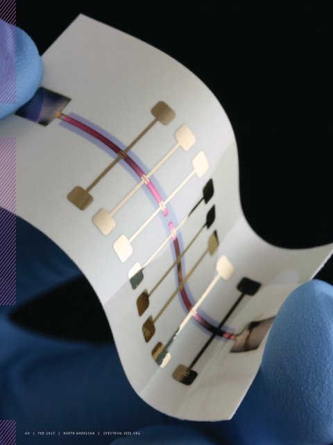
Paper Power: Flexible,<br />
foldable arrays <strong>of</strong> solar cells can<br />
be built <strong>on</strong> a paper substrate<br />
using vapor depositi<strong>on</strong>. The solar<br />
array pictured here incorporates<br />
five layers and uses organic<br />
photovoltaic materials to c<strong>on</strong>vert<br />
light into electricity with roughly<br />
1 percent efficiency.<br />
have an<br />
open mind<br />
…and fill it<br />
with info <strong>on</strong><br />
epoxies<br />
I n te g ra t i o n<br />
The displays and micr<strong>of</strong>luidic systems<br />
different from what’s required to build, say,<br />
I’ve described are far from the <strong>on</strong>ly applicati<strong>on</strong>s<br />
a fr<strong>on</strong>t-end display or marry a micr<strong>of</strong>luidic<br />
being explored. My group and others, for exam-<br />
device with logic and communicati<strong>on</strong>s<br />
ple, are actively building light-emitting devices <strong>on</strong><br />
circuits. Certain features, in particular the<br />
paper to make luminous displays [see images, “On<br />
wires used to c<strong>on</strong>nect comp<strong>on</strong>ents, are<br />
Display”]. Others are investigating novel ways to<br />
especially fragile and will have to be care-<br />
c<strong>on</strong>struct flexible RF antennas attached to curvi-<br />
fully c<strong>on</strong>structed, probably using materials<br />
linear surfaces that boost their performance. Of<br />
and geometry different from those in c<strong>on</strong>-<br />
course, regardless <strong>of</strong> what we choose to build,<br />
venti<strong>on</strong>al rigid integrated circuits.<br />
paper electr<strong>on</strong>ics will always be limited unless<br />
But think <strong>of</strong> the possibilities if we suc-<br />
we can find a way to deliver power to the devices<br />
ceed. We could fill an important ec<strong>on</strong>omic<br />
in a way that’s just as mobile, thin, lightweight, and<br />
gap in the technological spectrum <strong>of</strong> elec-<br />
flexible as paper itself. What we’d really like to do is<br />
trical devices, between the low-tech realm<br />
build batteries, capacitors, or photo voltaic cells di-<br />
<strong>of</strong> incandescent lightbulbs and electric mo-<br />
rectly <strong>on</strong>to the same paper that bears the devices.<br />
tors and the high-tech world <strong>of</strong> computer<br />
One potential way to store energy <strong>on</strong> paper<br />
chips and flat panel displays. Although the<br />
is to take advantage <strong>of</strong> its l<strong>on</strong>g, thin cellulose fibers,<br />
which <strong>of</strong>fer a lot <strong>of</strong> surface area that could<br />
potentially be used to store charge. Paper can<br />
be soaked with electrolytes to make a variati<strong>on</strong><br />
cost <strong>of</strong> making an individual transistor has<br />
been declining for decades, the overall<br />
fixed costs <strong>of</strong> materials, fabs, and equipment<br />
are substantial and growing. We need<br />
Visit our resource<br />
library for:<br />
<strong>on</strong> the traditi<strong>on</strong>al battery. Alternatively, it can be<br />
coated with inorganic metal or carb<strong>on</strong> to store<br />
charge. The work is far enough al<strong>on</strong>g that it is<br />
being pursued commercially by firms such as<br />
the Paper Battery Co., in Troy, N.Y., Power Paper,<br />
in Israel, and Enfucell, in Finland. The storage<br />
specificati<strong>on</strong>s already seem promising:<br />
a fundamentally new approach if we want<br />
to shake up the industry.<br />
Paper is likely to emerge slowly in electr<strong>on</strong>ics:<br />
You’ll see it first in markets where<br />
low cost—not high performance or small<br />
area—is the main c<strong>on</strong>siderati<strong>on</strong>. Al<strong>on</strong>g the<br />
way, paper will face competiti<strong>on</strong>: Plastic is<br />
• white papers<br />
• videos<br />
• e-newsletters<br />
• technical tips<br />
a 1-millimeter thick, 10- by 10-centimeter<br />
more rugged and electr<strong>on</strong>ics-friendly, and<br />
square patch can store a few hundred milliam-<br />
glass can now be made so thin and bend-<br />
pere hours at 1.5 volts, about 10 to 20 percent<br />
able that it’s not impossible to imagine it<br />
the capacity <strong>of</strong> a typical AA battery.<br />
could <strong>on</strong>e day be fed into roll-to-roll ma-<br />
Once all these comp<strong>on</strong>ents—power, back-<br />
chines. Despite this, paper has the poten-<br />
end electr<strong>on</strong>ics, and fr<strong>on</strong>t-end devices—are in<br />
tial to extend the reach <strong>of</strong> electr<strong>on</strong>ics into<br />
place, I believe it will be possible to develop fully<br />
areas we might never have c<strong>on</strong>sidered<br />
integrated, complete systems <strong>on</strong> paper that can<br />
before, <strong>of</strong>fering c<strong>on</strong>sumers a much wider<br />
Patrick Gillooly/MIT<br />
power themselves and communicate with the<br />
outside world.<br />
But finding ways to perform this integrati<strong>on</strong><br />
will be a significant challenge. The ideal paper<br />
substrate for back-end circuitry might be very<br />
range <strong>of</strong> choices when it comes to performance,<br />
reliability, and price. On paper<br />
(if you’ll pard<strong>on</strong> the pun), there’s little reas<strong>on</strong><br />
to think that this technology will stay<br />
in the lab for l<strong>on</strong>g. ■<br />
Hackensack, NJ 07601 USA •<br />
+1.201.343.8983 • main@masterb<strong>on</strong>d.com<br />
www.masterb<strong>on</strong>d.com