A Roadmap and Vision for Physical Design - UCSD VLSI CAD ...
A Roadmap and Vision for Physical Design - UCSD VLSI CAD ...
A Roadmap and Vision for Physical Design - UCSD VLSI CAD ...

Create successful ePaper yourself
Turn your PDF publications into a flip-book with our unique Google optimized e-Paper software.
A <strong>Roadmap</strong> <strong>and</strong> <strong>Vision</strong> <strong>for</strong> <strong>Physical</strong> <strong>Design</strong><br />
Andrew B. Kahng<br />
<strong>UCSD</strong> CSE <strong>and</strong> ECE Depts., La Jolla, CA 92093-0114<br />
abk@ucsd.edu, http://vlsicad.ucsd.edu/<br />
ABSTRACT<br />
This invited paper offers “roadmap <strong>and</strong> vision” <strong>for</strong> physical design.<br />
The main messages are as follows. (1) The high-level roadmap <strong>for</strong><br />
physical design is static <strong>and</strong> well-known. (2) Basic problems remain<br />
untouched by fundamental research. (3) Academia should not overemphasize<br />
back-filling <strong>and</strong> <strong>for</strong>mulation over innovation <strong>and</strong> optimization.<br />
(4) The physical design field must become more mature<br />
<strong>and</strong> efficient in how it prioritizes research directions <strong>and</strong> uses its human<br />
resources. (5) The scope of physical design must exp<strong>and</strong> (up to<br />
package <strong>and</strong> system, down to manufacturing interfaces, out to novel<br />
implementation technologies, etc.), even as renewed focus is placed<br />
on basic optimization technology.<br />
Categories <strong>and</strong> Subject Descriptors<br />
B.7.2 [Integrated Circuits]: <strong>Design</strong> Aids – Layout, Place <strong>and</strong> Route;<br />
F.2.2 [Analysis of Algorithms <strong>and</strong> Problem Complexity]: Non-<br />
Numerical Algorithms <strong>and</strong> Problems – Routing <strong>and</strong> Layout; J.6<br />
[Computer-Aided Engineering]: <strong>CAD</strong><br />
General Terms<br />
Algorithms, <strong>Design</strong><br />
1. PREFACE<br />
This is not a scientific paper - <strong>and</strong> it is more “review <strong>and</strong> commentary”<br />
than “roadmap <strong>and</strong> vision”. References are not intended<br />
to be complete. Many passages are excerpted from material that<br />
I have written <strong>for</strong> the <strong>Design</strong> <strong>and</strong> System Drivers chapters of The<br />
International Technology <strong>Roadmap</strong> <strong>for</strong> Semiconductors (2001 Edition)<br />
[9], <strong>and</strong> several other papers. I am grateful to my coauthors,<br />
to the many individuals who contributed to the 2001 ITRS, <strong>and</strong> to<br />
various copyright-holding entities <strong>for</strong> their indulgence. This paper<br />
would not exist but <strong>for</strong> the kind invitation of Massoud Pedram <strong>and</strong><br />
the ISPD02 program committee, as well as the infinite <strong>for</strong>bearance<br />
of Lisa Tolles-Efinger at Sheridan Printing.<br />
2. WHAT WE NEED<br />
This section gives PD-relevant excerpts from the 2001 ITRS [9].<br />
It should be kept in mind that the ITRS is a statement of technology<br />
Permission to make digital or hard copies of all or part of this work <strong>for</strong><br />
personal or classroom use is granted without fee provided that copies are<br />
not made or distributed <strong>for</strong> profit or commercial advantage <strong>and</strong> that copies<br />
bear this notice <strong>and</strong> the full citation on the first page. To copy otherwise, to<br />
republish, to post on servers or to redistribute to lists, requires prior specific<br />
permission <strong>and</strong>/or a fee.<br />
ISPD’02, April 7-10, 2002, San Diego, Cali<strong>for</strong>nia, USA.<br />
Copyright 2002 ACM 1-58113-460-6/02/0004 ...$5.00.<br />
needs, made to semiconductor supplier industries (of which EDA -<br />
<strong>Design</strong> - is one) by the semiconductor industry. The excerpts here<br />
will draw most heavily from the “logical, physical, <strong>and</strong> circuit design”<br />
section of the 2001 ITRS <strong>Design</strong> chapter. The ITRS taxonomy,<br />
which treats physical design holistically along with logical<br />
<strong>and</strong> circuit design, gives some indication of the appropriate scope<br />
<strong>for</strong> PD. The role of PD is to serve the physical implementation flow,<br />
which serves the system designer: PD enables system-level signoff<br />
into reliable, predictable implementation fabrics.<br />
Nanometer-scale silicon complexity makes it difficult to estimate<br />
<strong>and</strong> abstract the effects of physics <strong>and</strong> embedding on eventual design<br />
quality (timing, power, signal integrity, reliability, manufacturability,<br />
etc.). Hence, logical design <strong>and</strong> eventually system-level<br />
design become more closely linked with PD. The paradigm of hierarchical,<br />
top-down, layout-based implementation planning supported<br />
by a tightly integrated, incremental static (power, timing,<br />
noise) analysis “backplane” is now well-established. Chip implementation<br />
flows will vary according to methodology choices that<br />
juggle process/device abstraction, constraint manipulation, analyses<br />
<strong>and</strong> optimizations in the face of exploding complexities <strong>and</strong> emerging<br />
concerns such as error-tolerance, variability <strong>and</strong> cost.<br />
The following precepts govern future (physical) design technology<br />
innovation. Precepts 3 through 6 are aspects of a (top-down,<br />
iteration-free, decomposition-oriented) “correct by construction” approach.<br />
Precepts 7 <strong>and</strong> 8 are more suited to “construct by correction”,<br />
where iterations are expected but made less painful. Ultimately,<br />
these lead to the future design system architecture depicted<br />
in Figure 1.<br />
1. Exploit reuse.<br />
2. Evolve rapidly. Typical evolutions: (a) analyses evolve into<br />
verifications, which evolve into tests, <strong>and</strong> (b) analyses <strong>and</strong><br />
simulations evolve into models <strong>and</strong> verifications, which evolve<br />
into either objectives or constraints <strong>for</strong> synthesis <strong>and</strong> optimization.<br />
A related trend is “bottom-up commoditization”<br />
(e.g., of characterization <strong>and</strong> RLC extraction, then delay calculation,<br />
static timing / noise analyses, st<strong>and</strong>ard-cell placement,<br />
global routing, ...).<br />
3. Avoid iteration. Iteration between levels of design incurs translation<br />
<strong>and</strong> other interfacing costs, <strong>and</strong> hampers predictability<br />
<strong>and</strong> reliability of the design process.<br />
4. Replace verification by prevention. Lower-level problems (e.g.,<br />
crosstalk-induced delay uncertainty) are more cheaply addressed<br />
by higher-level prevention (e.g., repeater insertion <strong>and</strong> slew<br />
rate control rules).<br />
5. Improve predictability. Constructive estimation does not af<strong>for</strong>d<br />
productivity leverage; efficient search <strong>for</strong> good design so-<br />
112
lutions requires prediction-based estimation. Better estimates<br />
enable design space exploration at higher levels.<br />
6. Orthogonalize concerns (e.g., congestion from timing, timing<br />
from layout, computation from communication). Unrelated<br />
issues should remain separate whenever possible.<br />
7. Exp<strong>and</strong> scope. For example, we require greater integration of<br />
software <strong>and</strong> analog/mixed-signal/RF (AMSRF) design with<br />
digital flows; this must be supported by modeling, analysis<br />
<strong>and</strong> simulation at multiple levels of the system hierarchy (up<br />
to package <strong>and</strong> board, <strong>and</strong> down to mask <strong>and</strong> process).<br />
8. Unify. Silicon complexity induces the unification of previously<br />
disparate areas, e.g., synthesis-analysis, logical-physicaltiming,<br />
or even design-test. Unifications improve the downstream<br />
flow of intentions <strong>and</strong> assumptions, <strong>and</strong> the upstream<br />
flow of estimation/prediction models. Associated frameworks<br />
are successive approximation, <strong>and</strong> incremental optimization.<br />
Increasingly, unifications cross the die-package <strong>and</strong> designmanufacturing<br />
boundaries.<br />
Figure 1: Evolution of design technology.<br />
Specific challenges <strong>for</strong> logical, circuit <strong>and</strong> physical design center<br />
around (1) predictability <strong>and</strong> (2) improved capability to model,<br />
analyze <strong>and</strong> leverage nanometer-scale circuit phenomena. The remainder<br />
of this section flags some of the highlights.<br />
2.1 Predictable Implementation<br />
Scalable, incremental analyses <strong>and</strong> optimizations. PD tools operate<br />
at low levels of abstraction <strong>and</strong> face instance complexities that<br />
grow by at least 2X per technology node. Scalability will require<br />
new ways to manage data, traverse solution spaces, <strong>and</strong> map optimizations<br />
onto distributed/parallel computational resources. To enable<br />
construct-by-correction, we require incremental synthesis <strong>and</strong><br />
analysis capabilities with runtimes proportional to the amount of<br />
change made to the input, <strong>and</strong> with no loss of solution quality. To<br />
enable reuse, we require new measures of solution quality (e.g., stability<br />
or robustness in new environments or when added into other<br />
optimization instances). In addition, chip implementation increasingly<br />
entails large-scale, interacting, multi-level <strong>and</strong> multi-objective<br />
global optimizations; tools will need to generate families of solutions<br />
that capture complex trade-offs among different objectives.<br />
Basic technology needs include techniques <strong>for</strong> constraint-dominated<br />
global optimization, computational resource-bounded optimization,<br />
<strong>and</strong> optimization with partial or probabilistic design in<strong>for</strong>mation.<br />
Unified planning, estimation <strong>and</strong> prediction. Today’s implementation<br />
planning tools create logic <strong>and</strong> timing structure concurrently<br />
with constraint budgets <strong>and</strong> spatial embedding. The st<strong>and</strong>ard approach<br />
combines RT-level floorplanning <strong>and</strong> global interconnect planning<br />
to define repeater insertion <strong>and</strong> pipelining as well as detailed<br />
layout of global signals. The result (after appropriate hierarchy reconciliations)<br />
is passed as a constraint to logic synthesis <strong>and</strong> optimization,<br />
placement <strong>and</strong> routing. PD must enable concurrent system<br />
architecture optimizations that reduce global wires, <strong>and</strong> even<br />
interconnect architecture optimizations that match the number <strong>and</strong><br />
dimensions of wiring layers to the given system. Evolutionary unifications<br />
will continue (layout-clock-test, detailed-routing driven per<strong>for</strong>mance<br />
closure, etc.) to enable the co-optimization depicted in<br />
Figure 1. Since top-down design depends on downstream predictability,<br />
we must more directly seek to define, underst<strong>and</strong> <strong>and</strong> improve<br />
the concept of “predictability” across the entire scope of PD.<br />
Synchronization <strong>and</strong> global signaling. Across-chip communication<br />
requires increasingly many clock cycles; microprocessor global<br />
interconnects are already pipelined <strong>and</strong> are not a limiting factor <strong>for</strong><br />
clock frequency. However, clock distribution in purely synchronous<br />
designs can account <strong>for</strong> over 40% of dynamic power <strong>and</strong> is subject<br />
to increasing stress (e.g., shielding resource requirements, limits of<br />
edge rates <strong>and</strong> jitter, <strong>and</strong> parametric yield loss due to variabilityinduced<br />
skew). There is a clear trend to more robust <strong>and</strong> powerefficient<br />
hybridizations of synchronous <strong>and</strong> asynchronous design,<br />
both GALS (globally asynchronous, locally synchronous) <strong>and</strong> GSLA.<br />
On-chip clock frequencies will vary by two orders of magnitude<br />
or more, <strong>and</strong> reach 15+ GHz; multi-cycle interconnect paths will<br />
be commonplace. PD must deliver <strong>and</strong> support new synchronization<br />
paradigms <strong>for</strong> such regimes. PD must also acknowledge timing<br />
structures wherein “more paths are critical” in the aftermath<br />
of timing <strong>and</strong> power optimizations. The latter phenomenon is accompanied<br />
by quadratically increasing delay sensitivities to process<br />
variation; the need <strong>for</strong> greater margins ultimately limits the return<br />
on traditional delay slack optimization, so new per<strong>for</strong>mance tuning<br />
approaches will be required. On-chip global signaling follows offchip<br />
signaling trends: it increasingly relies on low-swing differential<br />
<strong>and</strong> multi-phase clocking techniques, as well as digital PLL/DLL<br />
synchronization. Improved efficiency <strong>and</strong> signal reliability of traditional<br />
buffered global interconnect must be <strong>for</strong>tified by new syntheses<br />
<strong>and</strong> analyses <strong>for</strong> boosters, state- <strong>and</strong> transition-awareness, multilevel<br />
encoding, time-sharing of interconnect resources, <strong>and</strong> other<br />
emerging signaling paradigms.<br />
Heterogeneity. Single-die integration of analog, mixed-signal <strong>and</strong><br />
RF (AMSRF) with digital logic will challenge PD from planning<br />
through layout. Tools must h<strong>and</strong>le greater sensitivities of, <strong>and</strong> interactions<br />
between, AMSRF circuits with respect to noise <strong>and</strong> interference,<br />
along with constraint-dominated <strong>for</strong>mulations (e.g., matching,<br />
symmetry, <strong>and</strong> electrical rules in layout). Long-term, the integration<br />
of MEMS or other technologies will require novel fault avoidance<br />
<strong>and</strong> fault tolerance methods. On another front, system cost optimizations<br />
(manufacturing cost, <strong>and</strong> the cost of communication) must be<br />
supported by modeling of integration choices that span multi-die<br />
(system-in-package) <strong>and</strong> stacked-die options. Synthesis <strong>and</strong> analy-<br />
113
sis of global signaling must extend to optimization of system-level<br />
interconnect from die through package <strong>and</strong> board.<br />
2.2 The <strong>Design</strong>-Manufacturing Interface<br />
Another aspect of predictability is variability. Atomic-scale effects<br />
increasingly govern the statistics of many process steps, <strong>and</strong><br />
3-sigma variations of such fundamental parameters as L gate , t ox <strong>and</strong><br />
interconnect dimensions now exceed 15%. New circuit topologies<br />
<strong>and</strong> logic/layout optimizations are needed to cope with this level of<br />
variability.<br />
Statistical timing analysis <strong>and</strong> per<strong>for</strong>mance verification must comprehend<br />
parasitics, delays <strong>and</strong> geometrics that are parameterized by<br />
distributions. <strong>Design</strong> centering must optimize <strong>for</strong> parametric yield<br />
<strong>and</strong> revenue per wafer, rather than traditional per<strong>for</strong>mance metrics.<br />
(For example, consider the difference between “L” <strong>and</strong> “staircase”<br />
layouts of a global line with a single repeater, when variabilities<br />
are spatially correlated across the die [8].) Manufacturing variability<br />
(<strong>and</strong> the proliferation of new materials <strong>and</strong> processes) also requires<br />
a more extensive design-manufacturing interface that supplies<br />
design rules <strong>and</strong> process abstractions to layout. Richer statistical<br />
<strong>and</strong> electrical/geometric characterization of manufacturing variability<br />
sources is needed. As power densities continue to rise, naive<br />
guardb<strong>and</strong>ing against thermally induced variability will be costly.<br />
More accurate analyses <strong>and</strong> bounds <strong>for</strong> local thermal variation are<br />
needed to reduce the amount of overdesign.<br />
Reticle enhancement technology (RET) encompasses planarization<br />
of multilayer interconnect processes (necessitating layout density<br />
control with area fill) <strong>and</strong> deep-subwavelength optical lithography<br />
(necessitating optical proximity corrections (OPC) <strong>and</strong> layout<br />
of alternating-aperture phase-shifting masks (PSM)). RET places a<br />
growing burden on physical design with respect to layout design<br />
complexity, manufacturing h<strong>and</strong>off complexity, <strong>and</strong> manufacturing<br />
(mask) NRE cost. With OPC <strong>and</strong> PSM, layout synthesis productivity<br />
is challenged by complex, context-dependent design rules. Layout<br />
verification must also h<strong>and</strong>le regimes where “local design rules”<br />
no longer exist. <strong>Physical</strong> verification must accurately underst<strong>and</strong><br />
<strong>and</strong> model, e.g., the RLC extraction impact of downstream dummy<br />
metal insertion in the post-tapeout layout database.<br />
Indiscriminate application of RET explodes data volumes <strong>and</strong> mask<br />
write/inspection costs. RET insertion (<strong>and</strong> mask inspection) must<br />
there<strong>for</strong>e underst<strong>and</strong> that only certain critical device or interconnect<br />
dimensions are worth the expense of careful en<strong>for</strong>cement, <strong>and</strong> that<br />
some en<strong>for</strong>cement mechanisms are costlier to implement <strong>and</strong> verify<br />
than others. A data volume- <strong>and</strong> cost-sensitive PD flow will enable<br />
such selectivity by passing detailed functional intent, per<strong>for</strong>mance<br />
analysis results, <strong>and</strong> sensitivities <strong>for</strong>ward throughout the layout, verification<br />
<strong>and</strong> mask flows.<br />
2.3 Silicon Complexity <strong>and</strong> Non-Ideal Scaling<br />
Lower supply voltages, along with larger currents stemming from<br />
increased power densities, lead to larger relative supply rail inductive<br />
noise. This is exacerbated by less aggressive scaling of bump<br />
counts <strong>and</strong> pitches. Issues such as IR drop <strong>and</strong> decoupling capacitance<br />
have been addressed in the recent PD literature. Near-term<br />
open issues include control of temperature variation across the die<br />
<strong>for</strong> package <strong>and</strong> per<strong>for</strong>mance reliability. This entails new tools spanning<br />
algorithm development, logic synthesis, <strong>and</strong> timing/layout optimization<br />
that must cooperate to manage both instantaneous <strong>and</strong> average<br />
power. The large estimated “power management gap” <strong>for</strong> microprocessor<br />
<strong>and</strong> SOC system drivers implies a continual focus on<br />
power reduction. At the PD level, library characterization, synthesis,<br />
<strong>and</strong> layout (including power distribution design) must together<br />
deliver the roughly 5X available power reduction from fine-grain<br />
use of multiple thresholds <strong>and</strong> supplies (<strong>and</strong> oxide thicknesses, <strong>and</strong><br />
biasing) in the same core. Potentially, PD tools must automatically<br />
produce structures that enable active thermal management via OSmediated<br />
dynamic frequency <strong>and</strong> supply scaling.<br />
Reliability <strong>and</strong> fault-tolerance. Reliability criteria (hot-carrier effect,<br />
electromigration, joule self-heating, etc.) have been integrated<br />
into implementation flows via simple <strong>and</strong> transparent abstractions<br />
(e.g., upper bounds on gate load capacitance vs. output slew time).<br />
Such “methodological” abstractions currently permit correctness by<br />
construction with little disruption of traditional flows. However,<br />
improved abstractions <strong>and</strong> analyses that reduce guardb<strong>and</strong>ing will<br />
be needed in the future. With respect to single-event upsets (SEU)<br />
caused by ionizing radiation, decreasing feature sizes lower Q crit<br />
values to such levels that even the noise pulse from an alpha particle<br />
can be trapped as a logic fault. Automated methods are needed to<br />
modify logical, circuit <strong>and</strong> physical design (e.g., by automatic introduction<br />
of error correction, sizing, etc.) to prevent or manage SEU<br />
without violating design constraints.<br />
2.4 Circuit Implementation<br />
Non-ideal scaling impacts (notably from scaling supplies faster<br />
than thresholds) include higher gate <strong>and</strong> drain leakage currents, body<br />
effect (making pass gate logic less attractive), <strong>and</strong> loss of overdrive.<br />
In light of power management challenges, past tradeoffs of higher<br />
power <strong>and</strong> noise susceptibility (along with unavailability of automated<br />
tools) in return <strong>for</strong> speed become less attractive. As alternatives<br />
to static CMOS are deployed to permit overall speed/power<br />
per<strong>for</strong>mance gains, layout automation <strong>and</strong> physical verification (e.g.,<br />
automated extraction of novel active <strong>and</strong> passive structures from layout)<br />
will be needed. For example, self-sufficient circuits such as<br />
clock-delayed domino or delayed-reset domino will become more<br />
popular with use of globally synchronous, locally asynchronous architectures.<br />
Circuit modeling must be consumable at ever-higher<br />
levels, as systems move to compiler- <strong>and</strong> OS-based control of such<br />
parameters as body bias, clock, <strong>and</strong> supply rails. For SOI, PD has<br />
already made progress toward necessary analyses (e.g., historydependence<br />
of timing, coupling dependence of static power) <strong>and</strong><br />
syntheses (e.g., planning of decoupling capacitance).<br />
Analog synthesis. Scaling of SOC design productivity requires<br />
elimination of today’s “analog design bottleneck”. Existing specialized<br />
circuit syntheses <strong>for</strong> particular classes of circuits (PLL, opamp,<br />
power amplifier, etc.) must be augmented by more general<br />
techniques as well as automatic layout syntheses. Analog syntheses<br />
must h<strong>and</strong>le increased opportunities <strong>for</strong> distortion <strong>and</strong> nonlinearity<br />
due to impact ionization, thermal nonlinearity, body contacts acting<br />
as b<strong>and</strong>pass filters, etc. Syntheses must also h<strong>and</strong>le future regimes<br />
of increased manufacturing variability, e.g., by hybrid analog-digital<br />
compensation <strong>for</strong> device mismatch. Isolation techniques must be<br />
flexibly applied. In the near term, new synthesis tools <strong>for</strong> optical<br />
interface circuits <strong>and</strong> high-Q tunable CMOS on-chip inductors/resonators<br />
are needed. Circuit types of interest in the long term<br />
include extremely low-power sensing <strong>and</strong> sensor interface circuits,<br />
as well as micro-optical (e.g., beam-steering) devices. Due to the<br />
difficulty of analog verification <strong>and</strong> testing, BIST circuitry will be<br />
increasingly synthesized around, <strong>and</strong> laid out with, analog circuitry<br />
such as high-speed networking interfaces. Such techniques must<br />
be nonintrusive, i.e., they cannot degrade per<strong>for</strong>mance of embedded<br />
analog blocks.<br />
3. WHAT WE DO<br />
According to Dataquest, EDA as a whole has less than 6,000<br />
R&D engineers worldwide. Total tools revenue per designer has<br />
114
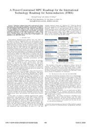
Topic 1996 1997 1998 1999 2000 2001<br />
1 4/4/7 8/10/6 4/5/7.5 5/5.5/3 4.5/6/5 3/4.5/8<br />
2 0/4/3 1/0.5/2 3/2/4 3.5/1/5 4.5/4/4 0/5.5/3.5<br />
3 2/1/3 2/0/1 2/1/3 1.5/2/1 0/0/2 2/0/0<br />
4 1/1/2 1/1/2.5 0/5/2 2.5/2/3 2/0/5 2/0/4<br />
5 4.5/3.5/2.5 0.5/4/3 0/2/2.5 4/4.5/2.5 2/3/2+1 0/0.5/4<br />
6 0/0/1 0/0/1 2/0/1.5 1/0/0 1/0/1+1 0/1/0<br />
7 3/2.5/0 1/1.5/1 0/0/0.5 0.5/0.5/3 1/0/0+1 0/1.5/0<br />
8 0/1.5/2 0.5/2/1 1/0/1.5 1.5/0/0 0/2/4+2 0/1/1+2<br />
9 2.5/0/2 7/0/0 0/6/0 1/1.5/0.5 0/0/0 0/0.5/0<br />
10 0/0/0 0/0/1.5 0/4/0 2/0/1 0/0/0 0/2/0<br />
11 1/2/0 1/0/2 0/0/1 0/0/1 3/1/1+3 0+5/0/1<br />
12 0/0.5/1.5+2 2/0/0 0/0/0 0/0/0 1/2/0 0/0/1<br />
13 0/0/0 0/0/1 1/3/3.5 1/0/4 0/0/0 0/0.5/1.5<br />
Table 1: Distribution of physical design papers among 13 topics,<br />
<strong>for</strong> cycles of DAC(Y)/IC<strong>CAD</strong>(Y)/ISPD(Y+1) with Y = 1996, ...,<br />
2001. Invited papers are indicated by (+). Data compiled by Bao<br />
Liu, Swamy Muddu <strong>and</strong> Puneet Gupta.<br />
increased at 3.9% per year on average <strong>for</strong> the past decade [9, 15].<br />
Pure research investment is low relative to other semiconductor supplier<br />
industries (my estimate is in the tens of millions of dollars per<br />
year).<br />
In the overall history of EDA, physical design has played a very<br />
large <strong>and</strong> critical role. However, most of today’s design technology<br />
“crises” – verification, embedded software <strong>and</strong> system-level design,<br />
enabling of power management at the architectural <strong>and</strong> operatingsystem<br />
levels, analog/mixed-signal synthesis <strong>and</strong> reuse, design <strong>for</strong><br />
test – lie elsewhere. The ratio of design value over ef<strong>for</strong>t is perceived<br />
to decrease as the level of abstraction moves from behavior<br />
down to layout. Thus, PD is now just another piece (say, at most<br />
one-sixth, whether by market size or by headcount) of EDA <strong>and</strong> design<br />
technology as a whole. PD researchers, developers <strong>and</strong> funding<br />
are not plentiful resources. With this as backdrop, let us now consider<br />
the distribution of PD research activity relative to PD roadmap<br />
needs.<br />
Certainly, there are critical design technology requirements that<br />
can <strong>and</strong> must be addressed by physical design research. Examples<br />
include analog layout synthesis <strong>and</strong> reuse; layout-BIST synergies<br />
<strong>for</strong> “deep-submicron fault models”; new paradigms <strong>for</strong> global<br />
signaling, synchronization <strong>and</strong> system-level interconnect; modeling<br />
<strong>and</strong> simulation; mitigation of increased process variability <strong>and</strong> nonrecurring<br />
costs in the mask <strong>and</strong> foundry flows; <strong>and</strong> multi-(V dd , V t ,<br />
t ox , biasing) per<strong>for</strong>mance optimization. Yet, there is a clear mismatch<br />
between these needs <strong>and</strong> the core of PD research activity as<br />
defined by the technical program committees of ISPD <strong>and</strong> other major<br />
conferences.<br />
Table 1 shows results of a cursory scan of DAC, IC<strong>CAD</strong> <strong>and</strong> ISPD<br />
program content to assess the relative prominence of 13 topic areas<br />
in physical design. 1 The 13 topic areas are: (1) placement / partitioning;<br />
(2) routing / global routing / wireplanning; (3) interconnect<br />
tree (buffered / Steiner / RAT / etc.) construction; (4) floorplanning<br />
/ block packing / macro-cell placement; (5) per<strong>for</strong>mance optimization<br />
(sizing, etc.); (6) RTL-down methodology / flow; (7) clock; (8)<br />
power; (9) custom layout (transistor-level / migration / compaction);<br />
(10) analog; (11) manufacturability / yield; (12) logical-physical interactions;<br />
<strong>and</strong> (13) signal integrity. 2 The Table shows that most<br />
1 Other analyses are also possible, e.g., of paper submission statistics<br />
or measures of “scientific health” (cf., e.g., [21, 20]).<br />
2 In recent years, papers on logical-physical interactions (12) have<br />
shifted to, <strong>and</strong> are tallied in, the more specific planning (2) <strong>and</strong> RTLdown<br />
methodology (6) topic areas. Papers on signal integrity (13)<br />
have <strong>for</strong> the most part shifted to the global <strong>and</strong> detailed routing (2)<br />
“classical” (1-5) topic areas still receive the bulk of the community’s<br />
attention. Custom layout (9) is “classical” as well, but has not<br />
been a substantial part of the literature in recent years. ISPD <strong>and</strong> IC-<br />
<strong>CAD</strong> seem to publish more papers on “classical” topics than DAC.<br />
Non-classical issues are typically visible only in isolated years.<br />
Looking backward, 1997 <strong>and</strong> 1998 may have displayed greater<br />
shifts in attention, with several paper slots dedicated to emerging<br />
topics (methodology, signal integrity, custom layout, analog physical<br />
design automation, etc.). However, these topic areas quickly<br />
lost steam, <strong>and</strong> today analog design, clocking, custom layout, <strong>and</strong><br />
manufacturability are all research holes that have become critical to<br />
industry. (In 2000 <strong>and</strong> 2001, the emerging topic appears to be (11)<br />
manufacturability <strong>and</strong> yield. But despite PDW96’s special session<br />
on yield <strong>and</strong> ISPD99’s invited tutorial on subwavelength lithography<br />
[14], ISPD01 invited three of its four papers on this topic, <strong>and</strong><br />
DAC01 invited all five of its manufacturability papers. 3 ) It is reasonable<br />
to conclude from the Table that the scope of PD has remained<br />
fairly stable, with certain semiconductor industry needs remaining<br />
under-resourced. In light of ITRS needs, PD researchers should exp<strong>and</strong><br />
the scope of physical design up to package <strong>and</strong> system, down<br />
to manufacturing interfaces, out to novel device/circuit implementation<br />
technologies, <strong>and</strong> back to analog <strong>and</strong> custom layout.<br />
What Is Going On Here?<br />
Table 1 is, by itself, not surprising. Consider the following explanations.<br />
(1) There are long lead times <strong>and</strong> latencies as research moves<br />
from problem <strong>for</strong>mulation to solution to technology transfer to marketplace.<br />
(2) Critical research topics can have greater startup costs<br />
or other barriers to entry. (3) Any research field will tend to recreate<br />
itself in its own image <strong>and</strong> perpetuate its prevailing st<strong>and</strong>ards<br />
(e.g., via program committees <strong>and</strong> following of research threads).<br />
These are inefficiencies which neither the PD field nor the semiconductor<br />
industry can af<strong>for</strong>d. The first two inefficiencies are highly<br />
pernicious, but can be addressed by a “coopetitive” mindset change<br />
as outlined in the next section. The third inefficiency merits a few<br />
comments in the remainder of this section.<br />
¯ It’s not as if we are failing to hit a moving target: the target<br />
is in the open <strong>and</strong> it’s st<strong>and</strong>ing still. 4 More specifically, the<br />
physical design roadmap has been static <strong>for</strong> quite a few years.<br />
Key goals such as (1) convergent integration of logical, timing<br />
<strong>and</strong> spatial embedding, or (2) unification of incremental timing/SI<br />
closure with a per<strong>for</strong>mance analysis backplane, have<br />
been in the NTRS/ITRS since 1997 (<strong>and</strong> in Sematech’s CHDS<br />
requirements as of 1995). Most of the methodology precepts<br />
<strong>and</strong> physical design requirements have been stated since the<br />
1997 NTRS, <strong>and</strong> arguably since the 1994 NTRS. The modern<br />
methodology <strong>and</strong> routing contexts are quite close to what was<br />
described in [3, 10]. The 2001 ITRS litany of manufacturability<br />
challenges reiterates an ISPD99 presentation [14].<br />
¯ We may be spending too much ef<strong>for</strong>t on “back-filling” of<br />
well-known issues <strong>and</strong> already-commercialized techniques into<br />
the public literature. In my past work, [7] is an example, albeit<br />
made with good intentions. Today’s st<strong>and</strong>ardized planning<br />
framework (cf. [9, 10, 3]) has commercial implementations<br />
[26, 27, 28] that - in terms of infrastructure, functionality <strong>and</strong><br />
evaluatability - are superior to what academia can likely manage.<br />
“Classic” multi-stage approaches to large-scale fixed-die<br />
topic area. Each topic area makes its own advances.<br />
3 Guess who organized these sessions :-) .<br />
4 It’s not as if I am saying anything new: Lou Scheffer has provided<br />
a similar roadmap <strong>and</strong> message 5-6 years ago [22, 23].<br />
115
outing are also better implemented in industry. Melding hierarchical<br />
graph-based layout resource abstractions [24, 18,<br />
25] with shape-based detailed routing [3] is now st<strong>and</strong>ard in<br />
industry, but may not be worth developing in academia. The<br />
value of “back-filling”, aside from impact on IP, is unclear to<br />
me; I believe that more industry-strength shared infrastructures<br />
should have higher priority.<br />
¯ Is the goal of research novelty in “<strong>for</strong>mulation”, or novelty<br />
in “optimization”? To be provocative, I will claim that PD is<br />
tending to focus more on new problem statements, while only<br />
transferring or reusing core optimization techniques. 5 However,<br />
representation <strong>and</strong> <strong>for</strong>mulation are not the end goal (e.g.,<br />
[10] noted a “packing obsession” (really, representation obsession)<br />
which has been worked-around in industry by hierarchical<br />
coarse placement). We have no shortage of problems;<br />
we have a shortage of optimization tools from which we can<br />
create solutions.<br />
4. WHAT WE NEED TO DO<br />
This section describes two “mindset changes”. The first, “coopetition”,<br />
addresses two inefficiencies mentioned in the previous section<br />
<strong>and</strong> opens the door to greater effectiveness <strong>and</strong> impact of the<br />
PD field. The second, “shared red bricks”, opens the door to greater<br />
rewards <strong>for</strong> greater impact of the PD field in furthering the semiconductor<br />
roadmap.<br />
4.1 Coopetition<br />
Phrases such as “design productivity gap” (stemming from a 1994<br />
Sematech presentation, <strong>and</strong> propagated through several editions of<br />
the NTRS/ITRS) <strong>and</strong> the existence of the MARCO <strong>Design</strong> <strong>and</strong> Test<br />
Focus Research Center (www.gigascale.org) reflect a perceived need<br />
to improve the effectiveness of <strong>CAD</strong> research. In 1999, the <strong>Design</strong><br />
Automation Conference instituted a new topic area: “Fundamental<br />
<strong>CAD</strong> Algorithms”. In the area of hypergraph bipartitioning,<br />
[5] noted that silent, undocumented implementation decisions could<br />
change result quality by more than 400% - <strong>and</strong> that contemporaneous<br />
papers reported more than 1,000% differences in solution costs<br />
returned by implementations of the same well-known algorithm. To<br />
help the <strong>CAD</strong> community address these problems, a new medium<br />
<strong>for</strong> <strong>CAD</strong>-IP reuse - thus far centered in the PD domain - has been<br />
established under the auspices of the MARCO Gigascale Silicon Research<br />
Center (http://www.gigascale.org/) [6]. Called the MARCO<br />
GSRC Bookshelf, it serves as a clearinghouse <strong>and</strong> a repository <strong>for</strong><br />
intellectual property in <strong>CAD</strong>. 6<br />
Motivations <strong>for</strong> <strong>CAD</strong>-IP reuse include the following. (1) Better<br />
software development processes can improve productivity. Expected<br />
time to completion grows with project risk, which in turn<br />
grows with the amount of code that must be written from scratch.<br />
5 Fifteen or more years ago, PD was the source of simulated annealing,<br />
the LP relaxation <strong>and</strong> rounding framework, hierarchical routing<br />
[4], etc. Force-directed placement is a decades-old framework [19].<br />
In recent years - <strong>and</strong> I again look to my own works <strong>for</strong> examples -<br />
I feel that PD has been more in the mode of transferring methods<br />
(e.g., multilevel in [1] <strong>and</strong> then [2, 16], various numerical methods,<br />
etc.). Fundamental new optimization approaches have not appeared<br />
in recent years, but seem overdue in light of new computational plat<strong>for</strong>ms,<br />
new instance scales, <strong>and</strong> new objectives.<br />
6 The Bookshelf is one of three initiatives - along with technology<br />
extrapolation (a “living roadmap”) <strong>and</strong> measurement infrastructure<br />
to support design process improvement (“metrics”) - in<br />
the GSRC’s “Calibrating Achievable <strong>Design</strong>” (“C.A.D.”) research<br />
theme (http://vlsicad.ucsd.edu/GSRC/) that together seek to improve<br />
design technology productivity.<br />
Cheaply reusing existing codes with documented per<strong>for</strong>mance <strong>and</strong><br />
a history of successful reuse can reduce risk <strong>and</strong> shorten time to market<br />
even if new features or interfaces must be added. (2) Evaluation<br />
of result quality requires thorough underst<strong>and</strong>ing of algorithms <strong>and</strong><br />
software tools, including common benchmarks, evaluation methodologies,<br />
<strong>and</strong> known-good per<strong>for</strong>mance results. Episodes in hypergraph<br />
partitioning cited in [5] show the risks when any aspect of a<br />
sophisticated technology’s leading edge is unclear. Such risks increase<br />
as a research domain matures <strong>and</strong> the literature exp<strong>and</strong>s - in<br />
other words, as a problem gains importance <strong>and</strong> attention. When<br />
individual researchers can no longer keep track of all relevant research,<br />
there is a risk of poor reinvention of the wheel, <strong>and</strong> slower<br />
overall progress in the field. A partial remedy is to leverage community<br />
resources in verifying per<strong>for</strong>mance claims <strong>and</strong> implementations.<br />
(3) EDA research tends to focus on narrow optimizations, e.g.,<br />
netlist hypergraph partitioning in physical design. If this narrowness<br />
is accompanied by the inability to evaluate new results in the context<br />
of full design flows, the utility of research decreases. (4) For mature,<br />
nondifferentiating technologies whose details do not affect competitiveness<br />
in the marketplace, reimplementation incurs tremendous<br />
waste. Resource imperatives eventually <strong>for</strong>ce data models, polygon<br />
database implementations, placers <strong>and</strong> routers, etc. to evolve into<br />
nondifferentiating, commoditized (but nearly free) “foundation IP”<br />
(following the course of operating systems, data structures, <strong>and</strong> GUI<br />
components be<strong>for</strong>e them). This evolution is consistent with the culture<br />
of “coopetition” (collaboration among competitors) exemplified<br />
by consortia such as Sematech.<br />
<strong>Design</strong>ers <strong>and</strong> researchers need an infrastructure that clearly identifies<br />
the best results in the <strong>CAD</strong> field at any given time. Such an<br />
infrastructure should reuse accumulated knowledge about st<strong>and</strong>ard<br />
benchmarks, evaluation methodologies, <strong>and</strong> per<strong>for</strong>mance comparisons.<br />
This goes beyond mere code reuse <strong>and</strong> entails more general<br />
reuse of <strong>CAD</strong>-IP. The GSRC Bookshelf to date includes 28 distinct<br />
“slots” (areas of <strong>CAD</strong>-IP) ranging from single interconnect tree synthesis<br />
to st<strong>and</strong>ard-cell placement to vertical benchmark designs. In<br />
effect, the Bookshelf is a new “publication medium” that offers a<br />
unique combination of emphases: algorithmic <strong>CAD</strong> IP, advancement<br />
of leading-edge design technology, free reuse, comparison <strong>and</strong><br />
evaluation methodologies, <strong>and</strong> common data modeling. Ongoing<br />
work 7 under the auspices of the MARCO GSRC aims to build the<br />
Bookshelf’s content <strong>and</strong> breadth, <strong>and</strong> to make the Bookshelf an integral<br />
part of the research process within the design technology community.<br />
4.2 Shared Red Bricks<br />
As noted in [11, 12, 13] the ITRS defines a “red brick” as a “technology<br />
requirement <strong>for</strong> which no known solution exists”. Solving<br />
any given red brick is expensive, <strong>and</strong> requires large R&D investments.<br />
The ITRS is now full of red bricks, to the extent that these<br />
red bricks seem to <strong>for</strong>m a “red brick wall” in the not too distant future.<br />
8 My contention is that many red bricks stem from trying to<br />
continue old ways or old trends without seeking synergy with other<br />
parts of the semiconductor supply chain. 9 We need a more globally<br />
7 E.g., building new linkages among Bookshelf slots, common data<br />
models, <strong>and</strong> industrial data interchange <strong>for</strong>mats to enable vertical<br />
benchmarking <strong>and</strong> more complete evaluation of algorithm innovations.<br />
8 In the 1999 ITRS, the red brick wall with respect to overlay accuracy,<br />
CD control, equivalent oxide thickness, <strong>and</strong> ILD permittivity<br />
appeared to be between six <strong>and</strong> nine years away. In the 2001 ITRS,<br />
these red bricks appear to be between four <strong>and</strong> six years away.<br />
9 The following metaphor may help to clarify this point. Think of<br />
the ITRS - the semiconductor industry’s technology foundations -<br />
116
optimized allocation of R&D investments, i.e., “shared red bricks”.<br />
Three examples of potential shared red bricks are as follows. (1)<br />
Must lithography, front-end processes, <strong>and</strong> interconnect technologies<br />
continue to push <strong>for</strong> 10% tolerances in critical dimensions?<br />
This would mean gate length <strong>and</strong> oxide thickness tolerances in the<br />
range of a single atomic monolayer by the end of the roadmap. Or<br />
are there design-<strong>for</strong>-variability solutions that share the red brick of<br />
variability between <strong>Design</strong> <strong>and</strong> these other industries? The first generation<br />
of variability-aware analysis tools is available now. However,<br />
variability-aware synthesis tools (centering <strong>for</strong> robustness under<br />
variability, or <strong>for</strong> maximum $/wafer) are a long ways off. Appropriate<br />
(<strong>and</strong> st<strong>and</strong>ardized) characterizations of variability sources<br />
in manufacturing equipment <strong>and</strong> processes also appear to be a long<br />
ways off. Circuit <strong>and</strong> layout techniques <strong>for</strong> high-variability regimes<br />
must also be explored. (2) Should the industry build new, faster<br />
mask writers that can h<strong>and</strong>le 250 Gbytes of data <strong>for</strong> a single mask<br />
layer, after optical proximity correction (OPC) <strong>and</strong> fracturing? Or,<br />
should the industry reduce data volumes <strong>and</strong> relax inspection tolerances<br />
- thus improving mask throughput, yield, <strong>and</strong> cost - by exploiting<br />
design hierarchy <strong>and</strong> an awareness of which features are<br />
functionally critical? (3) Do we really need dielectric permittivities<br />
below 2.0 or copper interconnect resistivities below 1.8 mΩ-cm, as<br />
specified in the ITRS? Is the latter even possible? Would developing<br />
better circuit <strong>and</strong> interconnect architectures, <strong>and</strong> better layout<br />
techniques (cf. the X Initiative [29]), more cost-effectively share<br />
per<strong>for</strong>mance <strong>and</strong> noise management red bricks between <strong>Design</strong> <strong>and</strong><br />
Interconnect technologies?<br />
These examples highlight the potential of deeper partnerships between<br />
design technology <strong>and</strong> other ITRS technology industries. The<br />
key observation is that PD is the interface to circuits, devices, materials,<br />
<strong>and</strong> packaging; PD is there<strong>for</strong>e at the heart of nearly all such<br />
potential partnerships. Since such partnerships can potentially resolve<br />
key red bricks at greatly reduced cost to the semiconductor<br />
industry, it would be natural <strong>for</strong> PD to pursue not only shared solutions<br />
but also a share of the R&D investment reward.<br />
5. WHAT WE NEED TO DO, II<br />
This concluding section of “key directions” will need to be short.<br />
(0) Sensible unifications (sub-flows) that truly co-optimize global<br />
signaling, manufacturability enhancement, <strong>and</strong> clock/test/power distribution.<br />
(1) Fundamental new combinatorial optimization technologies,<br />
<strong>and</strong> possibly geometry engines, <strong>for</strong> future constraintdominated<br />
layout regimes. (2) New decomposition schemes <strong>for</strong><br />
physical design. (3) Global routing that is truly path-timing aware,<br />
truly combinatorial, <strong>and</strong> able to invoke “atomistic” interconnect synthesis.<br />
(4) In-context layout synthesis that maximizes process window<br />
while meeting electrical (functional) spec, <strong>and</strong> is able to h<strong>and</strong>le<br />
restricted geometries (<strong>for</strong>bidden widths/pitches, on-grid constraints<br />
[17], halation rules). (5) Efficient analog <strong>and</strong> mixed-signal layout<br />
synthesis. (6) Methods <strong>for</strong> synchronization <strong>and</strong> global signaling<br />
at multi-GHz or -Gbps, extending to system-level integration. (7)<br />
New analysis, modeling <strong>and</strong> simulation methods that are tied more<br />
closely to PD syntheses, <strong>and</strong> that adapt to resource <strong>and</strong> accuracy /<br />
as a car. The supplier industries (packaging, lithography, design,<br />
etc.) are the parts of the car. The car must continue to be driven<br />
along the Moore’s Law road, e.g., if the car goes 150mph today then<br />
four years from now we require the car to reach speeds of 600mph.<br />
It is absurd to think that super tires alone, or super seats alone, will<br />
get us to 600mph. However, the seat industry might specify its requirements,<br />
<strong>and</strong> the concomitant levels of R&D investment, from<br />
the perspective that super seats alone must enable the 600mph car!<br />
It is economically wasteful <strong>and</strong> technologically impossible <strong>for</strong> each<br />
supplier industry to attempt to continue Moore’s Law all by itself.<br />
fidelity constraints. (8) Revival of plat<strong>for</strong>m-specific (parallel, distributed,<br />
hardware-accelerated) algorithm implementations. (9)<br />
Mindset changes as described in Section 4, <strong>and</strong> a new culture of<br />
“duplicating, deconstructing <strong>and</strong> debunking” [30].<br />
6. REFERENCES<br />
[1] C. J. Alpert, L. Hagen <strong>and</strong> A. B. Kahng, “A Hybrid Multilevel/Genetic<br />
Approach <strong>for</strong> Circuit Partitioning”, Proc. ACM SIGDA <strong>Physical</strong> <strong>Design</strong><br />
Workshop, April 1996, pp. 100-105.<br />
[2] C. J. Alpert, J. H. Huang <strong>and</strong> A. B. Kahng, “Multilevel Circuit Partitioning”,<br />
Proc. ACM/IEEE <strong>Design</strong> Automation Conf., 1997, pp. 530-533.<br />
[3] R. Brashears <strong>and</strong> A. B. Kahng, “Advanced Routing <strong>for</strong> Deep Submicron<br />
technologies”, Computer <strong>Design</strong>, May 1997. http://www.computerdesign.com/Editorial/1997/05/supplement/597suprouting.html<br />
[4] M. Burstein <strong>and</strong> R. Pelavin, “Hierarchical Wire Routing”, IEEE Trans. <strong>CAD</strong><br />
2(4) (1983), pp. 223-34.<br />
[5] A. E. Caldwell, A. B. Kahng, A. A. Kennings <strong>and</strong> I. L. Markov, “Hypergraph<br />
Partitioning <strong>for</strong> <strong>VLSI</strong> <strong>CAD</strong>: Methodology <strong>for</strong> Reporting, <strong>and</strong> New Results”,<br />
Proc. ACM/IEEE <strong>Design</strong> Automation Conf., June 1999, pp. 349-354.<br />
[6] A. E. Caldwell, A. B. Kahng <strong>and</strong> I. L. Markov, “Toward <strong>CAD</strong>-IP Reuse: A Web<br />
Bookshelf of Fundamental <strong>CAD</strong> Algorithms”, IEEE <strong>Design</strong> <strong>and</strong> Test, May<br />
2002.<br />
[7] A. E. Caldwell, A. B. Kahng <strong>and</strong> I. L. Markov, “Can Recursive Bisection Alone<br />
Produce Routable Placements?”, Proc. ACM/IEEE <strong>Design</strong> Automation Conf.,<br />
2000, pp. 477-482. (Cf. the “quadratic placement revisited” work as well.)<br />
[8] Y. Cao, P. Gupta, A. B. Kahng, D. Sylvester <strong>and</strong> J. Yang, “Toward a Framework<br />
<strong>for</strong> Assessing the Impact of Variability in Nanometer <strong>Design</strong>”, manuscript,<br />
2001.<br />
[9] The International Technology <strong>Roadmap</strong> <strong>for</strong> Semiconductors, 2001 edition,<br />
International Sematech, Austin, Texas, December 2001. http://public.itrs.net/<br />
[10] A. B. Kahng, “Classical Floorplanning Harmful?”, Proc. Intl. Symp. on<br />
<strong>Physical</strong> <strong>Design</strong>, April 2000, pp. 207-213. See talk slides at<br />
http://vlsicad.ucsd.edu/papers/slides/ispd00-cfh.ppt<br />
[11] A. B. Kahng, “<strong>Design</strong>-Process Integration <strong>and</strong> Shared Red Bricks”, Proc.<br />
<strong>Design</strong> <strong>and</strong> Process Integration <strong>for</strong> Microelectronic Manufacturing, SPIE vol.<br />
4692, March 2002.<br />
[12] A. B. Kahng, “The Road Ahead” (column), IEEE <strong>Design</strong> <strong>and</strong> Test, 2002.<br />
[13] A. B. Kahng, various talks, http://vlsicad.ucsd.edu/˜abk/TALKS/ .<br />
[14] A. B. Kahng <strong>and</strong> Y. C. Pati, “Subwavelength Optical Lithography: Challenges<br />
<strong>and</strong> Impact on <strong>Physical</strong> <strong>Design</strong>”, Proc. Intl. Symp. on <strong>Physical</strong> <strong>Design</strong>, April<br />
1999, pp. 112-119. See<br />
http://vlsicad.ucsd.edu/ISPD99TUTORIAL/ispdtutorial.ppt (similar<br />
presentation material is in<br />
http://vlsicad.ucsd.edu/ISQED00TUTORIAL/isqed2000tutorial-abk.ppt).<br />
[15] A. B. Kahng <strong>and</strong> G. Smith, “A New <strong>Design</strong> Cost Model <strong>for</strong> the 2001 ITRS”,<br />
Proc. ISQED, March 2002.<br />
[16] G. Karypis, R. Aggarwal, V. Kumar <strong>and</strong> S. Shekhar, “Multilevel Hypergraph<br />
Partitioning: Application in <strong>VLSI</strong> Domain”, Proc. ACM/IEEE <strong>Design</strong><br />
Automation Conference, 1997, pp. 526-529.<br />
[17] M. D. Levenson, J. S. Petersen, D. G. Gerold <strong>and</strong> C. A. Mack, “Phase Phirst!<br />
An Improved Strong-PSM Paradigm”, Proc. 20th Annual BACUS Symposium<br />
on Photomask Technology, Monterey, CA, USA, 13-15 Sept. 2000, SPIE vol.<br />
4186, pp. 395-404.<br />
[18] R. Nair, “A Simple Yet Effective Technique <strong>for</strong> Global Wiring”, IEEE Trans. on<br />
<strong>CAD</strong> 6(6) (1987), pp. 165-172.<br />
[19] N. R. Quinn <strong>and</strong> M. A. Breuer, “A Force-Directed Component Placement<br />
Procedure <strong>for</strong> Printed Circuit Boards”, IEEE Trans. on Circuits <strong>and</strong> Systems<br />
26(6) (1979), pp. 377-88.<br />
[20] S. Savage, “On the Biodiversity of SIGCOMM”, 2000 ACM SIGCOMM<br />
Outrageous Opinions, Stockholm, Sweden, August 2000.<br />
[21] S. Savage, “On the Caching <strong>and</strong> Prefetching of Program Committees”, 1999<br />
ACM SIGCOMM Outrageous Opinions, Cambridge, MA, September 1999.<br />
[22] L. Scheffer, “We’re Solving the Wrong Problems”, Proc. 6th <strong>Physical</strong> <strong>Design</strong><br />
Workshop, April 1996, Reston, Virginia, pp. 89-91.<br />
[23] L. Scheffer, “A <strong>Roadmap</strong> of <strong>CAD</strong> Tool Changes <strong>for</strong> Sub-Micron Interconnect<br />
Problems”, Proc. Intl. Symp. on <strong>Physical</strong> <strong>Design</strong>, 1997, pp. 104-109.<br />
[24] B. S. Ting <strong>and</strong> B. N. Tien, “Routing Techniques <strong>for</strong> Gate Array”, IEEE Trans.<br />
on <strong>CAD</strong> 2(4) (1983), pp. 301-312.<br />
[25] P.-S. Tseng <strong>and</strong> C. Sequin, “Codar: A Congestion-Directed General Area<br />
Router”, Proc. IC<strong>CAD</strong>, 1988, pp. 30-33.<br />
[26] http://www.chipcenter.com/eda/dac files/ppt/DAC99-Avant3.ppt<br />
[27] http://www.eetimes.com/dac98/news tera.html<br />
[28] http://www.synopsys.com/products/layout/floorplan cs.html (last modified<br />
October 13, 1997).<br />
[29] http://www.xinitiative.org<br />
[30] Workshop on Duplicating, Deconstructing, <strong>and</strong> Debunking (held in association<br />
with the Intl. Symp. on Computer Architecture),<br />
http://www.ece.wisc.edu/˜wddd .<br />
117